EP0647952A1 - Electrical overstress pulse protection - Google Patents
Electrical overstress pulse protection Download PDFInfo
- Publication number
- EP0647952A1 EP0647952A1 EP93307784A EP93307784A EP0647952A1 EP 0647952 A1 EP0647952 A1 EP 0647952A1 EP 93307784 A EP93307784 A EP 93307784A EP 93307784 A EP93307784 A EP 93307784A EP 0647952 A1 EP0647952 A1 EP 0647952A1
- Authority
- EP
- European Patent Office
- Prior art keywords
- pad
- ground plane
- apertures
- substrate
- aperture
- Prior art date
- Legal status (The legal status is an assumption and is not a legal conclusion. Google has not performed a legal analysis and makes no representation as to the accuracy of the status listed.)
- Withdrawn
Links
Images

Classifications
-
- H—ELECTRICITY
- H01—ELECTRIC ELEMENTS
- H01C—RESISTORS
- H01C7/00—Non-adjustable resistors formed as one or more layers or coatings; Non-adjustable resistors made from powdered conducting material or powdered semi-conducting material with or without insulating material
- H01C7/10—Non-adjustable resistors formed as one or more layers or coatings; Non-adjustable resistors made from powdered conducting material or powdered semi-conducting material with or without insulating material voltage responsive, i.e. varistors
- H01C7/12—Overvoltage protection resistors
-
- H—ELECTRICITY
- H01—ELECTRIC ELEMENTS
- H01C—RESISTORS
- H01C7/00—Non-adjustable resistors formed as one or more layers or coatings; Non-adjustable resistors made from powdered conducting material or powdered semi-conducting material with or without insulating material
- H01C7/10—Non-adjustable resistors formed as one or more layers or coatings; Non-adjustable resistors made from powdered conducting material or powdered semi-conducting material with or without insulating material voltage responsive, i.e. varistors
- H01C7/105—Varistor cores
- H01C7/108—Metal oxide
- H01C7/112—ZnO type
-
- H—ELECTRICITY
- H01—ELECTRIC ELEMENTS
- H01R—ELECTRICALLY-CONDUCTIVE CONNECTIONS; STRUCTURAL ASSOCIATIONS OF A PLURALITY OF MUTUALLY-INSULATED ELECTRICAL CONNECTING ELEMENTS; COUPLING DEVICES; CURRENT COLLECTORS
- H01R13/00—Details of coupling devices of the kinds covered by groups H01R12/70 or H01R24/00 - H01R33/00
- H01R13/66—Structural association with built-in electrical component
- H01R13/665—Structural association with built-in electrical component with built-in electronic circuit
- H01R13/6666—Structural association with built-in electrical component with built-in electronic circuit with built-in overvoltage protection
-
- H—ELECTRICITY
- H01—ELECTRIC ELEMENTS
- H01R—ELECTRICALLY-CONDUCTIVE CONNECTIONS; STRUCTURAL ASSOCIATIONS OF A PLURALITY OF MUTUALLY-INSULATED ELECTRICAL CONNECTING ELEMENTS; COUPLING DEVICES; CURRENT COLLECTORS
- H01R4/00—Electrically-conductive connections between two or more conductive members in direct contact, i.e. touching one another; Means for effecting or maintaining such contact; Electrically-conductive connections having two or more spaced connecting locations for conductors and using contact members penetrating insulation
- H01R4/28—Clamped connections, spring connections
- H01R4/48—Clamped connections, spring connections utilising a spring, clip, or other resilient member
-
- H—ELECTRICITY
- H05—ELECTRIC TECHNIQUES NOT OTHERWISE PROVIDED FOR
- H05K—PRINTED CIRCUITS; CASINGS OR CONSTRUCTIONAL DETAILS OF ELECTRIC APPARATUS; MANUFACTURE OF ASSEMBLAGES OF ELECTRICAL COMPONENTS
- H05K1/00—Printed circuits
- H05K1/02—Details
- H05K1/0213—Electrical arrangements not otherwise provided for
- H05K1/0254—High voltage adaptations; Electrical insulation details; Overvoltage or electrostatic discharge protection ; Arrangements for regulating voltages or for using plural voltages
-
- H—ELECTRICITY
- H05—ELECTRIC TECHNIQUES NOT OTHERWISE PROVIDED FOR
- H05K—PRINTED CIRCUITS; CASINGS OR CONSTRUCTIONAL DETAILS OF ELECTRIC APPARATUS; MANUFACTURE OF ASSEMBLAGES OF ELECTRICAL COMPONENTS
- H05K1/00—Printed circuits
- H05K1/18—Printed circuits structurally associated with non-printed electric components
- H05K1/189—Printed circuits structurally associated with non-printed electric components characterised by the use of a flexible or folded printed circuit
-
- H—ELECTRICITY
- H05—ELECTRIC TECHNIQUES NOT OTHERWISE PROVIDED FOR
- H05K—PRINTED CIRCUITS; CASINGS OR CONSTRUCTIONAL DETAILS OF ELECTRIC APPARATUS; MANUFACTURE OF ASSEMBLAGES OF ELECTRICAL COMPONENTS
- H05K3/00—Apparatus or processes for manufacturing printed circuits
- H05K3/30—Assembling printed circuits with electric components, e.g. with resistor
- H05K3/32—Assembling printed circuits with electric components, e.g. with resistor electrically connecting electric components or wires to printed circuits
- H05K3/325—Assembling printed circuits with electric components, e.g. with resistor electrically connecting electric components or wires to printed circuits by abutting or pinching, i.e. without alloying process; mechanical auxiliary parts therefor
- H05K3/326—Assembling printed circuits with electric components, e.g. with resistor electrically connecting electric components or wires to printed circuits by abutting or pinching, i.e. without alloying process; mechanical auxiliary parts therefor the printed circuit having integral resilient or deformable parts, e.g. tabs or parts of flexible circuits
-
- Y—GENERAL TAGGING OF NEW TECHNOLOGICAL DEVELOPMENTS; GENERAL TAGGING OF CROSS-SECTIONAL TECHNOLOGIES SPANNING OVER SEVERAL SECTIONS OF THE IPC; TECHNICAL SUBJECTS COVERED BY FORMER USPC CROSS-REFERENCE ART COLLECTIONS [XRACs] AND DIGESTS
- Y10—TECHNICAL SUBJECTS COVERED BY FORMER USPC
- Y10S—TECHNICAL SUBJECTS COVERED BY FORMER USPC CROSS-REFERENCE ART COLLECTIONS [XRACs] AND DIGESTS
- Y10S428/00—Stock material or miscellaneous articles
- Y10S428/901—Printed circuit
-
- Y—GENERAL TAGGING OF NEW TECHNOLOGICAL DEVELOPMENTS; GENERAL TAGGING OF CROSS-SECTIONAL TECHNOLOGIES SPANNING OVER SEVERAL SECTIONS OF THE IPC; TECHNICAL SUBJECTS COVERED BY FORMER USPC CROSS-REFERENCE ART COLLECTIONS [XRACs] AND DIGESTS
- Y10—TECHNICAL SUBJECTS COVERED BY FORMER USPC
- Y10T—TECHNICAL SUBJECTS COVERED BY FORMER US CLASSIFICATION
- Y10T428/00—Stock material or miscellaneous articles
- Y10T428/12—All metal or with adjacent metals
- Y10T428/12493—Composite; i.e., plural, adjacent, spatially distinct metal components [e.g., layers, joint, etc.]
- Y10T428/12771—Transition metal-base component
- Y10T428/12785—Group IIB metal-base component
- Y10T428/12792—Zn-base component
- Y10T428/12799—Next to Fe-base component [e.g., galvanized]
-
- Y—GENERAL TAGGING OF NEW TECHNOLOGICAL DEVELOPMENTS; GENERAL TAGGING OF CROSS-SECTIONAL TECHNOLOGIES SPANNING OVER SEVERAL SECTIONS OF THE IPC; TECHNICAL SUBJECTS COVERED BY FORMER USPC CROSS-REFERENCE ART COLLECTIONS [XRACs] AND DIGESTS
- Y10—TECHNICAL SUBJECTS COVERED BY FORMER USPC
- Y10T—TECHNICAL SUBJECTS COVERED BY FORMER US CLASSIFICATION
- Y10T428/00—Stock material or miscellaneous articles
- Y10T428/24—Structurally defined web or sheet [e.g., overall dimension, etc.]
- Y10T428/24802—Discontinuous or differential coating, impregnation or bond [e.g., artwork, printing, retouched photograph, etc.]
- Y10T428/24917—Discontinuous or differential coating, impregnation or bond [e.g., artwork, printing, retouched photograph, etc.] including metal layer
Definitions
- the present invention relates to the protection of electrical and electronic circuits from high energy electrical overstress pulses that might be injurious or destructive to the circuits, and render them non-functional, either permanently or temporarily.
- Suitable non-linear compositions and composite formulations of materials are known which can be connected to, or incorporated as part of an electrical circuit, and are characterized by high electrical resistance when exposed to low or normal operating voltages, but essentially instantaneously switch to low electrical resistance in response to an excessive or overstress voltage pulse, thereby shunting the excessive voltage or overstress pulse to ground.
- the present invention relates particularly to structural arrangements for the inclusion of those non-linear materials into electrical circuits, and more specifically into electrical connectors.
- the materials utilized in practicing the present invention are designed to respond substantially instantaneously to the leading edge of an overstress voltage pulse by changing their electrical characteristics, and by shunting the pulse to ground, to reduce the transmitted voltage of the pulse to a much lower value, and to clamp the voltage at that lower value for the duration of the pulse.
- These materials are also capable of substantially instantaneous recovery to their original high resistance value on termination of the overstress pulse, and of repeated responses to repetitive overstress pulses.
- these materials can be designed to provide an ohmic resistance in the megohm range in the presence of low applied voltages in the range of 10 to more than 100 volts.
- these materials essentially instantaneously drop in resistance and switch to a low impedance shunt state that reduces the overstress pulse to a value in the range of a few hundred volts, or less, and clamps the voltage at that low value for the duration of the pulse.
- the high resistance state is called the "off-state”
- the low resistance condition under overstress is called the "on-state”.
- Overstress responsive compositions are known in the art, and in general, they constitute a mixture or composite of finely divided electrically conductive and semiconductive particles supported in fixed spaced relation to each other in an electrically insulative resin binder or matrix. The most effective of these compositions or composites is described in U.S. Patent No. 4,992,333. The entire teaching of said application is incorporated herein by reference. In general, said composite comprises a mixture of different micron sized particles of conductive and semiconductive materials with angstrom sized spacer particles, which are densely packed and bound with an insulative resin matrix. Other electrical overstress compositions are described and illustrated in other prior art patents.
- U.S. Patent 2,273,704 to R.O. Grisdale discloses a granular composite material having a non-linear voltage-current characteristic.
- This patent discloses a mixture of conductive and semiconductive granules that are coated with a thin insulative film (such as metal oxides), and are compressed and bonded together in a matrix to provide stable, intimate and permanent contact between the granules.
- U.S. patent 4,097,834 to K.M. Mar et al. provides an electronic circuit protective device in the form of a thin film non-linear resistor, comprising conductive particles surrounded by a dielectric material, and coated onto a semiconductor substrate.
- U.S patent 2,796,505 to C.V. Bocciarelli discloses a non-linear precision voltage regulating element comprised of conductor particles having insulative oxide coatings thereon that are bound in a matrix.
- the particles are irregular in shape, and are point contiguous, i.e. the particles make point contact with each other.
- U.S. patent 4,726,991 to Hyatt et al. discloses an electrical overstress protection material, comprised of a mixture of conductive and semiconductive particles, all of whose surfaces are located with an insulative oxide film, and which are bound together in an insulative matrix, wherein the coated particles are in contact, preferably point contact, with each other.
- the overstress responsive compositions are usually positioned as a bulk material between a pair of contraposed electrodes having large areas facing each other, and the compositions are confined or clamped between the electrode structures.
- the matrix binder usually and preferably is a resin
- the compression force applied during assembly of the electrodes and the composition affects the electrical properties of the resultant unit, and in use, changes in compression due to structural expansion and contraction likewise affects the electrical properties.
- both the off-state resistance and on-state resistance of these devices can vary, as well as the value of the overstress voltage at which the devices will switch from off-state to on-state and the voltage at which the overstress pulse is clamped for its duration.
- This thin edge is placed in spaced contraposed relation to the face of the second electrode, and the latter face may itself be a thin edge, or it may be a relatively large flat surface area, or it may be the curved face of a cylindrical electrode such as a connector pin.
- the non-linear resistance composite material is interposed between the two electrode faces and makes electrical contact therewith
- the thickness of the thin edge electrode(s) is less than the spacing between the electrodes. Because of this geometry, the interposed composite materials is not subjected to the compressive action of contraposed large area electrode surfaces.
- the edge effect of the electrode enhances the local electric field and causes the composite material to switch from its off-state to its on-state earlier in the presence of an overstress electrical pulse, than with a comparable device where the contraposed faces of the electrodes present large areas. Also, when in the off-state, the resistance of the interposed composite is greater than with a comparable structure where the contraposed faces of the electrodes present large areas.
- the thin lamina electrode may be a printed circuit element or ground plane, which would place its thickness at about 0.2 to 35 mils; or it may be a self-sustaining metal foil, which would place its thickness in the range of about 1 to 50 mils; or it may be a thin metal sheet of 50 mils or greater, preferably, but not limited to, up to about a tenth of an inch.
- the present invention is an improvement over the teachings of said Stephenson and Hyatt application, and is an adaptation of the teachings thereof, useful particularly for application to electrical connectors.
- a very thin, and preferably flexible laminate is formed, comprising an insulative substrate lamina carrying a printed or etched conductive lamina on one surface with a second insulative covering lamina placed over the conductive lamina.
- the conductive lamina includes two types of conductive elements; the first type is a connector pin-engaging pad, and the second type is a ground plane or strip. Normally, there is a separate apertured pad for each pin, which is designed to slide over the respective pin axially, and frictionally to engage and make electrical contact with the pin.
- the ground plane is electrically separate from the pads but is configured to have an edge located closely adjacent an edge of each pad.
- the space between each pad and the ground plane is bridged with an appropriate overstress composite material, such as aforedescribed.
- the aforesaid laminate is preferably formed of flexible laminae, and is shaped to conform to the connector housing, with the pads arranged to conform to the pin configuration.
- the insulative substrate and cover laminae are provided with holes or apertures that also conform with the pad apertures and connector pin configuration.
- the laminate is readily applied as an overlay to a completely fabricated connector for which it is designed, by being positioned over the pins of the connector, and then slid axially along the pins to their base.
- One or more terminals are provided on the ground plane for making electrical contact with a ground connection, which may be one of the connector pins or the connector housing.
- Another object of the present invention is to provide such a laminate adapted to be applied over the pins of an electrical circuit connector for inclusion of an electrical overstress pulse responsive composite material in the circuit of the connector.
- Still another object of the present invention is to provide a planar overlay adapted to be applied to a circuit element, such as over the pins of an electrical connector, for inclusion of an electrical overstress pulse responsive composite material in the electrical circuit.
- a further object of the invention is to provide such an overlay formed as a flexible laminate of a pattern of electrically conductive elements and an electrically insulating carrier therefor, with an electrical overstress pulse responsive composite material interposed between portions of said conductive elements.
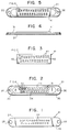
- Figs. 1 to 5 show the overlay laminate per se, as comprising three layers or laminae.
- Substrate 21 is shown in Fig. 1, and is formed of an electrical insulation film, such as Kapton or other flexible resin material.
- the electrically conductive elements of the overlay are preferably formed by etching a metallic conductive layer adhered to the substrate.
- the resultant conductive lamina 31 is shown in Fig. 2, applied to the substrate 21, and includes the conductive pads 32 and the encircling ground plane or ground strip 33.
- the ground strip 33 preferably surrounds the pattern of pads 32, and the pads are located so that an edge of each pad is adjacent to, but still slightly spaced from an edge of the ground strip, as shown at 34.
- the two ends of the ground strip are formed with projecting tabs 35, each having a hole 36. The tabs and holes are designed to facilitate grounding connection for the ground strip 33, as will be described subsequently.
- each pad 32 has a central opening 36, and is formed with opposed tabs 37 that project into the opening 36.
- the purpose of this pair of tabs is frictionally to engage a connector pin, when one is inserted in the opening 36, to make good electrical contact, as will be explained below.
- Fig. 6 also shows the spacing 34 between the opposed edges 38 and 39 of the tab 32 and ground strip 33.
- the etched conductor elements 32 and 33 on the substrate 21 are covered by thin insulative film 41, which may be Kapton or any other suitable flexible resin material.
- the cover 41 is shown in Fig. 3.
- the resulting laminate thus comprises three thin superposed layers 21, 31 and 41 as shown in Fig. 4.
- the cover lamina 41 has a series of openings 42 which correspond to the same series of openings 22 in the substrate, and when the three laminae are properly superposed as in Figs. 4 and 5, the openings 22 and 42 correspondingly align with the openings 36 in each of the pads 32. While the openings 22 and 42 in the substrate and cover are the same size, and are at least as large as the cross section of the connector pin to be received therein, as shown in Fig. 2 and the enlarged fragmentary views of Figs. 6 and 8, the tabs 37 of pads 32 project into the area of those openings.
- each opening 43 spans an edge portion 38 of the pad under the respective opening 42 and an adjacent edge portion 39 of the ground strip 33, along with the small spacing 34 between the pad and strip, as is best shown in the enlarged fragmentary view of Fig. 8.
- each of the openings 43 in the cover 41 is filled with an electrical overstress pulse protection composite 62 (see Fig. 12) of the general type aforedescribed.
- the composite is applied in a sufficiently fluid state as to enter the space 34 between edges 38 and 39 of pads 32 and ground strip 33. This may be done, for example, by painting or by silk screening the composite onto the cover 41 of the laminate through a screen pattern that corresponds to the assembled openings 43. This is illustrated in the cross section of Fig. 12, showing the completed laminate applied over the pins of a connector, as in Fig. 10.
- the laminate With the laminate now completed, it may be applied over an array of connector pins 51.
- the pin array must, of course, correspond to the pattern of openings and apertured pads in the laminate.
- the laminate is then driven or slid axially along the connector pins down to the base of the pins and resides as an overlay on the base of the connector 52, as shown in Fig. 10. In so doing, the tabs 37 on pads 32 are bent and resiliently engage the respective pins 51 to make good electrical contact therewith.
- the holes 36 in the ground strip tabs 35 are smaller than the holes 23 in the substrate tabs 24.
- the holes 36 and tabs 35 overlie the holes 23 and the tabs 24, and the ends of cover lamina 41 terminate short of the tabs.
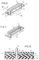
- FIG. 9 An alternative form of the invention is shown in Figs. 9 and 11.
- the basic structure of the flexible overlay 61 is the same as in the foregoing embodiment, except the ends or grounding tabs are different.
- the substrate, etched conductive lamina, and cover lamina are all essentially coextensive, except the ground plane or strip has resilient fingers 63 protruding from the ends of the laminate.
- the protruding clips 63 engage the inside of the connector shield, to effect a potential ground connection for the connector pins in the same way as the preceding embodiment.
- Example I Material Particle Size (less than) Vol. % 304 stainless steel 45 microns 22 Zinc oxide 5 microns 10 Silicon carbide 20 microns 10 Liquid Silicone (viscosity less than 500 cps) 58
- Example II Material Particle Size (less than) Vol.
- the ingredients are degassed and mixed to form a substantially homogenous composite, and the product is then applied by silk-screening or painting through the holes 43 in cover 41 into the gap 34 between edges 38 and 39.
- the gap 34 should be greater than 1.5 times the maximum conductor particle size, or twice the mean particle size, which ever is larger.
- the response of the composite material to electrical overstress pulses and the clamping voltage obtained is, of course, a function of the composition of the composite and the size of the gap 34, and for each application the laminate of the invention may be tailored accordingly.
- a flexible connector overlay which is applied over the pins of a prefabricated standard connector.
- the overlay is, of course, formed to accord with any desired connector design. Once applied to the connector, it provides protection to the circuits of which the connector is a part, against high voltage electrical overstress pulses by shunting the pulses to ground and clamping the pulse voltage at some voltage level that will not harm the circuit.
- This has been accomplished by the overlay laminate structure specifically shown and described in the foregoing specification and accompanying drawings.
- the present invention is not limited to the embodiments herein shown and described, and various modifications will be apparent to those skilled in the art, as well as adaptations to other circuit elements than connectors. Such modifications and adaptations as are embraced by the spirit and scope of the appended claims are contemplated as being within the purview of the present invention.
Abstract
A thin flexible laminate for overlay application on the pins (51) of a connector (52) or other circuit element comprises an electrically insulating substrate (21), a conductive lamina (31) of apertured pin-receiving pads (32), a separate ground strip (33) adjacent the pads (32), and an electrically insulating cover lamina (41). The substrate (21) and cover (41) have apertures (22 and 42) aligned with the pad apertures (36). The cover (41) has second apertures (43) exposing adjacent edges (38 and 39) of said pads (32) and ground strip (33). An electrical overstress pulse responsive composite material (62) is positioned in the second apertures (43) and bridges the pads (32) and the ground strip (33).
Description
- The present invention relates to the protection of electrical and electronic circuits from high energy electrical overstress pulses that might be injurious or destructive to the circuits, and render them non-functional, either permanently or temporarily. Suitable non-linear compositions and composite formulations of materials are known which can be connected to, or incorporated as part of an electrical circuit, and are characterized by high electrical resistance when exposed to low or normal operating voltages, but essentially instantaneously switch to low electrical resistance in response to an excessive or overstress voltage pulse, thereby shunting the excessive voltage or overstress pulse to ground. The present invention relates particularly to structural arrangements for the inclusion of those non-linear materials into electrical circuits, and more specifically into electrical connectors.
- The materials utilized in practicing the present invention are designed to respond substantially instantaneously to the leading edge of an overstress voltage pulse by changing their electrical characteristics, and by shunting the pulse to ground, to reduce the transmitted voltage of the pulse to a much lower value, and to clamp the voltage at that lower value for the duration of the pulse. These materials are also capable of substantially instantaneous recovery to their original high resistance value on termination of the overstress pulse, and of repeated responses to repetitive overstress pulses. For example, these materials can be designed to provide an ohmic resistance in the megohm range in the presence of low applied voltages in the range of 10 to more than 100 volts. However, upon the application of a sudden overstress pulse of, for example, 4,000 volts, these materials essentially instantaneously drop in resistance and switch to a low impedance shunt state that reduces the overstress pulse to a value in the range of a few hundred volts, or less, and clamps the voltage at that low value for the duration of the pulse. In the present description, the high resistance state is called the "off-state", and the low resistance condition under overstress is called the "on-state".
- Overstress responsive compositions are known in the art, and in general, they constitute a mixture or composite of finely divided electrically conductive and semiconductive particles supported in fixed spaced relation to each other in an electrically insulative resin binder or matrix. The most effective of these compositions or composites is described in U.S. Patent No. 4,992,333. The entire teaching of said application is incorporated herein by reference. In general, said composite comprises a mixture of different micron sized particles of conductive and semiconductive materials with angstrom sized spacer particles, which are densely packed and bound with an insulative resin matrix. Other electrical overstress compositions are described and illustrated in other prior art patents.
- U.S. Patent 2,273,704 to R.O. Grisdale discloses a granular composite material having a non-linear voltage-current characteristic. This patent discloses a mixture of conductive and semiconductive granules that are coated with a thin insulative film (such as metal oxides), and are compressed and bonded together in a matrix to provide stable, intimate and permanent contact between the granules.
- U.S. patent 4,097,834 to K.M. Mar et al. provides an electronic circuit protective device in the form of a thin film non-linear resistor, comprising conductive particles surrounded by a dielectric material, and coated onto a semiconductor substrate.
- U.S patent 2,796,505 to C.V. Bocciarelli discloses a non-linear precision voltage regulating element comprised of conductor particles having insulative oxide coatings thereon that are bound in a matrix. The particles are irregular in shape, and are point contiguous, i.e. the particles make point contact with each other.
- U.S. patent 4,726,991 to Hyatt et al. discloses an electrical overstress protection material, comprised of a mixture of conductive and semiconductive particles, all of whose surfaces are located with an insulative oxide film, and which are bound together in an insulative matrix, wherein the coated particles are in contact, preferably point contact, with each other.
- Additional patents illustrative of the prior art in respect to this general type of non-linear resistor are U.S. patent 2,150,167 to Hutchins et al., 2,206,792 to Stalhana, 3,864,658 to Pitha et al., and 4,977,357 and 5,068,634 to Shrier.
- As illustrated in the foregoing prior art, the overstress responsive compositions are usually positioned as a bulk material between a pair of contraposed electrodes having large areas facing each other, and the compositions are confined or clamped between the electrode structures. Because the matrix binder usually and preferably is a resin, the compression force applied during assembly of the electrodes and the composition affects the electrical properties of the resultant unit, and in use, changes in compression due to structural expansion and contraction likewise affects the electrical properties. Thus, both the off-state resistance and on-state resistance of these devices can vary, as well as the value of the overstress voltage at which the devices will switch from off-state to on-state and the voltage at which the overstress pulse is clamped for its duration.
- The copending patent application of Roger C. Stephenson and Hugh H. Hyatt, S.N. 666,026, filed March 7, 1991 provides a structure wherein the aforesaid difficulties are mitigated and effectively eliminated, and in addition, certain performance improvements are obtained. That application utilizes an edge electrode for at least one of the electrodes, and in certain embodiments both may be edge electrodes. To this end, said at least one electrode is formed from or with a thin metal lamina, and the thin edge of the lamina is used as the face of the electrode. This thin edge is placed in spaced contraposed relation to the face of the second electrode, and the latter face may itself be a thin edge, or it may be a relatively large flat surface area, or it may be the curved face of a cylindrical electrode such as a connector pin. The non-linear resistance composite material is interposed between the two electrode faces and makes electrical contact therewith In the preferred arrangement, the thickness of the thin edge electrode(s) is less than the spacing between the electrodes. Because of this geometry, the interposed composite materials is not subjected to the compressive action of contraposed large area electrode surfaces. In addition, the edge effect of the electrode enhances the local electric field and causes the composite material to switch from its off-state to its on-state earlier in the presence of an overstress electrical pulse, than with a comparable device where the contraposed faces of the electrodes present large areas. Also, when in the off-state, the resistance of the interposed composite is greater than with a comparable structure where the contraposed faces of the electrodes present large areas.
- The thin lamina electrode may be a printed circuit element or ground plane, which would place its thickness at about 0.2 to 35 mils; or it may be a self-sustaining metal foil, which would place its thickness in the range of about 1 to 50 mils; or it may be a thin metal sheet of 50 mils or greater, preferably, but not limited to, up to about a tenth of an inch.
- The present invention is an improvement over the teachings of said Stephenson and Hyatt application, and is an adaptation of the teachings thereof, useful particularly for application to electrical connectors. In accordance with the present invention a very thin, and preferably flexible laminate is formed, comprising an insulative substrate lamina carrying a printed or etched conductive lamina on one surface with a second insulative covering lamina placed over the conductive lamina. The conductive lamina includes two types of conductive elements; the first type is a connector pin-engaging pad, and the second type is a ground plane or strip. Normally, there is a separate apertured pad for each pin, which is designed to slide over the respective pin axially, and frictionally to engage and make electrical contact with the pin. The ground plane is electrically separate from the pads but is configured to have an edge located closely adjacent an edge of each pad. The space between each pad and the ground plane is bridged with an appropriate overstress composite material, such as aforedescribed. Thus, if an overstress electrical pulse appears at one or more of the connector pins, it turns the composite to its on-state and is thus shunted to ground via the ground plane.
- The aforesaid laminate is preferably formed of flexible laminae, and is shaped to conform to the connector housing, with the pads arranged to conform to the pin configuration. The insulative substrate and cover laminae are provided with holes or apertures that also conform with the pad apertures and connector pin configuration. Thus, the laminate is readily applied as an overlay to a completely fabricated connector for which it is designed, by being positioned over the pins of the connector, and then slid axially along the pins to their base. One or more terminals are provided on the ground plane for making electrical contact with a ground connection, which may be one of the connector pins or the connector housing. Although the laminate is contemplated as best adapted for application to a connector, the principle of the invention is applicable to other circuit structures.
- Accordingly, it is one object of the present invention to provide a laminate or overlay adapted to be applied to an electrical circuit element for inclusion of an electrical overstress pulse responsive composite material in the electrical circuit of the element.
- Another object of the present invention is to provide such a laminate adapted to be applied over the pins of an electrical circuit connector for inclusion of an electrical overstress pulse responsive composite material in the circuit of the connector.
- Still another object of the present invention is to provide a planar overlay adapted to be applied to a circuit element, such as over the pins of an electrical connector, for inclusion of an electrical overstress pulse responsive composite material in the electrical circuit.
- And a further object of the invention is to provide such an overlay formed as a flexible laminate of a pattern of electrically conductive elements and an electrically insulating carrier therefor, with an electrical overstress pulse responsive composite material interposed between portions of said conductive elements.
- Other objects and advantages of the present invention will become apparent to those skilled in the art from a consideration of the illustrative specific embodiments of the invention provided in the following detailed description, had in conjunction with the accompanying drawings, in which like reference characters refer to like or corresponding parts.
-
- Fig. 1 is plan view of a substrate lamina used in the present invention;
- Fig. 2 is a plan view of the substrate lamina with a conductive lamina applied thereto;
- Fig. 3 is a plan view of a cover lamina to be applied over the conductive lamina shown in Fig. 2;
- Fig. 4 is an edge view of the assembled laminae of Figs. 1, 2 and 3;
- Fig. 5 is a plan view of the assembled laminae of Figs. 1, 2 and 3;
- Fig. 6 is an enlarged view of a portion of Fig. 2;
- Fig. 7 is an enlarged view of a portion of Fig. 3;
- Fig. 8 is an enlarged view of a portion of Fig. 5;
- Fig. 9 is a perspective view of a modified form of the invention;
- Fig. 10 is a perspective view of a connector with the embodiment of the invention as shown in Fig. 1-5 applied thereto;
- Fig. 11 is a perspective view of a connector with the embodiment of the invention as shown in Fig. 9 applied thereto; and
- Fig. 12 is a cross sectional view of Fig. 10 taken along the line 12-12.
- Referring to the drawings, Figs. 1 to 5 show the overlay laminate per se, as comprising three layers or laminae.
Substrate 21 is shown in Fig. 1, and is formed of an electrical insulation film, such as Kapton or other flexible resin material. The electrically conductive elements of the overlay are preferably formed by etching a metallic conductive layer adhered to the substrate. The resultantconductive lamina 31 is shown in Fig. 2, applied to thesubstrate 21, and includes theconductive pads 32 and the encircling ground plane orground strip 33. Theground strip 33 preferably surrounds the pattern ofpads 32, and the pads are located so that an edge of each pad is adjacent to, but still slightly spaced from an edge of the ground strip, as shown at 34. In the form shown in Fig. 2, the two ends of the ground strip are formed with projectingtabs 35, each having ahole 36. The tabs and holes are designed to facilitate grounding connection for theground strip 33, as will be described subsequently. - The form of the
pads 32 is shown in the enlarged fragmentary view of Fig 6. Each pad has acentral opening 36, and is formed withopposed tabs 37 that project into theopening 36. The purpose of this pair of tabs is frictionally to engage a connector pin, when one is inserted in theopening 36, to make good electrical contact, as will be explained below. Fig. 6 also shows the spacing 34 between theopposed edges tab 32 andground strip 33. - The etched
conductor elements substrate 21 are covered bythin insulative film 41, which may be Kapton or any other suitable flexible resin material. Thecover 41 is shown in Fig. 3. - The resulting laminate thus comprises three thin
superposed layers cover lamina 41 has a series ofopenings 42 which correspond to the same series ofopenings 22 in the substrate, and when the three laminae are properly superposed as in Figs. 4 and 5, theopenings openings 36 in each of thepads 32. While theopenings tabs 37 ofpads 32 project into the area of those openings. - In addition to the
pin receiving openings 42 in thecover lamina 41, there is an additionalsmall opening 43 associated with and adjacent to eachopening 42. Eachopening 43 spans anedge portion 38 of the pad under therespective opening 42 and anadjacent edge portion 39 of theground strip 33, along with thesmall spacing 34 between the pad and strip, as is best shown in the enlarged fragmentary view of Fig. 8. - After this laminate has been assembled and the laminae are adhered together, each of the
openings 43 in thecover 41 is filled with an electrical overstress pulse protection composite 62 (see Fig. 12) of the general type aforedescribed. The composite is applied in a sufficiently fluid state as to enter thespace 34 betweenedges pads 32 andground strip 33. This may be done, for example, by painting or by silk screening the composite onto thecover 41 of the laminate through a screen pattern that corresponds to the assembledopenings 43. This is illustrated in the cross section of Fig. 12, showing the completed laminate applied over the pins of a connector, as in Fig. 10. - With the laminate now completed, it may be applied over an array of connector pins 51. The pin array must, of course, correspond to the pattern of openings and apertured pads in the laminate. The laminate is then driven or slid axially along the connector pins down to the base of the pins and resides as an overlay on the base of the
connector 52, as shown in Fig. 10. In so doing, thetabs 37 onpads 32 are bent and resiliently engage therespective pins 51 to make good electrical contact therewith. - It will be observed that the
holes 36 in theground strip tabs 35 are smaller than theholes 23 in thesubstrate tabs 24. Theholes 36 andtabs 35 overlie theholes 23 and thetabs 24, and the ends ofcover lamina 41 terminate short of the tabs. Thus, when assembled to a connector of corresponding configuration as shown in Fig. 10, theconductive tabs 35 are firmly engaged or grounded to the connector housing by threadedbolts 53 which pass throughholes conductive tabs 35. There is thus provided the potential for a conductive path from any of the connector pins 51 to itsrespective pad 32, across the electrical overstress responsive composite 62bridging gap 34, to groundstrip 33, and thence throughtab 35 to ground. - An alternative form of the invention is shown in Figs. 9 and 11. The basic structure of the
flexible overlay 61 is the same as in the foregoing embodiment, except the ends or grounding tabs are different. In the embodiment of Fig. 9, the substrate, etched conductive lamina, and cover lamina are all essentially coextensive, except the ground plane or strip hasresilient fingers 63 protruding from the ends of the laminate. Thus, when this laminate is applied over the pins of a shielded pin connector, such as in Fig. 11, and is slid over the pins to the base of the connector, the protruding clips 63 engage the inside of the connector shield, to effect a potential ground connection for the connector pins in the same way as the preceding embodiment. - As the electrical overstress pulse responsive composite material, the following compositions are most useful for filing the
small gaps 34 and the small holes 43.Example I Material Particle Size (less than) Vol. % 304 stainless steel 45 microns 22 Zinc oxide 5 microns 10 Silicon carbide 20 microns 10 Liquid Silicone (viscosity less than 500 cps) 58 Example II Material Particle Size (less than) Vol. % 304 stainless steel 45 microns 22 Zinc oxide 5 microns 10 Silicon carbide 20 microns 10 Epoxy resin plus catalyst (viscosity about 7000 cps) 58
In both examples, the ingredients are degassed and mixed to form a substantially homogenous composite, and the product is then applied by silk-screening or painting through theholes 43 incover 41 into thegap 34 betweenedges gap 34 should be greater than 1.5 times the maximum conductor particle size, or twice the mean particle size, which ever is larger. The response of the composite material to electrical overstress pulses and the clamping voltage obtained is, of course, a function of the composition of the composite and the size of thegap 34, and for each application the laminate of the invention may be tailored accordingly. - Thus, in accordance with the present invention there is provided a flexible connector overlay, which is applied over the pins of a prefabricated standard connector. The overlay is, of course, formed to accord with any desired connector design. Once applied to the connector, it provides protection to the circuits of which the connector is a part, against high voltage electrical overstress pulses by shunting the pulses to ground and clamping the pulse voltage at some voltage level that will not harm the circuit. This has been accomplished by the overlay laminate structure specifically shown and described in the foregoing specification and accompanying drawings. The present invention, however, is not limited to the embodiments herein shown and described, and various modifications will be apparent to those skilled in the art, as well as adaptations to other circuit elements than connectors. Such modifications and adaptations as are embraced by the spirit and scope of the appended claims are contemplated as being within the purview of the present invention.
Claims (15)
- An electrical overstress pulse arrester in the form of an overlay, comprising an electrically insulating substrate (21), an electrically conductive ground plane (33) on said substrate, a separate electrically conductive pad (32) on said substrate, and an electrically insulative cover (41) over said ground plane and pad, said pad (32) and said ground plane (33) having spaced adjacent edges (38 and 39), said pad having an aperture therein (36), said substrate having an aperture (22) underlying said pad aperture (36), said cover having a first aperture (42) overlying said pad aperture (36) and a second aperture (43) overlying said spaced adjacent edges (38 and 39), said ground plane (33) having ground connecting means (35), and an electrical overstress pulse responsive composite material (62) located in said second cover aperture (43) and interconnecting said pad (32) and said ground plane (33), said composite material (62) having the characteristics of a high electrical resistance in the presence of a low voltage applied across said material and a low electrical resistance in the presence of a high voltage applied across said material.
- An electrical overstress pulse arrester as set forth in Claim 1, said pad aperture (36), substrate aperture and first cover aperture (42) being adapted to receive a conductive circuit element (51) therethrough, and said pad having electrical contact means (37) for engaging said conductive circuit element (51).
- An electrical overstress pulse arrester as set forth in Claims 1 or 2, having a plurality of said pads (32), each pad having an aperture (36) and an edge (38) spaced from and adjacent an edge (39) of said ground plane (33), said substrate having a plurality of apertures (22) underlying the pad apertures (36), said cover having a plurality of said first apertures overlying the pad apertures and a plurality of said second apertures (43) overlying the plurality of said spaced adjacent edges (38 and 39), and said composite material (62) located in said plurality of second cover apertures (43).
- An electrical overstress pulse arrester for pin connectors in the form of an overlay, comprising an electrically insulating substrate (21), an electrically conductive lamina (31) on said substrate comprising a ground plane (33) and a separate pad (32), and an electrically insulative cover (41) over said lamina, said ground plane (33) and said pad (32) having spaced adjacent edges (38 and 39), said pad having an aperture (36) for receiving therethrough the pin (51) of a connector (52), said pad (32) having means (37) for electrically engaging said pin when received therethrough, said substrate (21) and said cover (41) each having an aperture (22, 42) located in correspondence with the aperture (36) in said pad for receiving said pin (51) therethrough, one of said substrate and cover having a second aperture (43) coincident with said spaced edges (38 and 39), said ground plane (33) having ground connecting means (35), and an electrical overstress pulse responsibe composite material (62) located in said second aperture (43) interconnecting said spaced edges (38 and 39), said composite material having the characteristics of a high electrical resistance in the presence of a low voltage applied across said material and a low electrical resistance in the presence of a high voltage applied across said material.
- An electrical overstress pulse arrester as set forth in Claim 4, having a plurality of apertured pads (32), said substrate (21) and cover (41) each having a plurality of apertures (22, 42) located in correspondence with said plurality of apertured pads (32) for receiving a plurality of connector pins (51) therethrough, and a plurality of said second apertures (43).
- In combination, a connector (52) having a plurality of pins (51) and a laminate overlayed on said pins, said laminate overlay comprising an electrically insulating substrate (21), an electrically conductive lamina (31) on said substrate comprising a ground plane (33) and a plurality of separate pads (32), and an electrically insulating cover (41) over said lamina, said pads (32) each having an edge (38) adjacent an edge (39) of said ground plane and spaced therefrom, each pad having an aperture (36) and the substrate and cover each having a set of apertures (22 and 42) in correspondence with the pad apertures (36) receiving said pins (51), one of said substrate and said cover having a second set of apertures (43) coincident with said spaced edges (38 and 39) for each pad, and an electrical overstress pulse responsive composite material (62) located in said second set of apertures (43) interconnecting said spaced edges, said composite material having the characteristics of a high electrical resistance in the presence of a low voltage applied across said material and a low electrical resistance in the presence of a high voltage applied across said material.
- In the combination as set forth in Claim 6, means (53, 63) coupling said ground plane (33) to a ground element on said connector (52).
- In the combination as set forth in Claims 6 or 7, each of said pads (32) having means (37) for electrically engaging the respective pin (51) received in the respective aperture (36).
- A laminate for forming an electrical overstress pulse arrester by overlay on a circuit element, comprising an electrically insulating substrate (21), an electrically conductive ground plane (33) and a separate electrically conductive pad (32) on said substrate, said ground plane (33) and said pad (32) having spaced adjacent edges (38 and 39), said pad and said substrate having superposed apertures (36, 22) therein for receiving a portion (51) of said circuit element, and electrical overstress pulse responsive composite material (62) located between and connecting said spaced adjacent edges (38 and 39), said composite material (62) having the characteristics of a high electrical resistance in the presence of a low voltage applied across said material and a low electrical resistance in the presence of a high voltage applied across said material.
- A laminate as set form in Claim 9, and further including an electrically insulating cover (41) over said ground plane (33).
- A laminate as set forth in Claims 9 or 10, and further including ground connecting means (35) for said ground plane (33) and circuit element connecting means (37) for said pad.
- A laminate for forming an electrical overstress pulse arrester by overlay on a circuit element, comprising an electrical insulating carrier (21), an electrically conductive ground plane (33) laminated to said carrier (21), an electrically conductive pad (32) laminated to said carrier in spaced adjacent relation to said ground plane (33), and an electrical overstress pulse responsive composite material (62) located between said ground plane (33) and pad (32) and connecting an edge of one to the other, said pad and carrier having aligned apertures (36, 22) for receiving a portion (51) of said circuit element therein, said pad having means (37) for making electrical contact with said portion of said circuit element, said ground plane having means (35) for making a ground connection.
- A laminate as set forth in Claim 12, and including a plurality of said pads, the carrier having a set of apertures corresponding to the apertures of the plurality of pads, said composite material being located between said ground plane and each of said pads and connecting an edge of one to the other.
- A laminate as set forth in Claim 13, in combination with a multipin connector (52), the pins (51) of said connector passing through said apertures (36, 22) of said pad (32) and said carrier (21).
- Apparatus according to any of the preceding claims, in which the laminate or overlay is thin and flexible.
Priority Applications (3)
| Application Number | Priority Date | Filing Date | Title |
|---|---|---|---|
| US07/928,034 US5278535A (en) | 1992-08-11 | 1992-08-11 | Electrical overstress pulse protection |
| AU48648/93A AU4864893A (en) | 1992-08-11 | 1993-09-28 | Electrical overstress pulse protection |
| EP93307784A EP0647952A1 (en) | 1992-08-11 | 1993-09-30 | Electrical overstress pulse protection |
Applications Claiming Priority (3)
| Application Number | Priority Date | Filing Date | Title |
|---|---|---|---|
| US07/928,034 US5278535A (en) | 1992-08-11 | 1992-08-11 | Electrical overstress pulse protection |
| AU48648/93A AU4864893A (en) | 1992-08-11 | 1993-09-28 | Electrical overstress pulse protection |
| EP93307784A EP0647952A1 (en) | 1992-08-11 | 1993-09-30 | Electrical overstress pulse protection |
Publications (1)
| Publication Number | Publication Date |
|---|---|
| EP0647952A1 true EP0647952A1 (en) | 1995-04-12 |
Family
ID=27154566
Family Applications (1)
| Application Number | Title | Priority Date | Filing Date |
|---|---|---|---|
| EP93307784A Withdrawn EP0647952A1 (en) | 1992-08-11 | 1993-09-30 | Electrical overstress pulse protection |
Country Status (3)
| Country | Link |
|---|---|
| US (1) | US5278535A (en) |
| EP (1) | EP0647952A1 (en) |
| AU (1) | AU4864893A (en) |
Families Citing this family (69)
| Publication number | Priority date | Publication date | Assignee | Title |
|---|---|---|---|---|
| US5973588A (en) * | 1990-06-26 | 1999-10-26 | Ecco Limited | Multilayer varistor with pin receiving apertures |
| DE69314742T2 (en) * | 1992-09-23 | 1998-02-19 | Whitaker Corp | Protection against electrical overload |
| JP2591294Y2 (en) * | 1992-11-27 | 1999-03-03 | 北陸電気工業株式会社 | High voltage resistance pack |
| US5384435A (en) * | 1994-01-28 | 1995-01-24 | Molex Incorporated | Mounting terminal pins in substrates |
| US6191928B1 (en) | 1994-05-27 | 2001-02-20 | Littelfuse, Inc. | Surface-mountable device for protection against electrostatic damage to electronic components |
| KR100369681B1 (en) | 1994-07-14 | 2003-04-11 | 서직스 코퍼레이션 | Variable voltage protection structures and method for making same |
| ATE227881T1 (en) * | 1994-07-14 | 2002-11-15 | Surgx Corp | METHOD FOR PRODUCING SINGLE AND MULTI-LAYER PROTECTIVE DEVICES AGAINST VARIABLE VOLTAGE |
| WO1996005639A1 (en) * | 1994-08-08 | 1996-02-22 | Raychem Corporation | Protected telecommunications terminal |
| US6232866B1 (en) * | 1995-09-20 | 2001-05-15 | The United States Of America As Represented By The Administrator Of The National Aeronautics And Space Administration | Composite material switches |
| DE19643670A1 (en) * | 1995-10-31 | 1997-05-07 | Whitaker Corp | Over-voltage protection material curing at low temperature to avoid damage |
| JP3313271B2 (en) * | 1995-12-28 | 2002-08-12 | ウエスト電気株式会社 | Strobe device |
| US6172590B1 (en) * | 1996-01-22 | 2001-01-09 | Surgx Corporation | Over-voltage protection device and method for making same |
| EP0836249B1 (en) * | 1996-10-12 | 2002-03-27 | Molex Incorporated | Electrical grounding shroud |
| US6013358A (en) * | 1997-11-18 | 2000-01-11 | Cooper Industries, Inc. | Transient voltage protection device with ceramic substrate |
| TW353183B (en) * | 1996-12-27 | 1999-02-21 | Hokuriku Elect Ind | Electric component and variable resistor for high voltage use |
| US5897388A (en) * | 1997-05-30 | 1999-04-27 | The Whitaker Corporation | Method of applying ESD protection to a shielded electrical |
| US6251513B1 (en) | 1997-11-08 | 2001-06-26 | Littlefuse, Inc. | Polymer composites for overvoltage protection |
| EP0921596A1 (en) * | 1997-11-24 | 1999-06-09 | Molex Incorporated | Terminal blades mounted on flexible substrates |
| US6642297B1 (en) | 1998-01-16 | 2003-11-04 | Littelfuse, Inc. | Polymer composite materials for electrostatic discharge protection |
| US6064094A (en) * | 1998-03-10 | 2000-05-16 | Oryx Technology Corporation | Over-voltage protection system for integrated circuits using the bonding pads and passivation layer |
| US6549114B2 (en) * | 1998-08-20 | 2003-04-15 | Littelfuse, Inc. | Protection of electrical devices with voltage variable materials |
| USD425481S (en) * | 1999-06-24 | 2000-05-23 | James Cutler | Lightning discharge strip |
| US7446030B2 (en) * | 1999-08-27 | 2008-11-04 | Shocking Technologies, Inc. | Methods for fabricating current-carrying structures using voltage switchable dielectric materials |
| US20100044079A1 (en) * | 1999-08-27 | 2010-02-25 | Lex Kosowsky | Metal Deposition |
| US20100044080A1 (en) * | 1999-08-27 | 2010-02-25 | Lex Kosowsky | Metal Deposition |
| WO2001017320A1 (en) | 1999-08-27 | 2001-03-08 | Lex Kosowsky | Current carrying structure using voltage switchable dielectric material |
| US7695644B2 (en) | 1999-08-27 | 2010-04-13 | Shocking Technologies, Inc. | Device applications for voltage switchable dielectric material having high aspect ratio particles |
| US20080035370A1 (en) * | 1999-08-27 | 2008-02-14 | Lex Kosowsky | Device applications for voltage switchable dielectric material having conductive or semi-conductive organic material |
| US7825491B2 (en) * | 2005-11-22 | 2010-11-02 | Shocking Technologies, Inc. | Light-emitting device using voltage switchable dielectric material |
| US6628498B2 (en) | 2000-08-28 | 2003-09-30 | Steven J. Whitney | Integrated electrostatic discharge and overcurrent device |
| JP4237615B2 (en) * | 2001-07-10 | 2009-03-11 | リッテルフューズ,インコーポレイティド | Electrostatic discharge device for network devices |
| US6547597B2 (en) | 2001-07-10 | 2003-04-15 | Littelfuse, Inc. | Apparatus and method for incorporating surface mount components into connectors |
| US6935879B2 (en) * | 2001-07-10 | 2005-08-30 | Littelfuse, Inc. | Connectors having circuit protection |
| US7034652B2 (en) * | 2001-07-10 | 2006-04-25 | Littlefuse, Inc. | Electrostatic discharge multifunction resistor |
| US7258819B2 (en) | 2001-10-11 | 2007-08-21 | Littelfuse, Inc. | Voltage variable substrate material |
| US6809625B2 (en) * | 2001-12-20 | 2004-10-26 | Intel Corporation | Integrated connector and positive thermal coefficient switch |
| US7183891B2 (en) * | 2002-04-08 | 2007-02-27 | Littelfuse, Inc. | Direct application voltage variable material, devices employing same and methods of manufacturing such devices |
| US7132922B2 (en) * | 2002-04-08 | 2006-11-07 | Littelfuse, Inc. | Direct application voltage variable material, components thereof and devices employing same |
| CN100350606C (en) * | 2002-04-08 | 2007-11-21 | 力特保险丝有限公司 | Voltage variable material for direct application and devices employing same |
| US20060152334A1 (en) * | 2005-01-10 | 2006-07-13 | Nathaniel Maercklein | Electrostatic discharge protection for embedded components |
| WO2007062122A2 (en) | 2005-11-22 | 2007-05-31 | Shocking Technologies, Inc. | Semiconductor devices including voltage switchable materials for over-voltage protection |
| US20100263200A1 (en) * | 2005-11-22 | 2010-10-21 | Lex Kosowsky | Wireless communication device using voltage switchable dielectric material |
| US8030575B2 (en) * | 2005-12-29 | 2011-10-04 | Sensor Electronic Technology, Inc. | Mounting structure providing electrical surge protection |
| US7571628B2 (en) * | 2006-06-22 | 2009-08-11 | D Anieri Marissa S | Electronic locking system for vehicles |
| US20080032049A1 (en) * | 2006-07-29 | 2008-02-07 | Lex Kosowsky | Voltage switchable dielectric material having high aspect ratio particles |
| US20080029405A1 (en) * | 2006-07-29 | 2008-02-07 | Lex Kosowsky | Voltage switchable dielectric material having conductive or semi-conductive organic material |
| US7968010B2 (en) * | 2006-07-29 | 2011-06-28 | Shocking Technologies, Inc. | Method for electroplating a substrate |
| EP2084748A4 (en) | 2006-09-24 | 2011-09-28 | Shocking Technologies Inc | Formulations for voltage switchable dielectric material having a stepped voltage response and methods for making the same |
| FR2908240B1 (en) * | 2006-11-06 | 2009-01-30 | Souriau Soc Par Actions Simpli | ELECTRICAL CONNECTOR FILTER EQUIPPED WITH CONTACTS PROTECTED INDIVIDUALLY AGAINST TRANSIENTS |
| US7309246B1 (en) * | 2006-11-20 | 2007-12-18 | Tyco Electronics Corporation | Electrical connector with ESD protection |
| US20120119168A9 (en) * | 2006-11-21 | 2012-05-17 | Robert Fleming | Voltage switchable dielectric materials with low band gap polymer binder or composite |
| US7793236B2 (en) * | 2007-06-13 | 2010-09-07 | Shocking Technologies, Inc. | System and method for including protective voltage switchable dielectric material in the design or simulation of substrate devices |
| US8206614B2 (en) * | 2008-01-18 | 2012-06-26 | Shocking Technologies, Inc. | Voltage switchable dielectric material having bonded particle constituents |
| US7952848B2 (en) | 2008-04-04 | 2011-05-31 | Littelfuse, Inc. | Incorporating electrostatic protection into miniature connectors |
| US8203421B2 (en) * | 2008-04-14 | 2012-06-19 | Shocking Technologies, Inc. | Substrate device or package using embedded layer of voltage switchable dielectric material in a vertical switching configuration |
| US20100047535A1 (en) * | 2008-08-22 | 2010-02-25 | Lex Kosowsky | Core layer structure having voltage switchable dielectric material |
| WO2010033635A1 (en) * | 2008-09-17 | 2010-03-25 | Shocking Technologies, Inc. | Voltage switchable dielectric material containing boron compound |
| US9208931B2 (en) * | 2008-09-30 | 2015-12-08 | Littelfuse, Inc. | Voltage switchable dielectric material containing conductor-on-conductor core shelled particles |
| US9208930B2 (en) * | 2008-09-30 | 2015-12-08 | Littelfuse, Inc. | Voltage switchable dielectric material containing conductive core shelled particles |
| US8362871B2 (en) * | 2008-11-05 | 2013-01-29 | Shocking Technologies, Inc. | Geometric and electric field considerations for including transient protective material in substrate devices |
| US9226391B2 (en) | 2009-01-27 | 2015-12-29 | Littelfuse, Inc. | Substrates having voltage switchable dielectric materials |
| US8272123B2 (en) | 2009-01-27 | 2012-09-25 | Shocking Technologies, Inc. | Substrates having voltage switchable dielectric materials |
| US8399773B2 (en) | 2009-01-27 | 2013-03-19 | Shocking Technologies, Inc. | Substrates having voltage switchable dielectric materials |
| EP2412212A1 (en) | 2009-03-26 | 2012-02-01 | Shocking Technologies Inc | Components having voltage switchable dielectric materials |
| US9053844B2 (en) * | 2009-09-09 | 2015-06-09 | Littelfuse, Inc. | Geometric configuration or alignment of protective material in a gap structure for electrical devices |
| US20110198544A1 (en) * | 2010-02-18 | 2011-08-18 | Lex Kosowsky | EMI Voltage Switchable Dielectric Materials Having Nanophase Materials |
| US9320135B2 (en) * | 2010-02-26 | 2016-04-19 | Littelfuse, Inc. | Electric discharge protection for surface mounted and embedded components |
| US9224728B2 (en) * | 2010-02-26 | 2015-12-29 | Littelfuse, Inc. | Embedded protection against spurious electrical events |
| US9082622B2 (en) | 2010-02-26 | 2015-07-14 | Littelfuse, Inc. | Circuit elements comprising ferroic materials |
Citations (5)
| Publication number | Priority date | Publication date | Assignee | Title |
|---|---|---|---|---|
| US4097834A (en) * | 1976-04-12 | 1978-06-27 | Motorola, Inc. | Non-linear resistors |
| EP0211508A1 (en) * | 1985-07-26 | 1987-02-25 | Amp Incorporated | Transient suppression device |
| US4726991A (en) * | 1986-07-10 | 1988-02-23 | Eos Technologies Inc. | Electrical overstress protection material and process |
| US5183698A (en) * | 1991-03-07 | 1993-02-02 | G & H Technology, Inc. | Electrical overstress pulse protection |
| US5246388A (en) * | 1992-06-30 | 1993-09-21 | Amp Incorporated | Electrical over stress device and connector |
Family Cites Families (2)
| Publication number | Priority date | Publication date | Assignee | Title |
|---|---|---|---|---|
| US3740701A (en) * | 1971-12-22 | 1973-06-19 | Gen Electric | Protective connector devices |
| US5006950A (en) * | 1986-10-28 | 1991-04-09 | Allina Edward F | Electrical transient surge protection with parallel means |
-
1992
- 1992-08-11 US US07/928,034 patent/US5278535A/en not_active Expired - Lifetime
-
1993
- 1993-09-28 AU AU48648/93A patent/AU4864893A/en not_active Abandoned
- 1993-09-30 EP EP93307784A patent/EP0647952A1/en not_active Withdrawn
Patent Citations (5)
| Publication number | Priority date | Publication date | Assignee | Title |
|---|---|---|---|---|
| US4097834A (en) * | 1976-04-12 | 1978-06-27 | Motorola, Inc. | Non-linear resistors |
| EP0211508A1 (en) * | 1985-07-26 | 1987-02-25 | Amp Incorporated | Transient suppression device |
| US4726991A (en) * | 1986-07-10 | 1988-02-23 | Eos Technologies Inc. | Electrical overstress protection material and process |
| US5183698A (en) * | 1991-03-07 | 1993-02-02 | G & H Technology, Inc. | Electrical overstress pulse protection |
| US5246388A (en) * | 1992-06-30 | 1993-09-21 | Amp Incorporated | Electrical over stress device and connector |
Also Published As
| Publication number | Publication date |
|---|---|
| AU4864893A (en) | 1995-05-04 |
| US5278535A (en) | 1994-01-11 |
Similar Documents
| Publication | Publication Date | Title |
|---|---|---|
| US5278535A (en) | Electrical overstress pulse protection | |
| US5183698A (en) | Electrical overstress pulse protection | |
| US5340641A (en) | Electrical overstress pulse protection | |
| US6693508B2 (en) | Protection of electrical devices with voltage variable materials | |
| US6211554B1 (en) | Protection of an integrated circuit with voltage variable materials | |
| AU704862B2 (en) | Variable voltage protection structures and methods for making same | |
| US5483407A (en) | Electrical overstress protection apparatus and method | |
| HK1006888A1 (en) | Self-regulating ptc devices having shaped laminar conductive terminals | |
| EP0357612A1 (en) | Electrical switching and control apparatus. | |
| EP1347470A1 (en) | Electrical devices comprising a conductive polymer | |
| US7035072B2 (en) | Electrostatic discharge apparatus for network devices | |
| DE19737261A1 (en) | Lead frame for encapsulated integrated circuit | |
| US6178078B1 (en) | Discharge gap device and its mounting structure | |
| JPH07114953A (en) | Avoidance device of electric excessive stress pulse | |
| DE69635078D1 (en) | ELECTRICAL DEVICE WITH PTC BEHAVIOR | |
| US20050024800A1 (en) | Voltage protection device | |
| CA1200585A (en) | High capacitance laminated bus | |
| US5576922A (en) | Surge absorbing structure, surge absorbing element, connector and circuit device using these structure and element | |
| KR100246730B1 (en) | Chip barristor and its setting apparatus | |
| JPS5852866A (en) | Integrated circuit | |
| JP2636213B2 (en) | Static electricity absorber | |
| JP2507907Y2 (en) | Antistatic circuit structure | |
| DE2848454C2 (en) | Arrangement for holding electrical systems against elements that protect against overvoltages | |
| JPS61232692A (en) | Printed wiring board | |
| JPS6338212A (en) | Surge noise absorber |
Legal Events
| Date | Code | Title | Description |
|---|---|---|---|
| PUAI | Public reference made under article 153(3) epc to a published international application that has entered the european phase |
Free format text: ORIGINAL CODE: 0009012 |
|
| AK | Designated contracting states |
Kind code of ref document: A1 Designated state(s): DE FR GB IT SE |
|
| STAA | Information on the status of an ep patent application or granted ep patent |
Free format text: STATUS: THE APPLICATION IS DEEMED TO BE WITHDRAWN |
|
| 18D | Application deemed to be withdrawn |
Effective date: 19951013 |