EP0652301A1 - Method for producing diamond-like coatings and coated articles made thereby - Google Patents
Method for producing diamond-like coatings and coated articles made thereby Download PDFInfo
- Publication number
- EP0652301A1 EP0652301A1 EP94115881A EP94115881A EP0652301A1 EP 0652301 A1 EP0652301 A1 EP 0652301A1 EP 94115881 A EP94115881 A EP 94115881A EP 94115881 A EP94115881 A EP 94115881A EP 0652301 A1 EP0652301 A1 EP 0652301A1
- Authority
- EP
- European Patent Office
- Prior art keywords
- carbon
- diamond
- coating
- cathode
- coatings
- Prior art date
- Legal status (The legal status is an assumption and is not a legal conclusion. Google has not performed a legal analysis and makes no representation as to the accuracy of the status listed.)
- Granted
Links
Images


Classifications
-
- C—CHEMISTRY; METALLURGY
- C23—COATING METALLIC MATERIAL; COATING MATERIAL WITH METALLIC MATERIAL; CHEMICAL SURFACE TREATMENT; DIFFUSION TREATMENT OF METALLIC MATERIAL; COATING BY VACUUM EVAPORATION, BY SPUTTERING, BY ION IMPLANTATION OR BY CHEMICAL VAPOUR DEPOSITION, IN GENERAL; INHIBITING CORROSION OF METALLIC MATERIAL OR INCRUSTATION IN GENERAL
- C23C—COATING METALLIC MATERIAL; COATING MATERIAL WITH METALLIC MATERIAL; SURFACE TREATMENT OF METALLIC MATERIAL BY DIFFUSION INTO THE SURFACE, BY CHEMICAL CONVERSION OR SUBSTITUTION; COATING BY VACUUM EVAPORATION, BY SPUTTERING, BY ION IMPLANTATION OR BY CHEMICAL VAPOUR DEPOSITION, IN GENERAL
- C23C14/00—Coating by vacuum evaporation, by sputtering or by ion implantation of the coating forming material
- C23C14/22—Coating by vacuum evaporation, by sputtering or by ion implantation of the coating forming material characterised by the process of coating
- C23C14/24—Vacuum evaporation
- C23C14/32—Vacuum evaporation by explosion; by evaporation and subsequent ionisation of the vapours, e.g. ion-plating
- C23C14/325—Electric arc evaporation
-
- C—CHEMISTRY; METALLURGY
- C23—COATING METALLIC MATERIAL; COATING MATERIAL WITH METALLIC MATERIAL; CHEMICAL SURFACE TREATMENT; DIFFUSION TREATMENT OF METALLIC MATERIAL; COATING BY VACUUM EVAPORATION, BY SPUTTERING, BY ION IMPLANTATION OR BY CHEMICAL VAPOUR DEPOSITION, IN GENERAL; INHIBITING CORROSION OF METALLIC MATERIAL OR INCRUSTATION IN GENERAL
- C23C—COATING METALLIC MATERIAL; COATING MATERIAL WITH METALLIC MATERIAL; SURFACE TREATMENT OF METALLIC MATERIAL BY DIFFUSION INTO THE SURFACE, BY CHEMICAL CONVERSION OR SUBSTITUTION; COATING BY VACUUM EVAPORATION, BY SPUTTERING, BY ION IMPLANTATION OR BY CHEMICAL VAPOUR DEPOSITION, IN GENERAL
- C23C14/00—Coating by vacuum evaporation, by sputtering or by ion implantation of the coating forming material
- C23C14/06—Coating by vacuum evaporation, by sputtering or by ion implantation of the coating forming material characterised by the coating material
- C23C14/0605—Carbon
Definitions
- the present invention relates to a method for producing diamond-like coatings and the coated articles made thereby.
- Amorphous carbon films having diamond-like properties of extreme hardness, extremely low electrical conductivity, low coefficients of friction, and optical transparency over a wide range of wavelengths have widespread applications as optical coatings, low friction, anti-corrosion coatings and wear-resistant coatings and in various other applications such as surface finishing and in semiconductor manufacturing.
- Diamond-like carbon is a non-crystalline, or amorphous, material having two types of carbon-carbon bonds, i.e., hexagonal graphite bonds (sp2) and tetrahedral diamond bonds (sp3). Thus, diamond-like carbon has both limited long range order and two types of short range order.
- Diamond-like carbon may be hydrogenated or non-hydrogenated.
- Hydrogenated diamond-like carbon is produced from a hydrocarbon gas mixture using various energy sources, e.g., DC discharge, microwave and RF energy, oxyacetylene torches, and hot filaments.
- Non-hydrogenated diamond-like coatings can be produced using magnetron sputtering, electron beam evaporation, laser ablation and mass filtered carbon-ion beam deposition techniques, each of which has a very low deposition rate.
- Each method for producing the non-hydrogenated diamond-like carbon produces a hard carbon coating but the coatings have differing sp3/sp2 bond ratios and, thus, the structural and physical characteristics differ.
- the sp3/sp2 bond ratio can be estimated from the plasmon energy determined by electron energy loss spectroscopy.
- the plasmon energy is proportional to the atom density and diamond has a greater atom density and plasmon energy than graphite.
- Polycrystalline graphite has a plasmon energy loss of about 25 electron volts (eV).
- Diamond has a plasmon energy loss of about 33 eV.
- Non-hydrogenated diamond-like carbon has a plasmon energy loss between about 26 and 32 eV, the higher plasmon energies corresponding to higher atom densities which are believed to be due to an increased sp3 bonding component.
- Hydrogen-free non-crystalline diamond-like carbon coatings can also be produced using cathodic arc plasma deposition, a process which provides high deposition rates and allows control over the incident ion kinetic energy and the substrate temperatures.
- the sp3/sp2 bond ratio is believed to be dependent on the incident ion kinetic energy.
- Cathodic arc plasma deposition can produce diamond-like carbon coatings with higher plasmon energies than alternative processes, thus, yielding higher sp3/sp2 bond ratios.
- a cathodic arc discharge occurs when a high current power source is connected between two sufficiently conductive electrodes and the electrodes are momentarily in contact, either physically or by another discharge.
- Arc spots form on the cathode surface as the electrodes are separated. These small, luminous regions are often very mobile and move rapidly over the cathode surface. Due to the high current density contained in each spot, rapid ebullition of the cathode material occurs, and this plasma material can be confined, transported using magnetic fields and deposited on substrates. The current density at each spot can reach 100,000 amperes per square centimeter and this contributes to the ionization of much of the outflowing vapor.
- Macroparticles are droplets or solid particles of the consumable cathode which range in size from about 0.1 micron to greater than about 50 microns, most being between about 0.5 and 20 microns. These macro particles are deposited with the plasma to produce unwanted particles in the final coating. Macroparticle production is particularly undesirable for diamond-like carbon coatings because they are graphite and become embedded in the diamond-like carbon coating. Much attention has been given to the removal of these particles.
- U.S. Pat. No. 4,452,686 (Axenov et al.) describes one means of macroparticle removal via filtration.
- a cylindrically shaped current coil and a central axially mounted, football-shaped coil produce a magnetic field that guides the plasma around the central coil and through the plasma guide system.
- Macroparticles, which are much heavier than the plasma particles are not guided by the magnetic field and, thus, are blocked by the central coil. Downstream, the plasma macroparticle density is significantly reduced.
- filtration means do reduce the macroparticle density in the coatings, they do not completely remove all macroparticles.
- the larger macroparticles are filtered, but the submicron particles are not completely filtered. This can occur as the submicron particles bounce around in the vacuum system. This can also result from momentum transfer from the plasma to the particles.
- plasma filters typically reduce the plasma flux by 30 to 50 percent, leading to reduced deposition rates.
- the present invention provides a method for producing a diamond-like carbon coating comprising the steps of providing a substrate to be coated, providing a cathode of vitreous carbon or pyrolytic graphite and initiating a cathodic arc discharge with the arc spot on the cathode surface and directing the resulting carbon plasma toward the substrate to form a coating on said substrate, said coating being substantially macroparticle free.
- the discharge may optionally be carried out in a magnetic field.
- the present invention overcomes the problem of macroparticles in diamond-like carbon coatings produced using a cathodic arc generator.
- the method of the presetn invention produces high quality, non-hydrogenated diamond-like coatings at high deposition rates.
- the present invention utilizes the cathodic arc process to produce non-hydrogenated, non-crystalline, diamond-like carbon coatings and films which are essentially macroparticle free. Unlike the prior art where the removal or filtration of the macroparticles was of prime concern, the present invention utilizes a cathodic arc carbon cathode material which does not generate macroparticles in the plasma discharge.
- the cathodic arc discharge coating process can be carried out under vacuum at pressues of, e.g., less than 10 ⁇ 3 Torr, at ambient conditions, e.g., room temperature of 20-25°C, in an inert atmosphere such as, for example, argon, or in a reactive atmosphere such as hydrogen or oxygen.
- the preferred mode is without gas flowing into the chamber.
- a cooled substrate holder may be preferred to keep the substrate at room temperature of slightly below room temperature when large plasma fluxes are produced.
- the cathode and, optionally, the anode can be electrically isolated from the vacuum chamber and electrically connected by a DC high current power source such as a welding power supply, i.e., continuous DC arc discharge.
- a DC high current power source such as a welding power supply, i.e., continuous DC arc discharge.
- the arc discharge can be powered by a capacitor to produce a pulsed arc discharge.
- the cathodic arc discharge can be ignited by various means such as, for example, a mechanical striker, thin film ablation, high voltage spark discharge or a focused laser beam.
- the arc voltage is preferably between about 20 to 60 volts, more preferably between about 20 and 35 volts.
- the arc current is preferably greater than about 50 amps, more preferably greater than about 75 amps.
- the substrate surface temperature is preferably below about 200°C, and can be reduced by cooling.
- the carbon coating produced by the method of the present invention preferably has a plasmon energy loss of at least about 26 eV, more preferably at least about 29 eV.
- the cathodic arc apparatus used in the present invention was similar to that described in U.S. Pat. No. 3,836,451 (Snaper) which is incorporated herein by reference.
- a water-cooled copper block held the cathode.
- the cathode and anode were each electrically isolated from the vacuum chamber and connected to a DC welding power supply (INTELLIWELD 650, available from Miller Welding Co.) modified to produce an open circuit voltage of 95V.
- the vacuum vessel was 0.4 m in diameter and 1 m long and pumping was by an oil diffusion pump.
- the base pressure was between about 1 ⁇ 10 ⁇ 6 and 5 ⁇ 10 ⁇ 6 Torr. No inert or reactive gas was flowing into the system during the arc discharge.
- the power supply was operated in a constant current mode at 100 amps arc current.
- the open circuit voltage for the power supply was about 95 volts.
- the geometry and B field strength produced an arc voltage of about 25 to 35 volts.
- the cathodic arc discharge was operated in an intermittent manner. The discharge was maintained at 100 amps for 5.5 seconds then, after a 5 second pause, the cathodic arc discharge was reignited.
- the cathodic arc discharge was ignited by a mechanical striker.
- the striker was moved into momentary contact with both the cathode and anode and, as the striker was separated from the cathode surface, a plasma discharge was formed which moved outward from the cathode surface.
- the plasma discharge was collected and transported by magnetic fields created by two electromagnetic coils, spaced approximately 35 cm apart.
- the electromagnetic coil nearest the cathode was operated with 10 amps while the coil nearer the sample was operated with 2 amps.
- This geometry created a stronger magnetic field inside the coils and a weaker field between the coils. Consequently, the plasma expanded between the coils.
- a cylindrically shaped stainless steel screen was placed within and coaxial to the vacuum chamber. This allowed a lower arc voltage of about 25 to 35 volts to be maintained even when large magnetic fields were applied near the cathode.
- This geometry allowed electrons in the plasma to follow magnetic field lines to the anode i.e., to follow a low voltage path. This resulted in a more stable discharge.
- the substrates used were undoped 7.6 cm diameter silicon wafers.
- the wafers were held onto the face of a water-cooled sample holder with a 5 cm diameter face which was electrically isolated from ground. The wafers effectively hid the sample holder from the plasma flux.
- a bias voltage of - 15 volts relative to the chamber was applied for each sample.
- the silicon wafer was sputtered clean with 1500 eV Ar+ ions incident at about a 60° angle relative to the surface normal.
- a Kauffman type ion source (available from Commonwealth Scientific Co.) was used with argon gas flowing into the back of the ion source. The argon flow rate was sufficient to increase the system pressure to about 7 ⁇ 10 ⁇ 4 Torr while the diffusion pump continued to pump on the system.
- the sputter cleaning cycle lasted for about 5 to 5.5 minutes.
- the cathodic arc discharge the current to the sample and passing through the sample bias power supply was monitored since it is equal to the carbon ion current impinging on to the sample and sample holder.
- the thickness of the coating was controlled by integrating the carbon ion current to the sample. This was accomplished by transforming the carbon ion current into a voltage by measuring the voltage drop across a 4 ohm resistor.
- the diamond-like carbon coatings of the following examples were examined for macroparticles using a NICON MEASURESCOPE, Model UM-2, optical microscope. Macroparticles were readily visible as bright spots on a dark background when imaged in a dark field mode. Photomicrographs were obtained at magnifications of 106X and 426X. Two methods were used to measure the macroparticle density from photographs of the deposited films.
- An Advanced Image Analysis System was used to count the number of macroparticles in a region of the surface on the photomicrographs.
- the analysis area examined was 200 ⁇ m x 162 ⁇ m for the 426X photomicrographs and 804 ⁇ m x 651 ⁇ m for the 106X photomicrographs.
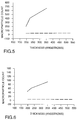
- Example 1-3 an undoped 46 cm2 silicon wafer, Si(100), was placed in the cathodic arc vacuum chamber, Ar+ sputter cleaned, and exposed to the carbon plasma produced by a SIGRADUR G vitreous carbon cathode (available from Sigri Corporation, Somerville, N.J.) in the form of three 1.27 cm x 5.1 cm x o.4 cm plates forming a 1.27 cm x 1.2 cm rectangular cross-sectional area to produce diamond-like coatings of various thicknesses as set forth in Table 1. Photomicrographs were taken. Photomicrographs of the 530 ⁇ thick coating are shown in FIGS. 1 and 2. The macroparticle count was determined using the image analysis software. The macroparticle counts are shown in Table 1 and in FIGS. 5 and 6 (dashed lines).
- the macroparticle count is very low.
- the apparent macroparticles which are seen in the photomicrographs are believed to be due to debris, impurities in the system.
- the cathodic arc discharge is believed to be free of macroparticles.
- the diamond-like carbon coatings of Examples 1-3 were shown to be hydrogen free by Attenuated Total Reflection (ATR) Infrared spectroscopy. This was determined by comparing cathodic arc produced coatings with RF deposited diamond-like carbon coatings. The latter were made using a parallel plate PLASMATHERM Model PK 2480 RF plasma reactor with butadiene as the reactant gas. The ATR signal for cathodic arc produced diamond-like coatings was compared with samples known to contain a significant hydrogen content. The latter samples were deposited directly on germanium ATR crystals and absorption measurements in the 2800 cm-1 to 3200 cm-1 were made in a DIGILAB Model FTS-50 spectrometer using a SPECTRATECH ATR cell.
- ATR Attenuated Total Reflection
- the RF plasma deposited hydrogen films displayed a broad absorption band due to the C-H stretching vibrations.
- the spectrum for the cathodic arc produced diamond-like carbon films of Examples 1-3 were devoid of C-H stretching vibrations. It therefore can be concluded that unlike the hydrogenated diamond-like carbon film deposited by the RF plasma process, the diamond-like carbon film of the invention deposited by cathodic arc evaporation from an amorphous vitreous carbon cathode is truly non-hydrogenated.
- Electron Energy Loss Spectroscopy was used to determine the plasmon energy loss of the coatings utilizing standard electron spectroscopic apparatus.
- the plasmon energy loss is related to the structural properties of the film because it is proportional to the valence electron density which is proportional to the atom density.
- Diamond has a plasmon energy loss of 33 eV and polycrystalline graphite about 25 eV.
- Rother et al. Journal of Material Research, vol. 6, no. 1, January 1991, pg 101, measured the plasmon energy of diamond-like carbon films with various deposition techniques and found that cathodic arc produced films have a higher fraction of diamond bonding character with a plasmon energy of between 29 and 30 eV. Rother et al.
- the plasmon energy of the films of the present invention were measured in the reflective mode with a beam energy of about 2000 eV wherein the film does not have to be separated from the substrate and the loss energy was found to be about 29 eV.
- the macroparticle counts are shown in Table 1 and in FIGS. 5 and 6 (solid lines). As can be seen, these coatings have a high number of macroparticles and the number of macroparticles increases with increasing thickness. TABLE 1 Example Thickness Macroparticle Count 106X 426X 1 200 ⁇ 34 4 2 490 ⁇ 40 6 3 530 ⁇ 46 4 C1 200 ⁇ 200 17 C2 230 ⁇ 412 50 C3 350 ⁇ 665 83
- Example 4 a 46 cm2 silicon wafer, Si(100), was placed in the cathodic arc vacuum chamber, sputter cleaned, and exposed to the plasma produced by a 1.9 cm diameter pyrolytic graphite carbon cathode from BF Goodrich which is an oriented large-grained polycrystalline carbon material to produce a diamond-like coating about 420 ⁇ thick.
- the macroparticle count was determined by visually counting bright spots in a 426X Namarski photomicrograph and was found to be between about 30 and 50 for a 200 ⁇ m x 163 ⁇ m area.
- Comparative Example C4 a 46 cm2 silicon wafer, Si(100), was placed in the cathodic arc vacuum chamber, sputter cleaned, and exposed to the plasma produced by a 1.9 cm diameter carbon-carbon composite material of randomly oriented carbon fibers in a carbon matrix (available from BF Goodrich) to produce a diamond-like coating about 500 ⁇ thick.
- the macroparticle count in three diamond-like carbon coatings was determined by counting bright spots in a 426X dark field photomicrograph and was found to be between 200 to 350 over a 200 ⁇ m x 163 ⁇ m area.
Abstract
Description
- The present invention relates to a method for producing diamond-like coatings and the coated articles made thereby.
- Amorphous carbon films having diamond-like properties of extreme hardness, extremely low electrical conductivity, low coefficients of friction, and optical transparency over a wide range of wavelengths, have widespread applications as optical coatings, low friction, anti-corrosion coatings and wear-resistant coatings and in various other applications such as surface finishing and in semiconductor manufacturing.
- Diamond-like carbon is a non-crystalline, or amorphous, material having two types of carbon-carbon bonds, i.e., hexagonal graphite bonds (sp²) and tetrahedral diamond bonds (sp³). Thus, diamond-like carbon has both limited long range order and two types of short range order.
- Diamond-like carbon may be hydrogenated or non-hydrogenated. Hydrogenated diamond-like carbon is produced from a hydrocarbon gas mixture using various energy sources, e.g., DC discharge, microwave and RF energy, oxyacetylene torches, and hot filaments. Non-hydrogenated diamond-like coatings can be produced using magnetron sputtering, electron beam evaporation, laser ablation and mass filtered carbon-ion beam deposition techniques, each of which has a very low deposition rate. Each method for producing the non-hydrogenated diamond-like carbon produces a hard carbon coating but the coatings have differing sp³/sp² bond ratios and, thus, the structural and physical characteristics differ.
- The sp³/sp² bond ratio can be estimated from the plasmon energy determined by electron energy loss spectroscopy. The plasmon energy is proportional to the atom density and diamond has a greater atom density and plasmon energy than graphite. Polycrystalline graphite has a plasmon energy loss of about 25 electron volts (eV). Diamond has a plasmon energy loss of about 33 eV. Non-hydrogenated diamond-like carbon has a plasmon energy loss between about 26 and 32 eV, the higher plasmon energies corresponding to higher atom densities which are believed to be due to an increased sp³ bonding component.
- Hydrogen-free non-crystalline diamond-like carbon coatings can also be produced using cathodic arc plasma deposition, a process which provides high deposition rates and allows control over the incident ion kinetic energy and the substrate temperatures. The sp³/sp² bond ratio is believed to be dependent on the incident ion kinetic energy. Cathodic arc plasma deposition can produce diamond-like carbon coatings with higher plasmon energies than alternative processes, thus, yielding higher sp³/sp² bond ratios.
- A cathodic arc discharge occurs when a high current power source is connected between two sufficiently conductive electrodes and the electrodes are momentarily in contact, either physically or by another discharge. Arc spots form on the cathode surface as the electrodes are separated. These small, luminous regions are often very mobile and move rapidly over the cathode surface. Due to the high current density contained in each spot, rapid ebullition of the cathode material occurs, and this plasma material can be confined, transported using magnetic fields and deposited on substrates. The current density at each spot can reach 100,000 amperes per square centimeter and this contributes to the ionization of much of the outflowing vapor.
- One of the major problems associated with cathodic arc discharges is the production of macroparticles. Macroparticles are droplets or solid particles of the consumable cathode which range in size from about 0.1 micron to greater than about 50 microns, most being between about 0.5 and 20 microns. These macro particles are deposited with the plasma to produce unwanted particles in the final coating. Macroparticle production is particularly undesirable for diamond-like carbon coatings because they are graphite and become embedded in the diamond-like carbon coating. Much attention has been given to the removal of these particles.
- U.S. Pat. No. 4,452,686 (Axenov et al.) describes one means of macroparticle removal via filtration. A cylindrically shaped current coil and a central axially mounted, football-shaped coil produce a magnetic field that guides the plasma around the central coil and through the plasma guide system. Macroparticles, which are much heavier than the plasma particles are not guided by the magnetic field and, thus, are blocked by the central coil. Downstream, the plasma macroparticle density is significantly reduced.
- I.I. Aksenov et al., "Transport of Plasma Streams in a Curvilinear Plasma Optics System", Soviet Journal Physics, 4(4), July-August 1978, pp. 425-428, describes a vacuum apparatus using curvilinear magnetic and electric fields to steer and focus the plasma and remove macroparticles from the plasma stream.
- Although such filtration means do reduce the macroparticle density in the coatings, they do not completely remove all macroparticles. Typically, the larger macroparticles are filtered, but the submicron particles are not completely filtered. This can occur as the submicron particles bounce around in the vacuum system. This can also result from momentum transfer from the plasma to the particles. Furthermore, plasma filters typically reduce the plasma flux by 30 to 50 percent, leading to reduced deposition rates.
- The present invention provides a method for producing a diamond-like carbon coating comprising the steps of providing a substrate to be coated, providing a cathode of vitreous carbon or pyrolytic graphite and initiating a cathodic arc discharge with the arc spot on the cathode surface and directing the resulting carbon plasma toward the substrate to form a coating on said substrate, said coating being substantially macroparticle free. The discharge may optionally be carried out in a magnetic field. The present invention overcomes the problem of macroparticles in diamond-like carbon coatings produced using a cathodic arc generator. The method of the presetn invention produces high quality, non-hydrogenated diamond-like coatings at high deposition rates.
- The present invention utilizes the cathodic arc process to produce non-hydrogenated, non-crystalline, diamond-like carbon coatings and films which are essentially macroparticle free. Unlike the prior art where the removal or filtration of the macroparticles was of prime concern, the present invention utilizes a cathodic arc carbon cathode material which does not generate macroparticles in the plasma discharge.
- FIG. 1 is a photomicrograph of the coating of Example 3 at 106X.
- FIG. 2 is a photomicrograph of the coating of Example 3 at 426X.
- FIG. 3 is a photomicrograph of the coating of Comparative Example 3 at 106X.
- FIG. 4 is a photomicrograph of the coating of Comparative Example 3 at 426X.
- FIG. 5 is a graph showing the relation between macroparticle count and coating thickness at 106X for Examples 1-3 (dashed line) and Comparative Examples C1-C3 (solid line).
- FIG. 6 is a graph showing the relation between macroparticle count and coating thickness at 426X for Examples 1-3 (dashed line) and Comparative Examples C1-C3 (solid line).
- The cathodic arc discharge coating process can be carried out under vacuum at pressues of, e.g., less than 10⁻³ Torr, at ambient conditions, e.g., room temperature of 20-25°C, in an inert atmosphere such as, for example, argon, or in a reactive atmosphere such as hydrogen or oxygen. The preferred mode is without gas flowing into the chamber. A cooled substrate holder may be preferred to keep the substrate at room temperature of slightly below room temperature when large plasma fluxes are produced.
- The cathode and, optionally, the anode can be electrically isolated from the vacuum chamber and electrically connected by a DC high current power source such as a welding power supply, i.e., continuous DC arc discharge. Alternatively, the arc discharge can be powered by a capacitor to produce a pulsed arc discharge.
- The cathodic arc discharge can be ignited by various means such as, for example, a mechanical striker, thin film ablation, high voltage spark discharge or a focused laser beam.
- The arc voltage is preferably between about 20 to 60 volts, more preferably between about 20 and 35 volts. The arc current is preferably greater than about 50 amps, more preferably greater than about 75 amps. The substrate surface temperature is preferably below about 200°C, and can be reduced by cooling.
- The carbon coating produced by the method of the present invention preferably has a plasmon energy loss of at least about 26 eV, more preferably at least about 29 eV.
- The cathodic arc apparatus used in the present invention was similar to that described in U.S. Pat. No. 3,836,451 (Snaper) which is incorporated herein by reference. A water-cooled copper block held the cathode. The cathode and anode were each electrically isolated from the vacuum chamber and connected to a DC welding power supply (INTELLIWELD 650, available from Miller Welding Co.) modified to produce an open circuit voltage of 95V. The vacuum vessel was 0.4 m in diameter and 1 m long and pumping was by an oil diffusion pump. The base pressure was between about 1·10⁻⁶ and 5·10⁻⁶ Torr. No inert or reactive gas was flowing into the system during the arc discharge. The power supply was operated in a constant current mode at 100 amps arc current. The open circuit voltage for the power supply was about 95 volts. The geometry and B field strength produced an arc voltage of about 25 to 35 volts. The cathodic arc discharge was operated in an intermittent manner. The discharge was maintained at 100 amps for 5.5 seconds then, after a 5 second pause, the cathodic arc discharge was reignited.
- The cathodic arc discharge was ignited by a mechanical striker. The striker was moved into momentary contact with both the cathode and anode and, as the striker was separated from the cathode surface, a plasma discharge was formed which moved outward from the cathode surface.
- The plasma discharge was collected and transported by magnetic fields created by two electromagnetic coils, spaced approximately 35 cm apart. The electromagnetic coil nearest the cathode was operated with 10 amps while the coil nearer the sample was operated with 2 amps. This geometry created a stronger magnetic field inside the coils and a weaker field between the coils. Consequently, the plasma expanded between the coils. In addition to a cooled cylindrical copper anode near the cathode, a cylindrically shaped stainless steel screen was placed within and coaxial to the vacuum chamber. This allowed a lower arc voltage of about 25 to 35 volts to be maintained even when large magnetic fields were applied near the cathode. This geometry allowed electrons in the plasma to follow magnetic field lines to the anode i.e., to follow a low voltage path. This resulted in a more stable discharge.
- The substrates used were undoped 7.6 cm diameter silicon wafers. The wafers were held onto the face of a water-cooled sample holder with a 5 cm diameter face which was electrically isolated from ground. The wafers effectively hid the sample holder from the plasma flux. A bias voltage of - 15 volts relative to the chamber was applied for each sample. Immediately prior to the cathodic arc discharge, the silicon wafer was sputtered clean with 1500 eV Ar⁺ ions incident at about a 60° angle relative to the surface normal. A Kauffman type ion source (available from Commonwealth Scientific Co.) was used with argon gas flowing into the back of the ion source. The argon flow rate was sufficient to increase the system pressure to about 7·10⁻⁴ Torr while the diffusion pump continued to pump on the system. The sputter cleaning cycle lasted for about 5 to 5.5 minutes.
- During the cathodic arc discharge the current to the sample and passing through the sample bias power supply was monitored since it is equal to the carbon ion current impinging on to the sample and sample holder. The thickness of the coating was controlled by integrating the carbon ion current to the sample. This was accomplished by transforming the carbon ion current into a voltage by measuring the voltage drop across a 4 ohm resistor.
- The diamond-like carbon coatings of the following examples were examined for macroparticles using a NICON MEASURESCOPE, Model UM-2, optical microscope. Macroparticles were readily visible as bright spots on a dark background when imaged in a dark field mode. Photomicrographs were obtained at magnifications of 106X and 426X. Two methods were used to measure the macroparticle density from photographs of the deposited films.
- An Advanced Image Analysis System was used to count the number of macroparticles in a region of the surface on the photomicrographs. The analysis area examined was 200 µm x 162 µm for the 426X photomicrographs and 804 µm x 651 µm for the 106X photomicrographs. Preferably, there are less than about 10 macroparticles in the 426X analysis area and less than about 100 macroparticles in the 106X analysis area, more preferably less than 50 macroparticles in the 106X analysis area.
- In each of Examples 1-3, an undoped 46 cm² silicon wafer, Si(100), was placed in the cathodic arc vacuum chamber, Ar⁺ sputter cleaned, and exposed to the carbon plasma produced by a SIGRADUR G vitreous carbon cathode (available from Sigri Corporation, Somerville, N.J.) in the form of three 1.27 cm x 5.1 cm x o.4 cm plates forming a 1.27 cm x 1.2 cm rectangular cross-sectional area to produce diamond-like coatings of various thicknesses as set forth in Table 1. Photomicrographs were taken. Photomicrographs of the 530 Å thick coating are shown in FIGS. 1 and 2. The macroparticle count was determined using the image analysis software. The macroparticle counts are shown in Table 1 and in FIGS. 5 and 6 (dashed lines).
- As can be seen, the macroparticle count is very low. The apparent macroparticles which are seen in the photomicrographs are believed to be due to debris, impurities in the system. The cathodic arc discharge is believed to be free of macroparticles.
- The diamond-like carbon coatings of Examples 1-3 were shown to be hydrogen free by Attenuated Total Reflection (ATR) Infrared spectroscopy. This was determined by comparing cathodic arc produced coatings with RF deposited diamond-like carbon coatings. The latter were made using a parallel plate PLASMATHERM Model PK 2480 RF plasma reactor with butadiene as the reactant gas. The ATR signal for cathodic arc produced diamond-like coatings was compared with samples known to contain a significant hydrogen content. The latter samples were deposited directly on germanium ATR crystals and absorption measurements in the 2800 cm-1 to 3200 cm-1 were made in a DIGILAB Model FTS-50 spectrometer using a SPECTRATECH ATR cell. The RF plasma deposited hydrogen films displayed a broad absorption band due to the C-H stretching vibrations. The spectrum for the cathodic arc produced diamond-like carbon films of Examples 1-3 were devoid of C-H stretching vibrations. It therefore can be concluded that unlike the hydrogenated diamond-like carbon film deposited by the RF plasma process, the diamond-like carbon film of the invention deposited by cathodic arc evaporation from an amorphous vitreous carbon cathode is truly non-hydrogenated.
- Standard Auger analysis of the films of Examples 1-3 indicated a carbon component of 97 percent or more with oxygen being the major trace impurity which was usually concentrated at the substrate/coating interface.
- Electron Energy Loss Spectroscopy (EELS) was used to determine the plasmon energy loss of the coatings utilizing standard electron spectroscopic apparatus. The plasmon energy loss is related to the structural properties of the film because it is proportional to the valence electron density which is proportional to the atom density. Diamond has a plasmon energy loss of 33 eV and polycrystalline graphite about 25 eV. Rother et al., Journal of Material Research, vol. 6, no. 1, January 1991, pg 101, measured the plasmon energy of diamond-like carbon films with various deposition techniques and found that cathodic arc produced films have a higher fraction of diamond bonding character with a plasmon energy of between 29 and 30 eV. Rother et al. measured the plasmon energy of their films in the transmission mode which requires the film to be separated from the substrate and very high incident electron energies must be used. The plasmon energy of the films of the present invention were measured in the reflective mode with a beam energy of about 2000 eV wherein the film does not have to be separated from the substrate and the loss energy was found to be about 29 eV.
- In each of Comparative Examples C1-C3, a 46 cm² silicon wafer, Si(100), was placed in the cathodic arc vacuum chamber, sputter cleaned, and exposed to the cathodic arc carbon plasma produced from a 1.9 cm diameter POCO SFG-2 graphite carbon cathode (available from Poco Graphite, Inc. a Unocal Company, Decatur, TX.) which is an ultra-fine grained and ultra pure material with 18 percent porosity to produce diamond-like coatings of various thicknesses as set forth in Table 1. Photomicrographs were taken. Photomicrographs of the 350 Å thick coating are shown in FIGS. 3 and 4. The macroparticle count was determined using the image analysis software. The macroparticle counts are shown in Table 1 and in FIGS. 5 and 6 (solid lines). As can be seen, these coatings have a high number of macroparticles and the number of macroparticles increases with increasing thickness.
TABLE 1 Example Thickness Macroparticle Count 106X 426X 1 200Å 34 4 2 490Å 40 6 3 530Å 46 4 C1 200Å 200 17 C2 230Å 412 50 C3 350Å 665 83 - In Example 4, a 46 cm² silicon wafer, Si(100), was placed in the cathodic arc vacuum chamber, sputter cleaned, and exposed to the plasma produced by a 1.9 cm diameter pyrolytic graphite carbon cathode from BF Goodrich which is an oriented large-grained polycrystalline carbon material to produce a diamond-like coating about 420 Å thick. The macroparticle count was determined by visually counting bright spots in a 426X Namarski photomicrograph and was found to be between about 30 and 50 for a 200µm x 163µm area.
- In Comparative Example C4, a 46 cm² silicon wafer, Si(100), was placed in the cathodic arc vacuum chamber, sputter cleaned, and exposed to the plasma produced by a 1.9 cm diameter carbon-carbon composite material of randomly oriented carbon fibers in a carbon matrix (available from BF Goodrich) to produce a diamond-like coating about 500 Å thick. The macroparticle count in three diamond-like carbon coatings was determined by counting bright spots in a 426X dark field photomicrograph and was found to be between 200 to 350 over a 200µm x 163µm area.
- The various modifications and alterations of this invention will be apparent to those skilled in the art without department from the scope and spirit of this invention and this invention should not be restricted to that set forth herein for illustrative purposes.
Claims (7)
- A method for producing a diamond-like carbon coating comprising the steps of providing a substrate to be coated, providing a cathode of vitreous carbon or a pyrolytic graphite cathode and initiating a substantially macroparticle free cathodic arc discharge with the arc spot on the cathode surface and directing the resulting carbon plasma toward the substrate to form a coating on said substrate, said coating being substantially macroparticle free.
- The method of claim 1 wherein said cathodic arc discharge is powered by a DC high current power source.
- The method of claim 1 wherein said cathodic arc discharge is powered by a capacitor to produce a pulsed arc discharge.
- The method of claim 1, 2 or 3 wherein the arc voltage is between about 20 to 60 volts.
- The method of any of claims 1 to 4 wherein the arc current is at least about 50 amps.
- The method of any of claims 1 to 5 wherein said discharge is carried out in a magnetic field.
- Coated article producible with the method of any one of claims 1 to 6.
Applications Claiming Priority (2)
| Application Number | Priority Date | Filing Date | Title |
|---|---|---|---|
| US149292 | 1993-11-09 | ||
| US08/149,292 US5401543A (en) | 1993-11-09 | 1993-11-09 | Method for forming macroparticle-free DLC films by cathodic arc discharge |
Publications (2)
| Publication Number | Publication Date |
|---|---|
| EP0652301A1 true EP0652301A1 (en) | 1995-05-10 |
| EP0652301B1 EP0652301B1 (en) | 1998-01-07 |
Family
ID=22529604
Family Applications (1)
| Application Number | Title | Priority Date | Filing Date |
|---|---|---|---|
| EP94115881A Expired - Lifetime EP0652301B1 (en) | 1993-11-09 | 1994-10-07 | Method for producing diamond-like coatings |
Country Status (4)
| Country | Link |
|---|---|
| US (1) | US5401543A (en) |
| EP (1) | EP0652301B1 (en) |
| JP (1) | JPH07188916A (en) |
| DE (1) | DE69407734T2 (en) |
Cited By (11)
| Publication number | Priority date | Publication date | Assignee | Title |
|---|---|---|---|---|
| DE10214781A1 (en) * | 2002-04-03 | 2003-10-30 | Univ Jw Goethe Frankfurt Main | Infrared spectrometry device, especially for the spectrometry of aqueous systems, comprises an attenuated total reflection body and an infrared source with the ATR body configured to provide total internal reflection |
| DE10218823A1 (en) * | 2002-04-26 | 2003-11-20 | Schott Glas | Target material used e.g. in the manufacture of diamond-like carbon layers on a substrate contains glass-like carbon |
| WO2006021275A1 (en) * | 2004-08-26 | 2006-03-02 | Schaeffler Kg | Wear-resistant coating and method for producing the same |
| US7273655B2 (en) | 1999-04-09 | 2007-09-25 | Shojiro Miyake | Slidably movable member and method of producing same |
| US7650976B2 (en) | 2003-08-22 | 2010-01-26 | Nissan Motor Co., Ltd. | Low-friction sliding member in transmission, and transmission oil therefor |
| US7812312B2 (en) | 2002-04-03 | 2010-10-12 | Johann Wolfgang Goethe-Universitaet | Infrared measuring device, especially for the spectrometry of aqueous systems, preferably multiple component systems |
| US8096205B2 (en) | 2003-07-31 | 2012-01-17 | Nissan Motor Co., Ltd. | Gear |
| US8152377B2 (en) | 2002-11-06 | 2012-04-10 | Nissan Motor Co., Ltd. | Low-friction sliding mechanism |
| US8206035B2 (en) | 2003-08-06 | 2012-06-26 | Nissan Motor Co., Ltd. | Low-friction sliding mechanism, low-friction agent composition and method of friction reduction |
| DE102011105645A1 (en) | 2011-06-07 | 2012-12-13 | Oerlikon Trading Ag, Trübbach | Method for reactive stripping of tetrahedral carbon layer on semiconductor wafer of e.g. chipping tool, involves performing plasma discharge process in vacuum chamber to support chemical reaction for stripping of carbon on substrate |
| US9230778B2 (en) | 2011-06-07 | 2016-01-05 | Oerlikon Surface Solutions Ag, Trubbach | Method for removing hard carbon layers |
Families Citing this family (70)
| Publication number | Priority date | Publication date | Assignee | Title |
|---|---|---|---|---|
| US6083570A (en) * | 1987-03-31 | 2000-07-04 | Lemelson; Jerome H. | Synthetic diamond coatings with intermediate amorphous metal bonding layers and methods of applying such coatings |
| CA2065581C (en) | 1991-04-22 | 2002-03-12 | Andal Corp. | Plasma enhancement apparatus and method for physical vapor deposition |
| US5580429A (en) * | 1992-08-25 | 1996-12-03 | Northeastern University | Method for the deposition and modification of thin films using a combination of vacuum arcs and plasma immersion ion implantation |
| US5626963A (en) * | 1993-07-07 | 1997-05-06 | Sanyo Electric Co., Ltd. | Hard-carbon-film-coated substrate and apparatus for forming the same |
| US5691010A (en) * | 1993-10-19 | 1997-11-25 | Sanyo Electric Co., Ltd. | Arc discharge plasma CVD method for forming diamond-like carbon films |
| US5643343A (en) * | 1993-11-23 | 1997-07-01 | Selifanov; Oleg Vladimirovich | Abrasive material for precision surface treatment and a method for the manufacturing thereof |
| US5551959A (en) * | 1994-08-24 | 1996-09-03 | Minnesota Mining And Manufacturing Company | Abrasive article having a diamond-like coating layer and method for making same |
| US5711773A (en) * | 1994-11-17 | 1998-01-27 | Plasmoteg Engineering Center | Abrasive material for precision surface treatment and a method for the manufacturing thereof |
| DE19502568C1 (en) * | 1995-01-27 | 1996-07-25 | Fraunhofer Ges Forschung | Hard, amorphous, hydrogen-free C-layers and process for their production |
| US5616372A (en) * | 1995-06-07 | 1997-04-01 | Syndia Corporation | Method of applying a wear-resistant diamond coating to a substrate |
| US5688557A (en) * | 1995-06-07 | 1997-11-18 | Lemelson; Jerome H. | Method of depositing synthetic diamond coatings with intermediates bonding layers |
| US5712000A (en) * | 1995-10-12 | 1998-01-27 | Hughes Aircraft Company | Large-scale, low pressure plasma-ion deposition of diamondlike carbon films |
| US5738768A (en) * | 1995-10-31 | 1998-04-14 | Caterpillar Inc. | Process for reducing particle defects in arc vapor deposition coatings |
| US5760496A (en) * | 1996-04-23 | 1998-06-02 | The United States Of America As Represented By The Secretary Of The Air Force | Inverse-pinch voltage pulse generator |
| DE19621855C2 (en) | 1996-05-31 | 2003-03-27 | Univ Dresden Tech | Process for producing metallizations on semiconductor bodies using a pulsed vacuum arc evaporator |
| CA2207878A1 (en) * | 1996-06-20 | 1997-12-20 | Qqc, Inc. | Glassy carbon coatings having water repellant and corrosion-, erosion-, and wear-resistant characteristics |
| DE19628102A1 (en) * | 1996-07-12 | 1998-01-15 | Bayerische Motoren Werke Ag | Vacuum coating system with a coating chamber and at least one source chamber |
| US5902462A (en) * | 1997-03-27 | 1999-05-11 | Krauss; Alan R. | Filtered cathodic arc deposition apparatus and method |
| RU2114210C1 (en) * | 1997-05-30 | 1998-06-27 | Валерий Павлович Гончаренко | Process of formation of carbon diamond-like coat in vacuum |
| US6974629B1 (en) | 1999-08-06 | 2005-12-13 | Cardinal Cg Company | Low-emissivity, soil-resistant coating for glass surfaces |
| US6964731B1 (en) | 1998-12-21 | 2005-11-15 | Cardinal Cg Company | Soil-resistant coating for glass surfaces |
| US6660365B1 (en) | 1998-12-21 | 2003-12-09 | Cardinal Cg Company | Soil-resistant coating for glass surfaces |
| CA2256847A1 (en) * | 1998-12-22 | 2000-06-22 | Munther Kandah | Particle-free cathodic arc carbon ion source |
| JP2004503680A (en) * | 2000-07-17 | 2004-02-05 | コモンウェルス サイエンティフィック アンド インダストリアル リサーチ オーガニゼーション | Manufacture of carbon and carbon-based materials |
| US6921579B2 (en) * | 2000-09-11 | 2005-07-26 | Cardinal Cg Company | Temporary protective covers |
| US6821189B1 (en) | 2000-10-13 | 2004-11-23 | 3M Innovative Properties Company | Abrasive article comprising a structured diamond-like carbon coating and method of using same to mechanically treat a substrate |
| JP4793531B2 (en) * | 2001-07-17 | 2011-10-12 | 住友電気工業株式会社 | Amorphous carbon coating, method for producing amorphous carbon coating, and coating member for amorphous carbon coating |
| US6902813B2 (en) * | 2001-09-11 | 2005-06-07 | Cardinal Cg Company | Hydrophilic surfaces carrying temporary protective covers |
| JP2004138128A (en) | 2002-10-16 | 2004-05-13 | Nissan Motor Co Ltd | Sliding member for automotive engine |
| US6904935B2 (en) * | 2002-12-18 | 2005-06-14 | Masco Corporation Of Indiana | Valve component with multiple surface layers |
| US7866342B2 (en) | 2002-12-18 | 2011-01-11 | Vapor Technologies, Inc. | Valve component for faucet |
| US8220489B2 (en) | 2002-12-18 | 2012-07-17 | Vapor Technologies Inc. | Faucet with wear-resistant valve component |
| US7866343B2 (en) | 2002-12-18 | 2011-01-11 | Masco Corporation Of Indiana | Faucet |
| US8555921B2 (en) * | 2002-12-18 | 2013-10-15 | Vapor Technologies Inc. | Faucet component with coating |
| JP3891433B2 (en) * | 2003-04-15 | 2007-03-14 | 日産自動車株式会社 | Fuel injection valve |
| EP1479946B1 (en) * | 2003-05-23 | 2012-12-19 | Nissan Motor Co., Ltd. | Piston for internal combustion engine |
| EP1482190B1 (en) * | 2003-05-27 | 2012-12-05 | Nissan Motor Company Limited | Rolling element |
| JP2005008851A (en) * | 2003-05-29 | 2005-01-13 | Nissan Motor Co Ltd | Cutting oil for cutting tool coated with hard carbon thin film, and cutting tool coated with hard carbon thin film |
| JP2004360649A (en) | 2003-06-06 | 2004-12-24 | Nissan Motor Co Ltd | Piston pin for engine |
| JP2005054617A (en) * | 2003-08-08 | 2005-03-03 | Nissan Motor Co Ltd | Valve system |
| JP4973971B2 (en) * | 2003-08-08 | 2012-07-11 | 日産自動車株式会社 | Sliding member |
| JP4117553B2 (en) * | 2003-08-13 | 2008-07-16 | 日産自動車株式会社 | Chain drive |
| EP1507088B1 (en) | 2003-08-13 | 2007-08-29 | Nissan Motor Company, Limited | Structure for connecting piston to crankshaft |
| JP4539205B2 (en) | 2003-08-21 | 2010-09-08 | 日産自動車株式会社 | Refrigerant compressor |
| US7771821B2 (en) * | 2003-08-21 | 2010-08-10 | Nissan Motor Co., Ltd. | Low-friction sliding member and low-friction sliding mechanism using same |
| US7294404B2 (en) * | 2003-12-22 | 2007-11-13 | Cardinal Cg Company | Graded photocatalytic coatings |
| US20050249983A1 (en) * | 2004-05-06 | 2005-11-10 | Seagate Technology Llc | Thickness gradient protective overcoat layers by filtered cathodic arc deposition |
| DE602005003234T2 (en) * | 2004-07-12 | 2008-08-28 | Cardinal Cg Co., Eden Prairie | MAINTENANCE-FREE COATINGS |
| US20060059688A1 (en) * | 2004-09-22 | 2006-03-23 | Tseng Shao C | Method for producing a dynamic fluid bearing with high rotation precision and high hardness |
| US8092660B2 (en) * | 2004-12-03 | 2012-01-10 | Cardinal Cg Company | Methods and equipment for depositing hydrophilic coatings, and deposition technologies for thin films |
| US7923114B2 (en) * | 2004-12-03 | 2011-04-12 | Cardinal Cg Company | Hydrophilic coatings, methods for depositing hydrophilic coatings, and improved deposition technology for thin films |
| US8241468B2 (en) * | 2004-12-13 | 2012-08-14 | United Technologies Corporation | Method and apparatus for cathodic arc deposition of materials on a substrate |
| US20070026205A1 (en) * | 2005-08-01 | 2007-02-01 | Vapor Technologies Inc. | Article having patterned decorative coating |
| WO2007124291A2 (en) | 2006-04-19 | 2007-11-01 | Cardinal Cg Company | Opposed functional coatings having comparable single surface reflectances |
| US20100131023A1 (en) * | 2006-06-21 | 2010-05-27 | Benedict James Costello | Implantable medical devices comprising cathodic arc produced structures |
| US20080011599A1 (en) | 2006-07-12 | 2008-01-17 | Brabender Dennis M | Sputtering apparatus including novel target mounting and/or control |
| US7414547B2 (en) * | 2006-12-22 | 2008-08-19 | 3M Innovative Properties Company | Method and system for calibrating a rotary encoder and making a high resolution rotary encoder |
| EP3236524A1 (en) | 2007-02-14 | 2017-10-25 | Proteus Digital Health, Inc. | In-body power source having high surface area electrode |
| WO2008149824A1 (en) * | 2007-06-01 | 2008-12-11 | Onward Ceramic Coating Co., Ltd. | Dlc-coated tool |
| EP2261186B1 (en) * | 2007-09-14 | 2017-11-22 | Cardinal CG Company | Low maintenance coating technology |
| JP2009283107A (en) * | 2008-05-26 | 2009-12-03 | Fuji Electric Device Technology Co Ltd | Protection film mainly including tetrahedral amorphous carbon film and magnetic recording medium having the same |
| JP5780704B2 (en) | 2010-01-19 | 2015-09-16 | 株式会社リケン | Hydrogen-containing amorphous hard carbon coated member |
| WO2012073869A1 (en) * | 2010-11-30 | 2012-06-07 | 株式会社野村鍍金 | Conductive hard carbon film, and film forming method therefor |
| US9514932B2 (en) | 2012-08-08 | 2016-12-06 | Applied Materials, Inc. | Flowable carbon for semiconductor processing |
| EP2949779A4 (en) * | 2013-01-22 | 2016-10-05 | Nissin Electric Co Ltd | Plasma device, carbon thin film manufacturing method and coating method using plasma device |
| US20140322431A1 (en) * | 2013-04-24 | 2014-10-30 | HGST Netherlands B.V. | Predicting a characteristic of an overcoat |
| JP6414404B2 (en) * | 2014-07-18 | 2018-10-31 | 日新電機株式会社 | Cathode member and plasma apparatus using the same |
| EP3387163B1 (en) | 2015-12-11 | 2020-04-29 | Cardinal CG Company | Method of coating both sides of a substrate |
| CZ201660A3 (en) | 2016-02-05 | 2017-03-22 | Platit A.S. | A method of applying a wear-resistant DLC layer |
| EP3541762B1 (en) | 2016-11-17 | 2022-03-02 | Cardinal CG Company | Static-dissipative coating technology |
Citations (3)
| Publication number | Priority date | Publication date | Assignee | Title |
|---|---|---|---|---|
| EP0156069A2 (en) * | 1983-11-28 | 1985-10-02 | Kabushiki Kaisha Meidensha | Diamond-like thin film and method for making the same |
| EP0280315A2 (en) * | 1987-02-26 | 1988-08-31 | Nissin Electric Company, Limited | Method of forming a diamond film |
| EP0440326A1 (en) * | 1990-01-29 | 1991-08-07 | BAUSCH & LOMB INCORPORATED | Method of depositing diamond-like film onto a substrate having a low melting temperature |
Family Cites Families (7)
| Publication number | Priority date | Publication date | Assignee | Title |
|---|---|---|---|---|
| US3836451A (en) * | 1968-12-26 | 1974-09-17 | A Snaper | Arc deposition apparatus |
| US4452686A (en) * | 1982-03-22 | 1984-06-05 | Axenov Ivan I | Arc plasma generator and a plasma arc apparatus for treating the surfaces of work-pieces, incorporating the same arc plasma generator |
| US5087959A (en) * | 1987-03-02 | 1992-02-11 | Microwave Technology, Inc. | Protective coating useful as a passivation layer for semiconductor devices |
| DE3712205A1 (en) * | 1987-04-10 | 1988-10-20 | Detlev Dipl Chem Dr Repenning | Process for producing layers having very hard diamond-like and/or low-friction properties |
| US5098737A (en) * | 1988-04-18 | 1992-03-24 | Board Of Regents The University Of Texas System | Amorphic diamond material produced by laser plasma deposition |
| US5254237A (en) * | 1991-03-01 | 1993-10-19 | Snaper Alvin A | Plasma arc apparatus for producing diamond semiconductor devices |
| US5281321A (en) * | 1991-08-20 | 1994-01-25 | Leybold Aktiengesellschaft | Device for the suppression of arcs |
-
1993
- 1993-11-09 US US08/149,292 patent/US5401543A/en not_active Expired - Lifetime
-
1994
- 1994-10-07 EP EP94115881A patent/EP0652301B1/en not_active Expired - Lifetime
- 1994-10-07 DE DE69407734T patent/DE69407734T2/en not_active Expired - Fee Related
- 1994-11-04 JP JP6293689A patent/JPH07188916A/en active Pending
Patent Citations (3)
| Publication number | Priority date | Publication date | Assignee | Title |
|---|---|---|---|---|
| EP0156069A2 (en) * | 1983-11-28 | 1985-10-02 | Kabushiki Kaisha Meidensha | Diamond-like thin film and method for making the same |
| EP0280315A2 (en) * | 1987-02-26 | 1988-08-31 | Nissin Electric Company, Limited | Method of forming a diamond film |
| EP0440326A1 (en) * | 1990-01-29 | 1991-08-07 | BAUSCH & LOMB INCORPORATED | Method of depositing diamond-like film onto a substrate having a low melting temperature |
Cited By (13)
| Publication number | Priority date | Publication date | Assignee | Title |
|---|---|---|---|---|
| US7273655B2 (en) | 1999-04-09 | 2007-09-25 | Shojiro Miyake | Slidably movable member and method of producing same |
| US7812312B2 (en) | 2002-04-03 | 2010-10-12 | Johann Wolfgang Goethe-Universitaet | Infrared measuring device, especially for the spectrometry of aqueous systems, preferably multiple component systems |
| DE10214781B4 (en) * | 2002-04-03 | 2006-11-16 | Johann Wolfgang Goethe-Universität Frankfurt am Main | FT-IR measuring device, in particular for the spectrometry of aqueous systems |
| DE10214781A1 (en) * | 2002-04-03 | 2003-10-30 | Univ Jw Goethe Frankfurt Main | Infrared spectrometry device, especially for the spectrometry of aqueous systems, comprises an attenuated total reflection body and an infrared source with the ATR body configured to provide total internal reflection |
| DE10218823A1 (en) * | 2002-04-26 | 2003-11-20 | Schott Glas | Target material used e.g. in the manufacture of diamond-like carbon layers on a substrate contains glass-like carbon |
| US8152377B2 (en) | 2002-11-06 | 2012-04-10 | Nissan Motor Co., Ltd. | Low-friction sliding mechanism |
| US8096205B2 (en) | 2003-07-31 | 2012-01-17 | Nissan Motor Co., Ltd. | Gear |
| US8206035B2 (en) | 2003-08-06 | 2012-06-26 | Nissan Motor Co., Ltd. | Low-friction sliding mechanism, low-friction agent composition and method of friction reduction |
| US7650976B2 (en) | 2003-08-22 | 2010-01-26 | Nissan Motor Co., Ltd. | Low-friction sliding member in transmission, and transmission oil therefor |
| WO2006021275A1 (en) * | 2004-08-26 | 2006-03-02 | Schaeffler Kg | Wear-resistant coating and method for producing the same |
| DE102011105645A1 (en) | 2011-06-07 | 2012-12-13 | Oerlikon Trading Ag, Trübbach | Method for reactive stripping of tetrahedral carbon layer on semiconductor wafer of e.g. chipping tool, involves performing plasma discharge process in vacuum chamber to support chemical reaction for stripping of carbon on substrate |
| WO2012167886A1 (en) | 2011-06-07 | 2012-12-13 | Oerlikon Trading Ag, Trübbach | Method for removing hard carbon layers |
| US9230778B2 (en) | 2011-06-07 | 2016-01-05 | Oerlikon Surface Solutions Ag, Trubbach | Method for removing hard carbon layers |
Also Published As
| Publication number | Publication date |
|---|---|
| DE69407734T2 (en) | 1998-07-02 |
| DE69407734D1 (en) | 1998-02-12 |
| EP0652301B1 (en) | 1998-01-07 |
| JPH07188916A (en) | 1995-07-25 |
| US5401543A (en) | 1995-03-28 |
Similar Documents
| Publication | Publication Date | Title |
|---|---|---|
| EP0652301B1 (en) | Method for producing diamond-like coatings | |
| US5098737A (en) | Amorphic diamond material produced by laser plasma deposition | |
| Wagal et al. | Diamond‐like carbon films prepared with a laser ion source | |
| US6544627B1 (en) | Method of producing recording media having protective overcoats of highly tetrahedral amorphous carbon | |
| US5458754A (en) | Plasma enhancement apparatus and method for physical vapor deposition | |
| Boxman et al. | Principles and applications of vacuum arc coatings | |
| US5433836A (en) | Arc source macroparticle filter | |
| US4336277A (en) | Transparent electrical conducting films by activated reactive evaporation | |
| Martin et al. | Ion-beam-deposited films produced by filtered arcevaporation | |
| EP0909445A1 (en) | Recording media having protective overcoats of highly tetrahedral amorphous carbon and methods for their production | |
| WO1997045834A9 (en) | Recording media having protective overcoats of highly tetrahedral amorphous carbon and methods for their production | |
| KR100343654B1 (en) | Cubic Boron Nitride Film Manufacturing Method | |
| Musil et al. | High‐rate magnetron sputtering | |
| Sundaram et al. | Deposition and X-ray photoelectron spectroscopy studies on sputtered cerium dioxide thin films | |
| Chhowalla et al. | Deposition of smooth tetrahedral amorphous carbon thin films using a cathodic arc without a macroparticle filter | |
| Arbilly et al. | Amorphous Si thin films prepared by vacuum arc deposition | |
| Ullmann et al. | Diamond-like amorphous carbon films prepared by rf sputtering in argon | |
| Takahashi et al. | Optical response of tin nitride thin films prepared by halide chemical vapor deposition under atmospheric pressure | |
| Grill | Ion beam reactively sputtered silicon nitride coatings | |
| Charrier et al. | Carbon films deposited by the physical vapour deposition focused-arc evaporation technique | |
| JPH04341558A (en) | Article with diamondlike protective film and its production | |
| Ogale et al. | Deposition of Diamond-Like and Other Special Coatings by Pulsed Laser Ablation and Their Post-Synthesis Processing | |
| Bewilogua et al. | Microhardness and structure of reactive ion‐plated chromium/carbon films | |
| RU2105379C1 (en) | Process of production of continuous film with diamond-like structure and gear for its implementation | |
| Ro et al. | Microstructure of gold films grown by ion induced deposition |
Legal Events
| Date | Code | Title | Description |
|---|---|---|---|
| PUAI | Public reference made under article 153(3) epc to a published international application that has entered the european phase |
Free format text: ORIGINAL CODE: 0009012 |
|
| AK | Designated contracting states |
Kind code of ref document: A1 Designated state(s): DE FR GB IT SE |
|
| 17P | Request for examination filed |
Effective date: 19950810 |
|
| 17Q | First examination report despatched |
Effective date: 19960115 |
|
| GRAG | Despatch of communication of intention to grant |
Free format text: ORIGINAL CODE: EPIDOS AGRA |
|
| GRAH | Despatch of communication of intention to grant a patent |
Free format text: ORIGINAL CODE: EPIDOS IGRA |
|
| GRAH | Despatch of communication of intention to grant a patent |
Free format text: ORIGINAL CODE: EPIDOS IGRA |
|
| GRAA | (expected) grant |
Free format text: ORIGINAL CODE: 0009210 |
|
| ITF | It: translation for a ep patent filed |
Owner name: PROROGA CONCESSA IN DATA: 11.02.98;BARZANO' E ZANA |
|
| AK | Designated contracting states |
Kind code of ref document: B1 Designated state(s): DE FR GB IT SE |
|
| REF | Corresponds to: |
Ref document number: 69407734 Country of ref document: DE Date of ref document: 19980212 |
|
| ET | Fr: translation filed | ||
| PGFP | Annual fee paid to national office [announced via postgrant information from national office to epo] |
Ref country code: SE Payment date: 19980918 Year of fee payment: 5 |
|
| PLBE | No opposition filed within time limit |
Free format text: ORIGINAL CODE: 0009261 |
|
| STAA | Information on the status of an ep patent application or granted ep patent |
Free format text: STATUS: NO OPPOSITION FILED WITHIN TIME LIMIT |
|
| 26N | No opposition filed | ||
| PG25 | Lapsed in a contracting state [announced via postgrant information from national office to epo] |
Ref country code: SE Free format text: THE PATENT HAS BEEN ANNULLED BY A DECISION OF A NATIONAL AUTHORITY Effective date: 19991030 |
|
| EUG | Se: european patent has lapsed |
Ref document number: 94115881.8 |
|
| REG | Reference to a national code |
Ref country code: GB Ref legal event code: IF02 |
|
| PGFP | Annual fee paid to national office [announced via postgrant information from national office to epo] |
Ref country code: GB Payment date: 20050928 Year of fee payment: 12 |
|
| PG25 | Lapsed in a contracting state [announced via postgrant information from national office to epo] |
Ref country code: IT Free format text: LAPSE BECAUSE OF NON-PAYMENT OF DUE FEES;WARNING: LAPSES OF ITALIAN PATENTS WITH EFFECTIVE DATE BEFORE 2007 MAY HAVE OCCURRED AT ANY TIME BEFORE 2007. THE CORRECT EFFECTIVE DATE MAY BE DIFFERENT FROM THE ONE RECORDED. Effective date: 20051007 |
|
| PGFP | Annual fee paid to national office [announced via postgrant information from national office to epo] |
Ref country code: FR Payment date: 20051017 Year of fee payment: 12 |
|
| PGFP | Annual fee paid to national office [announced via postgrant information from national office to epo] |
Ref country code: DE Payment date: 20061130 Year of fee payment: 13 |
|
| GBPC | Gb: european patent ceased through non-payment of renewal fee |
Effective date: 20061007 |
|
| REG | Reference to a national code |
Ref country code: FR Ref legal event code: ST Effective date: 20070629 |
|
| PG25 | Lapsed in a contracting state [announced via postgrant information from national office to epo] |
Ref country code: GB Free format text: LAPSE BECAUSE OF NON-PAYMENT OF DUE FEES Effective date: 20061007 |
|
| PG25 | Lapsed in a contracting state [announced via postgrant information from national office to epo] |
Ref country code: FR Free format text: LAPSE BECAUSE OF NON-PAYMENT OF DUE FEES Effective date: 20061031 |
|
| PG25 | Lapsed in a contracting state [announced via postgrant information from national office to epo] |
Ref country code: DE Free format text: LAPSE BECAUSE OF NON-PAYMENT OF DUE FEES Effective date: 20080501 |