EP0657931A1 - Semiconductor device and manufacturing method of the same - Google Patents
Semiconductor device and manufacturing method of the same Download PDFInfo
- Publication number
- EP0657931A1 EP0657931A1 EP94119251A EP94119251A EP0657931A1 EP 0657931 A1 EP0657931 A1 EP 0657931A1 EP 94119251 A EP94119251 A EP 94119251A EP 94119251 A EP94119251 A EP 94119251A EP 0657931 A1 EP0657931 A1 EP 0657931A1
- Authority
- EP
- European Patent Office
- Prior art keywords
- semiconductor chip
- fixing
- leads
- lead
- distal ends
- Prior art date
- Legal status (The legal status is an assumption and is not a legal conclusion. Google has not performed a legal analysis and makes no representation as to the accuracy of the status listed.)
- Granted
Links
Images


Classifications
-
- H—ELECTRICITY
- H01—ELECTRIC ELEMENTS
- H01L—SEMICONDUCTOR DEVICES NOT COVERED BY CLASS H10
- H01L23/00—Details of semiconductor or other solid state devices
- H01L23/48—Arrangements for conducting electric current to or from the solid state body in operation, e.g. leads, terminal arrangements ; Selection of materials therefor
-
- H—ELECTRICITY
- H01—ELECTRIC ELEMENTS
- H01L—SEMICONDUCTOR DEVICES NOT COVERED BY CLASS H10
- H01L24/00—Arrangements for connecting or disconnecting semiconductor or solid-state bodies; Methods or apparatus related thereto
- H01L24/01—Means for bonding being attached to, or being formed on, the surface to be connected, e.g. chip-to-package, die-attach, "first-level" interconnects; Manufacturing methods related thereto
-
- H—ELECTRICITY
- H01—ELECTRIC ELEMENTS
- H01L—SEMICONDUCTOR DEVICES NOT COVERED BY CLASS H10
- H01L23/00—Details of semiconductor or other solid state devices
- H01L23/48—Arrangements for conducting electric current to or from the solid state body in operation, e.g. leads, terminal arrangements ; Selection of materials therefor
- H01L23/488—Arrangements for conducting electric current to or from the solid state body in operation, e.g. leads, terminal arrangements ; Selection of materials therefor consisting of soldered or bonded constructions
- H01L23/495—Lead-frames or other flat leads
- H01L23/49503—Lead-frames or other flat leads characterised by the die pad
- H01L23/4951—Chip-on-leads or leads-on-chip techniques, i.e. inner lead fingers being used as die pad
-
- H—ELECTRICITY
- H01—ELECTRIC ELEMENTS
- H01L—SEMICONDUCTOR DEVICES NOT COVERED BY CLASS H10
- H01L23/00—Details of semiconductor or other solid state devices
- H01L23/48—Arrangements for conducting electric current to or from the solid state body in operation, e.g. leads, terminal arrangements ; Selection of materials therefor
- H01L23/488—Arrangements for conducting electric current to or from the solid state body in operation, e.g. leads, terminal arrangements ; Selection of materials therefor consisting of soldered or bonded constructions
- H01L23/495—Lead-frames or other flat leads
- H01L23/49503—Lead-frames or other flat leads characterised by the die pad
- H01L23/49513—Lead-frames or other flat leads characterised by the die pad having bonding material between chip and die pad
-
- H—ELECTRICITY
- H01—ELECTRIC ELEMENTS
- H01L—SEMICONDUCTOR DEVICES NOT COVERED BY CLASS H10
- H01L23/00—Details of semiconductor or other solid state devices
- H01L23/48—Arrangements for conducting electric current to or from the solid state body in operation, e.g. leads, terminal arrangements ; Selection of materials therefor
- H01L23/488—Arrangements for conducting electric current to or from the solid state body in operation, e.g. leads, terminal arrangements ; Selection of materials therefor consisting of soldered or bonded constructions
- H01L23/495—Lead-frames or other flat leads
- H01L23/49541—Geometry of the lead-frame
- H01L23/49548—Cross section geometry
- H01L23/49551—Cross section geometry characterised by bent parts
-
- H—ELECTRICITY
- H01—ELECTRIC ELEMENTS
- H01L—SEMICONDUCTOR DEVICES NOT COVERED BY CLASS H10
- H01L24/00—Arrangements for connecting or disconnecting semiconductor or solid-state bodies; Methods or apparatus related thereto
- H01L24/01—Means for bonding being attached to, or being formed on, the surface to be connected, e.g. chip-to-package, die-attach, "first-level" interconnects; Manufacturing methods related thereto
- H01L24/26—Layer connectors, e.g. plate connectors, solder or adhesive layers; Manufacturing methods related thereto
- H01L24/31—Structure, shape, material or disposition of the layer connectors after the connecting process
- H01L24/32—Structure, shape, material or disposition of the layer connectors after the connecting process of an individual layer connector
-
- H—ELECTRICITY
- H01—ELECTRIC ELEMENTS
- H01L—SEMICONDUCTOR DEVICES NOT COVERED BY CLASS H10
- H01L24/00—Arrangements for connecting or disconnecting semiconductor or solid-state bodies; Methods or apparatus related thereto
- H01L24/71—Means for bonding not being attached to, or not being formed on, the surface to be connected
- H01L24/72—Detachable connecting means consisting of mechanical auxiliary parts connecting the device, e.g. pressure contacts using springs or clips
-
- H—ELECTRICITY
- H01—ELECTRIC ELEMENTS
- H01L—SEMICONDUCTOR DEVICES NOT COVERED BY CLASS H10
- H01L24/00—Arrangements for connecting or disconnecting semiconductor or solid-state bodies; Methods or apparatus related thereto
- H01L24/90—Methods for connecting semiconductor or solid state bodies using means for bonding not being attached to, or not being formed on, the body surface to be connected, e.g. pressure contacts using springs or clips
-
- H—ELECTRICITY
- H01—ELECTRIC ELEMENTS
- H01L—SEMICONDUCTOR DEVICES NOT COVERED BY CLASS H10
- H01L2224/00—Indexing scheme for arrangements for connecting or disconnecting semiconductor or solid-state bodies and methods related thereto as covered by H01L24/00
- H01L2224/01—Means for bonding being attached to, or being formed on, the surface to be connected, e.g. chip-to-package, die-attach, "first-level" interconnects; Manufacturing methods related thereto
- H01L2224/02—Bonding areas; Manufacturing methods related thereto
- H01L2224/04—Structure, shape, material or disposition of the bonding areas prior to the connecting process
- H01L2224/05—Structure, shape, material or disposition of the bonding areas prior to the connecting process of an individual bonding area
- H01L2224/0554—External layer
- H01L2224/0555—Shape
- H01L2224/05552—Shape in top view
- H01L2224/05554—Shape in top view being square
-
- H—ELECTRICITY
- H01—ELECTRIC ELEMENTS
- H01L—SEMICONDUCTOR DEVICES NOT COVERED BY CLASS H10
- H01L2224/00—Indexing scheme for arrangements for connecting or disconnecting semiconductor or solid-state bodies and methods related thereto as covered by H01L24/00
- H01L2224/01—Means for bonding being attached to, or being formed on, the surface to be connected, e.g. chip-to-package, die-attach, "first-level" interconnects; Manufacturing methods related thereto
- H01L2224/02—Bonding areas; Manufacturing methods related thereto
- H01L2224/04—Structure, shape, material or disposition of the bonding areas prior to the connecting process
- H01L2224/05—Structure, shape, material or disposition of the bonding areas prior to the connecting process of an individual bonding area
- H01L2224/0554—External layer
- H01L2224/05599—Material
- H01L2224/056—Material with a principal constituent of the material being a metal or a metalloid, e.g. boron [B], silicon [Si], germanium [Ge], arsenic [As], antimony [Sb], tellurium [Te] and polonium [Po], and alloys thereof
- H01L2224/05617—Material with a principal constituent of the material being a metal or a metalloid, e.g. boron [B], silicon [Si], germanium [Ge], arsenic [As], antimony [Sb], tellurium [Te] and polonium [Po], and alloys thereof the principal constituent melting at a temperature of greater than or equal to 400°C and less than 950°C
- H01L2224/05624—Aluminium [Al] as principal constituent
-
- H—ELECTRICITY
- H01—ELECTRIC ELEMENTS
- H01L—SEMICONDUCTOR DEVICES NOT COVERED BY CLASS H10
- H01L2224/00—Indexing scheme for arrangements for connecting or disconnecting semiconductor or solid-state bodies and methods related thereto as covered by H01L24/00
- H01L2224/01—Means for bonding being attached to, or being formed on, the surface to be connected, e.g. chip-to-package, die-attach, "first-level" interconnects; Manufacturing methods related thereto
- H01L2224/26—Layer connectors, e.g. plate connectors, solder or adhesive layers; Manufacturing methods related thereto
- H01L2224/31—Structure, shape, material or disposition of the layer connectors after the connecting process
- H01L2224/32—Structure, shape, material or disposition of the layer connectors after the connecting process of an individual layer connector
- H01L2224/3201—Structure
- H01L2224/32012—Structure relative to the bonding area, e.g. bond pad
- H01L2224/32014—Structure relative to the bonding area, e.g. bond pad the layer connector being smaller than the bonding area, e.g. bond pad
-
- H—ELECTRICITY
- H01—ELECTRIC ELEMENTS
- H01L—SEMICONDUCTOR DEVICES NOT COVERED BY CLASS H10
- H01L2224/00—Indexing scheme for arrangements for connecting or disconnecting semiconductor or solid-state bodies and methods related thereto as covered by H01L24/00
- H01L2224/01—Means for bonding being attached to, or being formed on, the surface to be connected, e.g. chip-to-package, die-attach, "first-level" interconnects; Manufacturing methods related thereto
- H01L2224/26—Layer connectors, e.g. plate connectors, solder or adhesive layers; Manufacturing methods related thereto
- H01L2224/31—Structure, shape, material or disposition of the layer connectors after the connecting process
- H01L2224/32—Structure, shape, material or disposition of the layer connectors after the connecting process of an individual layer connector
- H01L2224/321—Disposition
- H01L2224/32151—Disposition the layer connector connecting between a semiconductor or solid-state body and an item not being a semiconductor or solid-state body, e.g. chip-to-substrate, chip-to-passive
- H01L2224/32221—Disposition the layer connector connecting between a semiconductor or solid-state body and an item not being a semiconductor or solid-state body, e.g. chip-to-substrate, chip-to-passive the body and the item being stacked
- H01L2224/32245—Disposition the layer connector connecting between a semiconductor or solid-state body and an item not being a semiconductor or solid-state body, e.g. chip-to-substrate, chip-to-passive the body and the item being stacked the item being metallic
-
- H—ELECTRICITY
- H01—ELECTRIC ELEMENTS
- H01L—SEMICONDUCTOR DEVICES NOT COVERED BY CLASS H10
- H01L2224/00—Indexing scheme for arrangements for connecting or disconnecting semiconductor or solid-state bodies and methods related thereto as covered by H01L24/00
- H01L2224/01—Means for bonding being attached to, or being formed on, the surface to be connected, e.g. chip-to-package, die-attach, "first-level" interconnects; Manufacturing methods related thereto
- H01L2224/42—Wire connectors; Manufacturing methods related thereto
- H01L2224/44—Structure, shape, material or disposition of the wire connectors prior to the connecting process
- H01L2224/45—Structure, shape, material or disposition of the wire connectors prior to the connecting process of an individual wire connector
- H01L2224/45001—Core members of the connector
- H01L2224/45099—Material
- H01L2224/451—Material with a principal constituent of the material being a metal or a metalloid, e.g. boron (B), silicon (Si), germanium (Ge), arsenic (As), antimony (Sb), tellurium (Te) and polonium (Po), and alloys thereof
- H01L2224/45138—Material with a principal constituent of the material being a metal or a metalloid, e.g. boron (B), silicon (Si), germanium (Ge), arsenic (As), antimony (Sb), tellurium (Te) and polonium (Po), and alloys thereof the principal constituent melting at a temperature of greater than or equal to 950°C and less than 1550°C
- H01L2224/45144—Gold (Au) as principal constituent
-
- H—ELECTRICITY
- H01—ELECTRIC ELEMENTS
- H01L—SEMICONDUCTOR DEVICES NOT COVERED BY CLASS H10
- H01L2224/00—Indexing scheme for arrangements for connecting or disconnecting semiconductor or solid-state bodies and methods related thereto as covered by H01L24/00
- H01L2224/01—Means for bonding being attached to, or being formed on, the surface to be connected, e.g. chip-to-package, die-attach, "first-level" interconnects; Manufacturing methods related thereto
- H01L2224/42—Wire connectors; Manufacturing methods related thereto
- H01L2224/47—Structure, shape, material or disposition of the wire connectors after the connecting process
- H01L2224/48—Structure, shape, material or disposition of the wire connectors after the connecting process of an individual wire connector
- H01L2224/4805—Shape
- H01L2224/4809—Loop shape
- H01L2224/48091—Arched
-
- H—ELECTRICITY
- H01—ELECTRIC ELEMENTS
- H01L—SEMICONDUCTOR DEVICES NOT COVERED BY CLASS H10
- H01L2224/00—Indexing scheme for arrangements for connecting or disconnecting semiconductor or solid-state bodies and methods related thereto as covered by H01L24/00
- H01L2224/01—Means for bonding being attached to, or being formed on, the surface to be connected, e.g. chip-to-package, die-attach, "first-level" interconnects; Manufacturing methods related thereto
- H01L2224/42—Wire connectors; Manufacturing methods related thereto
- H01L2224/47—Structure, shape, material or disposition of the wire connectors after the connecting process
- H01L2224/48—Structure, shape, material or disposition of the wire connectors after the connecting process of an individual wire connector
- H01L2224/481—Disposition
- H01L2224/48151—Connecting between a semiconductor or solid-state body and an item not being a semiconductor or solid-state body, e.g. chip-to-substrate, chip-to-passive
- H01L2224/48221—Connecting between a semiconductor or solid-state body and an item not being a semiconductor or solid-state body, e.g. chip-to-substrate, chip-to-passive the body and the item being stacked
- H01L2224/48245—Connecting between a semiconductor or solid-state body and an item not being a semiconductor or solid-state body, e.g. chip-to-substrate, chip-to-passive the body and the item being stacked the item being metallic
- H01L2224/48247—Connecting between a semiconductor or solid-state body and an item not being a semiconductor or solid-state body, e.g. chip-to-substrate, chip-to-passive the body and the item being stacked the item being metallic connecting the wire to a bond pad of the item
-
- H—ELECTRICITY
- H01—ELECTRIC ELEMENTS
- H01L—SEMICONDUCTOR DEVICES NOT COVERED BY CLASS H10
- H01L2224/00—Indexing scheme for arrangements for connecting or disconnecting semiconductor or solid-state bodies and methods related thereto as covered by H01L24/00
- H01L2224/01—Means for bonding being attached to, or being formed on, the surface to be connected, e.g. chip-to-package, die-attach, "first-level" interconnects; Manufacturing methods related thereto
- H01L2224/42—Wire connectors; Manufacturing methods related thereto
- H01L2224/47—Structure, shape, material or disposition of the wire connectors after the connecting process
- H01L2224/48—Structure, shape, material or disposition of the wire connectors after the connecting process of an individual wire connector
- H01L2224/481—Disposition
- H01L2224/48151—Connecting between a semiconductor or solid-state body and an item not being a semiconductor or solid-state body, e.g. chip-to-substrate, chip-to-passive
- H01L2224/48221—Connecting between a semiconductor or solid-state body and an item not being a semiconductor or solid-state body, e.g. chip-to-substrate, chip-to-passive the body and the item being stacked
- H01L2224/48245—Connecting between a semiconductor or solid-state body and an item not being a semiconductor or solid-state body, e.g. chip-to-substrate, chip-to-passive the body and the item being stacked the item being metallic
- H01L2224/4826—Connecting between the body and an opposite side of the item with respect to the body
-
- H—ELECTRICITY
- H01—ELECTRIC ELEMENTS
- H01L—SEMICONDUCTOR DEVICES NOT COVERED BY CLASS H10
- H01L2224/00—Indexing scheme for arrangements for connecting or disconnecting semiconductor or solid-state bodies and methods related thereto as covered by H01L24/00
- H01L2224/01—Means for bonding being attached to, or being formed on, the surface to be connected, e.g. chip-to-package, die-attach, "first-level" interconnects; Manufacturing methods related thereto
- H01L2224/42—Wire connectors; Manufacturing methods related thereto
- H01L2224/47—Structure, shape, material or disposition of the wire connectors after the connecting process
- H01L2224/48—Structure, shape, material or disposition of the wire connectors after the connecting process of an individual wire connector
- H01L2224/484—Connecting portions
- H01L2224/48463—Connecting portions the connecting portion on the bonding area of the semiconductor or solid-state body being a ball bond
-
- H—ELECTRICITY
- H01—ELECTRIC ELEMENTS
- H01L—SEMICONDUCTOR DEVICES NOT COVERED BY CLASS H10
- H01L2224/00—Indexing scheme for arrangements for connecting or disconnecting semiconductor or solid-state bodies and methods related thereto as covered by H01L24/00
- H01L2224/01—Means for bonding being attached to, or being formed on, the surface to be connected, e.g. chip-to-package, die-attach, "first-level" interconnects; Manufacturing methods related thereto
- H01L2224/42—Wire connectors; Manufacturing methods related thereto
- H01L2224/47—Structure, shape, material or disposition of the wire connectors after the connecting process
- H01L2224/48—Structure, shape, material or disposition of the wire connectors after the connecting process of an individual wire connector
- H01L2224/485—Material
- H01L2224/48505—Material at the bonding interface
- H01L2224/48599—Principal constituent of the connecting portion of the wire connector being Gold (Au)
- H01L2224/486—Principal constituent of the connecting portion of the wire connector being Gold (Au) with a principal constituent of the bonding area being a metal or a metalloid, e.g. boron (B), silicon (Si), germanium (Ge), arsenic (As), antimony (Sb), tellurium (Te) and polonium (Po), and alloys thereof
- H01L2224/48617—Principal constituent of the connecting portion of the wire connector being Gold (Au) with a principal constituent of the bonding area being a metal or a metalloid, e.g. boron (B), silicon (Si), germanium (Ge), arsenic (As), antimony (Sb), tellurium (Te) and polonium (Po), and alloys thereof the principal constituent melting at a temperature of greater than or equal to 400°C and less than 950 °C
- H01L2224/48624—Aluminium (Al) as principal constituent
-
- H—ELECTRICITY
- H01—ELECTRIC ELEMENTS
- H01L—SEMICONDUCTOR DEVICES NOT COVERED BY CLASS H10
- H01L2224/00—Indexing scheme for arrangements for connecting or disconnecting semiconductor or solid-state bodies and methods related thereto as covered by H01L24/00
- H01L2224/01—Means for bonding being attached to, or being formed on, the surface to be connected, e.g. chip-to-package, die-attach, "first-level" interconnects; Manufacturing methods related thereto
- H01L2224/42—Wire connectors; Manufacturing methods related thereto
- H01L2224/47—Structure, shape, material or disposition of the wire connectors after the connecting process
- H01L2224/49—Structure, shape, material or disposition of the wire connectors after the connecting process of a plurality of wire connectors
- H01L2224/491—Disposition
- H01L2224/4912—Layout
- H01L2224/49171—Fan-out arrangements
-
- H—ELECTRICITY
- H01—ELECTRIC ELEMENTS
- H01L—SEMICONDUCTOR DEVICES NOT COVERED BY CLASS H10
- H01L2224/00—Indexing scheme for arrangements for connecting or disconnecting semiconductor or solid-state bodies and methods related thereto as covered by H01L24/00
- H01L2224/73—Means for bonding being of different types provided for in two or more of groups H01L2224/10, H01L2224/18, H01L2224/26, H01L2224/34, H01L2224/42, H01L2224/50, H01L2224/63, H01L2224/71
- H01L2224/732—Location after the connecting process
- H01L2224/73201—Location after the connecting process on the same surface
- H01L2224/73215—Layer and wire connectors
-
- H—ELECTRICITY
- H01—ELECTRIC ELEMENTS
- H01L—SEMICONDUCTOR DEVICES NOT COVERED BY CLASS H10
- H01L2224/00—Indexing scheme for arrangements for connecting or disconnecting semiconductor or solid-state bodies and methods related thereto as covered by H01L24/00
- H01L2224/73—Means for bonding being of different types provided for in two or more of groups H01L2224/10, H01L2224/18, H01L2224/26, H01L2224/34, H01L2224/42, H01L2224/50, H01L2224/63, H01L2224/71
- H01L2224/732—Location after the connecting process
- H01L2224/73251—Location after the connecting process on different surfaces
- H01L2224/73265—Layer and wire connectors
-
- H—ELECTRICITY
- H01—ELECTRIC ELEMENTS
- H01L—SEMICONDUCTOR DEVICES NOT COVERED BY CLASS H10
- H01L2224/00—Indexing scheme for arrangements for connecting or disconnecting semiconductor or solid-state bodies and methods related thereto as covered by H01L24/00
- H01L2224/91—Methods for connecting semiconductor or solid state bodies including different methods provided for in two or more of groups H01L2224/80 - H01L2224/90
- H01L2224/92—Specific sequence of method steps
-
- H—ELECTRICITY
- H01—ELECTRIC ELEMENTS
- H01L—SEMICONDUCTOR DEVICES NOT COVERED BY CLASS H10
- H01L24/00—Arrangements for connecting or disconnecting semiconductor or solid-state bodies; Methods or apparatus related thereto
- H01L24/01—Means for bonding being attached to, or being formed on, the surface to be connected, e.g. chip-to-package, die-attach, "first-level" interconnects; Manufacturing methods related thereto
- H01L24/42—Wire connectors; Manufacturing methods related thereto
- H01L24/44—Structure, shape, material or disposition of the wire connectors prior to the connecting process
- H01L24/45—Structure, shape, material or disposition of the wire connectors prior to the connecting process of an individual wire connector
-
- H—ELECTRICITY
- H01—ELECTRIC ELEMENTS
- H01L—SEMICONDUCTOR DEVICES NOT COVERED BY CLASS H10
- H01L24/00—Arrangements for connecting or disconnecting semiconductor or solid-state bodies; Methods or apparatus related thereto
- H01L24/01—Means for bonding being attached to, or being formed on, the surface to be connected, e.g. chip-to-package, die-attach, "first-level" interconnects; Manufacturing methods related thereto
- H01L24/42—Wire connectors; Manufacturing methods related thereto
- H01L24/47—Structure, shape, material or disposition of the wire connectors after the connecting process
- H01L24/48—Structure, shape, material or disposition of the wire connectors after the connecting process of an individual wire connector
-
- H—ELECTRICITY
- H01—ELECTRIC ELEMENTS
- H01L—SEMICONDUCTOR DEVICES NOT COVERED BY CLASS H10
- H01L24/00—Arrangements for connecting or disconnecting semiconductor or solid-state bodies; Methods or apparatus related thereto
- H01L24/01—Means for bonding being attached to, or being formed on, the surface to be connected, e.g. chip-to-package, die-attach, "first-level" interconnects; Manufacturing methods related thereto
- H01L24/42—Wire connectors; Manufacturing methods related thereto
- H01L24/47—Structure, shape, material or disposition of the wire connectors after the connecting process
- H01L24/49—Structure, shape, material or disposition of the wire connectors after the connecting process of a plurality of wire connectors
-
- H—ELECTRICITY
- H01—ELECTRIC ELEMENTS
- H01L—SEMICONDUCTOR DEVICES NOT COVERED BY CLASS H10
- H01L2924/00—Indexing scheme for arrangements or methods for connecting or disconnecting semiconductor or solid-state bodies as covered by H01L24/00
- H01L2924/01—Chemical elements
- H01L2924/01005—Boron [B]
-
- H—ELECTRICITY
- H01—ELECTRIC ELEMENTS
- H01L—SEMICONDUCTOR DEVICES NOT COVERED BY CLASS H10
- H01L2924/00—Indexing scheme for arrangements or methods for connecting or disconnecting semiconductor or solid-state bodies as covered by H01L24/00
- H01L2924/01—Chemical elements
- H01L2924/01006—Carbon [C]
-
- H—ELECTRICITY
- H01—ELECTRIC ELEMENTS
- H01L—SEMICONDUCTOR DEVICES NOT COVERED BY CLASS H10
- H01L2924/00—Indexing scheme for arrangements or methods for connecting or disconnecting semiconductor or solid-state bodies as covered by H01L24/00
- H01L2924/01—Chemical elements
- H01L2924/01013—Aluminum [Al]
-
- H—ELECTRICITY
- H01—ELECTRIC ELEMENTS
- H01L—SEMICONDUCTOR DEVICES NOT COVERED BY CLASS H10
- H01L2924/00—Indexing scheme for arrangements or methods for connecting or disconnecting semiconductor or solid-state bodies as covered by H01L24/00
- H01L2924/01—Chemical elements
- H01L2924/01029—Copper [Cu]
-
- H—ELECTRICITY
- H01—ELECTRIC ELEMENTS
- H01L—SEMICONDUCTOR DEVICES NOT COVERED BY CLASS H10
- H01L2924/00—Indexing scheme for arrangements or methods for connecting or disconnecting semiconductor or solid-state bodies as covered by H01L24/00
- H01L2924/01—Chemical elements
- H01L2924/01033—Arsenic [As]
-
- H—ELECTRICITY
- H01—ELECTRIC ELEMENTS
- H01L—SEMICONDUCTOR DEVICES NOT COVERED BY CLASS H10
- H01L2924/00—Indexing scheme for arrangements or methods for connecting or disconnecting semiconductor or solid-state bodies as covered by H01L24/00
- H01L2924/01—Chemical elements
- H01L2924/01047—Silver [Ag]
-
- H—ELECTRICITY
- H01—ELECTRIC ELEMENTS
- H01L—SEMICONDUCTOR DEVICES NOT COVERED BY CLASS H10
- H01L2924/00—Indexing scheme for arrangements or methods for connecting or disconnecting semiconductor or solid-state bodies as covered by H01L24/00
- H01L2924/01—Chemical elements
- H01L2924/0105—Tin [Sn]
-
- H—ELECTRICITY
- H01—ELECTRIC ELEMENTS
- H01L—SEMICONDUCTOR DEVICES NOT COVERED BY CLASS H10
- H01L2924/00—Indexing scheme for arrangements or methods for connecting or disconnecting semiconductor or solid-state bodies as covered by H01L24/00
- H01L2924/01—Chemical elements
- H01L2924/01078—Platinum [Pt]
-
- H—ELECTRICITY
- H01—ELECTRIC ELEMENTS
- H01L—SEMICONDUCTOR DEVICES NOT COVERED BY CLASS H10
- H01L2924/00—Indexing scheme for arrangements or methods for connecting or disconnecting semiconductor or solid-state bodies as covered by H01L24/00
- H01L2924/01—Chemical elements
- H01L2924/01079—Gold [Au]
-
- H—ELECTRICITY
- H01—ELECTRIC ELEMENTS
- H01L—SEMICONDUCTOR DEVICES NOT COVERED BY CLASS H10
- H01L2924/00—Indexing scheme for arrangements or methods for connecting or disconnecting semiconductor or solid-state bodies as covered by H01L24/00
- H01L2924/01—Chemical elements
- H01L2924/01082—Lead [Pb]
-
- H—ELECTRICITY
- H01—ELECTRIC ELEMENTS
- H01L—SEMICONDUCTOR DEVICES NOT COVERED BY CLASS H10
- H01L2924/00—Indexing scheme for arrangements or methods for connecting or disconnecting semiconductor or solid-state bodies as covered by H01L24/00
- H01L2924/15—Details of package parts other than the semiconductor or other solid state devices to be connected
- H01L2924/181—Encapsulation
Definitions
- the present invention relates to a semiconductor device having an arrangement of molding a semiconductor chip with resin and a manufacturing method of the same.
- the package of semiconductor devices used to be made of ceramic, are being rapidly changed to the resin type to realize the above requirements.
- surface mounting type resin molding packages have been increasing their demands since they are advantageous in providing higher mounting density compared with their competitive insertion type packages.
- the surface mounting type semiconductor packages are generally classified into some specific groups, such as QFP, SOP and SOJ, depending on their detailed constructions.
- a semiconductor device having an SOP-type resin package will be explained hereinafter as a first conventional semiconductor device with reference to Fig. 21.
- Fig. 21 is a cross-sectional view showing the first conventional semiconductor device.
- a reference numeral 21 represents a semiconductor chip
- a reference numeral 22 represents a resin package
- a reference numeral 23 represents a connecting lead made of 42 alloy or copper
- a reference numeral 25 represents an aluminum electrode
- a reference numeral 26 represents a bonding wire made of Au
- a reference numeral 27 represents a die pad
- a reference numeral 28 represents a die bonding paste such as Ag paste.
- the semiconductor chip 21 is fixed to the die pad 27 by means of the die bonding paste 28.
- An internal lead 23a of the connecting lead 23 is applied a thin coating of Ag or the like.
- the aluminum electrode 25 of the semiconductor chip 21 is connected to the internal lead 23a of the connecting lead 23 via the bonding wire 26.
- the package resin 22 seals the semiconductor chip 21, the bonding wire 26, the die pad 27 and the internal lead 23a therein.
- An external lead 23b of the connecting lead 23 extends out of the package 22.
- an outer configuration of the package having a small size regulated by the industrial standards such as JEDEC and EIAJ, tends to cause a very severe problem of how such a small package can accommodate a newly developed semiconductor chip having a capacity rapidly expanded every generation.
- LOC Lead On Chip
- Fig. 22 is a cross-sectional view showing the second conventional semiconductor device.
- a reference numeral 21 represents a semiconductor chip
- a reference numeral 22 represents a resin package
- a reference numeral 23 represents a connecting lead
- a reference numeral 25 represents an aluminum electrode
- a reference numeral 26 represents a bonding wire
- a reference numeral 29 represents a polyimide tape.
- an internal lead 23a of the connecting lead 23 is disposed above the main surface of the semiconductor chip 21.
- the polyimide tape 29 has both surfaces on which thermoplastic adhesive material such as polyether amide is coated.
- the internal lead 23a is connected to the main surface of the semiconductor chip 21 by means of this adhesive material.
- the polyimide tape 29 of the second conventional semiconductor device serves as a means of connecting the semiconductor chip 21 and the connecting lead 23 in this manner, the die pad 27 is no longer necessary.
- the semiconductor device having an LOC arrangement allows the internal lead 23a of the connecting lead 23 to extend above the main surface of the semiconductor chip 21, so that the internal lead 23a is connected to the aluminum electrode 25 by means of the bonding wire 26. Accordingly, it becomes possible to reduce the unuseful space around the semiconductor chip 21, thereby enabling the large-area semiconductor chip 21 to be housed in the small-sized package 22.
- a reference numeral 21 represents a semiconductor chip
- a reference numeral 22 represents a package
- a reference numeral 23 represents a connecting lead
- a reference numeral 25 represents an aluminum electrode
- a reference numeral 26 represents a bonding wire
- a reference numeral 30 represents a bus bar for electric power supply.
- the bus bar 30 extends along the side surface of the semiconductor chip 21 so that the bus bar 30 is connected through a film with the semiconductor chip 21.
- the third conventional semiconductor device has the following problems:
- a principal object of the present invention is to provide a semiconductor device and its manufacturing method free from the hygroscopicity problem, inexpensive in the production cost, capable of preventing the semiconductor chip from possible damages, facilitating the step of setting the semiconductor chip into the lead frame, and allowing employment of the LOC arrangement, thereby solving above-described problems.
- the present invention provides fixing leads having distal ends bent toward the semiconductor, in addition to connecting leads electrically connected to an electrode of a semiconductor chip. With this arrangement, the semiconductor chip is firmly held by the distal ends of the fixing leads.
- a first aspect of the present invention provides a semiconductor device comprising: a semiconductor chip; a plurality of connecting leads which had been extended inward from a lead frame main body, which is separated from the lead frame main body, and which is electrically connected with an electrode of the semiconductor chip; a plurality of fixing leads which had been extended inward from the lead frame main body, which is separated from the lead frame main body, each fixing lead having a distal end bent toward the semiconductor for supporting the semiconductor chip; and a resin package sealing the semiconductor chip, the connecting leads and the fixing leads.
- the distal ends of the fixing leads cause an elastic force when deformed with respect to the fixing lead main body, so that the semiconductor chip can be supported by this elastic force. Therefore, not only the damage the semiconductor chip receives from the fixing leads is small, but the semiconductor chip is firmly held by the lead frame. Furthermore, as the semiconductor chip can be set in the lead frame under the condition where the distal ends of the fixing leads are expanded outward so as to widen a clearance therebetween, setting of the semiconductor chip is easy.
- the fixing leads have the distal ends being bent, it is easy to discriminate the fixing leads from the connecting leads having internal leads extending straight. Thus, in the image analysis, detection errors are greatly reduced. Electrical connection between the connecting leads and the electrode of the semiconductor chip is surely performed.
- the semiconductor chip can be held by the lead frame.
- the problem caused by the inherency of polyimide tape can be eliminated.
- connecting leads have internal leads extending above and along a main surface of the semiconductor chip and electrically connected to the electrode of the semiconductor chip.
- the thickness of a seal resin between the side edge of the semiconductor chip and the outer surface of the package can be minimized, resulting in size reduction of the package.
- a common electrode is extendable from the internal leads of the connecting leads on the semiconductor chip, not only dispersion layout of the common electrode is realized but the electrode can be disposed within the internal region of the semiconductor chip. Accordingly, a resistance component is reduced and noise is reduced. Thus, the signal transmission path in the semiconductor chip can be shortened, realizing high speed operation and low power consumption.
- the distal end of the fixing lead can support a side surface of the semiconductor chip.
- support of the semiconductor chip by the distal ends is ensured. Mistake is reduced in the setting of the semiconductor chip into the lead frame.
- the distal end of the fixing lead has a surface brought into contact with the side surface of the semiconductor chip.
- the distal ends of the fixing leads are arranged to support the corners of the semiconductor chip, interference between the fixing leads and the connecting leads can be avoided, increasing the degree of freedom in designing the lead frame.
- soft metal or an elastic member is interposed between the distal end of the fixing lead and the side surface of the semiconductor chip, because a mechanical stress the semiconductor chip receives from the distal ends of the fixing leads can be reduced. Thus, the damage the semiconductor chip receives from the fixing leads can be reduced.
- the distal end of the fixing lead may be connected with the side surface of the semiconductor chip by resin or low melting point metal.
- resin or low melting point metal With adoption of such resin or low melting point metal, the semiconductor chip can be installed into the lead frame under the condition where the distal ends of the fixing leads are spaced from the side surfaces of the semiconductor chip. Hence, the damage the semiconductor receives from the fixing leads can be reduced in the step of setting the semiconductor chip into the lead frame.
- the distal end of the fixing lead may be connected with the side surface of the semiconductor chip by adhesive insulating film.
- adhesive insulating film not only connecting the distal ends of the fixing leads with the semiconductor chip is easy but insulating property between the fixing leads and the semiconductor chip is sufficiently increased.
- the fixing lead may serve as a ground lead, since a ground lead can be brought into contact with the side surface of the semiconductor chip whose electrical potential should be grounded. Thus, it is unnecessary to prepare a ground lead independently.
- the distal end of the fixing lead may be an angled plate formed into an L shape when seen in the plan view, so that the angled plate can support the corner of the semiconductor chip. With this arrangement, support of the semiconductor chip by the distal ends of the fixing leads can be stabilized.
- a second aspect of the present invention provides a manufacturing method of a semiconductor device comprising: a first step of providing a lead frame main body, a plurality of connecting leads extending inward from the lead frame main body for providing electrical connection, and a plurality of fixing leads extending inward from the lead frame main body and having distal ends bent toward the semiconductor; a second step of holding the semiconductor chip by the distal ends of the fixing leads; a third step of sealing the semiconductor chip, the connecting leads and the fixing leads with resin to form a resin package; and a fourth step of cutting the connecting leads and fixing leads from the lead frame main body.
- This manufacturing method may further comprise a step of electrically connecting an electrode of the semiconductor chip with internal leads of the connecting leads by means of a bonding wire, so that the step is executed between the second and third steps.
- the first step may comprise a step of setting a clearance between distal ends of confronting fixing leads to be slightly smaller than a corresponding size of the semiconductor chip
- the second step may comprise a distal ends expanding step of expanding the distal ends of the confronting fixing leads outward so that the clearance between the distal ends of the confronting fixing leads becomes slightly larger than the corresponding size of the semiconductor chip, a semiconductor chip setting step of placing the semiconductor chip into an enlarged space formed between the distal ends, and a semiconductor chip holding step of clamping the semiconductor chip by the distal ends of the confronting fixing leads which are sprung back inward.
- the semiconductor chip can be installed into the lead frame under the condition where the clearance between the distal ends of the fixing leads is widened larger than the corresponding size of the semiconductor chip. Hence, the damage the semiconductor chip receives from the fixing leads can be reduced.
- the first step may comprise a step of providing each fixing lead so as to cause an elastic force when deformed with respect to the lead frame main body
- the semiconductor chip holding step in the second step may comprise a step of clamping the semiconductor chip by the elastic force of the fixing lead deformed with respect to the lead frame.
- plural fixing leads cause an elastic force when deformed with respect to the lead frame main body, thereby making it possible to clamp the semiconductor chip firmly by the distal ends of the fixing leads. Not only the damage the semiconductor chip receives from the fixing leads is further decreased but the semiconductor chip is further firmly held by the lead frame.
- the setting step of placing the semiconductor chip between the widened distal ends of the fixing leads is easily carried out.
- the first step may comprise a step of providing the distal ends of the fixing leads so as to cause an elastic force when deformed with respect to the fixing lead main body
- the semiconductor chip holding step in the second step may comprise a step of clamping the semiconductor chip by the elastic force of the distal ends of the fixing leads deformed with respect to the lead frame.
- distal end of plural fixing leads cause an elastic force when deformed with respect to the lead frame main body, thereby making it possible to clamp the semiconductor chip firmly by the distal ends of the fixing leads. Not only the damage the semiconductor chip receives from the fixing leads is further decreased but the semiconductor chip is further firmly held by the lead frame.
- the setting step of placing the semiconductor chip between the widened distal ends of the fixing leads is easily carried out.
- the distal ends expanding step in the second step comprises a step of heating the lead frame so that the distal ends of the fixing leads expand outward.
- the distal ends of the fixing leads can be expanded outward so as to widen a clearance therebetween without causing mechanical deformation.
- smooth execution is assured in both the distal ends expanding step and the semiconductor chip holding step in the second step.
- the semiconductor chip holding step in the second step may comprise a step of providing a soft member softer than the semiconductor chip intervening between the distal ends of the confronting fixing leads and the semiconductor chip, so as to clamp the semiconductor chip between the distal ends of the confronting fixing leads via the soft member.
- the damage the semiconductor chip received from the fixing leads is further reduced. If the soft member is an elastic member, the damage the semiconductor chip received from the fixing leads is yet further reduced.
- the first step may comprise a step of setting a clearance between distal ends of confronting fixing leads to be slightly larger than a corresponding size of the semiconductor chip
- the second step may comprise a semiconductor chip setting step of placing the semiconductor chip into a space formed between the distal ends, and a semiconductor chip holding step of connecting the distal ends of the confronting fixing leads with the semiconductor chip, thereby holding the semiconductor chip between the distal ends of the confronting fixing leads.
- the semiconductor chip can be installed into the lead frame under the condition where a sufficient clearance is provided between the semiconductor chip and the distal ends of the fixing leads.
- the damage the semiconductor receives from the fixing leads is reduced in the semiconductor chip setting step.
- the semiconductor chip holding step in the second step may comprise a step of connecting the distal ends of the confronting fixing leads with the semiconductor chip by low melting point metal. By doing this, thermal damage given to the semiconductor chip is reduced. Hence, the distal ends of the fixing leads can be surely connected with the semiconductor chip.
- the semiconductor chip holding step in the second step may comprise a step of connecting the distal ends of the confronting fixing leads with the semiconductor chip by adhesive insulating resin.
- the semiconductor chip holding step in the second step may comprise a step of connecting the distal ends of the confronting fixing leads with the semiconductor chip via insulating film having adhesive property.
- the second step may comprise a step of holding a side surface of the semiconductor chip by a distal end of the fixing lead. By doing this, the semiconductor chip is surely held.
- the second step may comprise a step of holding side surfaces forming a corner of the semiconductor chip by the distal ends of the fixing leads.
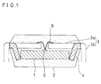
- Figs. 1, 2A and 2B are views showing a semiconductor device in accordance with the first embodiment of the present invention.
- Fig. 1 is a cross-sectional view of the semiconductor device
- Fig. 2A is a plan view of a semiconductor chip and a lead frame of the semiconductor device
- Fig. 2B is a cross-sectional view taken along a line B-B' of Fig. 2A.
- a reference numeral 1 represents a semiconductor chip of rectangular parallelopiped having main and reverse surfaces and side surfaces
- a reference numeral 2 represents a resin package
- a reference numeral 3 represents a connecting lead
- a reference numeral 4 represents a fixing lead
- a reference numeral 5 represents an aluminum electrode provided at a central portion of the semiconductor chip 1
- a reference numeral 6 represents a bonding wire made of Au.
- the lead frame made of 42 alloy or copper, comprises a lead frame main body 15 and a plurality of connecting leads extending inward from the lead frame main body 15, but does not include a die pad.
- An internal lead 3a of the connecting lead 3 extends horizontally in parallel with the upper surface (main surface) of the semiconductor chip 1 until it reaches the inner (or central) region of the semiconductor chip 1, and is electrically connected to the aluminum electrode 5 by means of the bonding wire 6.
- Distal ends 4a of the fixing leads 4 are bent downward toward the semiconductor chip 1, and support the side surfaces of the semiconductor chip 1 by elastic force of the bent portions.
- a reference numeral 16 represents a ground or a common electrode of an electric power source which connects two internal leads 3a, 3a of the connecting leads 3 spaced far from each other and located both ends of and above the semiconductor chip 1.
- a lead frame comprising the lead frame main body 15 (not shown in Fig. 3A), a plurality of connecting leads 3,3, -- extending inward from the lead frame main body 15, and a plurality of fixing leads 4,4,-- having distal ends 4a,4a,-- being bent and extending inward from the lead frame 4.
- a clearance between mutually confronting distal ends 4a, 4a of the fixing leads 4, 4 is slightly smaller than the corresponding size of the semiconductor chip 1.
- the semiconductor chip 1 is then mounted on a jig (not shown).
- the clearance between the mutually confronting distal ends 4a, 4a of the fixing leads 4, 4 is widened using a pin or the like, and the lead frame is set on the jig, thereby assembling the semiconductor chip 1 with the lead frame.
- the internal leads 3a,3a of the connecting leads 3,3 are connected with the aluminum electrode 5 of the semiconductor chip 1 by means of the bonding wire 6, thereby accomplishing electrical connection between the connecting leads 3,3 and the aluminum electrode 5.
- bonding between the connecting leads 3,3 and the aluminum electrode 5 is carried out in a space above the semiconductor chip 1.
- the bonding operation in such a space above the semiconductor chip 1 can be easily carried out by increasing the output of supersonic wave so that a load acting on the internal leads 3a,3a can be decreased as small as possible. If the output of the supersonic wave cannot be increased, it will be preferable to bend the distal end of the internal lead 3a so that the connecting operation can be carried out in a condition where the bent distal end is brought into contact with the semiconductor chip 1.
- the semiconductor chip 1 the internal leads 3a,3a,-- of the connecting leads 3,3,--, the fixing leads 4,4,-- and the bonding wires 6,6-- are sealed or molded together by resin package 2.
- the internal leads 3a,3a,-- of the connecting leads 3,3,-- and the fixing leads 4,4,-- are cut off the lead frame main body 15, and the external leads 3b,3b,-- of the connecting leads 3,3,-- are bent to furnish a semiconductor device of the first embodiment of the present invention.
- the distal ends 4a,4a,-- of the fixing leads 4,4,-- having elasticity and causing an elastic force when deformed with respect to the fixing lead main body are used to support the semiconductor chip 1. Therefore, damage of the semiconductor chip 1 received from the fixing lead 4 is relatively small, and the semiconductor chip 1 is surely held by the lead frame. Furthermore, setting of the semiconductor chip 1 into the lead frame is easy because the setting is carried out under the condition where the clearance of the mutually confronting distal ends 4a,4a of the fixing leads 4,4 is forcibly widened.
- the distal ends 4a,4a of the fixing leads 4,4 are bent and configured in a shape different from the connecting leads 3,3-- having inner internal leads 3a,3a extending straight.
- an arrangement of clamping the semiconductor chip 1 by the distal ends 4a,4a of the fixing leads 4,4 can eliminate the die pad.
- an inside stress of the package 2 can be decreased, thereby increasing the reliability of the package 2.
- Requiring no presence of the die pad brings reduction of thickness in the package 2.
- absence of die bonding paste eliminates the hardening step of the die bonding paste, bringing cost reduction and high reliability.
- Layout of the internal leads 3a,3a,-- of the connecting leads 3,3,-- extending along the upper surface of the semiconductor chip 1 until they reach the internal or central region of the semiconductor chip 1 makes it possible to execute wire bonding operation in the internal or central region of the semiconductor chip 1. It is therefore possible to minimize the thickness of the seal resin between the side edge of the semiconductor chip 1 and the outer surface of the package 2, for example to an extent of approximately 0.5 mm. Furthermore, as the common electrode 16 extends from the internal leads 3a of the connecting leads 3 above the semiconductor chip 1, it becomes possible to dispose the ground or electrodes of the electric power within the internal region of the semiconductor chip 1. Thus, a resistance value is decreased and noise is correspondingly reduced.
- the aluminum electrode 5 can be disposed at the central region of the semiconductor chip 1, the signal transmission path of the semiconductor chip 1 can be reduced to a half of the conventional one.
- high-speed operation and low power consumption are both realized in the semiconductor chip 1.
- Degree of freedom in the design of the semiconductor chip 1 is increased and the width of wiring can be narrowed, reducing the area of the semiconductor chip 1.
- layout of the internal leads 3a,3a,-- extending above the semiconductor chip 1 will be advantageous from the standpoint of effect of heat radiation.
- the pin or the like is used to expand the confronting distal ends 4a, 4a of the fixing leads 4,4 outwardly so as to widen a clearance therebetween and thereafter removes the pin or the like out of the fixing leads 4,4 to allow the elastically deformed portions of the fixing leads 4,4 to spring back to their home positions, thereby setting the semiconductor chip 1 into the lead frame.
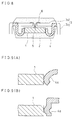
- a bent angle ⁇ formed between the distal end 4a of the fixing lead 4 and the lead frame main body 15 can be a sharp angle as shown in Fig. 4A, or a right angle as shown in Fig. 4B.
- the determination of the bent angle ⁇ will depend on the holding method of the semiconductor chip 1 using the distal ends 4a,4a of the fixing leads 4,4 and the shape of the fixing leads 4,4. However, if the bent angle ⁇ is a dull angle as shown in Fig. 4C, it will be no longer possible to hold the semiconductor chip 1 by the distal ends 4a, 4a of the fixing leads 4,4.
- the method of holding the semiconductor chip 1 using the distal ends 4a,4a of the fixing leads 4,4 can be any of a line contact supporting method shown in Fig. 5A, a surface contact supporting method shown in Fig. 5B, or an edge surface supporting method shown in Fig. 5C.
- the distal end 4a of the fixing lead 4 needs to be cut beforehand into a configuration fitting to the side surface of the semiconductor chip 1.
- the line contact supporting method shown in Fig. 5A will be advantageous in that the semiconductor chip 1 is firmly clamped by a relatively large force, although the damage of the semiconductor chip 1 may be large.
- the surface contact supporting method shown in Figs. 5B and 5C can provide a large contact area which is advantageous to stabilize the support of the semiconductor chip 1 and reduce the damage of the semiconductor chip 1.
- the height of the line contact between the distal end 4a of the fixing lead 4 and the side surface of the semiconductor chip 1 can be a higher point close to the main surface of the semiconductor chip 1 as shown in Fig. 6A, a midpoint of the semiconductor chip 1 as shown in Fig. 6B, or a lower point close to the reverse surface of the semiconductor chip 1 as shown in Fig. 6C.
- the height of the surface contact between the distal end 4a of the fixing lead 4 and the side surface of the semiconductor chip 1 can be a higher region from the main surface of the semiconductor chip 1 to the midpoint as shown in Fig. 6D, a lower region from the midpoint from the reverse surface of the semiconductor chip 1 as shown in Fig.
- the determination of the support position should be optimized by taking account of the configuration of the semiconductor chip 1 or the lead frame, the damage received by the semiconductor chip 1, supporting certainty of the semiconductor chip 1, balance and reliability of the structure of the package 2.
- the distal end 4a of the fixing lead 4 and the semiconductor chip 1 can be variously engaged.
- the semiconductor chip 1 can be sandwiched at the inner surfaces of the distal ends 4a,4a so that the lower edges of the distal ends 4a, 4a extend below the reverse surface of the semiconductor chip 1 as shown in Fig. 7A.
- the semiconductor chip 1 can be engaged with the lower edges of the distal ends 4a, 4a at intermediate portions of the side surfaces of the semiconductor chip 1 so that the lower edges of the distal ends 4a, 4a position higher than the reverse surface of the semiconductor chip 1 as shown in Fig. 7B.
- the semiconductor chip 1 can be engaged with the lower edges of the distal ends 4a,4a at a height close to the reverse surface of the semiconductor chip 1 so that the lowermost edges of the distal ends 4a, 4a just position at the same height as the reverse surface of the semiconductor chip 1.
- the engagement of Fig. 7A is disadvantageous in that the lower edges of the distal ends 4a, 4a protruding lower than the reverse surface of the semiconductor chip 1 possibly collide with the chip stage when the semiconductor chip 1 is set into the lead frame on the chip stage.
- the engagement of Fig. 7B is disadvantageous in that correctly determining the height of the engaging point is difficult, although there is no danger that the distal ends 4a,4a collide with the chip stage.
- the engagement of Fig. 7C is advantageous in that not only there is no danger that the distal edges 4a, 4a collide with the chip stage but positioning of the engaging height is easy.
- a preferable gap between the main surface of the semiconductor chip 1 and the internal lead 3a will be somewhere between 50 to 200 ⁇ m. Because, 50 ⁇ m is a minimum distance required between the internal lead 3a and the main surface of the semiconductor chip 1 for overcoming adverse effect of ⁇ -ray emitted from the internal lead 3a or electric capacity of the internal lead 3a. Meanwhile, 200 ⁇ m is a maximum distance required between the internal lead 3a and the main surface of the semiconductor chip 1 for realizing thickness reduction of the package 2 and utilizing heat radiation effect from the internal leads 3a,3a.
- Fig. 8 is a cross-sectional view showing a semiconductor device in accordance with the second embodiment of the present invention.
- the distal edges 4a, 4a of the fixing leads 4,4 are formed into U shape, thereby causing an elastic force when deformed with respect to the fixing lead main body. With this elastic force, the semiconductor chip 1 can be firmly clamped.
- a clearance between mutually confronting distal ends 4a, 4a of the fixing leads 4, 4 is slightly smaller than the corresponding size of the semiconductor chip 1.
- the semiconductor chip 1 is inserted between the confronting distal edges 4a, 4a of the fixing leads 4, 4 by expanding them outward so as to widen a clearance therebetween by the pushing force of the semiconductor chip 1, thereby setting the semiconductor chip 1 in position in the lead frame.
- the semiconductor chip 1 is firmly clamped by the elastic force of the distal ends 4a, 4a of the fixing leads 4, 4.
- Figs. 9A and 9B are views showing modifications of the second embodiment. Namely, the U-shaped distal ends 4a, 4a of the fixing leads 4, 4 of the second embodiment can be replaced with curved distal ends 4a, 4a shown in Fig. 9A or with partly arc-shaped distal ends 4a, 4a shown in Fig. 9B. These modified distal ends 4a, 4a can bring the same effect as the distal ends 4a, 4a of the second embodiment.
- Figs. 10A and 10B are views showing examples of the distal ends 4a, 4a of the leads 4, 4 in a semiconductor device in accordance with the third embodiment of the present invention.
- the distal ends 4a, 4a of the fixing leads 4, 4 are bent toward the semiconductor chip 1 and then extend straight along the side surfaces of the semiconductor chip 1.
- the distal ends 4a,4a of the fixing leads 4,4 can be bent at a portion confronting the corner of the semiconductor chip 1 so that they then extend along the side surfaces of the semiconductor chip 1 as shown in Fig. 10A, or the distal ends 4a, 4a of the fixing leads 4, 4 can be bent at a portion confronting the side central portion of the semiconductor chip 1 so that they then extend along the side surfaces of the semiconductor chip 1 as shown in Fig. 10B.
- a contact area between the distal ends 4a, 4a of the fixing leads 4,4 and the side surfaces of the semiconductor chip 1 is so increased that a sufficient frictional force can be obtained.
- positional deviation between the distal ends 4a, 4a of the fixing leads 4,4 and the semiconductor chip 1 can be surely prevented and displacement of the semiconductor chip 1 too.
- Fig. 11 is a cross-sectional view showing an arrangement of a semiconductor device in accordance with the fourth embodiment of the present invention.
- a soft metal 7 softer than the semiconductor chip 1 is provided between the distal end 4a of the fixing lead 4 and the side surface of the semiconductor chip 1.
- the soft metal 7 is attached beforehand on the distal end 4a of the fixing lead 4.
- the semiconductor chip 1 is set into the lead frame under the condition where the confronting distal ends 4a, 4a are expanded outward so as to widen a clearance therebetween.
- Adopting such an arrangement makes it possible to reduce the stress that the semiconductor chip 1 receives from the distal ends 4a, 4a of the fixing lead 4, 4 when the semiconductor chip 1 is set in the lead frame and also to reduce the stress that the semiconductor chip 1 receives from the distal ends 4a, 4a of the fixing lead 4, 4 due to heat of resin filled to form the package 2.
- Fig. 12 shows a modification of the fourth embodiment.
- the soft metal 7 is replaced with a resin member 8 having elasticity and insulating ability.
- This modified embodiment can also be effective to reduce the damage of the semiconductor chip 1.
- Fig. 13 is a plan view showing the structure of the lead frame in accordance with a semiconductor device of the fifth embodiment of the present invention.
- a rectangular opening 15a is provided closely to and behind the fixing leads 4 so that a straightly extending narrow portion is provided just behind the fixing leads 4, 4 on the lead frame main body 15.
- the fixing leads 4, 4 are elastically supported with respect to the lead frame main body 15.
- the semiconductor chip 1 is firmly clamped by an elastic force given from the distal ends 4a, 4a of the fixing leads 4, 4.
- a clearance between mutually confronting distal ends 4a, 4a of the fixing leads 4, 4 is slightly smaller than the corresponding size of the semiconductor chip 1.
- the semiconductor chip 1 is set into the lead frame under the condition where the distance of the mutually confronting distal ends 4a, 4a of the fixing leads 4, 4 is expanded slightly larger than the corresponding size of the semiconductor chip 1 by means of a pin or the like. With this arrangement, the semiconductor chip 1 is firmly clamped by the fixing leads 4, 4 which cause an elastic force with respect to the lead frame main body 15.
- Fig. 14 is a cross-sectional view showing an arrangement of a semiconductor device in accordance with the sixth embodiment of the present invention.
- the distal end 4a of the fixing lead 4 is connected to the semiconductor chip 1 via a low melting point metal 9 such as solder.
- Manufacturing method of the semiconductor device in accordance with the sixth embodiment is different from that of the first to fifth embodiments in that a clearance between mutually confronting distal ends 4a, 4a of the fixing leads 4, 4 is set slightly larger than the corresponding size of the semiconductor chip 1, and the low melting point metal 9 is beforehand coated on the inside surfaces of the distal ends 4a, 4a facing to the semiconductor chip 1.
- the semiconductor 1 is set into the lead frame, and subsequently the low melting point metal 9 is melted to connect the distal ends 4a, 4a of the fixing leads 4, 4 with the semiconductor chip 1.
- a preferable melting point of the low melting point metal 9 would be not larger than 400°C in view of the damage received by the semiconductor chip 1.
- Fig. 15 is a first modification of the sixth embodiment, wherein the low melting point metal 9 of the sixth embodiment is replaced with an insulating resin 10 having thermal plasticity, optical hardenability and thermal hardenability.
- the insulating resin 10 having thermal plasticity, optical hardenability and thermal hardenability is coated beforehand on the distal ends 4a, 4a of the fixing leads 4, 4. Under this condition the semiconductor 1 is set into the lead frame, and subsequently heat or light energy is applied to the insulating resin 10, thereby connecting the distal ends 4a, 4a of the fixing leads 4, 4 with the semiconductor chip 1.
- Fig. 16 is a second modification of the sixth embodiment, wherein the low melting point metal 9 of the sixth embodiment is replaced with an insulating film 11 having both surfaces coated with resin having thermal plasticity, optical hardenability and thermal hardenability. Namely, the insulating film 11 has adhesive property. Manufacturing method of the semiconductor device in accordance with the second modification of the sixth embodiment is the same as that of the semiconductor device in accordance with the first modification of the sixth embodiment.
- the low melting point metal 9, the insulating resin 10 or the insulating film 11 is provided beforehand on the distal end 4a of the fixing lead 4 in the above-described sixth embodiment and first and second modifications of the sixth embodiment, it will be possible to insert the low melting point metal 9, the insulating resin 10 or the insulating film 11 between the distal end 4a of the fixing lead 4 and the semiconductor chip 1 when the semiconductor chip 1 is set into the lead frame.
- Figs. 17A to 17C show an example of a manufacturing step of coating the low melting point metal 9 or the insulating resin 10 beforehand on the distal end 4a of the fixing lead 4.
- a lead frame including fixing leads 4, 4 whose distal ends 4a, 4a are bent downward is prepared.
- the distal ends 4a, 4a of the fixing leads 4, 4 are soaked into the low melting point metal 9 or the insulating resin 10 provided on the coating stage 13, thereby attaching a required amount of ball-like low melting point metal 9 or insulating resin 10 on the distal ends 4a,4a of the fixing leads 4,4.
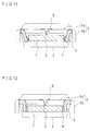
- Figs. 18A, 18B and 19 are views showing a semiconductor device in accordance with the seventh embodiment of the present invention.
- Fig. 18A is a plan view omitting the package 2
- Fig. 18B is a perspective view showing a lead frame
- Fig. 19 is a perspective view omitting the package 2 and the lead frame main body 15.
- the fixing leads 4,4,-- are provided at portions corresponding to the four corners of the semiconductor chip 1.
- the semiconductor chip 1 is supported at its four corners by the distal ends 4a, 4a,-- of the fixing leads 4, 4,--.
- This seventh embodiment is the same as the first to sixth embodiments in that the aluminum electrode 5 is provided at substantially the center of the semiconductor chip 1 and the bonding wire 6 is used to electrically connect the internal lead 3a of the connecting lead 3 and the aluminum electrode 5.
- a distance between diagonally disposed two distal ends 4a, 4a of the fixing leads 4, 4 is slightly smaller than the corresponding diagonal length of the semiconductor chip 1.
- the semiconductor chip 1 is firmly clamped by the distal ends 4a, 4a of the fixing leads 4, 4 which cause an elastic force when deformed with respect to the lead frame main body 15.
- Figs. 20A through 20E are views showing variations of the distal ends 4a, 4a of the fixing leads 4, 4.
- Fig. 20A shows a distal end 4a bent perpendicularly from the fixing lead 4, the distal end 4a further consisting of two bifurcated plates being normal with each other so that the semiconductor chip 1 is brought into contact at its corner with these two bifurcated plates.
- Fig. 20B shows a distal end 4a bent at a dull angle from the fixing lead 4 and having a cutout formed at the lower end thereof.
- Fig. 20C shows an angled distal end 4a bent perpendicularly from the fixing lead 4, the angled distal end 4a being formed into an L shape when seen in the plan view.
- Fig. 20D shows a distal end 4a bent perpendicularly from the fixing lead 4 which in brought into contact with the corner ridge of the semiconductor chip 1.
- Fig. 20E shows bifurcated two distal ends bent from the fixing lead 4 and extending along two surfaces forming a corner of the semiconductor chip 1.
- Configuration of the distal end 4a of the fixing lead 4 should be optimized by taking account of manufacturing cost, supporting strength of the semiconductor chip 1, layout in the design of the lead frame etc.
- the fixing leads 4, 4,-- as having a function of supporting the semiconductor chip 1, it will be preferable that the fixing lead has a function of a ground lead too.
Abstract
Description
- The present invention relates to a semiconductor device having an arrangement of molding a semiconductor chip with resin and a manufacturing method of the same.
- Advances of electronic components in size and thickness reduction technologies in the past few years have made it possible to provide electronic components having highly improved performances, specifically in the field of semiconductor devices such as memories. This tendency will lead to the need of developing semiconductor devices which are compact in size, thin in thickness, low in cost, reliable in performance, and suitable for high-density packaging.
- The package of semiconductor devices, used to be made of ceramic, are being rapidly changed to the resin type to realize the above requirements. Among them, surface mounting type resin molding packages have been increasing their demands since they are advantageous in providing higher mounting density compared with their competitive insertion type packages. The surface mounting type semiconductor packages are generally classified into some specific groups, such as QFP, SOP and SOJ, depending on their detailed constructions.
- A semiconductor device having an SOP-type resin package will be explained hereinafter as a first conventional semiconductor device with reference to Fig. 21.
- Fig. 21 is a cross-sectional view showing the first conventional semiconductor device. In Fig. 21, a
reference numeral 21 represents a semiconductor chip, areference numeral 22 represents a resin package, areference numeral 23 represents a connecting lead made of 42 alloy or copper, areference numeral 25 represents an aluminum electrode, areference numeral 26 represents a bonding wire made of Au, areference numeral 27 represents a die pad, and areference numeral 28 represents a die bonding paste such as Ag paste. - The
semiconductor chip 21 is fixed to the diepad 27 by means of the diebonding paste 28. Aninternal lead 23a of the connectinglead 23 is applied a thin coating of Ag or the like. Thealuminum electrode 25 of thesemiconductor chip 21 is connected to theinternal lead 23a of the connectinglead 23 via thebonding wire 26. The package resin 22 seals thesemiconductor chip 21, thebonding wire 26, thedie pad 27 and theinternal lead 23a therein. Anexternal lead 23b of the connectinglead 23 extends out of thepackage 22. - In the field of general purpose memory devices, an outer configuration of the package, having a small size regulated by the industrial standards such as JEDEC and EIAJ, tends to cause a very severe problem of how such a small package can accommodate a newly developed semiconductor chip having a capacity rapidly expanded every generation.
- Proposed to solve such a problem is an LOC (Lead On Chip) arrangement advantageous to install a large area semiconductor chip into a small-sized package.
- With reference to Fig. 22, a second conventional semiconductor device having an LOC arrangement will be explained.
- Fig. 22 is a cross-sectional view showing the second conventional semiconductor device. In Fig. 22, a
reference numeral 21 represents a semiconductor chip, areference numeral 22 represents a resin package, areference numeral 23 represents a connecting lead, areference numeral 25 represents an aluminum electrode, areference numeral 26 represents a bonding wire, and areference numeral 29 represents a polyimide tape. As shown in Fig. 22, aninternal lead 23a of the connectinglead 23 is disposed above the main surface of thesemiconductor chip 21. - The
polyimide tape 29 has both surfaces on which thermoplastic adhesive material such as polyether amide is coated. Theinternal lead 23a is connected to the main surface of thesemiconductor chip 21 by means of this adhesive material. As thepolyimide tape 29 of the second conventional semiconductor device serves as a means of connecting thesemiconductor chip 21 and the connectinglead 23 in this manner, thedie pad 27 is no longer necessary. - Thus, the semiconductor device having an LOC arrangement allows the
internal lead 23a of the connectinglead 23 to extend above the main surface of thesemiconductor chip 21, so that theinternal lead 23a is connected to thealuminum electrode 25 by means of thebonding wire 26. Accordingly, it becomes possible to reduce the unuseful space around thesemiconductor chip 21, thereby enabling the large-area semiconductor chip 21 to be housed in the small-sizedpackage 22. - However, such a semiconductor device having an LOC arrangement is inherently disadvantageous in that the package has a tall height. For the reduction of the height of the package, Unexamined Japanese Patent Application No. HEI 5-235249/1993 discloses an improved semiconductor device having an arrangement shown in Fig. 23.
- Hereinafter, a third conventional semiconductor device will be explained with reference to Fig. 23. In Fig. 23, a
reference numeral 21 represents a semiconductor chip, areference numeral 22 represents a package, areference numeral 23 represents a connecting lead, areference numeral 25 represents an aluminum electrode, areference numeral 26 represents a bonding wire, and areference numeral 30 represents a bus bar for electric power supply. As shown in Fig. 23, thebus bar 30 extends along the side surface of thesemiconductor chip 21 so that thebus bar 30 is connected through a film with thesemiconductor chip 21. Thus, it becomes possible to omit thedie pad 27 shown in Fig. 21 and thepolyimide 29 shown in Fig. 22. - However, the above-described second conventional semiconductor device has the following problems:
- (1) Presence of the polyimide tape having high hygroscopicity causes moisture absorbed in the polyimide tape to vaporize during solder reflowing operation; therefore, cracks and voids will be easily caused in the semiconductor device.
- (2) Using the polyimide tape having such high hygroscopicity for connecting the internal leads tends to cause leakage between the connecting leads due to hygroscopicity.
- (3) A lead frame with a polyimide tape increases the production cost.
- (4) A process of setting a semiconductor chip into the lead frame requires a thermocompression bonding between the semiconductor chip and the lead frame by means of a 300-400°C high-temperature tool to melt the thermoplastic adhesive material coated on both surfaces of the polyimide tape to connect the semiconductor chip with the internal leads. Therefore, the semiconductor chip is possibly damaged by load and heat of the heating tool.
- The third conventional semiconductor device has the following problems:
- (1) A process of setting the semiconductor chip into a clearance between two bus bars extending in parallel with each other is not easy to carry out.
- (2) Heat of sealing resin acts to thermally expand both the semiconductor chip and the lead frame. Difference of thermal expansion between the semiconductor chip and the lead frame will possibly damage the semiconductor chip by the compression force given from the lead frame.
- (3) Layout of the bus bar extending along the side surface of the semiconductor chip necessarily locates the distal end of the internal lead outside the bus bar; therefore, the LOC arrangement cannot be employed in this third conventional semiconductor device.
- Accordingly, in view of above-described problems encountered in the prior art, a principal object of the present invention is to provide a semiconductor device and its manufacturing method free from the hygroscopicity problem, inexpensive in the production cost, capable of preventing the semiconductor chip from possible damages, facilitating the step of setting the semiconductor chip into the lead frame, and allowing employment of the LOC arrangement, thereby solving above-described problems.
- In order to accomplish this and other related objects, the present invention provides fixing leads having distal ends bent toward the semiconductor, in addition to connecting leads electrically connected to an electrode of a semiconductor chip. With this arrangement, the semiconductor chip is firmly held by the distal ends of the fixing leads.
- A first aspect of the present invention provides a semiconductor device comprising: a semiconductor chip; a plurality of connecting leads which had been extended inward from a lead frame main body, which is separated from the lead frame main body, and which is electrically connected with an electrode of the semiconductor chip; a plurality of fixing leads which had been extended inward from the lead frame main body, which is separated from the lead frame main body, each fixing lead having a distal end bent toward the semiconductor for supporting the semiconductor chip; and a resin package sealing the semiconductor chip, the connecting leads and the fixing leads.
- With this arrangement, the distal ends of the fixing leads cause an elastic force when deformed with respect to the fixing lead main body, so that the semiconductor chip can be supported by this elastic force. Therefore, not only the damage the semiconductor chip receives from the fixing leads is small, but the semiconductor chip is firmly held by the lead frame. Furthermore, as the semiconductor chip can be set in the lead frame under the condition where the distal ends of the fixing leads are expanded outward so as to widen a clearance therebetween, setting of the semiconductor chip is easy.
- As the plural connecting leads and plural fixing leads are provided to extend inward from the lead frame main body, interference between the connecting leads and the fixing leads can be prevented. Thus, it becomes possible to employ the LOC arrangement.
- As the fixing leads have the distal ends being bent, it is easy to discriminate the fixing leads from the connecting leads having internal leads extending straight. Thus, in the image analysis, detection errors are greatly reduced. Electrical connection between the connecting leads and the electrode of the semiconductor chip is surely performed.
- Without using the polyimide tape, the semiconductor chip can be held by the lead frame. Thus, the problem caused by the inherency of polyimide tape can be eliminated.
- It will be preferable to adopt an LOC arrangement wherein the connecting leads have internal leads extending above and along a main surface of the semiconductor chip and electrically connected to the electrode of the semiconductor chip.
- With this arrangement, it is not necessary to provide the bonding wire at the side of the semiconductor chip. Therefore, the thickness of a seal resin between the side edge of the semiconductor chip and the outer surface of the package can be minimized, resulting in size reduction of the package. As a common electrode is extendable from the internal leads of the connecting leads on the semiconductor chip, not only dispersion layout of the common electrode is realized but the electrode can be disposed within the internal region of the semiconductor chip. Accordingly, a resistance component is reduced and noise is reduced. Thus, the signal transmission path in the semiconductor chip can be shortened, realizing high speed operation and low power consumption.
- The distal end of the fixing lead can support a side surface of the semiconductor chip. Thus, support of the semiconductor chip by the distal ends is ensured. Mistake is reduced in the setting of the semiconductor chip into the lead frame.
- In this case, it is preferable that the distal end of the fixing lead has a surface brought into contact with the side surface of the semiconductor chip. With this arrangement, a contact area between the distal end of the fixing lead and the side surface of the semiconductor chip is enlarged. Therefore, support of the semiconductor chip by the distal ends of the fixing leads can be further ensured. Mistake is further reduced in the setting of the semiconductor chip into the lead frame.
- When the distal ends of the fixing leads are arranged to support the corners of the semiconductor chip, interference between the fixing leads and the connecting leads can be avoided, increasing the degree of freedom in designing the lead frame.
- It will be preferable that soft metal or an elastic member is interposed between the distal end of the fixing lead and the side surface of the semiconductor chip, because a mechanical stress the semiconductor chip receives from the distal ends of the fixing leads can be reduced. Thus, the damage the semiconductor chip receives from the fixing leads can be reduced.
- The distal end of the fixing lead may be connected with the side surface of the semiconductor chip by resin or low melting point metal. With adoption of such resin or low melting point metal, the semiconductor chip can be installed into the lead frame under the condition where the distal ends of the fixing leads are spaced from the side surfaces of the semiconductor chip. Hence, the damage the semiconductor receives from the fixing leads can be reduced in the step of setting the semiconductor chip into the lead frame.
- Furthermore, the distal end of the fixing lead may be connected with the side surface of the semiconductor chip by adhesive insulating film. In this case, not only connecting the distal ends of the fixing leads with the semiconductor chip is easy but insulating property between the fixing leads and the semiconductor chip is sufficiently increased.
- The fixing lead may serve as a ground lead, since a ground lead can be brought into contact with the side surface of the semiconductor chip whose electrical potential should be grounded. Thus, it is unnecessary to prepare a ground lead independently.
- The distal end of the fixing lead may be an angled plate formed into an L shape when seen in the plan view, so that the angled plate can support the corner of the semiconductor chip. With this arrangement, support of the semiconductor chip by the distal ends of the fixing leads can be stabilized.
- A second aspect of the present invention provides a manufacturing method of a semiconductor device comprising: a first step of providing a lead frame main body, a plurality of connecting leads extending inward from the lead frame main body for providing electrical connection, and a plurality of fixing leads extending inward from the lead frame main body and having distal ends bent toward the semiconductor; a second step of holding the semiconductor chip by the distal ends of the fixing leads; a third step of sealing the semiconductor chip, the connecting leads and the fixing leads with resin to form a resin package; and a fourth step of cutting the connecting leads and fixing leads from the lead frame main body. With this manufacturing method, the semiconductor device of the first aspect of the present invention previously explained can be easily manufactured.
- This manufacturing method may further comprise a step of electrically connecting an electrode of the semiconductor chip with internal leads of the connecting leads by means of a bonding wire, so that the step is executed between the second and third steps.
- The first step may comprise a step of setting a clearance between distal ends of confronting fixing leads to be slightly smaller than a corresponding size of the semiconductor chip, and the second step may comprise a distal ends expanding step of expanding the distal ends of the confronting fixing leads outward so that the clearance between the distal ends of the confronting fixing leads becomes slightly larger than the corresponding size of the semiconductor chip, a semiconductor chip setting step of placing the semiconductor chip into an enlarged space formed between the distal ends, and a semiconductor chip holding step of clamping the semiconductor chip by the distal ends of the confronting fixing leads which are sprung back inward.
- With these steps, the semiconductor chip can be installed into the lead frame under the condition where the clearance between the distal ends of the fixing leads is widened larger than the corresponding size of the semiconductor chip. Hence, the damage the semiconductor chip receives from the fixing leads can be reduced.
- In this case, the first step may comprise a step of providing each fixing lead so as to cause an elastic force when deformed with respect to the lead frame main body, and the semiconductor chip holding step in the second step may comprise a step of clamping the semiconductor chip by the elastic force of the fixing lead deformed with respect to the lead frame.
- With these steps, plural fixing leads cause an elastic force when deformed with respect to the lead frame main body, thereby making it possible to clamp the semiconductor chip firmly by the distal ends of the fixing leads. Not only the damage the semiconductor chip receives from the fixing leads is further decreased but the semiconductor chip is further firmly held by the lead frame. The setting step of placing the semiconductor chip between the widened distal ends of the fixing leads is easily carried out.
- The first step may comprise a step of providing the distal ends of the fixing leads so as to cause an elastic force when deformed with respect to the fixing lead main body, and the semiconductor chip holding step in the second step may comprise a step of clamping the semiconductor chip by the elastic force of the distal ends of the fixing leads deformed with respect to the lead frame.
- With these steps, distal end of plural fixing leads cause an elastic force when deformed with respect to the lead frame main body, thereby making it possible to clamp the semiconductor chip firmly by the distal ends of the fixing leads. Not only the damage the semiconductor chip receives from the fixing leads is further decreased but the semiconductor chip is further firmly held by the lead frame. The setting step of placing the semiconductor chip between the widened distal ends of the fixing leads is easily carried out.
- The distal ends expanding step in the second step comprises a step of heating the lead frame so that the distal ends of the fixing leads expand outward.
- With this step, the distal ends of the fixing leads can be expanded outward so as to widen a clearance therebetween without causing mechanical deformation. Thus, smooth execution is assured in both the distal ends expanding step and the semiconductor chip holding step in the second step.
- The semiconductor chip holding step in the second step may comprise a step of providing a soft member softer than the semiconductor chip intervening between the distal ends of the confronting fixing leads and the semiconductor chip, so as to clamp the semiconductor chip between the distal ends of the confronting fixing leads via the soft member.
- With this step, the damage the semiconductor chip received from the fixing leads is further reduced. If the soft member is an elastic member, the damage the semiconductor chip received from the fixing leads is yet further reduced.
- The first step may comprise a step of setting a clearance between distal ends of confronting fixing leads to be slightly larger than a corresponding size of the semiconductor chip, and the second step may comprise a semiconductor chip setting step of placing the semiconductor chip into a space formed between the distal ends, and a semiconductor chip holding step of connecting the distal ends of the confronting fixing leads with the semiconductor chip, thereby holding the semiconductor chip between the distal ends of the confronting fixing leads.
- By doing this, the semiconductor chip can be installed into the lead frame under the condition where a sufficient clearance is provided between the semiconductor chip and the distal ends of the fixing leads. Thus, the damage the semiconductor receives from the fixing leads is reduced in the semiconductor chip setting step.
- The semiconductor chip holding step in the second step may comprise a step of connecting the distal ends of the confronting fixing leads with the semiconductor chip by low melting point metal. By doing this, thermal damage given to the semiconductor chip is reduced. Hence, the distal ends of the fixing leads can be surely connected with the semiconductor chip.
- The semiconductor chip holding step in the second step may comprise a step of connecting the distal ends of the confronting fixing leads with the semiconductor chip by adhesive insulating resin. By doing this, thermal damage given to the semiconductor chip is completely eliminated. Hence, not only the distal ends of the fixing leads can be surely connected with the semiconductor chip but insulating property between the fixing leads and the semiconductor chip is increased.
- The semiconductor chip holding step in the second step may comprise a step of connecting the distal ends of the confronting fixing leads with the semiconductor chip via insulating film having adhesive property. By doing this, not only connection between the distal ends of the fixing leads and the low melting point metal is facilitated but insulating property between the fixing leads and the semiconductor chip is increased.
- The second step may comprise a step of holding a side surface of the semiconductor chip by a distal end of the fixing lead. By doing this, the semiconductor chip is surely held.
- The second step may comprise a step of holding side surfaces forming a corner of the semiconductor chip by the distal ends of the fixing leads. By doing this, it becomes possible to avoid an interference between the fixing leads and the connecting leads, assuring the degree of freedom in the design of the lead frame.
- The above and other objects, features and advantages of the present invention will become more apparent from the following detailed description which is to be read in conjunction with the accompanying drawings, in which:
- Fig. 1 is a cross-sectional view showing a semiconductor device in accordance with a first embodiment of the present invention;
- Fig. 2A is a plan view showing the semiconductor device in accordance with the first embodiment of the present invention, and Fig. 2B is a cross-sectional view taken along a line B-B' of Fig. 2A;
- Figs. 3A-3E are cross-sectional views showing manufacturing steps of the semiconductor device in accordance with the first embodiment of the present invention;
- Figs. 4A-4C are cross-sectional views respectively illustrating an angular relation of the distal end of the fixing lead to the lead frame in accordance with the first embodiment of the present invention;
- Figs. 5A-5C are cross-sectional views respectively illustrating a method of supporting a semiconductor chip between distal ends of the fixing leads in accordance with the first embodiment of the present invention;
- Figs. 6A-6F are cross-sectional views respectively illustrating an altitudinal relation between the distal ends of the fixing leads and the semiconductor chip sandwiched therebetween in accordance with the first embodiment of the present invention;
- Figs. 7A-7C are cross-sectional views respectively illustrating a positional relation between the lowermost distal ends of the fixing leads and the reverse surface of the semiconductor chip in accordance with the first embodiment of the present invention;
- Fig. 8 is a cross-sectional view showing a semiconductor device in accordance with a second embodiment of the present invention;
- Figs. 9A and 9B are cross-sectional views respectively showing configuration of the distal end of the fixing lead in accordance with a modified embodiment of the second embodiment in accordance with the present invention;
- Figs. 10A and 10B are perspective views respectively showing distal ends of the fixing leads of a semiconductor device in accordance with a third embodiment of the present invention;
- Fig. 11 is a cross-sectional view showing a semiconductor device in accordance with a fourth embodiment of the present invention;
- Fig. 12 is a cross-sectional view showing a semiconductor device in accordance with a modified embodiment of the fourth embodiment of the present invention;
- Fig. 13 is a plan view showing a lead frame of a semiconductor device in accordance with a fifth embodiment of the present invention;
- Fig. 14 is a cross-sectional view showing a semiconductor device in accordance with a sixth embodiment of the present invention;
- Fig. 15 is a cross-sectional view showing a semiconductor device in accordance with a first modified embodiment of the sixth embodiment of the present invention;
- Fig. 16 is a cross-sectional view showing a semiconductor device in accordance with a second modified embodiment of the sixth embodiment of the present invention;
- Figs. 17A-17C are cross-sectional views illustrating a step of coating low-melting point metal or insulating resin on the distal end of the fixing lead in the manufacturing method of the semiconductor device in accordance with the sixth embodiment or the first modified embodiment of the sixth embodiment of the present invention;
- Fig. 18A is a plan view showing a semiconductor device in accordance with a seventh embodiment of the present invention, omitting a package thereof, and Fig. 18B is a perspective view showing a lead frame of the seventh embodiment;
- Fig. 19 is a perspective view showing the semiconductor device in accordance with the seventh embodiment of the present invention, omitting the package and the lead frame;
- Figs. 20A-20E are views respectively showing configuration of the distal end of a fixing lead of the semiconductor device in accordance with the seventh embodiment of the present invention;
- Fig. 21 is a cross-sectional view showing the first conventional semiconductor device;
- Fig. 22 is a cross-sectional view showing the second conventional semiconductor device; and
- Fig. 23 is a cross-sectional view showing the third conventional semiconductor device.
- Hereinafter, preferred embodiments of the present invention will be explained in greater detail with reference to the accompanying drawings.
- Figs. 1, 2A and 2B are views showing a semiconductor device in accordance with the first embodiment of the present invention. Fig. 1 is a cross-sectional view of the semiconductor device, Fig. 2A is a plan view of a semiconductor chip and a lead frame of the semiconductor device, and Fig. 2B is a cross-sectional view taken along a line B-B' of Fig. 2A.
- In the drawings, a
reference numeral 1 represents a semiconductor chip of rectangular parallelopiped having main and reverse surfaces and side surfaces, areference numeral 2 represents a resin package, areference numeral 3 represents a connecting lead, areference numeral 4 represents a fixing lead, areference numeral 5 represents an aluminum electrode provided at a central portion of thesemiconductor chip 1, areference numeral 6 represents a bonding wire made of Au. The lead frame, made of 42 alloy or copper, comprises a lead framemain body 15 and a plurality of connecting leads extending inward from the lead framemain body 15, but does not include a die pad. Aninternal lead 3a of the connectinglead 3 extends horizontally in parallel with the upper surface (main surface) of thesemiconductor chip 1 until it reaches the inner (or central) region of thesemiconductor chip 1, and is electrically connected to thealuminum electrode 5 by means of thebonding wire 6. - Distal ends 4a of the fixing leads 4 are bent downward toward the
semiconductor chip 1, and support the side surfaces of thesemiconductor chip 1 by elastic force of the bent portions. - Above-described
semiconductor chip 1, the connectinglead 3, the fixinglead 4 and thebonding wire 6 are hermetically sealed or molded together into apackage 2. Anexternal lead 3b of the connectinglead 3 is positioned out of thepackage 2 and is formed into a predetermined shape. In Fig. 2A, areference numeral 16 represents a ground or a common electrode of an electric power source which connects twointernal leads semiconductor chip 1. - Hereinafter, a manufacturing method of the semiconductor device in accordance with the first embodiment will be explained with reference to Figs. 3A to 3E.
- As illustrated in Fig. 3A, there is provided a lead frame comprising the lead frame main body 15 (not shown in Fig. 3A), a plurality of connecting
leads main body 15, and a plurality of fixing leads 4,4,-- havingdistal ends lead frame 4. A clearance between mutually confrontingdistal ends semiconductor chip 1. Thesemiconductor chip 1 is then mounted on a jig (not shown). The clearance between the mutually confrontingdistal ends semiconductor chip 1 with the lead frame. - Subsequently, above-described pin or the like is removed so that the
distal ends distal ends semiconductor chip 1 from both sides thereof, thereby completely clamping thesemiconductor chip 1 by the lead frame. - Next, as illustrated in Fig. 3C, the
internal leads aluminum electrode 5 of thesemiconductor chip 1 by means of thebonding wire 6, thereby accomplishing electrical connection between the connecting leads 3,3 and thealuminum electrode 5. In this first embodiment of the present invention, bonding between the connecting leads 3,3 and thealuminum electrode 5 is carried out in a space above thesemiconductor chip 1. The bonding operation in such a space above thesemiconductor chip 1 can be easily carried out by increasing the output of supersonic wave so that a load acting on theinternal leads internal lead 3a so that the connecting operation can be carried out in a condition where the bent distal end is brought into contact with thesemiconductor chip 1. - Next, as illustrated in Fig. 3D, the
semiconductor chip 1, theinternal leads bonding wires resin package 2. - Thereafter, as illustrated in Fig. 3E, the
internal leads main body 15, and theexternal leads - According to the semiconductor device of the first embodiment, the
distal ends semiconductor chip 1. Therefore, damage of thesemiconductor chip 1 received from the fixinglead 4 is relatively small, and thesemiconductor chip 1 is surely held by the lead frame. Furthermore, setting of thesemiconductor chip 1 into the lead frame is easy because the setting is carried out under the condition where the clearance of the mutually confrontingdistal ends - Furthermore, from the view point of reducing detection errors in the image analysis in a step of connecting the connecting leads 3,3 with the
aluminum electrode 5 by means of thebonding wires distal ends internal leads - Moreover, an arrangement of clamping the
semiconductor chip 1 by thedistal ends package 2 can be prevented from occurring at the reverse surface of the die pad but an inside stress of thepackage 2 can be decreased, thereby increasing the reliability of thepackage 2. Requiring no presence of the die pad brings reduction of thickness in thepackage 2. Furthermore, absence of die bonding paste eliminates the hardening step of the die bonding paste, bringing cost reduction and high reliability. - Layout of the
internal leads semiconductor chip 1 until they reach the internal or central region of thesemiconductor chip 1 makes it possible to execute wire bonding operation in the internal or central region of thesemiconductor chip 1. It is therefore possible to minimize the thickness of the seal resin between the side edge of thesemiconductor chip 1 and the outer surface of thepackage 2, for example to an extent of approximately 0.5 mm. Furthermore, as thecommon electrode 16 extends from theinternal leads 3a of the connecting leads 3 above thesemiconductor chip 1, it becomes possible to dispose the ground or electrodes of the electric power within the internal region of thesemiconductor chip 1. Thus, a resistance value is decreased and noise is correspondingly reduced. Still further, as thealuminum electrode 5 can be disposed at the central region of thesemiconductor chip 1, the signal transmission path of thesemiconductor chip 1 can be reduced to a half of the conventional one. Thus, high-speed operation and low power consumption are both realized in thesemiconductor chip 1. Degree of freedom in the design of thesemiconductor chip 1 is increased and the width of wiring can be narrowed, reducing the area of thesemiconductor chip 1. Furthermore, layout of theinternal leads semiconductor chip 1 will be advantageous from the standpoint of effect of heat radiation. - According to the above-described first embodiment, the pin or the like is used to expand the confronting
distal ends semiconductor chip 1 into the lead frame. Alternatively, it is possible to heat the lead frame so as to allow thedistal ends semiconductor chip 1 therebetween and then to cool down the lead frame to allow thedistal ends semiconductor chip 1. - A bent angle ϑ formed between the
distal end 4a of the fixinglead 4 and the lead framemain body 15 can be a sharp angle as shown in Fig. 4A, or a right angle as shown in Fig. 4B. The determination of the bent angle ϑ will depend on the holding method of thesemiconductor chip 1 using the distal ends 4a,4a of the fixing leads 4,4 and the shape of the fixing leads 4,4. However, if the bent angle ϑ is a dull angle as shown in Fig. 4C, it will be no longer possible to hold thesemiconductor chip 1 by thedistal ends - The method of holding the
semiconductor chip 1 using the distal ends 4a,4a of the fixing leads 4,4 can be any of a line contact supporting method shown in Fig. 5A, a surface contact supporting method shown in Fig. 5B, or an edge surface supporting method shown in Fig. 5C. In the case of the edge surface supporting method shown in Fig. 5C, thedistal end 4a of the fixinglead 4 needs to be cut beforehand into a configuration fitting to the side surface of thesemiconductor chip 1. The line contact supporting method shown in Fig. 5A will be advantageous in that thesemiconductor chip 1 is firmly clamped by a relatively large force, although the damage of thesemiconductor chip 1 may be large. The surface contact supporting method shown in Figs. 5B and 5C can provide a large contact area which is advantageous to stabilize the support of thesemiconductor chip 1 and reduce the damage of thesemiconductor chip 1. - Regarding the height of the line contact between the
distal end 4a of the fixinglead 4 and the side surface of thesemiconductor chip 1 can be a higher point close to the main surface of thesemiconductor chip 1 as shown in Fig. 6A, a midpoint of thesemiconductor chip 1 as shown in Fig. 6B, or a lower point close to the reverse surface of thesemiconductor chip 1 as shown in Fig. 6C. The height of the surface contact between thedistal end 4a of the fixinglead 4 and the side surface of thesemiconductor chip 1 can be a higher region from the main surface of thesemiconductor chip 1 to the midpoint as shown in Fig. 6D, a lower region from the midpoint from the reverse surface of thesemiconductor chip 1 as shown in Fig. 6E, or a whole region ranging from the main surface to the reverse surface of thesemiconductor chip 1 as shown in Fig. 6F. The determination of the support position should be optimized by taking account of the configuration of thesemiconductor chip 1 or the lead frame, the damage received by thesemiconductor chip 1, supporting certainty of thesemiconductor chip 1, balance and reliability of the structure of thepackage 2. - The
distal end 4a of the fixinglead 4 and thesemiconductor chip 1 can be variously engaged. For example, thesemiconductor chip 1 can be sandwiched at the inner surfaces of thedistal ends distal ends semiconductor chip 1 as shown in Fig. 7A. Alternatively, thesemiconductor chip 1 can be engaged with the lower edges of thedistal ends semiconductor chip 1 so that the lower edges of thedistal ends semiconductor chip 1 as shown in Fig. 7B. Furthermore, thesemiconductor chip 1 can be engaged with the lower edges of thedistal ends semiconductor chip 1 so that the lowermost edges of thedistal ends semiconductor chip 1. - However, the engagement of Fig. 7A is disadvantageous in that the lower edges of the
distal ends semiconductor chip 1 possibly collide with the chip stage when thesemiconductor chip 1 is set into the lead frame on the chip stage. The engagement of Fig. 7B is disadvantageous in that correctly determining the height of the engaging point is difficult, although there is no danger that thedistal ends distal edges - A preferable gap between the main surface of the
semiconductor chip 1 and theinternal lead 3a will be somewhere between 50 to 200µm. Because, 50µm is a minimum distance required between theinternal lead 3a and the main surface of thesemiconductor chip 1 for overcoming adverse effect of α-ray emitted from theinternal lead 3a or electric capacity of theinternal lead 3a. Meanwhile, 200µm is a maximum distance required between theinternal lead 3a and the main surface of thesemiconductor chip 1 for realizing thickness reduction of thepackage 2 and utilizing heat radiation effect from theinternal leads - Fig. 8 is a cross-sectional view showing a semiconductor device in accordance with the second embodiment of the present invention. In this second embodiment, the
distal edges semiconductor chip 1 can be firmly clamped. In the same manner as in the first embodiment, a clearance between mutually confrontingdistal ends semiconductor chip 1. Thesemiconductor chip 1 is inserted between the confrontingdistal edges semiconductor chip 1, thereby setting thesemiconductor chip 1 in position in the lead frame. Thus, thesemiconductor chip 1 is firmly clamped by the elastic force of thedistal ends - Figs. 9A and 9B are views showing modifications of the second embodiment. Namely, the U-shaped
distal ends distal ends distal ends distal ends - Figs. 10A and 10B are views showing examples of the
distal ends leads distal ends semiconductor chip 1 and then extend straight along the side surfaces of thesemiconductor chip 1. In this case, thedistal ends semiconductor chip 1 so that they then extend along the side surfaces of thesemiconductor chip 1 as shown in Fig. 10A, or thedistal ends semiconductor chip 1 so that they then extend along the side surfaces of thesemiconductor chip 1 as shown in Fig. 10B. - By employing such an arrangement, a contact area between the
distal ends semiconductor chip 1 is so increased that a sufficient frictional force can be obtained. Thus, positional deviation between thedistal ends semiconductor chip 1 can be surely prevented and displacement of thesemiconductor chip 1 too. - Fig. 11 is a cross-sectional view showing an arrangement of a semiconductor device in accordance with the fourth embodiment of the present invention. In this fourth embodiment, a
soft metal 7 softer than thesemiconductor chip 1 is provided between thedistal end 4a of the fixinglead 4 and the side surface of thesemiconductor chip 1. To manufacture the semiconductor device in accordance with the third embodiment, thesoft metal 7 is attached beforehand on thedistal end 4a of the fixinglead 4. Then, in the same manner as the first embodiment, thesemiconductor chip 1 is set into the lead frame under the condition where the confrontingdistal ends - Adopting such an arrangement makes it possible to reduce the stress that the
semiconductor chip 1 receives from thedistal ends lead semiconductor chip 1 is set in the lead frame and also to reduce the stress that thesemiconductor chip 1 receives from thedistal ends lead package 2. - Fig. 12 shows a modification of the fourth embodiment. In this modification, the
soft metal 7 is replaced with aresin member 8 having elasticity and insulating ability. This modified embodiment can also be effective to reduce the damage of thesemiconductor chip 1. - Fig. 13 is a plan view showing the structure of the lead frame in accordance with a semiconductor device of the fifth embodiment of the present invention. In this fifth embodiment, a rectangular opening 15a is provided closely to and behind the fixing leads 4 so that a straightly extending narrow portion is provided just behind the fixing leads 4, 4 on the lead frame
main body 15. Thus, the fixing leads 4, 4 are elastically supported with respect to the lead framemain body 15. In other words, thesemiconductor chip 1 is firmly clamped by an elastic force given from thedistal ends distal ends semiconductor chip 1. Thesemiconductor chip 1 is set into the lead frame under the condition where the distance of the mutually confrontingdistal ends semiconductor chip 1 by means of a pin or the like. With this arrangement, thesemiconductor chip 1 is firmly clamped by the fixing leads 4, 4 which cause an elastic force with respect to the lead framemain body 15. - Fig. 14 is a cross-sectional view showing an arrangement of a semiconductor device in accordance with the sixth embodiment of the present invention. In this sixth embodiment, the
distal end 4a of the fixinglead 4 is connected to thesemiconductor chip 1 via a lowmelting point metal 9 such as solder. Manufacturing method of the semiconductor device in accordance with the sixth embodiment is different from that of the first to fifth embodiments in that a clearance between mutually confrontingdistal ends semiconductor chip 1, and the lowmelting point metal 9 is beforehand coated on the inside surfaces of thedistal ends semiconductor chip 1. Under this condition thesemiconductor 1 is set into the lead frame, and subsequently the lowmelting point metal 9 is melted to connect thedistal ends semiconductor chip 1. A preferable melting point of the lowmelting point metal 9 would be not larger than 400°C in view of the damage received by thesemiconductor chip 1. - Fig. 15 is a first modification of the sixth embodiment, wherein the low
melting point metal 9 of the sixth embodiment is replaced with an insulatingresin 10 having thermal plasticity, optical hardenability and thermal hardenability. To manufacture the semiconductor device in accordance with the first modification of the sixth embodiment, the insulatingresin 10 having thermal plasticity, optical hardenability and thermal hardenability is coated beforehand on thedistal ends semiconductor 1 is set into the lead frame, and subsequently heat or light energy is applied to the insulatingresin 10, thereby connecting thedistal ends semiconductor chip 1. - Fig. 16 is a second modification of the sixth embodiment, wherein the low
melting point metal 9 of the sixth embodiment is replaced with an insulatingfilm 11 having both surfaces coated with resin having thermal plasticity, optical hardenability and thermal hardenability. Namely, the insulatingfilm 11 has adhesive property. Manufacturing method of the semiconductor device in accordance with the second modification of the sixth embodiment is the same as that of the semiconductor device in accordance with the first modification of the sixth embodiment. - In the arrangements of the sixth embodiment, and first and second modifications of the sixth embodiment wherein the clearance between the mutually confronting
distal ends semiconductor chip 1, it will be possible to connect only one side surface of thesemiconductor chip 1 with thedistal end 4a of the fixinglead 4. - Although the low
melting point metal 9, the insulatingresin 10 or the insulatingfilm 11 is provided beforehand on thedistal end 4a of the fixinglead 4 in the above-described sixth embodiment and first and second modifications of the sixth embodiment, it will be possible to insert the lowmelting point metal 9, the insulatingresin 10 or the insulatingfilm 11 between thedistal end 4a of the fixinglead 4 and thesemiconductor chip 1 when thesemiconductor chip 1 is set into the lead frame. - Figs. 17A to 17C show an example of a manufacturing step of coating the low
melting point metal 9 or the insulatingresin 10 beforehand on thedistal end 4a of the fixinglead 4. Namely, as illustrated in Fig. 17A, a lead frame including fixing leads 4, 4 whosedistal ends distal ends melting point metal 9 or the insulatingresin 10 provided on thecoating stage 13, thereby attaching a required amount of ball-like lowmelting point metal 9 or insulatingresin 10 on thedistal ends - Figs. 18A, 18B and 19 are views showing a semiconductor device in accordance with the seventh embodiment of the present invention. Fig. 18A is a plan view omitting the
package 2, Fig. 18B is a perspective view showing a lead frame, and Fig. 19 is a perspective view omitting thepackage 2 and the lead framemain body 15. - In the seventh embodiment, the fixing leads 4,4,-- are provided at portions corresponding to the four corners of the
semiconductor chip 1. Thus, thesemiconductor chip 1 is supported at its four corners by thedistal ends aluminum electrode 5 is provided at substantially the center of thesemiconductor chip 1 and thebonding wire 6 is used to electrically connect theinternal lead 3a of the connectinglead 3 and thealuminum electrode 5. - In the seventh embodiment, a distance between diagonally disposed two
distal ends semiconductor chip 1. Thesemiconductor chip 1 set into the lead frame under the condition where thedistal ends semiconductor chip 1 is firmly clamped by thedistal ends main body 15. - Figs. 20A through 20E are views showing variations of the
distal ends distal end 4a bent perpendicularly from the fixinglead 4, thedistal end 4a further consisting of two bifurcated plates being normal with each other so that thesemiconductor chip 1 is brought into contact at its corner with these two bifurcated plates. Fig. 20B shows adistal end 4a bent at a dull angle from the fixinglead 4 and having a cutout formed at the lower end thereof. Fig. 20C shows an angleddistal end 4a bent perpendicularly from the fixinglead 4, the angleddistal end 4a being formed into an L shape when seen in the plan view. Thus, thesemiconductor chip 1 is brought into contact at its corner with the two surfaces of the angleddistal end 4a. Fig. 20D shows adistal end 4a bent perpendicularly from the fixinglead 4 which in brought into contact with the corner ridge of thesemiconductor chip 1. Fig. 20E shows bifurcated two distal ends bent from the fixinglead 4 and extending along two surfaces forming a corner of thesemiconductor chip 1. Thus, thesemiconductor chip 1 is brought into contact at its corner with the surfaces of the bifurcated two distal ends. Configuration of thedistal end 4a of the fixinglead 4 should be optimized by taking account of manufacturing cost, supporting strength of thesemiconductor chip 1, layout in the design of the lead frame etc. - Although the above-explained embodiments show the fixing leads 4, 4,-- as having a function of supporting the
semiconductor chip 1, it will be preferable that the fixing lead has a function of a ground lead too. - Although the above-described embodiments show the
bonding wire 6 connecting theinternal lead 3a of the connectinglead 3 with thealuminum electrode 5 of thesemiconductor chip 1, it will be possible to replace thebonding wire 6 with a solder or aluminum bump to directly connect the electrodes, or anisotropic conductive resin or the like. - Furthermore, although the above-described embodiments employ the LOC arrangement which allows the
internal leads semiconductor chip 1, it is needless to say that an ordinary arrangement which necessitates theinternal leads semiconductor chip 1. - As this invention may be embodied in several forms without departing from the spirit of essential characteristics thereof, the present embodiments as described are therefore intended to be only illustrative and not restrictive, since the scope of the invention is defined by the appended claims rather than by the description preceding them, and all changes that fall within the metes and bounds of the claims, or equivalents of such metes and bounds, are therefore intended to be embraced by the claims.
Claims (27)
- A semiconductor device comprising:
a semiconductor chip;
a plurality of connecting leads which had been extended inward from a lead frame main body, which is separated from said lead frame main body, and which is electrically connected with an electrode of said semiconductor chip;
a plurality of fixing leads which had been extended inward from the lead frame main body, which is separated from said lead frame main body, each fixing lead having a distal end bent toward the semiconductor for supporting said semiconductor chip; and
a resin package sealing said semiconductor chip, said connecting leads and said fixing leads. - The semiconductor device in accordance with claim 1, wherein said connecting leads have internal leads extending above and along a main surface of said semiconductor chip and electrically connected to said electrode of the semiconductor chip.
- The semiconductor device in accordance with claim 1, wherein said distal end of the fixing lead supports a side surface of said semiconductor chip.
- The semiconductor device in accordance with claim 3, wherein said distal end of the fixing lead has a surface brought into contact with the side surface of said semiconductor chip.
- The semiconductor device in accordance with claim 3, wherein soft metal or an elastic member is interposed between said distal end of the fixing lead and the side surface of said semiconductor chip.
- The semiconductor device in accordance with claim 3, wherein said distal end of the fixing lead is connected with the side surface of said semiconductor chip by resin or low melting point metal.
- The semiconductor device in accordance with claim 3, wherein said distal end of the fixing lead is connected with the side surface of said semiconductor chip by adhesive insulating film.
- The semiconductor device in accordance with claim 3, wherein said fixing lead serves as a ground lead.
- The semiconductor device in accordance with claim 1, wherein said distal end of the fixing lead supports a corner of said semiconductor chip.
- The semiconductor device in accordance with claim 9, wherein said distal end of the fixing lead is an angled plate formed into an L shape when seen in the plan view, said angled plate supporting the corner of the semiconductor chip.
- The semiconductor device in accordance with claim 9, wherein soft metal or an elastic member is interposed between the distal end of the fixing lead and the corner of the semiconductor chip.
- The semiconductor device in accordance with claim 9, wherein said distal end of the fixing lead is connected with the corner of said semiconductor chip by resin or low melting point metal.
- The semiconductor device in accordance with claim 9, wherein said fixing lead serves as a ground lead.
- A manufacturing method of a semiconductor device comprising:
a first step of providing a lead frame main body, a plurality of connecting leads extending inward from said lead frame main body for providing electrical connection, and a plurality of fixing leads extending inward from the lead frame main body and having distal ends bent toward the semiconductor;
a second step of holding said semiconductor chip by said distal ends of the fixing leads;
a third step of sealing said semiconductor chip, said connecting leads and said fixing leads with resin to form a resin package; and
a fourth step of cutting said connecting leads and fixing leads off said lead frame main body. - the manufacturing method of a semiconductor device in accordance with claim 14, further comprising a step of electrically connecting an electrode of said semiconductor chip with internal leads of said connecting leads by means of a bonding wire, said step being executed between said second and third steps.
- The manufacturing method of a semiconductor device in accordance with claim 14, wherein
said first step comprises a step of setting a clearance between distal ends of confronting fixing leads to be slightly smaller than a corresponding size of the semiconductor chip, and
said second step comprises a distal ends expanding step of expanding said distal ends of the confronting fixing leads outward so that the clearance between said distal ends of the confronting fixing leads becomes slightly larger than the corresponding size of the semiconductor chip, a semiconductor chip setting step of placing said semiconductor chip into an enlarged space formed between said distal ends, and a semiconductor chip holding step of clamping said semiconductor chip by said distal ends of the confronting fixing leads which are sprung back inward. - The manufacturing method of a semiconductor device in accordance with claim 16, wherein
said first step comprises a step of providing said fixing lead so as to cause an elastic force when deformed with respect to the lead frame main body, and
said semiconductor chip holding step in said second step comprises a step of clamping said semiconductor chip by the elastic force of the fixing leads deformed with respect to said lead frame. - The manufacturing method of a semiconductor device in accordance with claim 16, wherein
said first step comprises a step of providing said distal end of the fixing lead so as to cause an elastic force when deformed with respect to the fixing lead main body, and
said semiconductor chip holding step in said second step comprises a step of clamping said semiconductor chip by the elastic force of the distal end of the fixing lead deformed with respect to said lead frame. - The manufacturing method of a semiconductor device in accordance with claim 16, wherein
said distal ends expanding step in the second step comprises a step of heating the lead frame so that the distal ends of the fixing leads expand outward. - The manufacturing method of a semiconductor device in accordance with claim 16, wherein
said semiconductor chip holding step in said second step comprises a step of providing a soft member softer than said semiconductor chip intervening between the distal ends of said confronting fixing leads and the semiconductor chip, so as to clamp the semiconductor chip between said distal ends of said confronting fixing leads via the soft member. - The manufacturing method of a semiconductor device in accordance with claim 20, wherein said soft member softer than said semiconductor chip is an elastic member.
- The manufacturing method of a semiconductor device in accordance with claim 14, wherein
said first step comprises a step of setting a clearance between distal ends of confronting fixing leads to be slightly larger than a corresponding size of the semiconductor chip, and
said second step comprises a semiconductor chip setting step of placing said semiconductor chip into a space formed between said distal ends, and a semiconductor chip holding step of connecting said distal ends of the confronting fixing leads with said semiconductor chip, thereby holding the semiconductor chip between said distal ends of the confronting fixing leads. - The manufacturing method of a semiconductor device in accordance with claim 22, wherein
said semiconductor chip holding step in said second step comprises a step of connecting the distal ends of the confronting fixing leads with said semiconductor chip via low melting point metal. - The manufacturing method of a semiconductor device in accordance with claim 22, wherein
said semiconductor chip holding step in said second step comprises a step of connecting the distal ends of the confronting fixing leads with said semiconductor chip by insulating resin. - The manufacturing method of a semiconductor device in accordance with claim 22, wherein
said semiconductor chip holding step in said second step comprises a step of connecting the distal ends of the confronting fixing leads with said semiconductor chip by insulating film having adhesive property. - The manufacturing method of a semiconductor device in accordance with claim 14, wherein
said second step comprises a step of holding a side surface of said semiconductor chip by a distal end of the fixing lead. - The manufacturing method of a semiconductor device in accordance with claim 14, wherein
said second step comprises a step of holding side surfaces of said semiconductor chip by the distal ends of the fixing leads.
Applications Claiming Priority (6)
| Application Number | Priority Date | Filing Date | Title |
|---|---|---|---|
| JP30793293 | 1993-12-08 | ||
| JP307932/93 | 1993-12-08 | ||
| JP30793293 | 1993-12-08 | ||
| JP20384394 | 1994-08-29 | ||
| JP20384394 | 1994-08-29 | ||
| JP203843/94 | 1994-08-29 |
Publications (2)
| Publication Number | Publication Date |
|---|---|
| EP0657931A1 true EP0657931A1 (en) | 1995-06-14 |
| EP0657931B1 EP0657931B1 (en) | 1999-11-10 |
Family
ID=26514139
Family Applications (1)
| Application Number | Title | Priority Date | Filing Date |
|---|---|---|---|
| EP94119251A Expired - Lifetime EP0657931B1 (en) | 1993-12-08 | 1994-12-06 | Method of manufacturing a semiconductor device |
Country Status (6)
| Country | Link |
|---|---|
| US (2) | US5776802A (en) |
| EP (1) | EP0657931B1 (en) |
| KR (1) | KR0140675B1 (en) |
| CN (1) | CN1109217A (en) |
| DE (1) | DE69421592T2 (en) |
| TW (1) | TW270213B (en) |
Cited By (2)
| Publication number | Priority date | Publication date | Assignee | Title |
|---|---|---|---|---|
| EP0801424A2 (en) * | 1996-04-10 | 1997-10-15 | Oki Electric Industry Co., Ltd. | Semiconductor device and assembling method thereof |
| EP0807972A3 (en) * | 1996-05-09 | 2000-05-31 | Oki Electric Industry Co., Ltd. | Semiconductor device and method of its fabrication |
Families Citing this family (28)
| Publication number | Priority date | Publication date | Assignee | Title |
|---|---|---|---|---|
| JP2708191B2 (en) * | 1988-09-20 | 1998-02-04 | 株式会社日立製作所 | Semiconductor device |
| TW270213B (en) * | 1993-12-08 | 1996-02-11 | Matsushita Electric Ind Co Ltd | |
| US5940686A (en) * | 1996-04-12 | 1999-08-17 | Conexant Systems, Inc. | Method for manufacturing multi-chip modules utilizing direct lead attach |
| JP3012816B2 (en) * | 1996-10-22 | 2000-02-28 | 松下電子工業株式会社 | Resin-sealed semiconductor device and method of manufacturing the same |
| US5925927A (en) * | 1996-12-18 | 1999-07-20 | Texas Instruments Incoporated | Reinforced thin lead frames and leads |
| US5907769A (en) * | 1996-12-30 | 1999-05-25 | Micron Technology, Inc. | Leads under chip in conventional IC package |
| US6861735B2 (en) * | 1997-06-27 | 2005-03-01 | Matsushita Electric Industrial Co., Ltd. | Resin molded type semiconductor device and a method of manufacturing the same |
| JPH1187572A (en) * | 1997-09-10 | 1999-03-30 | Oki Electric Ind Co Ltd | Resin sealed semiconductor device and production thereof |
| KR100271657B1 (en) * | 1998-05-30 | 2000-11-15 | 김영환 | Column lead package and manufacturing method thereof |
| TW468258B (en) * | 1998-10-21 | 2001-12-11 | Hitachi Ltd | Semiconductor device and method of manufacturing the same |
| US6405429B1 (en) * | 1999-08-26 | 2002-06-18 | Honeywell Inc. | Microbeam assembly and associated method for integrated circuit interconnection to substrates |
| US6700210B1 (en) | 1999-12-06 | 2004-03-02 | Micron Technology, Inc. | Electronic assemblies containing bow resistant semiconductor packages |
| US6384487B1 (en) | 1999-12-06 | 2002-05-07 | Micron Technology, Inc. | Bow resistant plastic semiconductor package and method of fabrication |
| US6229202B1 (en) | 2000-01-10 | 2001-05-08 | Micron Technology, Inc. | Semiconductor package having downset leadframe for reducing package bow |
| DE10158770B4 (en) * | 2001-11-29 | 2006-08-03 | Infineon Technologies Ag | Lead frame and component with a lead frame |
| TWI232560B (en) | 2002-04-23 | 2005-05-11 | Sanyo Electric Co | Semiconductor device and its manufacture |
| TWI229435B (en) | 2002-06-18 | 2005-03-11 | Sanyo Electric Co | Manufacture of semiconductor device |
| TWI227550B (en) * | 2002-10-30 | 2005-02-01 | Sanyo Electric Co | Semiconductor device manufacturing method |
| SG157957A1 (en) * | 2003-01-29 | 2010-01-29 | Interplex Qlp Inc | Package for integrated circuit die |
| US7173951B2 (en) * | 2003-03-25 | 2007-02-06 | Sharp Kabushiki Kaisha | Semiconductor laser device with light receiving element |
| JP4401181B2 (en) | 2003-08-06 | 2010-01-20 | 三洋電機株式会社 | Semiconductor device and manufacturing method thereof |
| WO2006022591A1 (en) * | 2004-08-26 | 2006-03-02 | Infineon Technologies Ag | Packaging of integrated circuits to lead frames |
| US7977698B2 (en) * | 2005-03-18 | 2011-07-12 | Avago Technologies Ecbu Ip (Singapore) Pte. Ltd. | System and method for surface mountable display |
| TWI273636B (en) * | 2005-08-02 | 2007-02-11 | Chipmos Technologies Inc | Chip package having asymmetric molding |
| TWI324800B (en) | 2005-12-28 | 2010-05-11 | Sanyo Electric Co | Method for manufacturing semiconductor device |
| US20110001227A1 (en) * | 2009-07-01 | 2011-01-06 | Texas Instruments Incorporated | Semiconductor Chip Secured to Leadframe by Friction |
| US20110042137A1 (en) * | 2009-08-18 | 2011-02-24 | Honeywell International Inc. | Suspended lead frame electronic package |
| JP6239840B2 (en) * | 2013-03-27 | 2017-11-29 | ローム株式会社 | Semiconductor device and manufacturing method of semiconductor device |
Citations (2)
| Publication number | Priority date | Publication date | Assignee | Title |
|---|---|---|---|---|
| US5038200A (en) * | 1987-09-17 | 1991-08-06 | Kabushiki Kaisha Toshiba | Resin insulated type semiconductor device |
| US5221812A (en) * | 1991-06-28 | 1993-06-22 | Vlsi Technology, Inc. | System for protecting leads to a semiconductor chip package during testing, burn-in and handling |
Family Cites Families (30)
| Publication number | Priority date | Publication date | Assignee | Title |
|---|---|---|---|---|
| US4054238A (en) * | 1976-03-23 | 1977-10-18 | Western Electric Company, Inc. | Method, apparatus and lead frame for assembling leads with terminals on a substrate |
| US4426689A (en) * | 1979-03-12 | 1984-01-17 | International Business Machines Corporation | Vertical semiconductor integrated circuit chip packaging |
| DE3213884A1 (en) * | 1982-04-15 | 1983-10-27 | Siemens AG, 1000 Berlin und 8000 München | CONNECTING DEVICE FOR A PANEL-SHAPED ELECTRICAL DEVICE |
| JPS61117868A (en) * | 1984-11-14 | 1986-06-05 | Toshiba Corp | Semiconductor device and manufacture thereof |
| US4766478A (en) * | 1986-09-02 | 1988-08-23 | Dennis Richard K | Lead frame for semi-conductor device and process of connecting same |
| JPS63228657A (en) * | 1987-03-18 | 1988-09-22 | Hitachi Ltd | Hybrid integrated circuit device and lead frame |
| US4782589A (en) * | 1987-04-06 | 1988-11-08 | Dennis Richard K | Process of connecting lead frame to a semi-conductor device and a device to effect same |
| US5260601A (en) * | 1988-03-14 | 1993-11-09 | Texas Instruments Incorporated | Edge-mounted, surface-mount package for semiconductor integrated circuit devices |
| DE3813435A1 (en) * | 1988-04-21 | 1989-11-02 | Siemens Ag | COMPONENT IN CHIP DESIGN FOR FASTENING ON A SWITCHBOARD, WITH AN ELECTRICAL OR ELECTRONIC FUNCTIONAL BODY |
| JPH02202046A (en) * | 1989-01-31 | 1990-08-10 | Mitsui High Tec Inc | Lead frame and manufacture of semiconductor device using same |
| JPH02278857A (en) * | 1989-04-20 | 1990-11-15 | Fujitsu Ltd | Resin-sealed type semiconductor device |
| JP2875334B2 (en) * | 1990-04-06 | 1999-03-31 | 株式会社日立製作所 | Semiconductor device |
| US5202288A (en) * | 1990-06-01 | 1993-04-13 | Robert Bosch Gmbh | Method of manufacturing an electronic circuit component incorporating a heat sink |
| US5089877A (en) * | 1990-06-06 | 1992-02-18 | Sgs-Thomson Microelectronics, Inc. | Zero power ic module |
| JP2839941B2 (en) * | 1990-07-26 | 1998-12-24 | 株式会社日立製作所 | Semiconductor device |
| JP2895920B2 (en) * | 1990-06-11 | 1999-05-31 | 株式会社日立製作所 | Semiconductor device and manufacturing method thereof |
| EP0503072B1 (en) * | 1990-09-10 | 1997-12-17 | Fujitsu Limited | Semiconductor device and its manufacturing process |
| JPH04317363A (en) * | 1991-04-16 | 1992-11-09 | Sony Corp | Resin sealed semiconductor device without die pad and its manufacturing method |
| US5176255A (en) * | 1991-06-19 | 1993-01-05 | North American Specialties Corporation | Lead frame for integrated circuits or the like and method of manufacture |
| KR940006083B1 (en) * | 1991-09-11 | 1994-07-06 | 금성일렉트론 주식회사 | Loc package and manufacturing method thereof |
| JPH05144992A (en) * | 1991-11-18 | 1993-06-11 | Mitsubishi Electric Corp | Semiconductor device and its production, lead frame used for semiconductor production and its production |
| JPH05175405A (en) * | 1991-12-20 | 1993-07-13 | Kawasaki Steel Corp | Package of semiconductor chip |
| JP3075617B2 (en) * | 1991-12-25 | 2000-08-14 | 株式会社日立製作所 | Semiconductor integrated circuit device |
| JP3055581B2 (en) * | 1992-02-25 | 2000-06-26 | 日立電線株式会社 | Semiconductor device |
| JPH06169051A (en) * | 1992-11-27 | 1994-06-14 | Sumitomo Special Metals Co Ltd | Lead frame and manufacture thereof and semiconductor package |
| JP2809115B2 (en) * | 1993-10-13 | 1998-10-08 | ヤマハ株式会社 | Semiconductor device and manufacturing method thereof |
| TW270213B (en) * | 1993-12-08 | 1996-02-11 | Matsushita Electric Ind Co Ltd | |
| KR970010676B1 (en) * | 1994-03-29 | 1997-06-30 | 엘지반도체 주식회사 | Package and the lead frame thereof |
| JPH08264685A (en) * | 1995-03-27 | 1996-10-11 | Toshiba Corp | Resin sealed semiconductor device and its manufacture |
| JPH10163400A (en) * | 1996-11-28 | 1998-06-19 | Nitto Denko Corp | Semiconductor device and two-layer lead frame used for it |
-
1994
- 1994-11-02 TW TW083110097A patent/TW270213B/zh active
- 1994-11-04 KR KR1019940028898A patent/KR0140675B1/en not_active IP Right Cessation
- 1994-12-05 CN CN94119896A patent/CN1109217A/en active Pending
- 1994-12-06 DE DE69421592T patent/DE69421592T2/en not_active Expired - Fee Related
- 1994-12-06 EP EP94119251A patent/EP0657931B1/en not_active Expired - Lifetime
-
1996
- 1996-10-31 US US08/741,555 patent/US5776802A/en not_active Expired - Fee Related
-
1998
- 1998-01-16 US US09/085,893 patent/US5998866A/en not_active Expired - Fee Related
Patent Citations (2)
| Publication number | Priority date | Publication date | Assignee | Title |
|---|---|---|---|---|
| US5038200A (en) * | 1987-09-17 | 1991-08-06 | Kabushiki Kaisha Toshiba | Resin insulated type semiconductor device |
| US5221812A (en) * | 1991-06-28 | 1993-06-22 | Vlsi Technology, Inc. | System for protecting leads to a semiconductor chip package during testing, burn-in and handling |
Non-Patent Citations (1)
| Title |
|---|
| PATENT ABSTRACTS OF JAPAN * |
Cited By (5)
| Publication number | Priority date | Publication date | Assignee | Title |
|---|---|---|---|---|
| EP0801424A2 (en) * | 1996-04-10 | 1997-10-15 | Oki Electric Industry Co., Ltd. | Semiconductor device and assembling method thereof |
| EP0801424A3 (en) * | 1996-04-10 | 1997-10-22 | Oki Electric Ind Co Ltd | |
| US6097083A (en) * | 1996-04-10 | 2000-08-01 | Oki Electric Industry Co., Ltd. | Semiconductor device which is crack resistant |
| EP0807972A3 (en) * | 1996-05-09 | 2000-05-31 | Oki Electric Industry Co., Ltd. | Semiconductor device and method of its fabrication |
| US6258621B1 (en) | 1996-05-09 | 2001-07-10 | Oki Electric Industry Co., Ltd. | Method of fabricating a semiconductor device having insulating tape interposed between chip and chip support |
Also Published As
| Publication number | Publication date |
|---|---|
| KR950021448A (en) | 1995-07-26 |
| TW270213B (en) | 1996-02-11 |
| CN1109217A (en) | 1995-09-27 |
| US5998866A (en) | 1999-12-07 |
| KR0140675B1 (en) | 1998-06-01 |
| DE69421592T2 (en) | 2000-04-06 |
| EP0657931B1 (en) | 1999-11-10 |
| US5776802A (en) | 1998-07-07 |
| DE69421592D1 (en) | 1999-12-16 |
Similar Documents
| Publication | Publication Date | Title |
|---|---|---|
| EP0657931B1 (en) | Method of manufacturing a semiconductor device | |
| JP3526788B2 (en) | Method for manufacturing semiconductor device | |
| US5535509A (en) | Method of making a lead on chip (LOC) semiconductor device | |
| US6271058B1 (en) | Method of manufacturing semiconductor device in which semiconductor chip is mounted facedown on board | |
| US5646829A (en) | Resin sealing type semiconductor device having fixed inner leads | |
| EP0468475B1 (en) | Power semiconductor device suitable for automation of production | |
| US5895234A (en) | Semiconductor device and method for producing the same | |
| US6285074B2 (en) | Semiconductor device | |
| US6849933B2 (en) | Semiconductor mounting device and method of manufacturing the same | |
| KR200482370Y1 (en) | Clip structure for semiconductor package and semiconductor package including the same | |
| KR100274854B1 (en) | Semiconductor device and lead frame for semiconductor device | |
| KR0157857B1 (en) | Semiconductor package | |
| CN108336057B (en) | Semiconductor device and method for manufacturing the same | |
| JPH0637217A (en) | Semiconductor device | |
| JP2677967B2 (en) | Method for manufacturing semiconductor device | |
| KR20150129269A (en) | Clip structure for semiconductor package and semiconductor package including the same, methods of manufacturing for the same | |
| KR100422608B1 (en) | Stack chip package | |
| JP2840232B2 (en) | Semiconductor device and manufacturing method thereof | |
| JPH05315520A (en) | Surface mount type semiconductor device and bending method for outer lead thereof | |
| KR100280597B1 (en) | Semiconductor device, semiconductor device unit and method of manufacturing semiconductor device unit | |
| JP2951243B2 (en) | Integrated circuit package | |
| JP3586867B2 (en) | Semiconductor device, method of manufacturing the same, method of mounting the same, and circuit board mounting the same | |
| US20230154818A1 (en) | Header for semiconductor package | |
| JP3473525B2 (en) | Quad flat package | |
| JP2551243B2 (en) | Semiconductor device |
Legal Events
| Date | Code | Title | Description |
|---|---|---|---|
| PUAI | Public reference made under article 153(3) epc to a published international application that has entered the european phase |
Free format text: ORIGINAL CODE: 0009012 |
|
| 17P | Request for examination filed |
Effective date: 19941206 |
|
| AK | Designated contracting states |
Kind code of ref document: A1 Designated state(s): DE NL |
|
| 17Q | First examination report despatched |
Effective date: 19970416 |
|
| GRAG | Despatch of communication of intention to grant |
Free format text: ORIGINAL CODE: EPIDOS AGRA |
|
| GRAG | Despatch of communication of intention to grant |
Free format text: ORIGINAL CODE: EPIDOS AGRA |
|
| GRAH | Despatch of communication of intention to grant a patent |
Free format text: ORIGINAL CODE: EPIDOS IGRA |
|
| GRAG | Despatch of communication of intention to grant |
Free format text: ORIGINAL CODE: EPIDOS AGRA |
|
| GRAH | Despatch of communication of intention to grant a patent |
Free format text: ORIGINAL CODE: EPIDOS IGRA |
|
| GRAH | Despatch of communication of intention to grant a patent |
Free format text: ORIGINAL CODE: EPIDOS IGRA |
|
| GRAA | (expected) grant |
Free format text: ORIGINAL CODE: 0009210 |
|
| AK | Designated contracting states |
Kind code of ref document: B1 Designated state(s): DE NL |
|
| REF | Corresponds to: |
Ref document number: 69421592 Country of ref document: DE Date of ref document: 19991216 |
|
| PLBE | No opposition filed within time limit |
Free format text: ORIGINAL CODE: 0009261 |
|
| STAA | Information on the status of an ep patent application or granted ep patent |
Free format text: STATUS: NO OPPOSITION FILED WITHIN TIME LIMIT |
|
| 26N | No opposition filed | ||
| PGFP | Annual fee paid to national office [announced via postgrant information from national office to epo] |
Ref country code: DE Payment date: 20041202 Year of fee payment: 11 |
|
| PG25 | Lapsed in a contracting state [announced via postgrant information from national office to epo] |
Ref country code: DE Free format text: LAPSE BECAUSE OF NON-PAYMENT OF DUE FEES Effective date: 20060701 |
|
| PGFP | Annual fee paid to national office [announced via postgrant information from national office to epo] |
Ref country code: NL Payment date: 20061217 Year of fee payment: 13 |
|
| NLV4 | Nl: lapsed or anulled due to non-payment of the annual fee |
Effective date: 20080701 |
|
| PG25 | Lapsed in a contracting state [announced via postgrant information from national office to epo] |
Ref country code: NL Free format text: LAPSE BECAUSE OF NON-PAYMENT OF DUE FEES Effective date: 20080701 |