EP0660443A1 - Electrical connector with improved retention feature - Google Patents
Electrical connector with improved retention feature Download PDFInfo
- Publication number
- EP0660443A1 EP0660443A1 EP95200108A EP95200108A EP0660443A1 EP 0660443 A1 EP0660443 A1 EP 0660443A1 EP 95200108 A EP95200108 A EP 95200108A EP 95200108 A EP95200108 A EP 95200108A EP 0660443 A1 EP0660443 A1 EP 0660443A1
- Authority
- EP
- European Patent Office
- Prior art keywords
- tip
- post
- faces
- face
- electrical connector
- Prior art date
- Legal status (The legal status is an assumption and is not a legal conclusion. Google has not performed a legal analysis and makes no representation as to the accuracy of the status listed.)
- Granted
Links
Images

Classifications
-
- H—ELECTRICITY
- H01—ELECTRIC ELEMENTS
- H01R—ELECTRICALLY-CONDUCTIVE CONNECTIONS; STRUCTURAL ASSOCIATIONS OF A PLURALITY OF MUTUALLY-INSULATED ELECTRICAL CONNECTING ELEMENTS; COUPLING DEVICES; CURRENT COLLECTORS
- H01R12/00—Structural associations of a plurality of mutually-insulated electrical connecting elements, specially adapted for printed circuits, e.g. printed circuit boards [PCB], flat or ribbon cables, or like generally planar structures, e.g. terminal strips, terminal blocks; Coupling devices specially adapted for printed circuits, flat or ribbon cables, or like generally planar structures; Terminals specially adapted for contact with, or insertion into, printed circuits, flat or ribbon cables, or like generally planar structures
- H01R12/50—Fixed connections
- H01R12/51—Fixed connections for rigid printed circuits or like structures
- H01R12/55—Fixed connections for rigid printed circuits or like structures characterised by the terminals
- H01R12/58—Fixed connections for rigid printed circuits or like structures characterised by the terminals terminals for insertion into holes
-
- H—ELECTRICITY
- H01—ELECTRIC ELEMENTS
- H01R—ELECTRICALLY-CONDUCTIVE CONNECTIONS; STRUCTURAL ASSOCIATIONS OF A PLURALITY OF MUTUALLY-INSULATED ELECTRICAL CONNECTING ELEMENTS; COUPLING DEVICES; CURRENT COLLECTORS
- H01R12/00—Structural associations of a plurality of mutually-insulated electrical connecting elements, specially adapted for printed circuits, e.g. printed circuit boards [PCB], flat or ribbon cables, or like generally planar structures, e.g. terminal strips, terminal blocks; Coupling devices specially adapted for printed circuits, flat or ribbon cables, or like generally planar structures; Terminals specially adapted for contact with, or insertion into, printed circuits, flat or ribbon cables, or like generally planar structures
- H01R12/70—Coupling devices
- H01R12/7005—Guiding, mounting, polarizing or locking means; Extractors
- H01R12/7011—Locking or fixing a connector to a PCB
- H01R12/7064—Press fitting
-
- H—ELECTRICITY
- H01—ELECTRIC ELEMENTS
- H01R—ELECTRICALLY-CONDUCTIVE CONNECTIONS; STRUCTURAL ASSOCIATIONS OF A PLURALITY OF MUTUALLY-INSULATED ELECTRICAL CONNECTING ELEMENTS; COUPLING DEVICES; CURRENT COLLECTORS
- H01R13/00—Details of coupling devices of the kinds covered by groups H01R12/70 or H01R24/00 - H01R33/00
- H01R13/02—Contact members
- H01R13/04—Pins or blades for co-operation with sockets
- H01R13/05—Resilient pins or blades
-
- H—ELECTRICITY
- H05—ELECTRIC TECHNIQUES NOT OTHERWISE PROVIDED FOR
- H05K—PRINTED CIRCUITS; CASINGS OR CONSTRUCTIONAL DETAILS OF ELECTRIC APPARATUS; MANUFACTURE OF ASSEMBLAGES OF ELECTRICAL COMPONENTS
- H05K3/00—Apparatus or processes for manufacturing printed circuits
- H05K3/30—Assembling printed circuits with electric components, e.g. with resistor
- H05K3/306—Lead-in-hole components, e.g. affixing or retention before soldering, spacing means
- H05K3/308—Adaptations of leads
Definitions
- This invention relates to electrical connectors of the type having a connector body and a plurality of posts extending out of one side of the connector body for mounting to a circuit board.
- this invention relates to an improved retention feature for such electrical connectors for temporarily holding the electrical connector in place on a printed circuit board prior to soldering.
- US-A-4 847 588 discloses an electrical connector with a retention feature in which the posts of the connector are offset in the form of a crimp to create frictional forces against the side wall of the through hole of the circuit board onto which the electrical connector is mounted.
- the discloses retention feature relies entirely on friction, and does not provide any latching force tending to secure the electrical connector in position on the circuit board.
- each pin of the connector is formed to create a latching force against the bottom surface of the circuit board on which the electrical connector is mounted. See for example US-A-3 524 108 and JP-U-57-86270.
- Such below the board retention features can provide an audible click when the connector is seated on the circuit board, and some users regard below the board retention features as more stable.
- pin headers In the past, posts have been press fit into connector bodies such as pin headers.
- Pin headers often include either shrouded or shroudless plastic bodies which define preformed through holes into which the posts are press fit for retention in order to form a header assembly.
- the dimensions of the through holes and the posts are selected such that the corners of the posts interfere with the through holes, thereby retaining the posts in the connector body by a force fit.
- the present invention is directed to an improved tip geometry that in the preferred embodiments described below, meets the following objectives:
- the present invention consists in an electrical connector as defined in claim 1.
- an electrical connector of the type including a connector body and a plurality of posts extending out of one side of the connector body for mounting to a circuit board, each of said posts defining a tip, and a centerline, wherein the connector is mounted on a circuit board of the type comprising a pair of spaced, parallel surfaces and a plurality of through holes extending therebetween and intersecting the surfaces at corners, and wherein each of the posts is received in a respective one of the through holes, there being at least one retention feature, each formed on a selected one of the posts, said retention feature comprising a bent portion of the post comprising a first portion extending from the centerline to an apex, and a second portion extending from the apex to the tip, said retention feature being configured such that the apex is situated outside of the respective through hole, and the first portion contacts the circuit board at the respective corner between the through hole and the surface opposite the connector body; said second portion
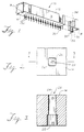
- FIG. 1 shows a general view of an electrical connector 10 which incorporates a presently preferred embodiment of this invention.
- the electrical connector 10 as shown is a header which comprises a connector body 12 molded of a suitable plastic material.
- the body 12 includes a base 14 and integrally molded side walls 16 and standoffs 18. Rows of through holes are preformed in the base 14 during the molding operation.
- FIGS 2 and 3 show further details of one of the through holes 20 of the base 14, which includes a round portion 22 and an out-of-round portion 24 that includes two pairs of opposed faces 26.
- each through hole 20 is formed with a single core pin that forms both the round portion 22 and the out-of-round portion 24, thereby eliminating any internal mating lines (and possible misalignment) within the through hole 20.
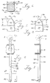
- the electrical connector 10 also includes an array of posts 30, 30'.
- Each of the posts 30, 30' defines a first end 32 and an opposed second end 34.
- the first ends 32 are adapted to be inserted into through holes of a printed circuit board while the second ends 34 are adapted to mate with a mating connector (not shown).
- the four corner posts 30' are provided with a retention feature as described below.
- each of the posts 30 defines a cross-section which comprises two pairs of opposed post faces 38 that intersect at post edges 40 extending parallel to the centerline 36.
- each of the post edges 40 is curved with a radius of curvature which is at least about one fifth of the maximum face to face dimension.
- the maximum face to face dimension is about 0.0635cm (0.025 inches) and the radius of curvature is at least about 0.0127cm (0.005 inches).
- Figures 4 and 7 show one of the posts 30 mounted in a bandolier B which is used to position and retain the posts 30 for forming, plating and press fit operations in the conventional manner.
- Each end of the posts 30, 30' defines a tip 42 which is shaped to provide the advantages described above.
- the features of the tip 42 described below facilitate insertion of the tip 42 into the through hole 20 and provide improved mating between the mating end and the socket of a mating connector (not shown).
- each tip 42 defines four converging tip faces 44 which converge from the body of the post 30 toward a nose 46.
- the nose 46 may be flat or radiused as desired.
- each of the tip faces 44 is shaped as a section of a cylinder and is convex outwardly with a radius of curvature that is preferably greater than the maximum face to face dimension of the post 30.
- Each of the tip faces 44 is aligned with a respective one of the post faces 38 and is joined thereto at a tip-to-body edge 48. Because of the convexity of the tip faces 44, there is a smooth transition between each of the tip faces 44 and the aligned post face 38.
- adjacent ones of the tip faces 44 intersect at tip edges 50 which are convex outwardly and which intersect the radiused post edges 40 at tip-to-body corners 52.
- the convexly shaped tip edges 50 cooperate with the radiused post edges 40 to provide a smooth transition and to substantially eliminate protruding corners that might tend to skive the through hole 20 of the body 12 during assembly.
- an alternate geometry for the tip 42' includes tip faces 44' substantially as described above which meet at a nose 46'.
- intermediate surfaces 56' are provided which taper toward the nose 46'.
- Each of the intermediate surfaces 56' is interposed between two adjacent tip faces 44' such that the intermediate surfaces 56' are rotated by 45 degrees with respect to the tip faces 44'.
- the tip edges 50' curve inwardly toward the tip faces 44'.
- the intermediate surfaces 56' provide a number of advantages. First, they reduce the prominence of the tip-to-body corners 52', thereby reducing skiving problems as described below. Furthermore, because the tip edges 50' curve inwardly toward the tip faces 44', debris tends to be wiped away to the outside of the tip 42' during mating. Furthermore, the shape of the tip faces 44' allows high pressure cleaning of a mating receptacle during mating. In alternative embodiments the tip faces 44' and the intermediate surfaces 56' may be all convex, all planar, or some may be convex and some planar.
- the posts 30 are press fit into the through holes 20 of the body 12, by passing the tips 42, 42' through the through holes 20 in a conventional press-fit operation.
- the tip geometries 42, 42' described above provide advantages during the press-fit operation. Because the tip-to-body corners 52, 52' and the tip-to-body edges 48, 48' are relieved, there is a reduced tendency for the tips 42, 42' to skive plastic out of the body 12 as the tips 42, 42' pass through the through hole 20. Because of the cooperation between the shape of the posts 30 and the shape of the through holes 20, maximum stresses on the body 12 around the through holes 20 are reduced, and maximum insertion forces are reduced as well. Furthermore, because the mating end 54 is shaped as described above, mating forces are reduced as well.
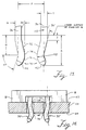
- FIG. 13 shows an enlarged end view of the connector 10 and two of the corner posts 30'.
- Figure 14 shows a cross-sectional view of the electrical connector 10 mounted in a circuit board 60 prior to soldering.
- the circuit board 60 defines top and bottom surfaces 62, 64 and through holes 66 extending therebetween.
- the through holes 66 are generally cylindrical, and the intersection region between the through holes 66 and the surfaces 62, 64 defines corners 68.
- At least one and preferably pairs of the posts 30' are bent to provide a retention feature 70.
- the bent portion of each of the posts 30' defines a first portion 72 which diverges away from the centerline 36 to an apex 74.
- the bent post also defines a second portion 76 which extends from the apex 74 to the tip 42.
- the first and second portions 72, 76 are configured such that the apex 74 is positioned to one side of the centerline 36, but the tip 42 is positioned on the centerline 36.
- the radiused post edges 40 provide rounded contacting surfaces that contact the corners 68 as the retention feature 70 is inserted into the through hole 66.
- each of the retention features 70 creates a latching force tending to pull the electrical connector 10 into contact with the top surface 62.
- the retention features 70 function below the board to latch the electrical connector 10 in place, an audible click may be heard when the electrical connector 10 is seated on the circuit board 60.
- This latching type retention feature as more stable than retention features which rely solely on friction within the through hole 66.
- the retention feature 70 has surprisingly been found to function properly with circuit board through holes 66 having a wide range of diameters, without unacceptable damage to the tin plating that is typically present in the through hole. This surprising result is believed to be directly attributable to the cooperation between the geometry of the first and second portions 72, 76 and the geometry of the radiused post edges 40. The resulting retention feature reduces damage to the through hole plating and functions without any undesirable increase in the length of the post 30' extending below the bottom surface 64 of the circuit board 60.
- the retention feature 70 can be used both with straight headers as shown and right angle headers (not shown). Furthermore, the retention feature 70 can be used on single posts or on pairs of posts as shown in which the apex is 74 offset with respect to the centerline 36. Depending upon the application, the apexes 74 may be offset toward one another, away from one another, or at some angle with respect to one another. Furthermore, the retention feature 70 is well suited for use in headers having one, two, or three or more rows of posts 30.
- the posts 30, 30' may be formed from drawn, radiused phosphor bronze wire such as UNS C51000, Temper 3H.
- the body 12 may be molded of any suitable material such as a glass filled nylon or a liquid crystal polymer.
- Table 1 provides presently preferred dimensions, using reference symbols defined in Figures 5, 6, 8 and 13.
- TABLE 1 Reference Symbol ( Figures ) Dimension Or Angle cms (inches) degrees A 0.05842 (0.023) B 0.04572 (0.018) C 0.02413 (0.0095) D 0.06452 (0.0245) E 0.06452 (0.0245) F 0.254 (0.100) G 0.09652 (0.038) H 0.19558 (0.077) I 0.06452 (0.0245) J 0.0508 (0.020) K 0.29718 (0.117) L1 70° 46 L2 13° 35 R1 0.3302 (0.130) R2 0.01778 (0.007) R3 0.09398 (0.037) R4 0.01524 (0.006) R5 0.1784 (0.055) Note that the length of the tip A is less than the maximum face to face dimension D, E.
- the round portion 22 in this preferred embodiment has a diameter of 0.07036cm (0.0277 inches), and the out-of-round portion 24 in this preferred embodiment defines a maximum diagonal dimension of 0.07036cm (0.0277 inches), and a maximum dimension between opposed faces 26 of 0.05969 cm (0.0235) inches).
- the posts 30, 30' define a maximum diagonal dimension of 0.074168cm (0.0292 inches). These dimensions have been found to provide excellent post retention without excessive post insertion forces or excessive stresses to the body 12.
- the tip 42 is formed in a multi-step operation which combines coining and shearing operations, using vertically moving dies.
- first step an upper one of the tip faces 44 in coined downwardly. This pushes excess metal laterally.
- the two side tip faces 44 shown in profile in Figure 5 are sheared into the desired convex shape.
- the upper and lower tip faces shown in profile in Figure 8 are coined (the upper tip face for the second time and the lower tip face for the first time) to the final convex shape.
- This approach provides the desired tip geometry while requiring only dies that move vertically.
- the first ends 32 are typically tin plated to facilitate soldering, and the second ends 34 are typically gold plated to facilitate mating operations.
- plating details for the first and second ends do not form part of this invention, and are therefore not described in greater detail here.
- This preferred embodiment has been designed for use with through holes 66 having a diameter of 0.1016 cm ⁇ (0.040 ⁇ 0.003 inches) in a circuit board 60 having a thickness of 0.15748 cm ⁇ 0.01778 cm (0.062 ⁇ 0.007 inches). Throughout these tolerance ranges the connector 10 can be inserted with an insertion force of no more than 4.54 kg (10 pounds), and adequate retention forces are obtained. Surprisingly, this has been achieved with stiff posts of the type described above, without damage to the tin plating at the corners 68.
- the present invention may readily be adapted to square posts of other dimensions and to rectangular posts.
- Other forming techniques such as rolling and cutting operations may be used to form the tip, and the radiused post edges may be compressively or otherwise formed only in desired regions of the post.
Abstract

Description
- This invention relates to electrical connectors of the type having a connector body and a plurality of posts extending out of one side of the connector body for mounting to a circuit board. In particular, this invention relates to an improved retention feature for such electrical connectors for temporarily holding the electrical connector in place on a printed circuit board prior to soldering.
- US-A-4 847 588 discloses an electrical connector with a retention feature in which the posts of the connector are offset in the form of a crimp to create frictional forces against the side wall of the through hole of the circuit board onto which the electrical connector is mounted. The discloses retention feature relies entirely on friction, and does not provide any latching force tending to secure the electrical connector in position on the circuit board.
- In another type of retention feature for electrical connectors individual pins of the connector are formed to create a latching force against the bottom surface of the circuit board on which the electrical connector is mounted. See for example US-A-3 524 108 and JP-U-57-86270. Such below the board retention features can provide an audible click when the connector is seated on the circuit board, and some users regard below the board retention features as more stable.
- When below the board retention features are applied to relatively stiff posts such as posts having a cross sectional dimension of 0.0635 by 0.0635 cm (0.025 by 0.025 inches) problems have been encountered. These problems relate to the fact that the through hole geometry of the circuit board varies within a range of tolerances, and the retention feature must function properly throughout this range. In a below the board retention feature the corners of the post latch against the corner of the through hole. In the past, there has been a tendency with relatively thick and inflexible posts for the retention feature to damage the tin plating of the through hole at the corner of engagement with the post, at least when the through hole is near one edge of the tolerance range. This problem has in the past limited the use of below the board retention features with stiff posts.
- In the past, posts have been press fit into connector bodies such as pin headers. Pin headers often include either shrouded or shroudless plastic bodies which define preformed through holes into which the posts are press fit for retention in order to form a header assembly. The dimensions of the through holes and the posts are selected such that the corners of the posts interfere with the through holes, thereby retaining the posts in the connector body by a force fit.
- In the past, problems have arisen during assembly of posts into such connector bodies. The assembly force required to push a post through a through hole may be undesirably high, and longer posts have experienced buckling due to excessively high assembly forces. Cracking of the plastic body of the connector has also occurred due to large interference forces, which may result in broken shrouds or loose posts. Additionally, plastic material may be skived or driven out of the through hole, accumulating on the tip of the post as it is pushed through the through hole. Such plastic material tends to accumulate on the post tip proper, and can lead to undesirable side effects when soldering the header assembly to a printed circuit board. Poor solder joints have been experienced.
- The present invention is directed to an improved tip geometry that in the preferred embodiments described below, meets the following objectives:
- (1) to reduce or eliminate the amount of plastic that is transferred to the tip of the post as the post is inserted into the connector body;
- (2) to reduce the post assembly forces required to assemble the post in the connector body, thereby reducing or eliminating post buckling;
- (3) to reduce the circumferential stresses on the through hole of the post body and to spread them more evenly, thereby reducing or eliminating breakage of the connector body;
- (4) to provide better receptacle engagement surfaces on the mating end of the post, opposed to the solder end, thereby improving the feel of connector mating by reducing roughness and peak mating forces.
- The present invention consists in an electrical connector as defined in
claim 1. - There is described and claimed in EP-A-0 514 066 from which the present application has been divided an electrical connector of the type including a connector body and a plurality of posts extending out of one side of the connector body for mounting to a circuit board, each of said posts defining a tip, and a centerline, wherein the connector is mounted on a circuit board of the type comprising a pair of spaced, parallel surfaces and a plurality of through holes extending therebetween and intersecting the surfaces at corners, and wherein each of the posts is received in a respective one of the through holes, there being at least one retention feature, each formed on a selected one of the posts, said retention feature comprising a bent portion of the post comprising a first portion extending from the centerline to an apex, and a second portion extending from the apex to the tip, said retention feature being configured such that the apex is situated outside of the respective through hole, and the first portion contacts the circuit board at the respective corner between the through hole and the surface opposite the connector body; said second portion defining at least one contacting surface positioned to contact the circuit board at the respective corner between the through hole and the surface adjacent the connector body as the post is inserted into the respective through hole; characterized in that each of said posts defines two pairs of opposed flat faces and a maximum face to face cross sectional dimension, the second portion extending from the apex to the tip such that the apex is laterally offset from the centerline to a greater extent than is the tip, said contacting surface having a radius of curvature no less than about one fifth of the maximum face to face cross-sectional dimension of the post.
- Embodiments of the present invention will now be described by way of example with reference to the accompanying drawings in which:
- FIGURE 1 is a perspective view of a shrouded header assembly which incorporates a presently preferred embodiment of this invention;
- FIGURE 2 is a top view of one of the through holes formed in the connector body of Figure 1;
- FIGURE 3 is a cross sectional view taken along line 3-3 of Figure 2;
- FIGURE 4 is a front view of one of the posts of the connector of Figure 1, mounted in a bandolier prior to insertion into the connector;
- FIGURE 5 is an enlarged view of the
encircled region 5 of Figure 4; - FIGURE 6 is a cross-sectional view taken along line 6-6 of Figure 4;
- FIGURE 7 is a side view taken along line 7-7 of Figure 4;
- FIGURE 8 is an enlarged view of the
encircled region 8 of Figure 7; - FIGURE 9 is a perspective view of the tip geometry of one of the pins of Figures 5 and 7;
- FIGURE 10 is an end view of the tip of the Figure 9;
- FIGURE 11 is a perspective view of an altenrative tip geometry suitable for use with the connector of Figure 1;
- FIGURE 12 is an end view of the tip of Figure 11;
- FIGURE 13 is an end view showing the configuration of the posts at one of the ends of the connector of Figure 1; and
- FIGURE 14 is a cross sectional view showing the posts of Figure 13 engaged with a printed circuit board prior to soldering.
- Turning now to the drawings, Figure 1 shows a general view of an
electrical connector 10 which incorporates a presently preferred embodiment of this invention. Theelectrical connector 10 as shown is a header which comprises aconnector body 12 molded of a suitable plastic material. Thebody 12 includes abase 14 and integrally moldedside walls 16 andstandoffs 18. Rows of through holes are preformed in thebase 14 during the molding operation. - Figures 2 and 3 show further details of one of the through
holes 20 of thebase 14, which includes around portion 22 and an out-of-round portion 24 that includes two pairs ofopposed faces 26. Preferably, each throughhole 20 is formed with a single core pin that forms both theround portion 22 and the out-of-round portion 24, thereby eliminating any internal mating lines (and possible misalignment) within the throughhole 20. - As shown in Figure 1, the
electrical connector 10 also includes an array ofposts 30, 30'. Each of theposts 30, 30' defines afirst end 32 and an opposedsecond end 34. Thefirst ends 32 are adapted to be inserted into through holes of a printed circuit board while thesecond ends 34 are adapted to mate with a mating connector (not shown). In theconnector 10, the four corner posts 30' are provided with a retention feature as described below. - As shown in Figures 4, 6 and 7, each of the
posts 30 defines a cross-section which comprises two pairs ofopposed post faces 38 that intersect atpost edges 40 extending parallel to thecenterline 36. As shown in Figure 6, each of thepost edges 40 is curved with a radius of curvature which is at least about one fifth of the maximum face to face dimension. In this particular embodiment, the maximum face to face dimension is about 0.0635cm (0.025 inches) and the radius of curvature is at least about 0.0127cm (0.005 inches). Figures 4 and 7 show one of theposts 30 mounted in a bandolier B which is used to position and retain theposts 30 for forming, plating and press fit operations in the conventional manner. - Each end of the
posts 30, 30' defines atip 42 which is shaped to provide the advantages described above. The features of thetip 42 described below facilitate insertion of thetip 42 into the throughhole 20 and provide improved mating between the mating end and the socket of a mating connector (not shown). - In particular, as shown in Figures 5, 8, 9 and 10, each
tip 42 defines fourconverging tip faces 44 which converge from the body of thepost 30 toward anose 46. Thenose 46 may be flat or radiused as desired. In this embodiment each of thetip faces 44 is shaped as a section of a cylinder and is convex outwardly with a radius of curvature that is preferably greater than the maximum face to face dimension of thepost 30. Each of thetip faces 44 is aligned with a respective one of the post faces 38 and is joined thereto at a tip-to-body edge 48. Because of the convexity of the tip faces 44, there is a smooth transition between each of the tip faces 44 and the alignedpost face 38. - As best shown in Figures 9 and 10, adjacent ones of the tip faces 44 intersect at
tip edges 50 which are convex outwardly and which intersect theradiused post edges 40 at tip-to-body corners 52. In this regard, the convexly shaped tip edges 50 cooperate with the radiused post edges 40 to provide a smooth transition and to substantially eliminate protruding corners that might tend to skive the throughhole 20 of thebody 12 during assembly. - Turning now to Figures 11 and 12, an alternate geometry for the
tip 42' includes tip faces 44' substantially as described above which meet at a nose 46'. In this alternate embodiment intermediate surfaces 56' are provided which taper toward the nose 46'. Each of the intermediate surfaces 56' is interposed between two adjacent tip faces 44' such that the intermediate surfaces 56' are rotated by 45 degrees with respect to the tip faces 44'. In this embodiment the tip edges 50' curve inwardly toward the tip faces 44'. - The intermediate surfaces 56' provide a number of advantages. First, they reduce the prominence of the tip-to-body corners 52', thereby reducing skiving problems as described below. Furthermore, because the tip edges 50' curve inwardly toward the tip faces 44', debris tends to be wiped away to the outside of the
tip 42' during mating. Furthermore, the shape of the tip faces 44' allows high pressure cleaning of a mating receptacle during mating. In alternative embodiments the tip faces 44' and the intermediate surfaces 56' may be all convex, all planar, or some may be convex and some planar. - In order to assemble the
electrical connector 10 theposts 30 are press fit into the throughholes 20 of thebody 12, by passing thetips holes 20 in a conventional press-fit operation. The tip geometries 42, 42' described above provide advantages during the press-fit operation. Because the tip-to-body corners 52, 52' and the tip-to-body edges 48, 48' are relieved, there is a reduced tendency for thetips body 12 as thetips hole 20. Because of the cooperation between the shape of theposts 30 and the shape of the throughholes 20, maximum stresses on thebody 12 around the throughholes 20 are reduced, and maximum insertion forces are reduced as well. Furthermore, because the mating end 54 is shaped as described above, mating forces are reduced as well. - Once the
electrical connector 10 has been assembled by press fitting theposts 30 into thebody 12, a retention feature can be added to selected ones of theposts 30 to retain theelectrical connector 10 temporarily in place in a circuit board prior to soldering. Figure 13 shows an enlarged end view of theconnector 10 and two of the corner posts 30'. Figure 14 shows a cross-sectional view of theelectrical connector 10 mounted in acircuit board 60 prior to soldering. Thecircuit board 60 defines top andbottom surfaces holes 66 extending therebetween. The through holes 66 are generally cylindrical, and the intersection region between the throughholes 66 and thesurfaces corners 68. - As shown in Figure 13, at least one and preferably pairs of the posts 30' are bent to provide a retention feature 70. The bent portion of each of the posts 30' defines a
first portion 72 which diverges away from thecenterline 36 to an apex 74. The bent post also defines asecond portion 76 which extends from the apex 74 to thetip 42. As shown in Figure 12, the first andsecond portions centerline 36, but thetip 42 is positioned on thecenterline 36. The radiused post edges 40 provide rounded contacting surfaces that contact thecorners 68 as the retention feature 70 is inserted into the throughhole 66. When theconnector 10 is installed on the circuit board 60 (Figure 14), theapexes 74 are positioned below thebottom surface 64. In this way, each of the retention features 70 creates a latching force tending to pull theelectrical connector 10 into contact with thetop surface 62. - Because the retention features 70 function below the board to latch the
electrical connector 10 in place, an audible click may be heard when theelectrical connector 10 is seated on thecircuit board 60. Some users regard this latching type retention feature as more stable than retention features which rely solely on friction within the throughhole 66. The retention feature 70 has surprisingly been found to function properly with circuit board throughholes 66 having a wide range of diameters, without unacceptable damage to the tin plating that is typically present in the through hole. This surprising result is believed to be directly attributable to the cooperation between the geometry of the first andsecond portions bottom surface 64 of thecircuit board 60. - The retention feature 70 can be used both with straight headers as shown and right angle headers (not shown). Furthermore, the retention feature 70 can be used on single posts or on pairs of posts as shown in which the apex is 74 offset with respect to the
centerline 36. Depending upon the application, theapexes 74 may be offset toward one another, away from one another, or at some angle with respect to one another. Furthermore, the retention feature 70 is well suited for use in headers having one, two, or three or more rows ofposts 30. - Simply by way of example, the following details of construction have been found suitable in one application. Of course, these details are not intended to limit the scope of this invention, because other applications will often require other specific geometries or materials.
- With respect to materials, the
posts 30, 30' may be formed from drawn, radiused phosphor bronze wire such as UNS C51000, Temper 3H. Thebody 12 may be molded of any suitable material such as a glass filled nylon or a liquid crystal polymer. - With respect to dimensions, Table 1 provides presently preferred dimensions, using reference symbols defined in Figures 5, 6, 8 and 13.
TABLE 1 Reference Symbol (Figures ) Dimension Or Angle cms (inches) degrees A 0.05842 (0.023) B 0.04572 (0.018) C 0.02413 (0.0095) D 0.06452 (0.0245) E 0.06452 (0.0245) F 0.254 (0.100) G 0.09652 (0.038) H 0.19558 (0.077) I 0.06452 (0.0245) J 0.0508 (0.020) K 0.29718 (0.117) L₁ 70° 46 L₂ 13° 35 R₁ 0.3302 (0.130) R₂ 0.01778 (0.007) R₃ 0.09398 (0.037) R₄ 0.01524 (0.006) R₅ 0.1784 (0.055) Note that the length of the tip A is less than the maximum face to face dimension D, E. - The
round portion 22 in this preferred embodiment has a diameter of 0.07036cm (0.0277 inches), and the out-of-round portion 24 in this preferred embodiment defines a maximum diagonal dimension of 0.07036cm (0.0277 inches), and a maximum dimension between opposed faces 26 of 0.05969 cm (0.0235) inches). Theposts 30, 30' define a maximum diagonal dimension of 0.074168cm (0.0292 inches). These dimensions have been found to provide excellent post retention without excessive post insertion forces or excessive stresses to thebody 12. - Preferably, the
tip 42 is formed in a multi-step operation which combines coining and shearing operations, using vertically moving dies. In the first step an upper one of the tip faces 44 in coined downwardly. This pushes excess metal laterally. Then the two side tip faces 44 shown in profile in Figure 5 are sheared into the desired convex shape. Finally, the upper and lower tip faces shown in profile in Figure 8 are coined (the upper tip face for the second time and the lower tip face for the first time) to the final convex shape. This approach provides the desired tip geometry while requiring only dies that move vertically. - The first ends 32 are typically tin plated to facilitate soldering, and the second ends 34 are typically gold plated to facilitate mating operations. However, plating details for the first and second ends do not form part of this invention, and are therefore not described in greater detail here.
- This preferred embodiment has been designed for use with through
holes 66 having a diameter of 0.1016 cm ± (0.040 ± 0.003 inches) in acircuit board 60 having a thickness of 0.15748 cm ± 0.01778 cm (0.062 ± 0.007 inches). Throughout these tolerance ranges theconnector 10 can be inserted with an insertion force of no more than 4.54 kg (10 pounds), and adequate retention forces are obtained. Surprisingly, this has been achieved with stiff posts of the type described above, without damage to the tin plating at thecorners 68. - The present invention may readily be adapted to square posts of other dimensions and to rectangular posts. Other forming techniques such as rolling and cutting operations may be used to form the tip, and the radiused post edges may be compressively or otherwise formed only in desired regions of the post.
Claims (9)
- An electrical connector (10) of the type including a connector body (12) and at least one post (30,30') extending out of at least one side of the connector body (12), wherein the post defines a tip, wherein the post defines two pairs of opposed post faces (38) that intersect at edges extending along the post, and wherein the post defines a maximum face to face dimension between two of the opposed post faces, the connector being characterized by:
four tip faces (44) which converge toward a tip nose (46), each tip face being aligned with a respective one of the post faces (38);
wherein at least one of the tip faces (44) is convex outwardly; and
wherein the edges between the post faces (38) adjacent to the tip (42) are curved with a radius of curvature greater than about one fifth the maximum face to face dimension. - An electrical connector (10) as claimed in claim 1, further characterized in that the opposed post faces (38) in each pair are separated by an equal distance.
- An electrical connector (10) as claimed in claim 2, further characterized in that the opposed post faces in each pair are separated by about 0.0635 cm (0.025 inches), and wherein the radius of curvature (R1) is greater than about 0.0127 cm (0.005 inches).
- An electrical connector (10) as claimed in claim 3, further characterized in that the tip faces (44) are each convexly curved with a radius of curvature greater than the maximum face to face dimension.
- An electrical connector (10) claimed in claim 1, further characterized in that the edges between the post faces are curved with a radius of curvature of about 0.01524cm (0.006 inches).
- An electrical connector (10) as claimed in claim 1, further characterized in that the tip (42) defines a length, and wherein the length is less than the maximum face to face dimension.
- An electrical connector (10) as claimed in claim 6, further characterized in that the opposed post faces in each pair are separated by 0.0635 cm (0.025 inches) and wherein the radius of curvature is greater than about 0.0127 cm (0.005 inches).
- An electrical connector as claimed in claim 1, further characterized in that the post (30,30') defines a mating end (34), opposed to the tip, for interconnection with a mating connector, and wherein the mating end (34) defines four additional tip faces which converge toward the mating end, each additional tip face being aligned with a respective one of the post faces (38), at least one additional tip face being convex outwardly, each of the edges between the post faces (38) adjacent to the mating end (34) being curved with a radius of curvature greater than about one-fifth the maximum face to face dimension
- An electrical connector as claimed in claim 1, further characterized in that the connector body (12) defines preformed through holes (66) which receive the posts (30,30'), wherein the preformed through holes (66) define two portions of different cross-sectional dimensions, and wherein the preformed through holes (66) are free of internal mating lines.
Applications Claiming Priority (5)
| Application Number | Priority Date | Filing Date | Title |
|---|---|---|---|
| US701929 | 1985-02-15 | ||
| US70343391A | 1991-05-17 | 1991-05-17 | |
| US703433 | 1991-05-17 | ||
| US07/701,929 US5122075A (en) | 1991-05-17 | 1991-05-17 | Electrical connector with improved retention feature |
| EP92304040A EP0514066B1 (en) | 1991-05-17 | 1992-05-05 | Electrical connector with improved retention feature |
Related Parent Applications (1)
| Application Number | Title | Priority Date | Filing Date |
|---|---|---|---|
| EP92304040.6 Division | 1992-05-05 |
Publications (2)
| Publication Number | Publication Date |
|---|---|
| EP0660443A1 true EP0660443A1 (en) | 1995-06-28 |
| EP0660443B1 EP0660443B1 (en) | 1997-10-22 |
Family
ID=27106873
Family Applications (2)
| Application Number | Title | Priority Date | Filing Date |
|---|---|---|---|
| EP92304040A Expired - Lifetime EP0514066B1 (en) | 1991-05-17 | 1992-05-05 | Electrical connector with improved retention feature |
| EP95200108A Expired - Lifetime EP0660443B1 (en) | 1991-05-17 | 1992-05-05 | Electrical connector |
Family Applications Before (1)
| Application Number | Title | Priority Date | Filing Date |
|---|---|---|---|
| EP92304040A Expired - Lifetime EP0514066B1 (en) | 1991-05-17 | 1992-05-05 | Electrical connector with improved retention feature |
Country Status (3)
| Country | Link |
|---|---|
| EP (2) | EP0514066B1 (en) |
| JP (1) | JPH05174886A (en) |
| DE (2) | DE69207261T2 (en) |
Families Citing this family (4)
| Publication number | Priority date | Publication date | Assignee | Title |
|---|---|---|---|---|
| DE4218431C2 (en) * | 1992-06-04 | 1995-04-20 | Cannon Electric Gmbh | Device for connecting a connector to a circuit board |
| GB2271221B (en) * | 1992-09-30 | 1996-07-03 | Thomas & Betts Corp | Electrical connector |
| DE4321065A1 (en) * | 1993-06-24 | 1995-01-19 | Phoenix Contact Gmbh & Co | Connecting strip |
| JP6960748B2 (en) * | 2017-03-07 | 2021-11-05 | ヒロセ電機株式会社 | Electrical connector and electrical connector assembly |
Citations (4)
| Publication number | Priority date | Publication date | Assignee | Title |
|---|---|---|---|---|
| FR2450510A1 (en) * | 1979-02-28 | 1980-09-26 | Souriau & Cie | Low insertion force connector electrode pair - has dimensions defined by given formula to accommodate mfg. tolerance limits |
| US4557549A (en) * | 1980-06-30 | 1985-12-10 | The Charles Stark Draper Laboratory, Inc. | Connector device |
| US4679890A (en) * | 1984-06-25 | 1987-07-14 | American Telephone And Telegraph Company, At&T Bell Laboratories | Connector contact terminal |
| EP0232103A2 (en) * | 1986-01-29 | 1987-08-12 | E.I. Du Pont De Nemours And Company | Improved electrical plug pin and receptacle arrangement for plug and socket connectors |
Family Cites Families (3)
| Publication number | Priority date | Publication date | Assignee | Title |
|---|---|---|---|---|
| US3162721A (en) * | 1960-07-26 | 1964-12-22 | Illinois Tool Works | Component lead-locking arrangement |
| NL6612497A (en) * | 1966-09-06 | 1968-03-07 | ||
| CA1282847C (en) * | 1986-03-05 | 1991-04-09 | Ray C. Doutrich | Electrical connector with pin retention feature |
-
1992
- 1992-05-05 DE DE69207261T patent/DE69207261T2/en not_active Expired - Lifetime
- 1992-05-05 EP EP92304040A patent/EP0514066B1/en not_active Expired - Lifetime
- 1992-05-05 DE DE69222874T patent/DE69222874T2/en not_active Expired - Lifetime
- 1992-05-05 EP EP95200108A patent/EP0660443B1/en not_active Expired - Lifetime
- 1992-05-18 JP JP4148928A patent/JPH05174886A/en active Pending
Patent Citations (4)
| Publication number | Priority date | Publication date | Assignee | Title |
|---|---|---|---|---|
| FR2450510A1 (en) * | 1979-02-28 | 1980-09-26 | Souriau & Cie | Low insertion force connector electrode pair - has dimensions defined by given formula to accommodate mfg. tolerance limits |
| US4557549A (en) * | 1980-06-30 | 1985-12-10 | The Charles Stark Draper Laboratory, Inc. | Connector device |
| US4679890A (en) * | 1984-06-25 | 1987-07-14 | American Telephone And Telegraph Company, At&T Bell Laboratories | Connector contact terminal |
| EP0232103A2 (en) * | 1986-01-29 | 1987-08-12 | E.I. Du Pont De Nemours And Company | Improved electrical plug pin and receptacle arrangement for plug and socket connectors |
Also Published As
| Publication number | Publication date |
|---|---|
| DE69222874T2 (en) | 1998-02-26 |
| EP0514066A1 (en) | 1992-11-19 |
| EP0514066B1 (en) | 1996-01-03 |
| DE69222874D1 (en) | 1997-11-27 |
| EP0660443B1 (en) | 1997-10-22 |
| DE69207261D1 (en) | 1996-02-15 |
| JPH05174886A (en) | 1993-07-13 |
| DE69207261T2 (en) | 1996-08-01 |
Similar Documents
| Publication | Publication Date | Title |
|---|---|---|
| US4874338A (en) | Receptacle box terminal with improved contact area | |
| US5139446A (en) | Electrical connector assembly | |
| EP0664581B1 (en) | Low profile board to board connector | |
| US5584709A (en) | Printed circuit board mounted electrical connector | |
| US5122075A (en) | Electrical connector with improved retention feature | |
| EP0543278B1 (en) | Low profile electrical connector | |
| US6312296B1 (en) | Electrical connector having enhanced retention of contacts in a housing | |
| EP0660445B1 (en) | Electrical connector with improved contact retention | |
| US5702257A (en) | Electrical connector and terminal therefor | |
| US4984996A (en) | Printed circuit board edge connector | |
| US5184962A (en) | Electrical spring contact | |
| US5571033A (en) | Electrical connector having press-fit contacts for circuit board mounting | |
| EP0499431B1 (en) | Lanced hold-downs | |
| US6984135B2 (en) | Press fit pin | |
| US6554659B2 (en) | Connector contact and method of manufacturing the same | |
| EP0660443B1 (en) | Electrical connector | |
| US4778396A (en) | Electrical connector having compliant posts and improved insertion characteristics | |
| US5322461A (en) | Electrical connector with posts having improved tip geometry | |
| US5194022A (en) | Elecrical connector | |
| US5102356A (en) | Electrical connector having board retention means | |
| CA1310382C (en) | Miniature barrel female terminal | |
| EP0139786B1 (en) | Press fit connector insulator and contact | |
| EP0465948B1 (en) | Compliant terminal pin | |
| EP0354064A2 (en) | Multi-pin elecrical connector of low insertion force type | |
| WO1990007806A1 (en) | Electrical connector |
Legal Events
| Date | Code | Title | Description |
|---|---|---|---|
| PUAI | Public reference made under article 153(3) epc to a published international application that has entered the european phase |
Free format text: ORIGINAL CODE: 0009012 |
|
| AC | Divisional application: reference to earlier application |
Ref document number: 514066 Country of ref document: EP |
|
| AK | Designated contracting states |
Kind code of ref document: A1 Designated state(s): DE FR GB |
|
| 17P | Request for examination filed |
Effective date: 19951228 |
|
| GRAG | Despatch of communication of intention to grant |
Free format text: ORIGINAL CODE: EPIDOS AGRA |
|
| 17Q | First examination report despatched |
Effective date: 19961106 |
|
| GRAH | Despatch of communication of intention to grant a patent |
Free format text: ORIGINAL CODE: EPIDOS IGRA |
|
| GRAH | Despatch of communication of intention to grant a patent |
Free format text: ORIGINAL CODE: EPIDOS IGRA |
|
| RBV | Designated contracting states (corrected) |
Designated state(s): DE FR GB |
|
| GRAA | (expected) grant |
Free format text: ORIGINAL CODE: 0009210 |
|
| AC | Divisional application: reference to earlier application |
Ref document number: 514066 Country of ref document: EP |
|
| AK | Designated contracting states |
Kind code of ref document: B1 Designated state(s): DE FR GB |
|
| ET | Fr: translation filed | ||
| REF | Corresponds to: |
Ref document number: 69222874 Country of ref document: DE Date of ref document: 19971127 |
|
| PLBE | No opposition filed within time limit |
Free format text: ORIGINAL CODE: 0009261 |
|
| STAA | Information on the status of an ep patent application or granted ep patent |
Free format text: STATUS: NO OPPOSITION FILED WITHIN TIME LIMIT |
|
| 26N | No opposition filed | ||
| PGFP | Annual fee paid to national office [announced via postgrant information from national office to epo] |
Ref country code: GB Payment date: 19990406 Year of fee payment: 8 |
|
| PG25 | Lapsed in a contracting state [announced via postgrant information from national office to epo] |
Ref country code: GB Free format text: LAPSE BECAUSE OF NON-PAYMENT OF DUE FEES Effective date: 20000505 |
|
| GBPC | Gb: european patent ceased through non-payment of renewal fee |
Effective date: 20000505 |
|
| PGFP | Annual fee paid to national office [announced via postgrant information from national office to epo] |
Ref country code: FR Payment date: 20110607 Year of fee payment: 20 |
|
| PGFP | Annual fee paid to national office [announced via postgrant information from national office to epo] |
Ref country code: DE Payment date: 20110527 Year of fee payment: 20 |
|
| REG | Reference to a national code |
Ref country code: DE Ref legal event code: R071 Ref document number: 69222874 Country of ref document: DE |
|
| REG | Reference to a national code |
Ref country code: DE Ref legal event code: R071 Ref document number: 69222874 Country of ref document: DE |
|
| PG25 | Lapsed in a contracting state [announced via postgrant information from national office to epo] |
Ref country code: DE Free format text: LAPSE BECAUSE OF EXPIRATION OF PROTECTION Effective date: 20120508 |