EP0683517A2 - Semiconductor device having semiconductor chip bonded to circuit board through bumps and process of mounting thereof - Google Patents
Semiconductor device having semiconductor chip bonded to circuit board through bumps and process of mounting thereof Download PDFInfo
- Publication number
- EP0683517A2 EP0683517A2 EP95106499A EP95106499A EP0683517A2 EP 0683517 A2 EP0683517 A2 EP 0683517A2 EP 95106499 A EP95106499 A EP 95106499A EP 95106499 A EP95106499 A EP 95106499A EP 0683517 A2 EP0683517 A2 EP 0683517A2
- Authority
- EP
- European Patent Office
- Prior art keywords
- semiconductor chip
- area
- set forth
- conductive pattern
- tape
- Prior art date
- Legal status (The legal status is an assumption and is not a legal conclusion. Google has not performed a legal analysis and makes no representation as to the accuracy of the status listed.)
- Granted
Links
Images


Classifications
-
- H—ELECTRICITY
- H01—ELECTRIC ELEMENTS
- H01L—SEMICONDUCTOR DEVICES NOT COVERED BY CLASS H10
- H01L24/00—Arrangements for connecting or disconnecting semiconductor or solid-state bodies; Methods or apparatus related thereto
- H01L24/01—Means for bonding being attached to, or being formed on, the surface to be connected, e.g. chip-to-package, die-attach, "first-level" interconnects; Manufacturing methods related thereto
- H01L24/50—Tape automated bonding [TAB] connectors, i.e. film carriers; Manufacturing methods related thereto
-
- H—ELECTRICITY
- H01—ELECTRIC ELEMENTS
- H01L—SEMICONDUCTOR DEVICES NOT COVERED BY CLASS H10
- H01L21/00—Processes or apparatus adapted for the manufacture or treatment of semiconductor or solid state devices or of parts thereof
- H01L21/02—Manufacture or treatment of semiconductor devices or of parts thereof
- H01L21/04—Manufacture or treatment of semiconductor devices or of parts thereof the devices having at least one potential-jump barrier or surface barrier, e.g. PN junction, depletion layer or carrier concentration layer
- H01L21/50—Assembly of semiconductor devices using processes or apparatus not provided for in a single one of the subgroups H01L21/06 - H01L21/326, e.g. sealing of a cap to a base of a container
- H01L21/60—Attaching or detaching leads or other conductive members, to be used for carrying current to or from the device in operation
-
- H—ELECTRICITY
- H01—ELECTRIC ELEMENTS
- H01L—SEMICONDUCTOR DEVICES NOT COVERED BY CLASS H10
- H01L23/00—Details of semiconductor or other solid state devices
- H01L23/28—Encapsulations, e.g. encapsulating layers, coatings, e.g. for protection
- H01L23/31—Encapsulations, e.g. encapsulating layers, coatings, e.g. for protection characterised by the arrangement or shape
- H01L23/3107—Encapsulations, e.g. encapsulating layers, coatings, e.g. for protection characterised by the arrangement or shape the device being completely enclosed
- H01L23/3121—Encapsulations, e.g. encapsulating layers, coatings, e.g. for protection characterised by the arrangement or shape the device being completely enclosed a substrate forming part of the encapsulation
- H01L23/3128—Encapsulations, e.g. encapsulating layers, coatings, e.g. for protection characterised by the arrangement or shape the device being completely enclosed a substrate forming part of the encapsulation the substrate having spherical bumps for external connection
-
- H—ELECTRICITY
- H01—ELECTRIC ELEMENTS
- H01L—SEMICONDUCTOR DEVICES NOT COVERED BY CLASS H10
- H01L23/00—Details of semiconductor or other solid state devices
- H01L23/28—Encapsulations, e.g. encapsulating layers, coatings, e.g. for protection
- H01L23/31—Encapsulations, e.g. encapsulating layers, coatings, e.g. for protection characterised by the arrangement or shape
- H01L23/3157—Partial encapsulation or coating
- H01L23/3185—Partial encapsulation or coating the coating covering also the sidewalls of the semiconductor body
-
- H—ELECTRICITY
- H01—ELECTRIC ELEMENTS
- H01L—SEMICONDUCTOR DEVICES NOT COVERED BY CLASS H10
- H01L23/00—Details of semiconductor or other solid state devices
- H01L23/48—Arrangements for conducting electric current to or from the solid state body in operation, e.g. leads, terminal arrangements ; Selection of materials therefor
- H01L23/488—Arrangements for conducting electric current to or from the solid state body in operation, e.g. leads, terminal arrangements ; Selection of materials therefor consisting of soldered or bonded constructions
- H01L23/495—Lead-frames or other flat leads
- H01L23/49572—Lead-frames or other flat leads consisting of thin flexible metallic tape with or without a film carrier
-
- H—ELECTRICITY
- H01—ELECTRIC ELEMENTS
- H01L—SEMICONDUCTOR DEVICES NOT COVERED BY CLASS H10
- H01L23/00—Details of semiconductor or other solid state devices
- H01L23/48—Arrangements for conducting electric current to or from the solid state body in operation, e.g. leads, terminal arrangements ; Selection of materials therefor
- H01L23/488—Arrangements for conducting electric current to or from the solid state body in operation, e.g. leads, terminal arrangements ; Selection of materials therefor consisting of soldered or bonded constructions
- H01L23/498—Leads, i.e. metallisations or lead-frames on insulating substrates, e.g. chip carriers
- H01L23/49811—Additional leads joined to the metallisation on the insulating substrate, e.g. pins, bumps, wires, flat leads
- H01L23/49816—Spherical bumps on the substrate for external connection, e.g. ball grid arrays [BGA]
-
- H—ELECTRICITY
- H01—ELECTRIC ELEMENTS
- H01L—SEMICONDUCTOR DEVICES NOT COVERED BY CLASS H10
- H01L24/00—Arrangements for connecting or disconnecting semiconductor or solid-state bodies; Methods or apparatus related thereto
- H01L24/80—Methods for connecting semiconductor or other solid state bodies using means for bonding being attached to, or being formed on, the surface to be connected
- H01L24/86—Methods for connecting semiconductor or other solid state bodies using means for bonding being attached to, or being formed on, the surface to be connected using tape automated bonding [TAB]
-
- H—ELECTRICITY
- H05—ELECTRIC TECHNIQUES NOT OTHERWISE PROVIDED FOR
- H05K—PRINTED CIRCUITS; CASINGS OR CONSTRUCTIONAL DETAILS OF ELECTRIC APPARATUS; MANUFACTURE OF ASSEMBLAGES OF ELECTRICAL COMPONENTS
- H05K3/00—Apparatus or processes for manufacturing printed circuits
- H05K3/30—Assembling printed circuits with electric components, e.g. with resistor
- H05K3/32—Assembling printed circuits with electric components, e.g. with resistor electrically connecting electric components or wires to printed circuits
- H05K3/34—Assembling printed circuits with electric components, e.g. with resistor electrically connecting electric components or wires to printed circuits by soldering
- H05K3/341—Surface mounted components
- H05K3/3431—Leadless components
- H05K3/3436—Leadless components having an array of bottom contacts, e.g. pad grid array or ball grid array components
-
- H—ELECTRICITY
- H01—ELECTRIC ELEMENTS
- H01L—SEMICONDUCTOR DEVICES NOT COVERED BY CLASS H10
- H01L2224/00—Indexing scheme for arrangements for connecting or disconnecting semiconductor or solid-state bodies and methods related thereto as covered by H01L24/00
- H01L2224/73—Means for bonding being of different types provided for in two or more of groups H01L2224/10, H01L2224/18, H01L2224/26, H01L2224/34, H01L2224/42, H01L2224/50, H01L2224/63, H01L2224/71
- H01L2224/732—Location after the connecting process
- H01L2224/73251—Location after the connecting process on different surfaces
- H01L2224/73253—Bump and layer connectors
-
- H—ELECTRICITY
- H01—ELECTRIC ELEMENTS
- H01L—SEMICONDUCTOR DEVICES NOT COVERED BY CLASS H10
- H01L2924/00—Indexing scheme for arrangements or methods for connecting or disconnecting semiconductor or solid-state bodies as covered by H01L24/00
- H01L2924/01—Chemical elements
- H01L2924/01005—Boron [B]
-
- H—ELECTRICITY
- H01—ELECTRIC ELEMENTS
- H01L—SEMICONDUCTOR DEVICES NOT COVERED BY CLASS H10
- H01L2924/00—Indexing scheme for arrangements or methods for connecting or disconnecting semiconductor or solid-state bodies as covered by H01L24/00
- H01L2924/01—Chemical elements
- H01L2924/01006—Carbon [C]
-
- H—ELECTRICITY
- H01—ELECTRIC ELEMENTS
- H01L—SEMICONDUCTOR DEVICES NOT COVERED BY CLASS H10
- H01L2924/00—Indexing scheme for arrangements or methods for connecting or disconnecting semiconductor or solid-state bodies as covered by H01L24/00
- H01L2924/01—Chemical elements
- H01L2924/01013—Aluminum [Al]
-
- H—ELECTRICITY
- H01—ELECTRIC ELEMENTS
- H01L—SEMICONDUCTOR DEVICES NOT COVERED BY CLASS H10
- H01L2924/00—Indexing scheme for arrangements or methods for connecting or disconnecting semiconductor or solid-state bodies as covered by H01L24/00
- H01L2924/01—Chemical elements
- H01L2924/01029—Copper [Cu]
-
- H—ELECTRICITY
- H01—ELECTRIC ELEMENTS
- H01L—SEMICONDUCTOR DEVICES NOT COVERED BY CLASS H10
- H01L2924/00—Indexing scheme for arrangements or methods for connecting or disconnecting semiconductor or solid-state bodies as covered by H01L24/00
- H01L2924/01—Chemical elements
- H01L2924/01033—Arsenic [As]
-
- H—ELECTRICITY
- H01—ELECTRIC ELEMENTS
- H01L—SEMICONDUCTOR DEVICES NOT COVERED BY CLASS H10
- H01L2924/00—Indexing scheme for arrangements or methods for connecting or disconnecting semiconductor or solid-state bodies as covered by H01L24/00
- H01L2924/01—Chemical elements
- H01L2924/01078—Platinum [Pt]
-
- H—ELECTRICITY
- H01—ELECTRIC ELEMENTS
- H01L—SEMICONDUCTOR DEVICES NOT COVERED BY CLASS H10
- H01L2924/00—Indexing scheme for arrangements or methods for connecting or disconnecting semiconductor or solid-state bodies as covered by H01L24/00
- H01L2924/01—Chemical elements
- H01L2924/01079—Gold [Au]
-
- H—ELECTRICITY
- H01—ELECTRIC ELEMENTS
- H01L—SEMICONDUCTOR DEVICES NOT COVERED BY CLASS H10
- H01L2924/00—Indexing scheme for arrangements or methods for connecting or disconnecting semiconductor or solid-state bodies as covered by H01L24/00
- H01L2924/01—Chemical elements
- H01L2924/01082—Lead [Pb]
-
- H—ELECTRICITY
- H01—ELECTRIC ELEMENTS
- H01L—SEMICONDUCTOR DEVICES NOT COVERED BY CLASS H10
- H01L2924/00—Indexing scheme for arrangements or methods for connecting or disconnecting semiconductor or solid-state bodies as covered by H01L24/00
- H01L2924/013—Alloys
- H01L2924/0132—Binary Alloys
- H01L2924/01322—Eutectic Alloys, i.e. obtained by a liquid transforming into two solid phases
-
- H—ELECTRICITY
- H01—ELECTRIC ELEMENTS
- H01L—SEMICONDUCTOR DEVICES NOT COVERED BY CLASS H10
- H01L2924/00—Indexing scheme for arrangements or methods for connecting or disconnecting semiconductor or solid-state bodies as covered by H01L24/00
- H01L2924/10—Details of semiconductor or other solid state devices to be connected
- H01L2924/11—Device type
- H01L2924/14—Integrated circuits
-
- H—ELECTRICITY
- H01—ELECTRIC ELEMENTS
- H01L—SEMICONDUCTOR DEVICES NOT COVERED BY CLASS H10
- H01L2924/00—Indexing scheme for arrangements or methods for connecting or disconnecting semiconductor or solid-state bodies as covered by H01L24/00
- H01L2924/15—Details of package parts other than the semiconductor or other solid state devices to be connected
- H01L2924/151—Die mounting substrate
- H01L2924/153—Connection portion
- H01L2924/1531—Connection portion the connection portion being formed only on the surface of the substrate opposite to the die mounting surface
- H01L2924/15311—Connection portion the connection portion being formed only on the surface of the substrate opposite to the die mounting surface being a ball array, e.g. BGA
-
- H—ELECTRICITY
- H05—ELECTRIC TECHNIQUES NOT OTHERWISE PROVIDED FOR
- H05K—PRINTED CIRCUITS; CASINGS OR CONSTRUCTIONAL DETAILS OF ELECTRIC APPARATUS; MANUFACTURE OF ASSEMBLAGES OF ELECTRICAL COMPONENTS
- H05K2201/00—Indexing scheme relating to printed circuits covered by H05K1/00
- H05K2201/10—Details of components or other objects attached to or integrated in a printed circuit board
- H05K2201/10613—Details of electrical connections of non-printed components, e.g. special leads
- H05K2201/10621—Components characterised by their electrical contacts
- H05K2201/10681—Tape Carrier Package [TCP]; Flexible sheet connector
-
- Y—GENERAL TAGGING OF NEW TECHNOLOGICAL DEVELOPMENTS; GENERAL TAGGING OF CROSS-SECTIONAL TECHNOLOGIES SPANNING OVER SEVERAL SECTIONS OF THE IPC; TECHNICAL SUBJECTS COVERED BY FORMER USPC CROSS-REFERENCE ART COLLECTIONS [XRACs] AND DIGESTS
- Y02—TECHNOLOGIES OR APPLICATIONS FOR MITIGATION OR ADAPTATION AGAINST CLIMATE CHANGE
- Y02P—CLIMATE CHANGE MITIGATION TECHNOLOGIES IN THE PRODUCTION OR PROCESSING OF GOODS
- Y02P70/00—Climate change mitigation technologies in the production process for final industrial or consumer products
- Y02P70/50—Manufacturing or production processes characterised by the final manufactured product
-
- Y—GENERAL TAGGING OF NEW TECHNOLOGICAL DEVELOPMENTS; GENERAL TAGGING OF CROSS-SECTIONAL TECHNOLOGIES SPANNING OVER SEVERAL SECTIONS OF THE IPC; TECHNICAL SUBJECTS COVERED BY FORMER USPC CROSS-REFERENCE ART COLLECTIONS [XRACs] AND DIGESTS
- Y10—TECHNICAL SUBJECTS COVERED BY FORMER USPC
- Y10T—TECHNICAL SUBJECTS COVERED BY FORMER US CLASSIFICATION
- Y10T29/00—Metal working
- Y10T29/49—Method of mechanical manufacture
- Y10T29/49002—Electrical device making
- Y10T29/49117—Conductor or circuit manufacturing
- Y10T29/49121—Beam lead frame or beam lead device
-
- Y—GENERAL TAGGING OF NEW TECHNOLOGICAL DEVELOPMENTS; GENERAL TAGGING OF CROSS-SECTIONAL TECHNOLOGIES SPANNING OVER SEVERAL SECTIONS OF THE IPC; TECHNICAL SUBJECTS COVERED BY FORMER USPC CROSS-REFERENCE ART COLLECTIONS [XRACs] AND DIGESTS
- Y10—TECHNICAL SUBJECTS COVERED BY FORMER USPC
- Y10T—TECHNICAL SUBJECTS COVERED BY FORMER US CLASSIFICATION
- Y10T29/00—Metal working
- Y10T29/49—Method of mechanical manufacture
- Y10T29/49002—Electrical device making
- Y10T29/49117—Conductor or circuit manufacturing
- Y10T29/49124—On flat or curved insulated base, e.g., printed circuit, etc.
- Y10T29/4913—Assembling to base an electrical component, e.g., capacitor, etc.
- Y10T29/49144—Assembling to base an electrical component, e.g., capacitor, etc. by metal fusion
Definitions
- This invention relates to a mounting technology for a semiconductor chip and, more particularly, to a mounting technology for a semiconductor chip through a tape automated bonding on a printed circuit board.
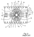
- FIG. 1A A typical example of a process of mounting a semiconductor chip on a film carrier tape available for the TAB (Tape Automated Bonding) technology is illustrated in figures 1A to 1C and 2, and figure 2 shows a layout of the film carrier tape at the stage shown in figure1 A.
- the prior art mounting process starts with preparation of a film carrier tape. Namely, sprocket holes 1, a device hole 2 and separation holes 3 are formed in a base film 4 of insulating material such as, for example, polyimide.
- the portions between the device hole 2 and the separation holes 3 are called as suspenders 4a, and the portions between the separation holes 3 are referred to as bridges 4b.
- the sprocket holes 1 are arranged along side edges of the base film 4, and used for moving and positioning the film carrier tape in a later stage.
- the device hole 2 is wide enough to accommodate a semiconductor chip 5, and metal bumps 5a are formed on electrodes exposed to the upper surface of the semiconductor chip 5 for an inner lead bonding.
- the separation holes 3 are abbreviated as "OLB (Outer Lead Bonding)" holes, and are provided around the device hole 2.
- a metal foil of, for example, copper is laminated on the upper surface of the base film 4, and adhesive paste 6 bonds the metal foil to the upper surface of the base film 4.
- the metal foil is patterned into a plurality of conductive leads 7 by using photo-lithographic technologies.
- Each of the conductive leads 7 is broken down into an inner lead portion, an outer lead portion and a pad portion for electric tests.
- the inner lead portion 6a partially projects into the device hole 2, and is merged into the outer lead portion in the suspender 4a.
- the outer lead portion extends across the separation holes 3, and is merged into the pad portion.
- the conductive leads 7 are covered with gold, tin or solder through galvanization, and the gold film, the tin film or the solder film serves as a protecting film.
- Sprocket wheels conveys the film carrier tape, and the device hole 2 is aligned with the semiconductor chip 5. Then, a bonding tool (not shown) is pressed against the bumps 5a, and heat is applied from the bonding tool to the inner lead portions of the conductive leads 7. Thus, the conductive leads 7 are bonded to the bumps 5a through the thermo-compression bonding technique. An eutectic process may be used for bonding the conductive leads 7 to the bumps 5a. The resultant structure at this stage is illustrated in figures 1A and 2.
- a piece 8 of resin is provided on the upper surface of the semiconductor chip 5 exposed to the device hole 2 as shown in figure 1B, and prevents a circuit pattern formed on the upper surface of the semiconductor chip 5 from undesirable contamination.
- the bridges 4b of the film carrier tape 4 are broken, and the suspenders 4a are separated from the film carrier tape together with the semiconductor chip 5 and the conductive leads 7.
- the manufacturer previously prepares a printed circuit board 9, and a conductive pattern 9a is printed on an insulating rigid board 9b.
- the semiconductor chip 5 and the outer lead portions of the conductive leads 7 are aligned with the conductive pattern 9a, and the outer lead portions are bonded to the conductive pattern 9a through the thermo-compression bonding technique.
- the conductive leads 7 are of the order of 35 microns in thickness, and the outer lead portions of the conductive leads 7 are expected to be accurately patterned and highly coplanar so as to prevent the semiconductor device from a bond lift-off.
- These conditions require a special purpose bonding machine for bonding the outer lead portions of the conductive leads 7 to the conductive pattern 9a of the printed circuit board 9, and the mounting system including such a special purpose machine is hardly available for other semiconductor devices of a different type such as QFP (****** *******************) mounted through a concurrent reflow step. This results in a large amount of the plant and equipment investment which in turn increases the production cost of the semiconductor device.
- QFP is desirable for the productivity because of the concurrent reflow.
- the pitch of the outer lead portions is minimized at 0.4 millimeter, and sets a limit on the interface of an integrated circuit.
- An attractive break-through technology is introduced in NIKKEI MICRODEVICES, 1994, May, pages 58 to 64, and is called as the ball grid array.
- a large number of solder-bumps are arrayed on a back surface of a GBA-type package, and are rather dense than the QFP.
- QFP requires the minimum pitch of 0.4 millimeter for 220 signal pins on a square area of 23 to 24 millimeters.
- the GBA realizes the 220 signal pins on the same area at 1.5 millimeter pitch. This means that the GBA technology can decrease the occupation area of the signal pins and, accordingly, the lengths of the signal paths. The decreased signal paths improve device characteristics.
- the GBA technology is very attractive to manufacturers, and a multi-level printed circuit board is used for the GBA package.
- the multi-level printed circuit board is formed from ceramics plates or films such as the tape automated bonding tapes.
- Japanese Patent Publication of Unexamined Application No. 63-34936 discloses the multi-level printed circuit board formed from the tape automated bonding tapes.
- a conductive pattern is formed on a major surface of a base film, and is electrically connected through through-holes formed in the base film to terminals on the back surface. The terminals are connected to a printed circuit board.
- the present invention proposes to connect conductive leads through bumps to a conductive pattern.
- a semiconductor device comprising: a) a semiconductor chip having an electric circuit connected to electrodes exposed to a surface of said semiconductor chip; b) a frame-like film separated from a tape automated bonding tape; c) a plurality of conductive leads having outer end portions and inner end portions connected to said electrodes of said semiconductor chips; and c) a conductive pattern formed on a board means, and is characterized by d) bumps formed on said outer end portions of said conductive leads, respectively, and bonded to said conductive pattern for providing electrical connections between said outer end portions of said conductive leads and said conductive pattern.
- a process of mounting a semiconductor chip on a mounting board means comprising the steps of: a) preparing a semiconductor chip, a mounting board means and a tape automated bonding tape including a film carrier tape having a first area and a second area separable from the first area and a conductive pattern having inner leads and pads electrically connected to the inner leads formed in the second area; b) bonding the inner leads to electrodes of the semiconductor chip; c) forming conductive bumps on the pads; d) separating the second area having the conductive pattern electrically connected to the electrodes of the semiconductor chip from the first area; and e) bonding the bumps to a conductive pattern on the mounting board means.
- the electrodes connected to the conductive leads may be covered with resin before the formation of the bumps.
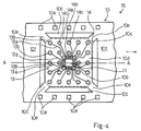
- FIGS 3A to 3E and 4 illustrate a mounting process embodying the present invention, and figures 3A to 3E show cross sections taken along line A-A of figure 4. However, a resin coating is omitted from the structure shown in figure 4 for the sake of simplicity.
- the mounting process starts with preparation of a flexible film carrier tape 10, and two lines of sprocket holes 10a are formed along the two side edges of the flexible film carrier 10.
- Device holes 10b are further formed at intervals, and are slightly wider than a semiconductor chip 11.
- Four elongated separation holes 10c are provided around each of the device holes 10b, and a suspender area 10d are connected through bridging areas 10e to a frame area 10f.
- the frame area 10f serves as a first area
- the suspender area 10e serves as a second area in this instance.
- Adhesive compound 12 bonds a conductive metal foil of, for example, copper to a surface of the flexible film carrier 10, and the conductive metal foil is patterned into a plurality of conductive leads 13 by using photo-lithographic techniques.
- Each of the conductive leads 13 is broken down into an inner lead portion 13a projecting into the device hole 10b and a pad portion 13b merged with the inner lead portion 13a, and the pad portions 13b are arranged in an array as will be better seen in figure 4.
- the pad portions 13b are arrayed at intervals of 1.0 millimeter.
- At least the conductive leads 13 and the exposed suspender area 10d are coated with cover-resist, and the cover-resist film is patterned so as to expose center areas of the pad portions 13b and the inner peripheral sub-area of the suspender area 10d.
- Broken lines 14a, 14b and 14c respectively indicate an outer periphery and an inner periphery of the cover-resist layer 14 and small holes exposing parts of the pad portions 13b in figure 4.
- An initial elastic modulus of the cover-resist 14 is less than a tenth of that of the base film 10, and the flatness of the base film 10 is acceptable for later stages. It is recommendable to use a cover-resist 14 having the initial elastic modulus about 1 twentieth so as to make the warp of the base film 10 negligible. On the other hand, if an epoxy resin is used as the cover-resist 14, the initial elastic modulus is of the order of 200 kg/mm2, and the warp of the base film 10 is serious in the later stages.
- the openings of the cover-resist 14 are slightly smaller in area than the pad portions 13b. If the pad portions 13b are 0.6 millimeter in diameter, the openings in the cover-resist 14 are about 0.5 millimeter in diameter. It is not necessary to plate the conductive leads 13 on the suspender area 10d, and the omission of the plating stage decreases the production cost of the semiconductor device.
- the pad portions 13b are arranged closer to the separation holes 10c, and test pads and plated wirings are formed.
- the pad portions 13b are available as check pads for a short-circuit of the wiring pattern, and this is conducive to scaling down of the semiconductor device.
- the tape-automated bonding tape 15 is set into an inner bonding machine, and rotating sprockets 16a are sequentially brought into meshing engagement with the sprocket holes 10a so as to convey the tape-automated bonding tape 15 in synchronism with a carrier tape (not shown) carrying the semiconductor chips 11.
- the semiconductor chip 11 has a plurality of electrodes 11a connected to an electric circuit fabricated in the semiconductor chip 11, and the inner bonding machine aligns the inner lead portions 13a with the electrodes 11a under a thermo-compressing tool 16b.
- the thermo-compressing tool 16b presses the inner lead portions 13a against the electrodes 11a, and the inner lead portions 13a are bonded to the electrodes 11a through the thermo-compression.
- the resultant structure of this stage is illustrated in figure 3B.
- a piece of resin 17 covers the connections between the electrodes 11a and the inner lead portions 13a, and fills a space left between the semiconductor chip 11 and the base film 10 as shown in figure 3C.
- the piece of resin 17 further covers the inner peripheral sub-area of the suspender area 10d, and is merged with the cover-resist 14. For this reason, the piece of resin 17 is wider than the device hole 10b by at least one millimeter. It is recommendable to regulate the height of the piece of resin 17 equal to be not greater than 250 microns with respect to the upper surface of the semiconductor chip 11.
- the piece of resin 17 prevents the connection between the electrodes 11a and the inner lead portions 13a from oxidation and contamination, and securely fixes the semiconductor chip 11 to the inner lead portions 13a and the suspender area 10d of the tape-automated bonding tape.
- solder balls are provided on the pad portions 13b, and are melted in nitrogen atmosphere. Then, the solder balls are bonded to the pad portions 13b, and bumps 18 are provided on the pad portions 13b, respectively.
- the bumps 18 are larger in diameter than the openings in the cover-resist 14. In this instance, the bumps are 0.8 millimeter in diameter.
- bumps 18 Another formation technique for the bumps 18 is print. If the pad portions 13b are covered with thick oxide films, a flux is necessary. However, if the flux is not used, it is not necessary to make the openings in the cover-resist 14 smaller than the pad portions 13b.
- the bridging areas 10e are cut, and the suspender area 10d and the semiconductor chip 11 are separated from the frame area 10f as shown in figure 3D.
- the conductive leads 13 connected to the semiconductor chip 11 are subjected to an electric selection.
- the bumps 18 are aligned with a conductive pattern 19a of a printed circuit board 19b.
- the bumps 18 are bonded to the conductive pattern 19a through a concurrent reflow stage.
- the reflow machine is commonly available for other types of semiconductor chips, and a special purpose outer bonding machine is not required. For this reason, the semiconductor device according to the present invention is economically mounted on the printed circuit board 19b.
- the bumps 18 are securely bonded to the conductive pattern 19a, and improves the yield of the semiconductor device.
- a modification of the first embodiment has a heat radiating plate attached to the semiconductor chip 11 by means of adhesive compound having a large coefficient of heat transfer.
- Another modification may further has a heat sink attached to the heat radiating plate by means of the adhesive compound. The heat radiating plate and the heat sink are successively attached to the semiconductor chip 11 after the mount on the printed circuit board 19b.
- the bumps 18 securely fix the pad portions 13b to the conductive pattern 19a of the printed circuit board 19b without a special purpose machine, and the production cost, the yield and the reliability of the semiconductor device is surely improved.
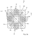
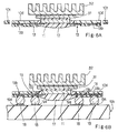
- FIG. 5A and 5B shows essential stages of another mounting process embodying the present invention.
- a heat radiating bump 21, a heat radiating plate 22a and a heat sink 22b are provided for the semiconductor device, and other components are similar to those of the first embodiment. For this reason, the other components are labeled with the same references as the corresponding parts of the semiconductor device implementing the first embodiment without detailed description.
- the process sequence implementing the second embodiment also starts with preparation of a tape-automated bonding tape 23, the semiconductor device 11, the printed circuit board 19b, the heat radiating plate 22a and the heat sink 22b, and are similar to the mounting process except for the followings.
- the tape-automated bonding tape 23 is similar to the tape-automated bonding tape 15 except for a suspended lead 24.
- the suspended lead 24 is concurrently formed from the same metal foil as the conductive leads 13, and has a central portion 24a over the semiconductor chip 11 and bridging portions 24b merged with the central portion 24a.
- the cover-resist 14 extends over the suspended lead 24, and further covers it. In order to clearly discriminate the cover-resist 14, the cover-resist 14 is indicated by hatch lines in figure 5A.
- An opening 25 is formed in the cover-resist 14, and exposes a part of the central portion 24a. It is desirable for the opening 25 to be equal in diameter to the openings on the pad portions 13b, because the opening 25 is concurrently formed in the cover-resist 14 together with the openings over the pad portions 13b. However, if the bumps are formed through a printing process, it is not necessary to regulates the opening 25 to the diameter of the openings on the pad portions 13b.
- a kind of resin 25 is supplied from a gap between the suspended lead, and spreads between the suspended lead 24 and the semiconductor chip 11 through the capillary phenomenon. In other words, it is recommendable to select the resin 25 having the viscosity small enough to be spread through the capillary phenomenon.
- the suspended lead 24 is supported by means of, for example, a vacuum nozzle during the supply of the resin 25, the resin 24 sufficiently spreads over the space between the suspended lead 24 and the semiconductor chip 11.
- the heat radiating bump 21 keeps the semiconductor chip 11 in parallel to the surface of the printed circuit board 19b.
- the heat radiating plate 22a of aluminum is bonded to the semiconductor chip 11 by means of an adhesive paste layer 26a with a large coefficient of heat transfer.
- the heat sink 22b is further bonded to the heat radiating plate 22a by means of an adhesive paste layer 26b having a large coefficient of heat transfer.
- the attachment of the heat radiating plate 22a and the heat sink 22b is carried out after the bonding stage between the bumps 18 and 21 and the conductive pattern 19a.
- the heat radiating plate 22a and the heat sink 22b are available for the semiconductor device implementing the first embodiment as described hereinbefore, it is recommendable to bond the heat radiating plate 22a to not only the semiconductor chip 11 but also the base film 10, because the weight pushes down the semiconductor chip in the absence of the heat radiating bump 21.
- a solder plate or a resin column may be previously provided on the printed circuit board 19b, and the solder plate or the resin column support the semiconductor chip at the piece of resin 25.
- the semiconductor device implementing the second embodiment achieves all the advantages of the first embodiment and large heat radiation. Namely, the semiconductor device according to the present invention does not need a printed circuit board with through-holes, a ceramics plate with through-holes and a TAB tape with through-holes, and a economical standard TAB tape is available.
- the bumps 18 and 21 are concurrently bonded to the conductive pattern 19a through a reflow, and the semiconductor device according to the present invention can share a reflow system with other types of semiconductor devices.
- the pad portions 13b may be electrically connected through the bumps 18 to a conductive pattern formed on a flexible film.
- the inner lead portions are concurrently bonded to the electrodes on the semiconductor chip by using the tool in the above described embodiments.
- the electrodes may be sequentially bonded to the electrodes.
- figure 6A illustrates a heat radiating plate 31 and a heat sink 32 bonded to the semiconductor chip 11 connected to the conductive leads 13. Thereafter, the bumps are formed on the pad portions 13b, and the bumps 18 are bonded to the conductive pattern 19a of the printed circuit board 19b as shown in figure 6B.
Abstract
Description
- This invention relates to a mounting technology for a semiconductor chip and, more particularly, to a mounting technology for a semiconductor chip through a tape automated bonding on a printed circuit board.
- A typical example of a process of mounting a semiconductor chip on a film carrier tape available for the TAB (Tape Automated Bonding) technology is illustrated in figures 1A to 1C and 2, and figure 2 shows a layout of the film carrier tape at the stage shown in figure1 A.
- The prior art mounting process starts with preparation of a film carrier tape. Namely, sprocket
holes 1, adevice hole 2 andseparation holes 3 are formed in abase film 4 of insulating material such as, for example, polyimide. The portions between thedevice hole 2 and theseparation holes 3 are called assuspenders 4a, and the portions between theseparation holes 3 are referred to asbridges 4b. - The
sprocket holes 1 are arranged along side edges of thebase film 4, and used for moving and positioning the film carrier tape in a later stage. Thedevice hole 2 is wide enough to accommodate asemiconductor chip 5, andmetal bumps 5a are formed on electrodes exposed to the upper surface of thesemiconductor chip 5 for an inner lead bonding. Theseparation holes 3 are abbreviated as "OLB (Outer Lead Bonding)" holes, and are provided around thedevice hole 2. - Subsequently, a metal foil of, for example, copper is laminated on the upper surface of the
base film 4, andadhesive paste 6 bonds the metal foil to the upper surface of thebase film 4. The metal foil is patterned into a plurality ofconductive leads 7 by using photo-lithographic technologies. Each of theconductive leads 7 is broken down into an inner lead portion, an outer lead portion and a pad portion for electric tests. The inner lead portion 6a partially projects into thedevice hole 2, and is merged into the outer lead portion in thesuspender 4a. The outer lead portion extends across theseparation holes 3, and is merged into the pad portion. Theconductive leads 7 are covered with gold, tin or solder through galvanization, and the gold film, the tin film or the solder film serves as a protecting film. - Sprocket wheels (not shown) conveys the film carrier tape, and the
device hole 2 is aligned with thesemiconductor chip 5. Then, a bonding tool (not shown) is pressed against thebumps 5a, and heat is applied from the bonding tool to the inner lead portions of theconductive leads 7. Thus, theconductive leads 7 are bonded to thebumps 5a through the thermo-compression bonding technique. An eutectic process may be used for bonding the conductive leads 7 to thebumps 5a. The resultant structure at this stage is illustrated in figures 1A and 2. - Subsequently, a piece 8 of resin is provided on the upper surface of the
semiconductor chip 5 exposed to thedevice hole 2 as shown in figure 1B, and prevents a circuit pattern formed on the upper surface of thesemiconductor chip 5 from undesirable contamination. - The
bridges 4b of thefilm carrier tape 4 are broken, and thesuspenders 4a are separated from the film carrier tape together with thesemiconductor chip 5 and the conductive leads 7. - The manufacturer previously prepares a printed circuit board 9, and a
conductive pattern 9a is printed on an insulatingrigid board 9b. Thesemiconductor chip 5 and the outer lead portions of theconductive leads 7 are aligned with theconductive pattern 9a, and the outer lead portions are bonded to theconductive pattern 9a through the thermo-compression bonding technique. - However, a problem is encountered in the prior art mounting technology in the production cost. In detail, the
conductive leads 7 are of the order of 35 microns in thickness, and the outer lead portions of theconductive leads 7 are expected to be accurately patterned and highly coplanar so as to prevent the semiconductor device from a bond lift-off. These conditions require a special purpose bonding machine for bonding the outer lead portions of theconductive leads 7 to theconductive pattern 9a of the printed circuit board 9, and the mounting system including such a special purpose machine is hardly available for other semiconductor devices of a different type such as QFP (****** ****** **********) mounted through a concurrent reflow step. This results in a large amount of the plant and equipment investment which in turn increases the production cost of the semiconductor device. - As described above, QFP is desirable for the productivity because of the concurrent reflow. However, the pitch of the outer lead portions is minimized at 0.4 millimeter, and sets a limit on the interface of an integrated circuit. An attractive break-through technology is introduced in NIKKEI MICRODEVICES, 1994, May, pages 58 to 64, and is called as the ball grid array. A large number of solder-bumps are arrayed on a back surface of a GBA-type package, and are rather dense than the QFP. For example, QFP requires the minimum pitch of 0.4 millimeter for 220 signal pins on a square area of 23 to 24 millimeters. However, the GBA realizes the 220 signal pins on the same area at 1.5 millimeter pitch. This means that the GBA technology can decrease the occupation area of the signal pins and, accordingly, the lengths of the signal paths. The decreased signal paths improve device characteristics.
- Thus, the GBA technology is very attractive to manufacturers, and a multi-level printed circuit board is used for the GBA package. The multi-level printed circuit board is formed from ceramics plates or films such as the tape automated bonding tapes. Japanese Patent Publication of Unexamined Application No. 63-34936 discloses the multi-level printed circuit board formed from the tape automated bonding tapes. According to the Japanese Patent Publication of Unexamined Application, a conductive pattern is formed on a major surface of a base film, and is electrically connected through through-holes formed in the base film to terminals on the back surface. The terminals are connected to a printed circuit board. Moreover, it is necessary to fabricate a multi-level wiring structure on the film. This results i an highly expensive package.
- Another problem inherent in the prior art mounting technology is a low yield. As described hereinbefore, the
conductive leads 7 are bonded to theconductive pattern 9a through the thermo-compression bonding technique, and are hardly repaired even if the bond lift-off takes place. - It is therefore an important object of the present invention to provide a mounting technology which is economical and reliable.
- To accomplish the object, the present invention proposes to connect conductive leads through bumps to a conductive pattern.
- In accordance with one aspect of the present invention, there is provided a semiconductor device comprising: a) a semiconductor chip having an electric circuit connected to electrodes exposed to a surface of said semiconductor chip; b) a frame-like film separated from a tape automated bonding tape; c) a plurality of conductive leads having outer end portions and inner end portions connected to said electrodes of said semiconductor chips; and
c) a conductive pattern formed on a board means, and is characterized by d) bumps formed on said outer end portions of said conductive leads, respectively, and bonded to said conductive pattern for providing electrical connections between said outer end portions of said conductive leads and said conductive pattern. - In accordance with another aspect of the present invention, there is provided a process of mounting a semiconductor chip on a mounting board means, comprising the steps of: a) preparing a semiconductor chip, a mounting board means and a tape automated bonding tape including a film carrier tape having a first area and a second area separable from the first area and a conductive pattern having inner leads and pads electrically connected to the inner leads formed in the second area; b) bonding the inner leads to electrodes of the semiconductor chip; c) forming conductive bumps on the pads; d) separating the second area having the conductive pattern electrically connected to the electrodes of the semiconductor chip from the first area; and e) bonding the bumps to a conductive pattern on the mounting board means.
- The electrodes connected to the conductive leads may be covered with resin before the formation of the bumps.
-
- The features and advantages of the mounting technology according to the present invention will be more clearly understood from the following description taken in conjunction with the accompanying drawings in which:
- Figs. 1A to 1C are cross sectional views showing the prior art mounting process for the semiconductor device;
- Fig. 2 is a plan view showing the layout on the carrier film shown in figure 1A;
- Figs. 3A to 3E are cross sectional views showing a mounting process for a semiconductor device according to the present invention;
- Fig. 4 is a plan view showing a semiconductor chip connected to a carrier tape;
- Fig. 5A is a plan view showing an essential step of another mounting process sequence according to the present invention;
- Fig. 5B is a cross sectional view showing another essential step of the process sequence;
- Fig. 6A is a cross sectional view showing an essential step of a modified process according to the present invention; and
- Fig. 6B is a cross sectional view showing another essential step of the modified process according to the present invention.
- Figures 3A to 3E and 4 illustrate a mounting process embodying the present invention, and figures 3A to 3E show cross sections taken along line A-A of figure 4. However, a resin coating is omitted from the structure shown in figure 4 for the sake of simplicity.
- The mounting process starts with preparation of a flexible
film carrier tape 10, and two lines ofsprocket holes 10a are formed along the two side edges of theflexible film carrier 10. Device holes 10b are further formed at intervals, and are slightly wider than asemiconductor chip 11. Fourelongated separation holes 10c are provided around each of the device holes 10b, and asuspender area 10d are connected through bridgingareas 10e to aframe area 10f. Theframe area 10f serves as a first area, and thesuspender area 10e serves as a second area in this instance. -
Adhesive compound 12 bonds a conductive metal foil of, for example, copper to a surface of theflexible film carrier 10, and the conductive metal foil is patterned into a plurality of conductive leads 13 by using photo-lithographic techniques. - Each of the conductive leads 13 is broken down into an
inner lead portion 13a projecting into thedevice hole 10b and apad portion 13b merged with theinner lead portion 13a, and thepad portions 13b are arranged in an array as will be better seen in figure 4. In this instance, thepad portions 13b are arrayed at intervals of 1.0 millimeter. - At least the conductive leads 13 and the exposed
suspender area 10d are coated with cover-resist, and the cover-resist film is patterned so as to expose center areas of thepad portions 13b and the inner peripheral sub-area of thesuspender area 10d.Broken lines 14a, 14b and 14c respectively indicate an outer periphery and an inner periphery of the cover-resistlayer 14 and small holes exposing parts of thepad portions 13b in figure 4. - An initial elastic modulus of the cover-resist 14 is less than a tenth of that of the
base film 10, and the flatness of thebase film 10 is acceptable for later stages. It is recommendable to use a cover-resist 14 having the initial elastic modulus about 1 twentieth so as to make the warp of thebase film 10 negligible. On the other hand, if an epoxy resin is used as the cover-resist 14, the initial elastic modulus is of the order of 200 kg/mm², and the warp of thebase film 10 is serious in the later stages. - The openings of the cover-resist 14 are slightly smaller in area than the
pad portions 13b. If thepad portions 13b are 0.6 millimeter in diameter, the openings in the cover-resist 14 are about 0.5 millimeter in diameter. It is not necessary to plate the conductive leads 13 on thesuspender area 10d, and the omission of the plating stage decreases the production cost of the semiconductor device. - In a modification, the
pad portions 13b are arranged closer to theseparation holes 10c, and test pads and plated wirings are formed. However, thepad portions 13b are available as check pads for a short-circuit of the wiring pattern, and this is conducive to scaling down of the semiconductor device. - Thus, a tape-automated
bonding tape 15 is completed, and the resultant structure of this stage is illustrated in figure 3A. - The tape-automated
bonding tape 15 is set into an inner bonding machine, androtating sprockets 16a are sequentially brought into meshing engagement with thesprocket holes 10a so as to convey the tape-automatedbonding tape 15 in synchronism with a carrier tape (not shown) carrying the semiconductor chips 11. Thesemiconductor chip 11 has a plurality ofelectrodes 11a connected to an electric circuit fabricated in thesemiconductor chip 11, and the inner bonding machine aligns theinner lead portions 13a with theelectrodes 11a under a thermo-compressingtool 16b. The thermo-compressingtool 16b presses theinner lead portions 13a against theelectrodes 11a, and theinner lead portions 13a are bonded to theelectrodes 11a through the thermo-compression. The resultant structure of this stage is illustrated in figure 3B. - Subsequently, a piece of
resin 17 covers the connections between theelectrodes 11a and theinner lead portions 13a, and fills a space left between thesemiconductor chip 11 and thebase film 10 as shown in figure 3C. - The piece of
resin 17 further covers the inner peripheral sub-area of thesuspender area 10d, and is merged with the cover-resist 14. For this reason, the piece ofresin 17 is wider than thedevice hole 10b by at least one millimeter. It is recommendable to regulate the height of the piece ofresin 17 equal to be not greater than 250 microns with respect to the upper surface of thesemiconductor chip 11. - The piece of
resin 17 prevents the connection between theelectrodes 11a and theinner lead portions 13a from oxidation and contamination, and securely fixes thesemiconductor chip 11 to theinner lead portions 13a and thesuspender area 10d of the tape-automated bonding tape. - Subsequently, solder balls are provided on the
pad portions 13b, and are melted in nitrogen atmosphere. Then, the solder balls are bonded to thepad portions 13b, and bumps 18 are provided on thepad portions 13b, respectively. Thebumps 18 are larger in diameter than the openings in the cover-resist 14. In this instance, the bumps are 0.8 millimeter in diameter. - Another formation technique for the
bumps 18 is print. If thepad portions 13b are covered with thick oxide films, a flux is necessary. However, if the flux is not used, it is not necessary to make the openings in the cover-resist 14 smaller than thepad portions 13b. - The
bridging areas 10e are cut, and thesuspender area 10d and thesemiconductor chip 11 are separated from theframe area 10f as shown in figure 3D. - The conductive leads 13 connected to the
semiconductor chip 11 are subjected to an electric selection. With a positive diagnosis, thebumps 18 are aligned with aconductive pattern 19a of a printedcircuit board 19b. Thebumps 18 are bonded to theconductive pattern 19a through a concurrent reflow stage. The reflow machine is commonly available for other types of semiconductor chips, and a special purpose outer bonding machine is not required. For this reason, the semiconductor device according to the present invention is economically mounted on the printedcircuit board 19b. - Moreover, the
bumps 18 are securely bonded to theconductive pattern 19a, and improves the yield of the semiconductor device. - A modification of the first embodiment has a heat radiating plate attached to the
semiconductor chip 11 by means of adhesive compound having a large coefficient of heat transfer. Another modification may further has a heat sink attached to the heat radiating plate by means of the adhesive compound. The heat radiating plate and the heat sink are successively attached to thesemiconductor chip 11 after the mount on the printedcircuit board 19b. - As will be appreciated from the foregoing description, the
bumps 18 securely fix thepad portions 13b to theconductive pattern 19a of the printedcircuit board 19b without a special purpose machine, and the production cost, the yield and the reliability of the semiconductor device is surely improved. - Figures 5A and 5B shows essential stages of another mounting process embodying the present invention. A
heat radiating bump 21, aheat radiating plate 22a and aheat sink 22b are provided for the semiconductor device, and other components are similar to those of the first embodiment. For this reason, the other components are labeled with the same references as the corresponding parts of the semiconductor device implementing the first embodiment without detailed description. - The process sequence implementing the second embodiment also starts with preparation of a tape-automated
bonding tape 23, thesemiconductor device 11, the printedcircuit board 19b, theheat radiating plate 22a and theheat sink 22b, and are similar to the mounting process except for the followings. - The tape-automated
bonding tape 23 is similar to the tape-automatedbonding tape 15 except for a suspendedlead 24. The suspendedlead 24 is concurrently formed from the same metal foil as the conductive leads 13, and has a central portion 24a over thesemiconductor chip 11 and bridgingportions 24b merged with the central portion 24a. - The cover-resist 14 extends over the suspended
lead 24, and further covers it. In order to clearly discriminate the cover-resist 14, the cover-resist 14 is indicated by hatch lines in figure 5A. - An
opening 25 is formed in the cover-resist 14, and exposes a part of the central portion 24a. It is desirable for theopening 25 to be equal in diameter to the openings on thepad portions 13b, because theopening 25 is concurrently formed in the cover-resist 14 together with the openings over thepad portions 13b. However, if the bumps are formed through a printing process, it is not necessary to regulates theopening 25 to the diameter of the openings on thepad portions 13b. - A kind of
resin 25 is supplied from a gap between the suspended lead, and spreads between the suspendedlead 24 and thesemiconductor chip 11 through the capillary phenomenon. In other words, it is recommendable to select theresin 25 having the viscosity small enough to be spread through the capillary phenomenon. - If the suspended
lead 24 is supported by means of, for example, a vacuum nozzle during the supply of theresin 25, theresin 24 sufficiently spreads over the space between the suspendedlead 24 and thesemiconductor chip 11. - The
heat radiating bump 21 keeps thesemiconductor chip 11 in parallel to the surface of the printedcircuit board 19b. - If a larger heat radiating capability is expected to the semiconductor device, the
heat radiating plate 22a of aluminum is bonded to thesemiconductor chip 11 by means of an adhesive paste layer 26a with a large coefficient of heat transfer. - If a much larger heat radiating capability is expected to the semiconductor device, the
heat sink 22b is further bonded to theheat radiating plate 22a by means of anadhesive paste layer 26b having a large coefficient of heat transfer. - The attachment of the
heat radiating plate 22a and theheat sink 22b is carried out after the bonding stage between thebumps conductive pattern 19a. - Although the
heat radiating plate 22a and theheat sink 22b are available for the semiconductor device implementing the first embodiment as described hereinbefore, it is recommendable to bond theheat radiating plate 22a to not only thesemiconductor chip 11 but also thebase film 10, because the weight pushes down the semiconductor chip in the absence of theheat radiating bump 21. Alternately, a solder plate or a resin column may be previously provided on the printedcircuit board 19b, and the solder plate or the resin column support the semiconductor chip at the piece ofresin 25. - As will be appreciated from the foregoing description, the semiconductor device implementing the second embodiment achieves all the advantages of the first embodiment and large heat radiation. Namely, the semiconductor device according to the present invention does not need a printed circuit board with through-holes, a ceramics plate with through-holes and a TAB tape with through-holes, and a economical standard TAB tape is available. The
bumps conductive pattern 19a through a reflow, and the semiconductor device according to the present invention can share a reflow system with other types of semiconductor devices. - Although particular embodiments of the present invention have been shown and described, it will be obvious to those skilled in the art that various changes and modifications may be made without departing from the spirit and scope of the present invention. For example, the
pad portions 13b may be electrically connected through thebumps 18 to a conductive pattern formed on a flexible film. - Moreover, the inner lead portions are concurrently bonded to the electrodes on the semiconductor chip by using the tool in the above described embodiments. In another process according to the present invention, the electrodes may be sequentially bonded to the electrodes.
- Finally, the heat radiating plate or both of the heat radiation plate and the heat sink may be bonded to the semiconductor chip before the mounting stage. In detail, figure 6A illustrates a
heat radiating plate 31 and aheat sink 32 bonded to thesemiconductor chip 11 connected to the conductive leads 13. Thereafter, the bumps are formed on thepad portions 13b, and thebumps 18 are bonded to theconductive pattern 19a of the printedcircuit board 19b as shown in figure 6B.
Claims (15)
- A semiconductor device comprising:a) a semiconductor chip (11) having an electric circuit connected to electrodes (11a) exposed to a surface of said semiconductor chip (11);b) a frame-like film (10d) separated from a tape automated bonding tape (15);c) a plurality of conductive leads (13) having outer end portions (13b) and inner end portions (13a) connected to said electrodes (11a) of said semiconductor chips (11); andc) a conductive pattern (19a) formed on a board means (19b),
characterized byd) bumps (18) formed on said outer end portions (13b) of said conductive leads (13), respectively, and bonded to said conductive pattern (19a) for providing electrical connections between said outer end portions (13b) of said conductive leads (13) and said conductive pattern (19a). - The semiconductor device as set forth in claim 1, further comprising a protective material covering said electrically connections and securely fixing said semiconductor chip to said inner end portions (13a) and said frame-like film (10d).
- The semiconductor device as set forth in claim 2, further comprising a heat radiating plate (22a) attached to said semiconductor chip (11).
- The semiconductor device as set forth in claim 3, further comprising a heat sink (22b) attached to said heat radiating plate (22a).
- The semiconductor device as set forth in claim 1, further comprising a suspended lead (24) having a portion (24a) close to said semiconductor chip (11), and a heat radiating bump (21) bonded to said portion (24a) for radiating heat generated by said semiconductor chip (11) and attached to said board means (19b) for supporting said semiconductor chip (11).
- The semiconductor device as set forth in claim 5, further comprising a heat radiating plate (22a) attached to said semiconductor chip (11).
- The semiconductor device as set forth in claim 6, further comprising a heat sink (22b) attached to said heat radiating plate (22a).
- A process of mounting a semi conductor chip on a mounting board means, comprising the steps of:a) preparing a semiconductor chip (11), a mounting board means (19b) and a tape-automated bonding tape (15) including a film carrier tape (10) having a first area (10f) and a second area (10d) separable from said first area and a conductive pattern having inner leads (13a) and pads (13b) electrically connected to said inner leads (13a) formed in said second area (10d);b) bonding said inner leads (13a) to electrodes (11a) of said semiconductor chip (11);c) forming conductive bumps (18) on said pads (13b);d) separating said second area (13d) having said conductive pattern electrically connected to said electrodes (11a) of said semiconductor chip (11) from said first area (10f); ande) bonding said bumps (18) to a conductive pattern (19a) on said mounting board means (19b).
- The process as set forth in claim 8, further comprising the step of coating said conductive pattern and an exposed sub-area of said second area (10d) with a cover-resist layer (17) having holes exposing at least central areas of said pads (13b) between said step a) and said step b).
- The process as set forth in claim 9, in which said cover-resist layer (17) has an initial elastic modulus not greater than a tenth of an elastic modulus of said film carrier tape (10).
- The process as set forth in claim 8, further comprising the step of supplying a piece of resin to said semiconductor chip and a part of said film carrier tape (10) for preventing said electrodes and said inner leads from contamination and securely fixing said semiconductor chip to the second area of said film carrier tape (10d).
- The process as set forth in claim 8, in which said conductive bumps (18) bonds said pads (13b) to said conductive pattern (19a) of said board means (19b) through a reflow.
- The process as set forth in claim 8, in which said tape-automated bonding tape (15) further includes a suspended lead (24) extending over a space where said semiconductor chip (11) occupies at said step b),
said process further comprising the step of coating said conductive pattern and an exposed sub-area of said second area (10d) with a cover-resist layer (14) having holes exposing at least central areas of said pads (13b) and an area of said suspended lead (24) between said step a) and said step b).
a heat radiating bump (21) being further formed on the area of said suspended lead (24). - The process as set forth in claim 8, further comprising the step of attaching a heat radiating plate (22a) to said semiconductor chip (11).
- The process as set forth in claim 14, further comprising the step of attaching a heat sink (22b) to said heat radiating plate (22a).
Applications Claiming Priority (3)
| Application Number | Priority Date | Filing Date | Title |
|---|---|---|---|
| JP9488194 | 1994-05-09 | ||
| JP9488194 | 1994-05-09 | ||
| JP94881/94 | 1994-05-09 |
Publications (3)
| Publication Number | Publication Date |
|---|---|
| EP0683517A2 true EP0683517A2 (en) | 1995-11-22 |
| EP0683517A3 EP0683517A3 (en) | 1997-04-02 |
| EP0683517B1 EP0683517B1 (en) | 2002-07-24 |
Family
ID=14122399
Family Applications (1)
| Application Number | Title | Priority Date | Filing Date |
|---|---|---|---|
| EP95106499A Expired - Lifetime EP0683517B1 (en) | 1994-05-09 | 1995-04-28 | Semiconductor device having semiconductor chip bonded to circuit board through bumps and process of mounting thereof |
Country Status (4)
| Country | Link |
|---|---|
| US (1) | US5474957A (en) |
| EP (1) | EP0683517B1 (en) |
| KR (1) | KR100224133B1 (en) |
| DE (1) | DE69527473T2 (en) |
Cited By (1)
| Publication number | Priority date | Publication date | Assignee | Title |
|---|---|---|---|---|
| EP0788158A3 (en) * | 1996-02-01 | 1999-08-25 | International Business Machines Corporation | Electronic Package |
Families Citing this family (142)
| Publication number | Priority date | Publication date | Assignee | Title |
|---|---|---|---|---|
| US6835898B2 (en) * | 1993-11-16 | 2004-12-28 | Formfactor, Inc. | Electrical contact structures formed by configuring a flexible wire to have a springable shape and overcoating the wire with at least one layer of a resilient conductive material, methods of mounting the contact structures to electronic components, and applications for employing the contact structures |
| JPH07169872A (en) * | 1993-12-13 | 1995-07-04 | Fujitsu Ltd | Semiconductor device and manufacture thereof |
| US5455390A (en) * | 1994-02-01 | 1995-10-03 | Tessera, Inc. | Microelectronics unit mounting with multiple lead bonding |
| JP3039355B2 (en) * | 1996-02-06 | 2000-05-08 | ソニー株式会社 | Manufacturing method of film circuit |
| JP2967697B2 (en) * | 1994-11-22 | 1999-10-25 | ソニー株式会社 | Lead frame manufacturing method and semiconductor device manufacturing method |
| JP2861841B2 (en) * | 1994-11-22 | 1999-02-24 | ソニー株式会社 | Lead frame manufacturing method |
| US5616958A (en) * | 1995-01-25 | 1997-04-01 | International Business Machines Corporation | Electronic package |
| US5677566A (en) * | 1995-05-08 | 1997-10-14 | Micron Technology, Inc. | Semiconductor chip package |
| US5620927A (en) * | 1995-05-25 | 1997-04-15 | National Semiconductor Corporation | Solder ball attachment machine for semiconductor packages |
| US20100065963A1 (en) | 1995-05-26 | 2010-03-18 | Formfactor, Inc. | Method of wirebonding that utilizes a gas flow within a capillary from which a wire is played out |
| JPH0922929A (en) * | 1995-07-04 | 1997-01-21 | Ricoh Co Ltd | Bga package semiconductor element and inspecting method therefor |
| US5804422A (en) * | 1995-09-20 | 1998-09-08 | Shinko Electric Industries Co., Ltd. | Process for producing a semiconductor package |
| US6013948A (en) * | 1995-11-27 | 2000-01-11 | Micron Technology, Inc. | Stackable chip scale semiconductor package with mating contacts on opposed surfaces |
| US5674785A (en) * | 1995-11-27 | 1997-10-07 | Micron Technology, Inc. | Method of producing a single piece package for semiconductor die |
| US6861290B1 (en) * | 1995-12-19 | 2005-03-01 | Micron Technology, Inc. | Flip-chip adaptor package for bare die |
| MY128748A (en) * | 1995-12-19 | 2007-02-28 | Texas Instruments Inc | Plastic packaging for a surface mounted integrated circuit |
| US5646831A (en) * | 1995-12-28 | 1997-07-08 | Vlsi Technology, Inc. | Electrically enhanced power quad flat pack arrangement |
| US5843808A (en) * | 1996-01-11 | 1998-12-01 | Asat, Limited | Structure and method for automated assembly of a tab grid array package |
| JPH09232465A (en) * | 1996-02-27 | 1997-09-05 | Fuji Kiko Denshi Kk | Printed wiring board for mounting semiconductor |
| US6000126A (en) * | 1996-03-29 | 1999-12-14 | General Dynamics Information Systems, Inc. | Method and apparatus for connecting area grid arrays to printed wire board |
| US5852870A (en) | 1996-04-24 | 1998-12-29 | Amkor Technology, Inc. | Method of making grid array assembly |
| FR2749974B1 (en) * | 1996-06-13 | 1998-08-14 | Bull Sa | METHOD FOR MOUNTING AN INTEGRATED CIRCUIT ON A SUPPORT AND RESULTANT SUPPORT |
| US6011694A (en) * | 1996-08-01 | 2000-01-04 | Fuji Machinery Mfg. & Electronics Co., Ltd. | Ball grid array semiconductor package with solder ball openings in an insulative base |
| US5877042A (en) * | 1996-08-28 | 1999-03-02 | Motorola, Inc. | Glass/Metal package and method for producing the same |
| US6150193A (en) * | 1996-10-31 | 2000-11-21 | Amkor Technology, Inc. | RF shielded device |
| US6962829B2 (en) * | 1996-10-31 | 2005-11-08 | Amkor Technology, Inc. | Method of making near chip size integrated circuit package |
| US5981314A (en) * | 1996-10-31 | 1999-11-09 | Amkor Technology, Inc. | Near chip size integrated circuit package |
| JP3382482B2 (en) * | 1996-12-17 | 2003-03-04 | 新光電気工業株式会社 | Method of manufacturing circuit board for semiconductor package |
| KR100251859B1 (en) * | 1997-01-28 | 2000-04-15 | 마이클 디. 오브라이언 | Singulation method of ball grid array semiconductor package manufacturing by using flexible circuit board strip |
| US6117705A (en) | 1997-04-18 | 2000-09-12 | Amkor Technology, Inc. | Method of making integrated circuit package having adhesive bead supporting planar lid above planar substrate |
| US6034429A (en) * | 1997-04-18 | 2000-03-07 | Amkor Technology, Inc. | Integrated circuit package |
| US5884396A (en) * | 1997-05-01 | 1999-03-23 | Compeq Manufacturing Company, Limited | Transfer flat type ball grid array method for manufacturing packaging substrate |
| US5763294A (en) * | 1997-05-15 | 1998-06-09 | Compeq Manufacturing Company Limited | Solid tape automated bonding packaging method |
| JP3003624B2 (en) * | 1997-05-27 | 2000-01-31 | ソニー株式会社 | Semiconductor device |
| JP3301355B2 (en) * | 1997-07-30 | 2002-07-15 | 日立電線株式会社 | Semiconductor device, TAB tape for semiconductor device, method of manufacturing the same, and method of manufacturing semiconductor device |
| US5962810A (en) * | 1997-09-09 | 1999-10-05 | Amkor Technology, Inc. | Integrated circuit package employing a transparent encapsulant |
| US5888850A (en) | 1997-09-29 | 1999-03-30 | International Business Machines Corporation | Method for providing a protective coating and electronic package utilizing same |
| US6432744B1 (en) * | 1997-11-20 | 2002-08-13 | Texas Instruments Incorporated | Wafer-scale assembly of chip-size packages |
| JP3087709B2 (en) * | 1997-12-08 | 2000-09-11 | 日本電気株式会社 | Semiconductor device and manufacturing method thereof |
| USRE43112E1 (en) | 1998-05-04 | 2012-01-17 | Round Rock Research, Llc | Stackable ball grid array package |
| US6451624B1 (en) | 1998-06-05 | 2002-09-17 | Micron Technology, Inc. | Stackable semiconductor package having conductive layer and insulating layers and method of fabrication |
| US6020629A (en) | 1998-06-05 | 2000-02-01 | Micron Technology, Inc. | Stacked semiconductor package and method of fabrication |
| US6075288A (en) | 1998-06-08 | 2000-06-13 | Micron Technology, Inc. | Semiconductor package having interlocking heat sinks and method of fabrication |
| US6194782B1 (en) * | 1998-06-24 | 2001-02-27 | Nortel Networks Limited | Mechanically-stabilized area-array device package |
| US6313522B1 (en) | 1998-08-28 | 2001-11-06 | Micron Technology, Inc. | Semiconductor structure having stacked semiconductor devices |
| JP3575001B2 (en) | 1999-05-07 | 2004-10-06 | アムコー テクノロジー コリア インコーポレーティド | Semiconductor package and manufacturing method thereof |
| JP3416737B2 (en) * | 1999-05-20 | 2003-06-16 | アムコー テクノロジー コリア インコーポレーティド | Semiconductor package manufacturing method |
| USRE40112E1 (en) | 1999-05-20 | 2008-02-26 | Amkor Technology, Inc. | Semiconductor package and method for fabricating the same |
| JP3398721B2 (en) | 1999-05-20 | 2003-04-21 | アムコー テクノロジー コリア インコーポレーティド | Semiconductor package and manufacturing method thereof |
| JP3314304B2 (en) | 1999-06-07 | 2002-08-12 | アムコー テクノロジー コリア インコーポレーティド | Circuit board for semiconductor package |
| JP2001077301A (en) * | 1999-08-24 | 2001-03-23 | Amkor Technology Korea Inc | Semiconductor package and its manufacturing method |
| US6975021B1 (en) * | 1999-09-03 | 2005-12-13 | Micron Technology, Inc. | Carrier for substrate film |
| US6483101B1 (en) | 1999-12-08 | 2002-11-19 | Amkor Technology, Inc. | Molded image sensor package having lens holder |
| US6882042B2 (en) * | 2000-12-01 | 2005-04-19 | Broadcom Corporation | Thermally and electrically enhanced ball grid array packaging |
| US6906414B2 (en) * | 2000-12-22 | 2005-06-14 | Broadcom Corporation | Ball grid array package with patterned stiffener layer |
| US20020079572A1 (en) | 2000-12-22 | 2002-06-27 | Khan Reza-Ur Rahman | Enhanced die-up ball grid array and method for making the same |
| US7132744B2 (en) * | 2000-12-22 | 2006-11-07 | Broadcom Corporation | Enhanced die-up ball grid array packages and method for making the same |
| US7161239B2 (en) | 2000-12-22 | 2007-01-09 | Broadcom Corporation | Ball grid array package enhanced with a thermal and electrical connector |
| US6564454B1 (en) | 2000-12-28 | 2003-05-20 | Amkor Technology, Inc. | Method of making and stacking a semiconductor package |
| US6853070B2 (en) | 2001-02-15 | 2005-02-08 | Broadcom Corporation | Die-down ball grid array package with die-attached heat spreader and method for making the same |
| KR100411811B1 (en) * | 2001-04-02 | 2003-12-24 | 앰코 테크놀로지 코리아 주식회사 | Semiconductor package |
| US7259448B2 (en) | 2001-05-07 | 2007-08-21 | Broadcom Corporation | Die-up ball grid array package with a heat spreader and method for making the same |
| US6664618B2 (en) * | 2001-05-16 | 2003-12-16 | Oki Electric Industry Co., Ltd. | Tape carrier package having stacked semiconductor elements, and short and long leads |
| US7334326B1 (en) | 2001-06-19 | 2008-02-26 | Amkor Technology, Inc. | Method for making an integrated circuit substrate having embedded passive components |
| US6930256B1 (en) | 2002-05-01 | 2005-08-16 | Amkor Technology, Inc. | Integrated circuit substrate having laser-embedded conductive patterns and method therefor |
| US6967124B1 (en) | 2001-06-19 | 2005-11-22 | Amkor Technology, Inc. | Imprinted integrated circuit substrate and method for imprinting an integrated circuit substrate |
| US7015072B2 (en) | 2001-07-11 | 2006-03-21 | Asat Limited | Method of manufacturing an enhanced thermal dissipation integrated circuit package |
| US6734552B2 (en) | 2001-07-11 | 2004-05-11 | Asat Limited | Enhanced thermal dissipation integrated circuit package |
| US6790710B2 (en) * | 2002-01-31 | 2004-09-14 | Asat Limited | Method of manufacturing an integrated circuit package |
| JP3872320B2 (en) | 2001-08-22 | 2007-01-24 | 松下電器産業株式会社 | Semiconductor memory device and bonding method thereof |
| US6954362B2 (en) * | 2001-08-31 | 2005-10-11 | Kyocera Wireless Corp. | System and method for reducing apparent height of a board system |
| US7190069B2 (en) * | 2001-10-02 | 2007-03-13 | Cardiac Pacemakers, Inc. | Method and system of tape automated bonding |
| US6611052B2 (en) | 2001-11-16 | 2003-08-26 | Micron Technology, Inc. | Wafer level stackable semiconductor package |
| US6879039B2 (en) * | 2001-12-18 | 2005-04-12 | Broadcom Corporation | Ball grid array package substrates and method of making the same |
| US6861750B2 (en) * | 2002-02-01 | 2005-03-01 | Broadcom Corporation | Ball grid array package with multiple interposers |
| US7550845B2 (en) | 2002-02-01 | 2009-06-23 | Broadcom Corporation | Ball grid array package with separated stiffener layer |
| US6825108B2 (en) | 2002-02-01 | 2004-11-30 | Broadcom Corporation | Ball grid array package fabrication with IC die support structures |
| US7245500B2 (en) * | 2002-02-01 | 2007-07-17 | Broadcom Corporation | Ball grid array package with stepped stiffener layer |
| US6784534B1 (en) | 2002-02-06 | 2004-08-31 | Amkor Technology, Inc. | Thin integrated circuit package having an optically transparent window |
| US6982485B1 (en) | 2002-02-13 | 2006-01-03 | Amkor Technology, Inc. | Stacking structure for semiconductor chips and a semiconductor package using it |
| US6576998B1 (en) | 2002-02-28 | 2003-06-10 | Amkor Technology, Inc. | Thin semiconductor package with semiconductor chip and electronic discrete device |
| US6876553B2 (en) | 2002-03-21 | 2005-04-05 | Broadcom Corporation | Enhanced die-up ball grid array package with two substrates |
| US20030178719A1 (en) * | 2002-03-22 | 2003-09-25 | Combs Edward G. | Enhanced thermal dissipation integrated circuit package and method of manufacturing enhanced thermal dissipation integrated circuit package |
| US7196415B2 (en) | 2002-03-22 | 2007-03-27 | Broadcom Corporation | Low voltage drop and high thermal performance ball grid array package |
| US6683795B1 (en) | 2002-04-10 | 2004-01-27 | Amkor Technology, Inc. | Shield cap and semiconductor package including shield cap |
| US9691635B1 (en) | 2002-05-01 | 2017-06-27 | Amkor Technology, Inc. | Buildup dielectric layer having metallization pattern semiconductor package fabrication method |
| US7548430B1 (en) | 2002-05-01 | 2009-06-16 | Amkor Technology, Inc. | Buildup dielectric and metallization process and semiconductor package |
| US6930257B1 (en) | 2002-05-01 | 2005-08-16 | Amkor Technology, Inc. | Integrated circuit substrate having laminated laser-embedded circuit layers |
| US7670962B2 (en) | 2002-05-01 | 2010-03-02 | Amkor Technology, Inc. | Substrate having stiffener fabrication method |
| US7633765B1 (en) | 2004-03-23 | 2009-12-15 | Amkor Technology, Inc. | Semiconductor package including a top-surface metal layer for implementing circuit features |
| US7399661B2 (en) | 2002-05-01 | 2008-07-15 | Amkor Technology, Inc. | Method for making an integrated circuit substrate having embedded back-side access conductors and vias |
| US6940154B2 (en) * | 2002-06-24 | 2005-09-06 | Asat Limited | Integrated circuit package and method of manufacturing the integrated circuit package |
| US7042072B1 (en) | 2002-08-02 | 2006-05-09 | Amkor Technology, Inc. | Semiconductor package and method of manufacturing the same which reduces warpage |
| US6747352B1 (en) | 2002-08-19 | 2004-06-08 | Amkor Technology, Inc. | Integrated circuit having multiple power/ground connections to a single external terminal |
| US20070145548A1 (en) * | 2003-12-22 | 2007-06-28 | Amkor Technology, Inc. | Stack-type semiconductor package and manufacturing method thereof |
| US10811277B2 (en) | 2004-03-23 | 2020-10-20 | Amkor Technology, Inc. | Encapsulated semiconductor package |
| US11081370B2 (en) | 2004-03-23 | 2021-08-03 | Amkor Technology Singapore Holding Pte. Ltd. | Methods of manufacturing an encapsulated semiconductor device |
| US7145238B1 (en) | 2004-05-05 | 2006-12-05 | Amkor Technology, Inc. | Semiconductor package and substrate having multi-level vias |
| US7432586B2 (en) | 2004-06-21 | 2008-10-07 | Broadcom Corporation | Apparatus and method for thermal and electromagnetic interference (EMI) shielding enhancement in die-up array packages |
| US7482686B2 (en) | 2004-06-21 | 2009-01-27 | Braodcom Corporation | Multipiece apparatus for thermal and electromagnetic interference (EMI) shielding enhancement in die-up array packages and method of making the same |
| US7411281B2 (en) | 2004-06-21 | 2008-08-12 | Broadcom Corporation | Integrated circuit device package having both wire bond and flip-chip interconnections and method of making the same |
| US7786591B2 (en) * | 2004-09-29 | 2010-08-31 | Broadcom Corporation | Die down ball grid array package |
| US8826531B1 (en) | 2005-04-05 | 2014-09-09 | Amkor Technology, Inc. | Method for making an integrated circuit substrate having laminated laser-embedded circuit layers |
| US8183680B2 (en) | 2006-05-16 | 2012-05-22 | Broadcom Corporation | No-lead IC packages having integrated heat spreader for electromagnetic interference (EMI) shielding and thermal enhancement |
| KR100771874B1 (en) * | 2006-07-06 | 2007-11-01 | 삼성전자주식회사 | A semiconduct tape automated bonding package and method of manufacturing the same |
| US7589398B1 (en) | 2006-10-04 | 2009-09-15 | Amkor Technology, Inc. | Embedded metal features structure |
| US7550857B1 (en) | 2006-11-16 | 2009-06-23 | Amkor Technology, Inc. | Stacked redistribution layer (RDL) die assembly package |
| US7750250B1 (en) | 2006-12-22 | 2010-07-06 | Amkor Technology, Inc. | Blind via capture pad structure |
| US7752752B1 (en) | 2007-01-09 | 2010-07-13 | Amkor Technology, Inc. | Method of fabricating an embedded circuit pattern |
| US9466545B1 (en) | 2007-02-21 | 2016-10-11 | Amkor Technology, Inc. | Semiconductor package in package |
| US8323771B1 (en) | 2007-08-15 | 2012-12-04 | Amkor Technology, Inc. | Straight conductor blind via capture pad structure and fabrication method |
| JP2010129572A (en) * | 2008-11-25 | 2010-06-10 | Elpida Memory Inc | Electronic device and semiconductor device |
| US8872329B1 (en) | 2009-01-09 | 2014-10-28 | Amkor Technology, Inc. | Extended landing pad substrate package structure and method |
| US7960827B1 (en) | 2009-04-09 | 2011-06-14 | Amkor Technology, Inc. | Thermal via heat spreader package and method |
| US8623753B1 (en) | 2009-05-28 | 2014-01-07 | Amkor Technology, Inc. | Stackable protruding via package and method |
| US8222538B1 (en) | 2009-06-12 | 2012-07-17 | Amkor Technology, Inc. | Stackable via package and method |
| US8471154B1 (en) | 2009-08-06 | 2013-06-25 | Amkor Technology, Inc. | Stackable variable height via package and method |
| US8796561B1 (en) | 2009-10-05 | 2014-08-05 | Amkor Technology, Inc. | Fan out build up substrate stackable package and method |
| US8937381B1 (en) | 2009-12-03 | 2015-01-20 | Amkor Technology, Inc. | Thin stackable package and method |
| US9691734B1 (en) | 2009-12-07 | 2017-06-27 | Amkor Technology, Inc. | Method of forming a plurality of electronic component packages |
| US8536462B1 (en) | 2010-01-22 | 2013-09-17 | Amkor Technology, Inc. | Flex circuit package and method |
| US8300423B1 (en) | 2010-05-25 | 2012-10-30 | Amkor Technology, Inc. | Stackable treated via package and method |
| US8294276B1 (en) | 2010-05-27 | 2012-10-23 | Amkor Technology, Inc. | Semiconductor device and fabricating method thereof |
| US8338229B1 (en) | 2010-07-30 | 2012-12-25 | Amkor Technology, Inc. | Stackable plasma cleaned via package and method |
| US8717775B1 (en) | 2010-08-02 | 2014-05-06 | Amkor Technology, Inc. | Fingerprint sensor package and method |
| US8337657B1 (en) | 2010-10-27 | 2012-12-25 | Amkor Technology, Inc. | Mechanical tape separation package and method |
| US8482134B1 (en) | 2010-11-01 | 2013-07-09 | Amkor Technology, Inc. | Stackable package and method |
| US9748154B1 (en) | 2010-11-04 | 2017-08-29 | Amkor Technology, Inc. | Wafer level fan out semiconductor device and manufacturing method thereof |
| US8525318B1 (en) | 2010-11-10 | 2013-09-03 | Amkor Technology, Inc. | Semiconductor device and fabricating method thereof |
| US8557629B1 (en) | 2010-12-03 | 2013-10-15 | Amkor Technology, Inc. | Semiconductor device having overlapped via apertures |
| US8535961B1 (en) | 2010-12-09 | 2013-09-17 | Amkor Technology, Inc. | Light emitting diode (LED) package and method |
| US9721872B1 (en) | 2011-02-18 | 2017-08-01 | Amkor Technology, Inc. | Methods and structures for increasing the allowable die size in TMV packages |
| US9013011B1 (en) | 2011-03-11 | 2015-04-21 | Amkor Technology, Inc. | Stacked and staggered die MEMS package and method |
| KR101140113B1 (en) | 2011-04-26 | 2012-04-30 | 앰코 테크놀로지 코리아 주식회사 | Semiconductor device |
| US8653674B1 (en) | 2011-09-15 | 2014-02-18 | Amkor Technology, Inc. | Electronic component package fabrication method and structure |
| US8633598B1 (en) | 2011-09-20 | 2014-01-21 | Amkor Technology, Inc. | Underfill contacting stacking balls package fabrication method and structure |
| US9029962B1 (en) | 2011-10-12 | 2015-05-12 | Amkor Technology, Inc. | Molded cavity substrate MEMS package fabrication method and structure |
| KR101366461B1 (en) | 2012-11-20 | 2014-02-26 | 앰코 테크놀로지 코리아 주식회사 | Semiconductor device and manufacturing method thereof |
| US9799592B2 (en) | 2013-11-19 | 2017-10-24 | Amkor Technology, Inc. | Semicondutor device with through-silicon via-less deep wells |
| KR101488590B1 (en) | 2013-03-29 | 2015-01-30 | 앰코 테크놀로지 코리아 주식회사 | Semiconductor device and manufacturing method thereof |
| KR101607981B1 (en) | 2013-11-04 | 2016-03-31 | 앰코 테크놀로지 코리아 주식회사 | Interposer and method for manufacturing the same, and semiconductor package using the same |
| US9960328B2 (en) | 2016-09-06 | 2018-05-01 | Amkor Technology, Inc. | Semiconductor device and manufacturing method thereof |
Citations (1)
| Publication number | Priority date | Publication date | Assignee | Title |
|---|---|---|---|---|
| US5216278A (en) * | 1990-12-04 | 1993-06-01 | Motorola, Inc. | Semiconductor device having a pad array carrier package |
Family Cites Families (12)
| Publication number | Priority date | Publication date | Assignee | Title |
|---|---|---|---|---|
| JPS6482646A (en) * | 1987-09-25 | 1989-03-28 | Fujitsu Ltd | Connection of integrated circuit element |
| JPH0783036B2 (en) * | 1987-12-11 | 1995-09-06 | 三菱電機株式会社 | Carrier tape |
| JPH02252248A (en) * | 1989-03-27 | 1990-10-11 | Nec Corp | Manufacture of semiconductor device |
| JPH0467658A (en) * | 1990-07-09 | 1992-03-03 | Toshiba Corp | Semiconductor device |
| FR2666173A1 (en) * | 1990-08-21 | 1992-02-28 | Thomson Csf | HYBRID INTERCONNECTION STRUCTURE FOR INTEGRATED CIRCUITS AND MANUFACTURING METHOD. |
| US5148266A (en) * | 1990-09-24 | 1992-09-15 | Ist Associates, Inc. | Semiconductor chip assemblies having interposer and flexible lead |
| US5258330A (en) * | 1990-09-24 | 1993-11-02 | Tessera, Inc. | Semiconductor chip assemblies with fan-in leads |
| JP2967621B2 (en) * | 1991-08-27 | 1999-10-25 | 日本電気株式会社 | Method of manufacturing package for semiconductor device |
| JPH05259221A (en) * | 1992-03-10 | 1993-10-08 | Ibiden Co Ltd | Electronic part mounting device |
| US5375041A (en) * | 1992-12-02 | 1994-12-20 | Intel Corporation | Ra-tab array bump tab tape based I.C. package |
| US5468994A (en) * | 1992-12-10 | 1995-11-21 | Hewlett-Packard Company | High pin count package for semiconductor device |
| US5397921A (en) * | 1993-09-03 | 1995-03-14 | Advanced Semiconductor Assembly Technology | Tab grid array |
-
1995
- 1995-04-28 DE DE69527473T patent/DE69527473T2/en not_active Expired - Fee Related
- 1995-04-28 US US08/430,590 patent/US5474957A/en not_active Expired - Fee Related
- 1995-04-28 EP EP95106499A patent/EP0683517B1/en not_active Expired - Lifetime
- 1995-05-08 KR KR1019950011189A patent/KR100224133B1/en not_active IP Right Cessation
Patent Citations (1)
| Publication number | Priority date | Publication date | Assignee | Title |
|---|---|---|---|---|
| US5216278A (en) * | 1990-12-04 | 1993-06-01 | Motorola, Inc. | Semiconductor device having a pad array carrier package |
Non-Patent Citations (4)
| Title |
|---|
| PATENT ABSTRACTS OF JAPAN vol. 013, no. 307 (E-787), 13 July 1989 & JP 01 082646 A (FUJITSU LTD), 28 March 1989, * |
| PATENT ABSTRACTS OF JAPAN vol. 014, no. 580 (E-1017), 25 December 1990 & JP 02 252248 A (NEC CORP), 11 October 1990, * |
| PATENT ABSTRACTS OF JAPAN vol. 016, no. 275 (E-1219), 19 June 1992 & JP 04 067658 A (TOSHIBA CORP), 3 March 1992, * |
| PATENT ABSTRACTS OF JAPAN vol. 018, no. 020 (E-1489), 13 January 1994 & JP 05 259221 A (IBIDEN CO LTD), 8 October 1993, * |
Cited By (1)
| Publication number | Priority date | Publication date | Assignee | Title |
|---|---|---|---|---|
| EP0788158A3 (en) * | 1996-02-01 | 1999-08-25 | International Business Machines Corporation | Electronic Package |
Also Published As
| Publication number | Publication date |
|---|---|
| DE69527473D1 (en) | 2002-08-29 |
| EP0683517B1 (en) | 2002-07-24 |
| EP0683517A3 (en) | 1997-04-02 |
| US5474957A (en) | 1995-12-12 |
| KR950035545A (en) | 1995-12-30 |
| DE69527473T2 (en) | 2003-03-20 |
| KR100224133B1 (en) | 1999-10-15 |
Similar Documents
| Publication | Publication Date | Title |
|---|---|---|
| EP0683517B1 (en) | Semiconductor device having semiconductor chip bonded to circuit board through bumps and process of mounting thereof | |
| JP2570637B2 (en) | MCM carrier | |
| US6593648B2 (en) | Semiconductor device and method of making the same, circuit board and electronic equipment | |
| EP0459493B1 (en) | A semiconductor device comprising a TAB tape and its manufacturing method | |
| KR100537972B1 (en) | Chip scale ball grid array for integrated circuit package | |
| US6087716A (en) | Semiconductor device package having a connection substrate with turned back leads and method thereof | |
| US20010048591A1 (en) | Microelectronics component with rigid interposer | |
| US5357400A (en) | Tape automated bonding semiconductor device and production process thereof | |
| KR20010072583A (en) | Laminated integrated circuit package | |
| KR20030008616A (en) | Bumped chip carrier package using lead frame and method for manufacturing the same | |
| KR20050023930A (en) | Tape circuit substrate and semiconductor chip package using thereof | |
| GB2307336A (en) | Integrated circuit package | |
| US6271057B1 (en) | Method of making semiconductor chip package | |
| JP2606603B2 (en) | Semiconductor device, its manufacturing method and its mounting inspection method | |
| JP3420706B2 (en) | Semiconductor device, method of manufacturing semiconductor device, circuit board, and method of manufacturing circuit board | |
| US6444494B1 (en) | Process of packaging a semiconductor device with reinforced film substrate | |
| JP3084648B2 (en) | Semiconductor device | |
| JP3739632B2 (en) | Semiconductor device and manufacturing method thereof | |
| EP0526147B1 (en) | Film-carrier type semiconductor device and process for fabricating the same | |
| JP3331146B2 (en) | Manufacturing method of BGA type semiconductor device | |
| JP3383597B2 (en) | Method for manufacturing semiconductor device | |
| JP2652222B2 (en) | Substrate for mounting electronic components | |
| JP3033541B2 (en) | TAB tape, semiconductor device, and method of manufacturing semiconductor device | |
| KR100246848B1 (en) | Land grid array and a semiconductor package having a same | |
| JP2836208B2 (en) | Film carrier tape |
Legal Events
| Date | Code | Title | Description |
|---|---|---|---|
| PUAI | Public reference made under article 153(3) epc to a published international application that has entered the european phase |
Free format text: ORIGINAL CODE: 0009012 |
|
| AK | Designated contracting states |
Kind code of ref document: A2 Designated state(s): DE FR GB |
|
| PUAL | Search report despatched |
Free format text: ORIGINAL CODE: 0009013 |
|
| AK | Designated contracting states |
Kind code of ref document: A3 Designated state(s): DE FR GB |
|
| 17P | Request for examination filed |
Effective date: 19970224 |
|
| 17Q | First examination report despatched |
Effective date: 19980731 |
|
| GRAG | Despatch of communication of intention to grant |
Free format text: ORIGINAL CODE: EPIDOS AGRA |
|
| GRAG | Despatch of communication of intention to grant |
Free format text: ORIGINAL CODE: EPIDOS AGRA |
|
| GRAH | Despatch of communication of intention to grant a patent |
Free format text: ORIGINAL CODE: EPIDOS IGRA |
|
| GRAH | Despatch of communication of intention to grant a patent |
Free format text: ORIGINAL CODE: EPIDOS IGRA |
|
| GRAA | (expected) grant |
Free format text: ORIGINAL CODE: 0009210 |
|
| AK | Designated contracting states |
Kind code of ref document: B1 Designated state(s): DE FR GB |
|
| REG | Reference to a national code |
Ref country code: GB Ref legal event code: FG4D |
|
| REF | Corresponds to: |
Ref document number: 69527473 Country of ref document: DE Date of ref document: 20020829 |
|
| ET | Fr: translation filed | ||
| REG | Reference to a national code |
Ref country code: GB Ref legal event code: 732E |
|
| PGFP | Annual fee paid to national office [announced via postgrant information from national office to epo] |
Ref country code: FR Payment date: 20030408 Year of fee payment: 9 |
|
| PGFP | Annual fee paid to national office [announced via postgrant information from national office to epo] |
Ref country code: GB Payment date: 20030423 Year of fee payment: 9 |
|
| PGFP | Annual fee paid to national office [announced via postgrant information from national office to epo] |
Ref country code: DE Payment date: 20030508 Year of fee payment: 9 |
|
| PLBE | No opposition filed within time limit |
Free format text: ORIGINAL CODE: 0009261 |
|
| STAA | Information on the status of an ep patent application or granted ep patent |
Free format text: STATUS: NO OPPOSITION FILED WITHIN TIME LIMIT |
|
| 26N | No opposition filed |
Effective date: 20030425 |
|
| REG | Reference to a national code |
Ref country code: FR Ref legal event code: TP |
|
| PG25 | Lapsed in a contracting state [announced via postgrant information from national office to epo] |
Ref country code: GB Free format text: LAPSE BECAUSE OF NON-PAYMENT OF DUE FEES Effective date: 20040428 |
|
| PG25 | Lapsed in a contracting state [announced via postgrant information from national office to epo] |
Ref country code: DE Free format text: LAPSE BECAUSE OF NON-PAYMENT OF DUE FEES Effective date: 20041103 |
|
| GBPC | Gb: european patent ceased through non-payment of renewal fee |
Effective date: 20040428 |
|
| PG25 | Lapsed in a contracting state [announced via postgrant information from national office to epo] |
Ref country code: FR Free format text: LAPSE BECAUSE OF NON-PAYMENT OF DUE FEES Effective date: 20041231 |
|
| REG | Reference to a national code |
Ref country code: FR Ref legal event code: ST |