EP0686477B1 - Method and device for peeling a film - Google Patents
Method and device for peeling a film Download PDFInfo
- Publication number
- EP0686477B1 EP0686477B1 EP94116993A EP94116993A EP0686477B1 EP 0686477 B1 EP0686477 B1 EP 0686477B1 EP 94116993 A EP94116993 A EP 94116993A EP 94116993 A EP94116993 A EP 94116993A EP 0686477 B1 EP0686477 B1 EP 0686477B1
- Authority
- EP
- European Patent Office
- Prior art keywords
- circuit board
- film
- laminated thin
- rods
- thin films
- Prior art date
- Legal status (The legal status is an assumption and is not a legal conclusion. Google has not performed a legal analysis and makes no representation as to the accuracy of the status listed.)
- Expired - Lifetime
Links
Images


Classifications
-
- B—PERFORMING OPERATIONS; TRANSPORTING
- B65—CONVEYING; PACKING; STORING; HANDLING THIN OR FILAMENTARY MATERIAL
- B65H—HANDLING THIN OR FILAMENTARY MATERIAL, e.g. SHEETS, WEBS, CABLES
- B65H41/00—Machines for separating superposed webs
-
- B—PERFORMING OPERATIONS; TRANSPORTING
- B29—WORKING OF PLASTICS; WORKING OF SUBSTANCES IN A PLASTIC STATE IN GENERAL
- B29C—SHAPING OR JOINING OF PLASTICS; SHAPING OF MATERIAL IN A PLASTIC STATE, NOT OTHERWISE PROVIDED FOR; AFTER-TREATMENT OF THE SHAPED PRODUCTS, e.g. REPAIRING
- B29C63/00—Lining or sheathing, i.e. applying preformed layers or sheathings of plastics; Apparatus therefor
- B29C63/0004—Component parts, details or accessories; Auxiliary operations
- B29C63/0013—Removing old coatings
-
- G—PHYSICS
- G03—PHOTOGRAPHY; CINEMATOGRAPHY; ANALOGOUS TECHNIQUES USING WAVES OTHER THAN OPTICAL WAVES; ELECTROGRAPHY; HOLOGRAPHY
- G03F—PHOTOMECHANICAL PRODUCTION OF TEXTURED OR PATTERNED SURFACES, e.g. FOR PRINTING, FOR PROCESSING OF SEMICONDUCTOR DEVICES; MATERIALS THEREFOR; ORIGINALS THEREFOR; APPARATUS SPECIALLY ADAPTED THEREFOR
- G03F7/00—Photomechanical, e.g. photolithographic, production of textured or patterned surfaces, e.g. printing surfaces; Materials therefor, e.g. comprising photoresists; Apparatus specially adapted therefor
- G03F7/26—Processing photosensitive materials; Apparatus therefor
- G03F7/34—Imagewise removal by selective transfer, e.g. peeling away
- G03F7/343—Lamination or delamination methods or apparatus for photolitographic photosensitive material
-
- Y—GENERAL TAGGING OF NEW TECHNOLOGICAL DEVELOPMENTS; GENERAL TAGGING OF CROSS-SECTIONAL TECHNOLOGIES SPANNING OVER SEVERAL SECTIONS OF THE IPC; TECHNICAL SUBJECTS COVERED BY FORMER USPC CROSS-REFERENCE ART COLLECTIONS [XRACs] AND DIGESTS
- Y10—TECHNICAL SUBJECTS COVERED BY FORMER USPC
- Y10S—TECHNICAL SUBJECTS COVERED BY FORMER USPC CROSS-REFERENCE ART COLLECTIONS [XRACs] AND DIGESTS
- Y10S156/00—Adhesive bonding and miscellaneous chemical manufacture
- Y10S156/918—Delaminating processes adapted for specified product, e.g. delaminating medical specimen slide
- Y10S156/919—Delaminating in preparation for post processing recycling step
- Y10S156/926—Delaminating recording media, e.g. DVD, CD, HD, flash memory
-
- Y—GENERAL TAGGING OF NEW TECHNOLOGICAL DEVELOPMENTS; GENERAL TAGGING OF CROSS-SECTIONAL TECHNOLOGIES SPANNING OVER SEVERAL SECTIONS OF THE IPC; TECHNICAL SUBJECTS COVERED BY FORMER USPC CROSS-REFERENCE ART COLLECTIONS [XRACs] AND DIGESTS
- Y10—TECHNICAL SUBJECTS COVERED BY FORMER USPC
- Y10T—TECHNICAL SUBJECTS COVERED BY FORMER US CLASSIFICATION
- Y10T156/00—Adhesive bonding and miscellaneous chemical manufacture
- Y10T156/11—Methods of delaminating, per se; i.e., separating at bonding face
- Y10T156/1126—Using direct fluid current against work during delaminating
-
- Y—GENERAL TAGGING OF NEW TECHNOLOGICAL DEVELOPMENTS; GENERAL TAGGING OF CROSS-SECTIONAL TECHNOLOGIES SPANNING OVER SEVERAL SECTIONS OF THE IPC; TECHNICAL SUBJECTS COVERED BY FORMER USPC CROSS-REFERENCE ART COLLECTIONS [XRACs] AND DIGESTS
- Y10—TECHNICAL SUBJECTS COVERED BY FORMER USPC
- Y10T—TECHNICAL SUBJECTS COVERED BY FORMER US CLASSIFICATION
- Y10T156/00—Adhesive bonding and miscellaneous chemical manufacture
- Y10T156/19—Delaminating means
- Y10T156/1961—Severing delaminating means [e.g., chisel, etc.]
- Y10T156/1967—Cutting delaminating means
- Y10T156/1972—Shearing delaminating means
Description
- The present invention relates to a method and a device for peeling a film laminated on a printed circuit board according to the preamble of claim 1 and claim 4.
- From document JP-A-62293246 a film peeling method according to the preamble of claim 1 is known to remove a cover film without generating mispeeling by abutting oscillator bodies upon the tip part of a substrate to float the cover film from a resist layer and injecting air into its interface to peel the cover film from one side and from the opposite side of said one side of a circuit board.
- From EP 0 452 552 A2 a film peeling apparatus according to the preamble of claim 4 is known, wherein the film peeling apparatus comprises a base plate stuck with the films is conveyed to a film peeling position, where a contact tightness of leading edges of the film to the base plate is reduced by a film contact tightness reducer, while relative moving speed of the base plate and the reducer is decreased by slowing down the conveyance speed of the base plate.
- A printed circuit board for use in electronic equipment includes an insulation panel and wiring. The wiring is made of a material such as copper and has a given pattern formed on either one surface or both surfaces of the insulation panel. This type of printed circuit board is manufactured by the following process.
- A laminated member consisting of a photosensitive resin (photoresist) layer and a light transmissive resin film (a protective film) is laminated by thermal pressure on a conductive layer provided on an insulation panel by use of a roller. Next, a wiring pattern film is further put on the laminated member, and the photoresist layer is exposed to light for a given period of time through the wiring pattern film and light transmissive resin film. After the light transmissive resin film is peeled off, the exposed photoresist layer is developed to thereby form an etching mask pattern. Then the unnecessary portions of the conductive layer are removed by etching, so that a printed circuit board having a given wiring pattern is formed.
- Conventionally, there have been methods and devices for automatically peeling the above-mentioned protective film in the manufacturing process of the printed circuit board. For example, in Japanese Patent Publication No. 6-3550 of Heisei, a thin film peeling device includes a floating means which beats the end portion of a laminated thin film (consisting of a photoresist layer and a light transmissive resin film respectively put on a circuit board) with the vibration of a rod of a vibrator, to thereby float part of the light transmissive film from the photoresist layer.
- When two laminated thin films are respectively put on both of the front and back surfaces (respectively of one side and the opposite side of said one side) of the circuit board, two vibrator rods are respectively provided on the front and back sides (respectively on the one side and the opposite side) of the circuit board in such a manner that they are mutually opposed to each other. Thus, by beating synchronously the front and back sides of the circuit board with the leading ends of the rods through the laminated thin films, the circuit board is allowed to receive the same force from the front and back sides. The result is to prevent distortion of the circuit board.
- However, when the two laminated thin films are coated on the front and back sides of the circuit board as mentioned above, the coated positions can vary relative to each other. In this case, the positions of the end portions of the laminated thin films in the advancing direction of the circuit board raise a problem in connection with the peeling positions thereof. To absorb such great variations, it can be expected that, while moving the leading ends of the rods in a relatively great stroke from the positions of the end portions of the mutually displaced films, the end portions of the laminated thin film are beaten assuredly by the rods leading ends to thereby float the same.
- In this case, the positions of the ends of the laminated thin films are detected by a sensor to thereby determine the starting points of vibration application by the rods of the vibrators. However, if the starting points are very close to the leading end of the circuit board in the advancing direction thereof, then the leading ends of the vibrator rods may perform a circuit board beating operation off of the circuit board. This causes the two rods leading ends to beat each other idly and thereby damage themselves.
- Also, when a pair of vibrator rods are disposed on the front and back sides of a thin circuit board in a mutually opposing manner as in the above-mentioned conventional peeling device, then the circuit board is caused to deform. Therefore, the positions of the upper and lower rods must be set with considerably high precision.
- The present invention aims at eliminating the above drawbacks found in the above-mentioned conventional film peeling method and device. It is an object of the invention to provide a film peeling method and device which prevents damage to front and back rods resulting from hitting each other even if the range of vibration application by the rods of the vibrators is large, and also permits the displacement between the positions of the rods ends of the vibrators during the setting stage.
- This object is achieved by the subject matter of claim 1 and claim 4.
- In attaining the above object, according to the invention, there is provided a film peeling method in which two laminated thin films each consisting of a photoresist layer and a light transmissive film are respectively coated on the front and back surfaces of a circuit board, two vibrators each including a rod are respectively disposed above and below the circuit board in such a manner that they surround the circuit board from the front and back surfaces of the circuit board respectively as well as the leading ends of the rods are disposed to face each other with the circuit board between them, the vibratory motions of the rods are applied onto the end portions of the respective laminated thin films coated on the front and back surfaces of the circuit board to thereby float part of the light transmissive films from the associated photoresist layers, and the films are peeled off from the floated portions of the light transmissive films, the method comprising the steps of: setting the positions of the front and back rods leading ends with respect to the circuit board so as to offset each other along the surface of the circuit board, back and front backup members are respectively disposed in such positions as are respectively opposed to the front rod leading end and the back rod leading end through the circuit board and the laminated thin films, and the back and front backup members are moved along the circuit board and the two laminated thin films respectively in synchronization with said mutually facing front and back rod leading ends.
- The starting points of application of the vibratory motions to the laminated thin films by the rod leading ends may be respectively set as the end portions of the laminated thin films on the front and back surfaces of the circuit board further distant from the end edge of the adjoining circuit board, and the front and back rod leading ends as well as the back and front backup members may be moved by a given distance from the starting points while the vibratory motions are being applied to the laminated thin films. Further, the back and front backup members may be rollers which are in rollable contact with the laminated thin films in the rod moving direction.
- Moreover, in attaining the above object, according to the invention, there is provided a film peeling device which includes film floating means, after two laminated thin films each consisting of a photoresist layer and a light transmissive film are respectively coated on the front and back surfaces of a circuit board, two vibrators each including a rod are respectively disposed above and below the circuit board in such a manner that they surround the circuit board from the front and back surfaces of the circuit board respectively as well as the leading ends of the rods are disposed to face each other with the circuit board between them, for applying the vibratory motions of the rods onto the end portions of the laminated thin films respectively coated on the front and back surfaces of the circuit board to thereby float part of the light transmissive films from their respective photoresist layers, and film peeling means for peeling the films in the floated portions of the light transmissive films, wherein the positions of the front and back rods leading ends with respect to the circuit board are set so as to offset each other along the surface of the circuit board, and also wherein the film peeling device further includes back and front backup members respectively provided at positions opposed to the front and back rods leading ends through the circuit board and the laminated thin films and movable in contact with and along the circuit board and the laminated thin films in synchronization with the opposed front and back rods leading ends.
- According to the invention, the back and front backup members may be respectively supported by the support members of the back and front vibrators. The back and front backup members may be formed of hard rubber and may also be rollers.
- The film floating means may be so structured as to include rod moving means which moves the front and back rods leading ends relatively in the advancing direction of the circuit board. Moreover, the film floating means may include film leading end sensors and a control device. The film leading end sensors respectively detect the leading ends of the front and back laminated thin films in the advancing direction of the circuit board. The control device detects the leading end of the laminated thin film existing further distant from the leading end of the circuit board in the advancing direction in accordance with output signals from the film leading end sensors, controls the rod moving means to position the front and back rods leading ends at the detected leading end, and moves them by a given distance from the position in the circuit board advancing direction.
- The laminated thin film sensors each includes a pair of conductive contacts disposed spaced apart from each other in the width direction of the circuit board and contactable with the surfaces of the circuit board and the laminated thin films respectively coated on the circuit board. The laminated thin film sensors runs over the laminated thin films when the pair of conductive contacts come into contact with conductive layers respectively provided on the surfaces of the circuit board, and outputs a thin film detect signal when the conduction is cut off.
- According to the method of the invention, back and front backup members serve as receiving members when laminated thin films are beaten by the rods leading ends. Due to the fact that the back and front backup members are respectively disposed at positions opposed to the front and back rods leading ends through the laminated thin films and circuit board, even if the leading ends of the front and back rods are so disposed as to offset each other along the surface of the circuit board and the front and back surfaces of the circuit board are beaten at different positions by the offset leading ends, the circuit board cannot be distorted. This permits some difference in position between the front and back rods leading ends when their positions are set. Also, since the front and back rods leading ends do not face each other, even when the rods leading ends slip off the circuit board, they will not beat each other idly resulting in damage to each other.
- Even if the positions of the end portions of the front and back laminated thin films on the circuit board are much different from each other, the films can still be peeled assuredly.
- If the backup members are rollers which are in rollable contact in the rod moving direction, they do not rub against the films while they are in motion. Also, as they are in direct contact with and are rotated with respect to the rods leading ends, they are not beaten at the same position by the rods leading ends and, therefore, receive little damage.
- According to the device of the invention, even if the front and back rods leading ends are displaced in position from each other, the circuit board cannot be distorted, thus, positional displacement of the front and back rods leading ends is permitted. Further, even if the rods are vibrated at positions off the circuit board, the front and back rods leading end will not beat each other idly resulting in damage to each other.
- If the front and back rods are moved synchronously, then the back and front backup members are moved together with them so that the back and front backup members are always respectively positioned opposed to the associated front and back rods leading ends.
- If the backup members are formed of hard rubber, they can absorb shocks given by the opposed rods leading ends. Also, since they are in surface contact with the circuit board and laminated thin films, some positional difference with respect to their respective opposed rods leading ends can be allowed.
- If the front and back backup members are rollers, they do not rub against the film surfaces when the rods are moved. Also, when beating idly, the rods leading ends do not beat the same portion repeatedly and, therefore, the backup members receive little damage.
- The rods leading ends and the back-up rollers opposed to them can be set at an arbitrary position of the laminated thin films coated on the circuit board by means of the rod moving means. Even when there exists a difference in the coated position between the front and back laminated thin films, it is possible to assuredly operate the rods leading ends to thereby float the films.
- The leading end positions of the front and back laminated thin films are detected by the film leading end sensors. With one of the leading ends which is further distant from the leading end of the circuit board set as a reference, the front and back rods leading ends are set. Under the control of the control device, the front and back leading ends are moved in a given range while they are beating the front and back laminated thin films, thereby being able to float the films assuredly.
- When a pair of conductive contacts provided in the laminated thin film sensor run onto the laminated thin film, the leading end of the laminated thin film can be detected.
-
- Fig. 1 is an enlarged side view of the main portions of an embodiment of a film peeling device according to the invention;
- Fig. 2 is a back view of the film peeling device according to the above embodiment of the invention;
- Fig. 3 is a side view of a portion corresponding to the line III-III shown in Fig. 2;
- Fig. 4 is a side view of a portion of the above film peeling device in the neighborhood of sensors;
- Fig. 5 is an enlarged perspective view of a thin film leading end sensor employed in the above embodiment; and,
- Fig. 6 is a general section view to show the operation of the above thin film leading end sensor.
-
- Now, description will be given hereinbelow of an embodiment of film peeling method and device according to the invention with reference to the accompanying drawings.
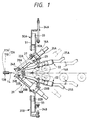
- According to the present embodiment as shown in Fig. 1, there is provided a film peeling device 10 in which two laminated
thin films photoresist layer 11A and a light transmissive resin film 11B are respectively coated on the front and back surfaces of acircuit board 14 to advance along apass line 14A. A pair of front andback vibrators back rods circuit board 14 in such a manner that they surround the circuit board from the front and back surfaces of thecircuit board 14 respectively. The leading ends of the front andback rods circuit board 14 between them. The peeling device 10 includes film floating means 20 which applies the vibratory motions of the front andback rods thin films photoresist layer 11A, and film peeling means 22 for peeling the thus floated portion of the light transmissive resin film 11B. Also, according to the present film peeling device 10, the positions of the leading ends of the front andback rods circuit board 14 are arranged to offset each other along the surface of thecircuit board 14 in a direction of the width of thecircuit board 14 and perpendicular to the advancing direction of thecircuit board 14. - A back back-up
roller 24B and a front back-uproller 24A are disposed at positions opposed to the leading ends of the front andback rods circuit board 14 and two laminatedthin films circuit board 14 and laminatedthin films back rods roller 24A is supported by asupport member 26A of thefront vibrator 16A and the back back-uproller 24B is supported by asupport member 26B of theback vibrator 16B, respectively. The front and back back-uprollers circuit board 14. - Two film peeling means 22 are disposed respectively up and down in Fig. 1 in a manner to correspond to the front and
back vibrators air nozzles support members rollers pass line 14A of thecircuit board 14.Air hoses air nozzles - The front and back back-up
rollers support members support frames elongated holes 29 extending in parallel to the axes of therods elongated holes 29 withbolts 27 provided in therod support members - The
rod support members linear ways linear ways horizontal bars movable members 33 thereof are respectively supported slidably with respect to the fixed-side members 31 in such a manner that they are energized upwardly bysprings - The
horizontal bars pass line 14A and in parallel to the leading end of thecircuit board 14. The two ends of thehorizontal bars side walls 35 of the device and thus, as shown in Figs. 2 and 3, thehorizontal bars lower racks - The upper and
lower racks pinion 38 disposed at a position level with thepass line 14A, so that they can be moved vertically in a direction to approach and to move away from thepass line 14A in synchronization with each other. More specifically, anair cylinder 40 is connected to theupper rack 36A and, by driving theupper rack 36A with theair cylinder 40 through the upperhorizontal bar 32A, thelower rack 36B can be driven through thepinion 38 in synchronization withupper rack 36A. Theupper rack 36A,lower rack 36B,pinion 38, andair cylinder 40 are respectively disposed at the two ends of the upper and lowerhorizontal bars horizontal bars - Additionally, a pair of right and left
front vibrators 16A, a pair of right and left backvibrators 16B, a pair of right and left front back-uprollers 24A, and a pair of right and left back back-uprollers 24B are provided for each of thehorizontal bars air nozzles 22A and twoair nozzles 22B are mounted on each of the vibrators. Therefore, according to the structure of the present embodiment, one back-up roller and two air nozzles can be moved integrally with one vibrator. - In Figs. 2 and 3,
reference characters horizontal bars guide rods movable block 42 through fixedblocks lower racks pinion 38, and guiderods pass line 14A along aguide rail 46A provided on the outside of theside wall 35 and aguide rail 46B provided in part of theside wall 35. Additionally, in theupper guide rail 46A, there is provided a secondmovable block 48 in such a manner that it is movable in parallel with thepass line 14A similarly to themovable block 42. - The lower end of the second
movable block 48 is in mesh with apinion 50A operable in linking with afeed roller 50 for feeding thecircuit board 14 and is connected to a horizontally extendingrack 52 to be driven by thepinion 50A, whereby the secondmovable block 48 can be advanced in synchronization with thecircuit board 14 to be fed by thefeed roller 50. In the secondmovable block 48, there is provided anair cylinder 54 including arod 54A which is connected with themovable block 42. Theair cylinder 54 allows themovable block 42 to move along thepass line 14A in a given range with respect to the secondmovable block 48. A relative position between themovable block 42 and secondmovable block 48 can be controlled by controlling theair cylinder 54 by means of acontrol device 56 shown in Fig. 3. Arod 58A of asecond air cylinder 58 mounted on the side of theside wall 44 is connected to the secondmovable block 48. Thus, the secondmovable block 48 can be reciprocated together with therack 52 along thepass line 14A by thesecond air cylinder 58. Therefore, thecircuit board 14 is driven in synchronization with the secondmovable block 48 by thesecond air cylinder 58 through therack 52 andpinion 50A. - After a circuit board is fed out on completion of a film peeling operation, the
rack 52 and secondmovable block 48 are returned by thesecond air cylinder 58 to their wait positions where they wait for a next circuit board. In this operation, a one-way bearing (not shown) is fitted into thepinion 50A to thereby prevent reversal of thefeed roller 50. - Upper and lower second
horizontal bars movable block 42 integrally therewith. The secondhorizontal bars horizontal bars pass line 14 direction. As shown in Figs. 2 and 4, thin film leadingend sensors end sensors 64 are respectively supported by themovable block 42 throughair cylinders peel film sensors back rods pass line 14A direction sequentially in the order of the thin film leadingend sensors end sensors 64, andpeel film sensors - As shown in Fig. 5, the thin film leading
end sensors conductive contacts circuit board 14. That is, when theconductive contacts end sensors control device 56. - The circuit board leading
end sensors 64 are optical sensors which detect the leading end of thecircuit board 14 when light between thesensors 64 is shielded by the leading end of thecircuit board 14 and thereafter outputs a detect signal to thecontrol device 56. Thepeel film sensors end sensors pass line 14A by theair cylinders pass line 14A by theair cylinders - Next, description will be given below of the operation of the above-mentioned device according to the invention.
- At first, with the second
movable block 48 positioned and fixed at its wait position by thesecond air cylinder 58 as a standard, themovable block 42 is moved and positioned in a pass line direction shown in Fig. 4 by theair cylinder 54. Also, the thin film leadingend sensors circuit board 14. In this state, thecircuit board 14 with the laminatedthin films pass line 14A by the feed roller in the direction of the sensors, film floating means 20, and film peeling means 22. - When the leading end of the circuit-
board 14, as shown in Fig. 6 (C), enters between the upper and lower conductive contacts, opens them, and then reaches a circuit board leading end detect line designated by 65 in Fig. 4, this is detected by the circuit board leadingend sensors 64. Responsive to the detection, theconductive contacts end sensors circuit board 14. Next, the laminatedthin films conductive contacts end sensors conductive contacts control device 56 determines that the thin film leadingend sensors thin films circuit board 14. The secondmovable block 48 is pulled by theair cylinder 58, whereby thecircuit board 14 is advanced in synchronization with the secondmovable block 48 by thepinion 50A through therack 52. Then, the upper and lowerhorizontal bars air cylinder 40 through theracks back vibrators back rod rollers air nozzles - Just as the
circuit board 14 advances and both of the upper and lower thin film leadingend sensors second air cylinder 58,air cylinder 40 andvibrators air cylinder 54 as well. At the same time, air pressure is jetted out from theair nozzles air cylinders end sensors 62A, 2B against thecircuit board 14, is removed and thus thesesensors circuit board 14. - When the
movable block 42 and secondmovable block 48 start to move horizontally, thevibrators back rods circuit board 14. Then, themovable block 42 is driven so as to narrow the distance between the secondmovable block 48. - In the above process, the
air cylinder 54 pulls themovable block 42 by a set distance. Therefore, while the leading ends of the front andback rods thin films circuit board 14, and are also beating the laminatedthin films back rods circuit board 14. If the stroke of the front andback rods thin films circuit board 14 can be absorbed. This makes it possible for the rods to beat assuredly the leading ends of the laminated thin films. - When the leading ends of the laminated
thin films back rods thin films air nozzles circuit board 14 starting at the peeled portions by a film feed device (not shown), and are discharged out externally of the pass line. - In this operation, although the front and
back rods circuit board 14, the back-uprollers back rods circuit board 14 and, therefore, even if the rods beat thecircuit board 14 simultaneously from the front and back sides thereof, there is no possibility that thecircuit board 14 can be distorted. - Also, when the front and
back rods circuit board 14 by theair cylinder 54 through themovable block 42, there is no possibility that the front andback rods circuit board 14 and, therefore, the rods are prevented from being damaged due to their idle beating. - Further, since the back and front back-up
rollers back rods circuit board 14 and laminatedthin films - After the light transmissive resin film 11B is peeled, the
circuit board 14 is caused to pass through the position of the secondmovable block 48, and is then discharged out of the device. Themovable block 42, secondmovable block 48, andrack 52 are then returned to their respective wait positions by theair cylinder 58. This process is then repeated to thereby peel more films. - As described above, in the above-mentioned embodiment, the back-up
rollers circuit board 14 by the leading ends of therods - Additionally, the back-up
rollers vibrator support members - The particular structure shown in Figs. 1-3 for performing the functions of film floating, film peeling, and rod moving represent exemplary cases only and are not to be construed in a limiting fashion. It will be appreciated that any association of elements capable of accomplishing film floating, film peeling, or rod moving would work acceptably in the inventive combination, and Applicant intends that, in its broadest aspects, the present invention is to be limited to that specific structure which is capable of film floating, film peeling, or rod moving.
- Although the invention has been described with reference to a specific embodiment, this description is not meant to be construed in a limiting sense. Various modifications of the disclosed embodiment, as well as other embodiments of the present invention, will become apparent to persons skilled in the art upon reference to the description of the invention. It is therefore contemplated that the appended claims will cover any such modifications or embodiments as fall within the true scope of the invention.
Claims (10)
- A film peeling method in which two laminated thin films (12A, 12B) each consisting of a photoresist layer (11A) and a light transmissive film (11B) are respectively coated on one side and on the opposite side to said one side surface of a circuit board (14), two vibrators (16A, 16B) each including a rod (18A, 18B) are respectively disposed close to each of said sides of the circuit board (14) in such a manner that they surround the circuit board (14) from said one side and said opposite side surfaces of the circuit board (14) respectively as well as leading ends of the rods (18A, 18B) on one side and on the opposite side are disposed to face each other with the circuit board (14) between them, the vibratory motions of the rods (18A, 18B) are applied onto the end portions of the respective laminated thin films (12A, 12B) coated on said one side and said opposite side surfaces of the circuit board (14) to thereby float part of the light transmissive films (11B) from the associated photoresist layers (11A) and the films are peeled off from the floated portions of the light transmissive films (11B), characterized by the steps of:setting the positions of the rod (18A, 18B) leading ends with respect to said circuit board (14) so as to offset each other along the surfaces of said circuit board (14) in a direction of the width of the circuit board (14) and perpendicular to the advancing direction of the circuit board (14);disposing backup members (24A, 24B) on said one side and on said opposite side in such positions as to be respectively opposed to the rods (18A, 18B) leading ends through said circuit board (14) and said laminated thin films (12A, 12B), andmoving said backup members along said circuit board (14) and said two laminated thin films (12A, 12B) respectively in synchronization with said rods (18A, 18B) leading ends.
- A film peeling method as set forth in claim 1,wherein the starting points of application of said vibratory motions to said laminated thin films (12A, 12B) by said rod (18A, 18B) leading ends are respectively set as the end portions of said laminated thin films (12A, 12B) on said one side and said opposite side surfaces of said circuit board (14) further distant from the end edge of an adjoining circuit board (14); andwherein said rod (18A, 18B) leading ends as well as said backup members (24A, 24B) are moved by a given distance from said starting points while said vibratory motions are being applied to said laminated thin films (12A, 12B).
- A film peeling method as set forth in claim 1 or 2,wherein said backup members (24A, 24B) are rollers which are in rollable contact with said laminated thin films (12A, 12B) in the direction of the movements of said rods (18A, 18B).
- A film peeling device for peeling two laminated thin films (12A, 12B), each consisting of a photoresist layer (11A) and a light transmissive film (11B) respectively coated on one side and on the opposite side to said on side surface of a circuit board (14), comprising:two vibrators (16A, 16B), each including a rod (18A, 18B) respectively disposed close to each of said sides of said circuit board (14) in such a manner that they surround the circuit board (14) from said one side and said opposite side surfaces of said circuit board (14) respectively;wherein the positions of said rods (18A, 18B) leading ends are disposed to face each other with the circuit board (14) between them:a film floating means (20) for applying vibratory motions of the rods (18A, 18B) onto the end portions of the laminated thin films (12A, 12B) respectively coated on said one side and said opposite side surfaces of the circuit board (14) to thereby float part of the light transmissive films (11B) from their respective photoresist layers (11A); anda film peeling means (22) for peeling the films in the floated portions of the light transmissive films (11B);
characterized in thatsaid rod leading means are set so as to offset each other in respect to the surfaces of said circuit board (14); andthat the peeling device comprises backup members (24A, 24B) respectively provided at positions opposed to said rods (18A, 18B) leading ends through said circuit board (14) and said laminated thin films (12A, 12B) and movable in contact with and along said circuit board (14) and said laminated thin films (12A, 12B) in synchronization with said opposed rods (18A, 18B) leading ends; - A film peeling device as set forth in claim 4, wherein said backup members (24A, 24B) are respectively supported by support members (26A, 26B) of said vibrators (16A, 16B).
- A thin film peeling device as set forth in claim 4 or 5, wherein said backup members (24A, 24B) are respectively formed of hard rubber.
- A film peeling device as set forth in one of the claims 4, 5 or 6, wherein said backup members (24A, 24B) are respectively rollers.
- A film peeling device as set forth in one of the claims 4, 5, 6 or 7, wherein said film floating means (20) includes rod moving means for moving said rods (18A, 18B) leading ends relatively in the advancing direction of said circuit board (14).
- A film peeling device as set forth in claim 8, wherein said film floating means (20) includes:film leading end sensors (62A, 62B) respectively for detecting the leading ends of said laminated thin films (12A, 12B) on said one side and said opposite side in the advancing direction of said circuit board (14); anda control device for detecting the leading end of the laminated thin film (12A, 12B) extending from the leading end of said circuit board (14) in the advancing direction in accordance with output signals from said film leading end sensors (62A, 62B) and for controlling said rod moving means to position said rods (18A, 18B) leading ends at said detected leading end, and for moving them by a given distance from said position in said circuit board (14) advancing direction.
- A film peeling device as set forth in claim 9, wherein said laminated thin film sensors each includes a pair of conductive contacts (68A, 68B) disposed spaced apart from each other, in the width direction of said circuit board (14) and contactable with the surfaces of said circuit board (14) and said laminated thin films (12A, 12B) respectively coated on said circuit board (14) and also wherein said laminated thin film sensors run over said laminated thin films (12A, 12B) when said pair of conductive contacts (68A, 68B) come into contact with conductive layers respectively provided on said surfaces of said circuit board (14) and outputs a thin film detect signal when the conduction is cut off.
Applications Claiming Priority (3)
| Application Number | Priority Date | Filing Date | Title |
|---|---|---|---|
| JP124093/94 | 1994-06-06 | ||
| JP12409394 | 1994-06-06 | ||
| JP6124093A JP2644184B2 (en) | 1994-06-06 | 1994-06-06 | Film peeling method and apparatus |
Publications (3)
| Publication Number | Publication Date |
|---|---|
| EP0686477A2 EP0686477A2 (en) | 1995-12-13 |
| EP0686477A3 EP0686477A3 (en) | 1996-05-01 |
| EP0686477B1 true EP0686477B1 (en) | 2000-01-26 |
Family
ID=14876755
Family Applications (1)
| Application Number | Title | Priority Date | Filing Date |
|---|---|---|---|
| EP94116993A Expired - Lifetime EP0686477B1 (en) | 1994-06-06 | 1994-10-27 | Method and device for peeling a film |
Country Status (9)
| Country | Link |
|---|---|
| US (1) | US5496432A (en) |
| EP (1) | EP0686477B1 (en) |
| JP (1) | JP2644184B2 (en) |
| KR (1) | KR100226378B1 (en) |
| CN (1) | CN1039076C (en) |
| DE (1) | DE69422802T2 (en) |
| HK (1) | HK1012306A1 (en) |
| MY (1) | MY114168A (en) |
| TW (1) | TW315579B (en) |
Families Citing this family (17)
| Publication number | Priority date | Publication date | Assignee | Title |
|---|---|---|---|---|
| US6445969B1 (en) * | 1997-01-27 | 2002-09-03 | Circuit Image Systems | Statistical process control integration systems and methods for monitoring manufacturing processes |
| US6022445A (en) * | 1997-05-06 | 2000-02-08 | Tissue Engineering, Inc. | Method and apparatus for removal of biopolymer constructs from support structures |
| US5937497A (en) * | 1997-12-29 | 1999-08-17 | Micron Electronics, Inc. | Method for removing parts from tape |
| US6009686A (en) * | 1997-12-29 | 2000-01-04 | Micron Electronics, Inc. | De-reeler for tape holding parts |
| US6502783B1 (en) | 2000-08-15 | 2003-01-07 | Micron Technology, Inc. | Carrier tape recycling apparatus and method of recycling carrier tape |
| US6524881B1 (en) * | 2000-08-25 | 2003-02-25 | Micron Technology, Inc. | Method and apparatus for marking a bare semiconductor die |
| US7169685B2 (en) | 2002-02-25 | 2007-01-30 | Micron Technology, Inc. | Wafer back side coating to balance stress from passivation layer on front of wafer and be used as die attach adhesive |
| TWI341788B (en) * | 2004-07-06 | 2011-05-11 | Fujifilm Corp | Apparatus for and method of manufacturing photosensitive laminated body |
| JP4445457B2 (en) * | 2005-11-11 | 2010-04-07 | 株式会社アドテックエンジニアリング | Film peeling device |
| KR100771338B1 (en) * | 2006-08-28 | 2007-10-29 | 삼성전기주식회사 | Peeling apparatus of protectin sheets for printed circuit board |
| KR100751712B1 (en) * | 2007-01-31 | 2007-08-23 | 최병수 | Apparatus for separating protected film from printed circuit board |
| CN101398864B (en) * | 2007-09-28 | 2011-12-21 | 富葵精密组件(深圳)有限公司 | Circuit board making and emulating system and method |
| CN102059842B (en) * | 2009-11-12 | 2013-04-17 | 南亚电路板股份有限公司 | Separation device and separation method thereof |
| JP6062210B2 (en) * | 2012-10-31 | 2017-01-18 | 株式会社日立プラントメカニクス | Film peeling device |
| TWI650241B (en) | 2017-11-30 | 2019-02-11 | 景碩科技股份有限公司 | Tear film mechanism |
| TWI714890B (en) * | 2018-09-28 | 2021-01-01 | 景碩科技股份有限公司 | Peeling device |
| CN112078874B (en) * | 2020-09-02 | 2021-10-01 | 饶明明 | Packing apparatus is used in production of electric motorcycle car accessory |
Family Cites Families (5)
| Publication number | Priority date | Publication date | Assignee | Title |
|---|---|---|---|---|
| JPS62293246A (en) * | 1986-06-13 | 1987-12-19 | Asahi Chem Ind Co Ltd | Method and apparatus for peeling cover film |
| DE69023327T2 (en) * | 1990-04-06 | 1996-06-13 | Somar Corp | Transfer development method and device for carrying it out. |
| JP2531169Y2 (en) * | 1991-11-25 | 1997-04-02 | 住友電気工業株式会社 | Stripping equipment for coated wire |
| DE4221703C2 (en) * | 1992-07-02 | 1996-02-22 | Emco Maier Gmbh | Method and device for removing protective films on one or both sides |
| JPH06329329A (en) * | 1993-05-18 | 1994-11-29 | Adtec Eng:Kk | Film separating device |
-
1994
- 1994-06-06 JP JP6124093A patent/JP2644184B2/en not_active Expired - Fee Related
- 1994-08-24 TW TW083107761A patent/TW315579B/zh active
- 1994-10-21 US US08/327,384 patent/US5496432A/en not_active Expired - Fee Related
- 1994-10-27 EP EP94116993A patent/EP0686477B1/en not_active Expired - Lifetime
- 1994-10-27 DE DE69422802T patent/DE69422802T2/en not_active Expired - Fee Related
-
1995
- 1995-05-03 MY MYPI95001163A patent/MY114168A/en unknown
- 1995-05-12 KR KR1019950011663A patent/KR100226378B1/en not_active IP Right Cessation
- 1995-05-15 CN CN95106505A patent/CN1039076C/en not_active Expired - Fee Related
-
1998
- 1998-12-15 HK HK98113431A patent/HK1012306A1/en not_active IP Right Cessation
Also Published As
| Publication number | Publication date |
|---|---|
| TW315579B (en) | 1997-09-11 |
| DE69422802T2 (en) | 2000-06-21 |
| HK1012306A1 (en) | 1999-07-30 |
| CN1115958A (en) | 1996-01-31 |
| CN1039076C (en) | 1998-07-08 |
| EP0686477A2 (en) | 1995-12-13 |
| JPH07330213A (en) | 1995-12-19 |
| KR960003517A (en) | 1996-01-26 |
| DE69422802D1 (en) | 2000-03-02 |
| EP0686477A3 (en) | 1996-05-01 |
| JP2644184B2 (en) | 1997-08-25 |
| KR100226378B1 (en) | 1999-10-15 |
| US5496432A (en) | 1996-03-05 |
| MY114168A (en) | 2002-08-30 |
Similar Documents
| Publication | Publication Date | Title |
|---|---|---|
| EP0686477B1 (en) | Method and device for peeling a film | |
| EP0744286B1 (en) | Film applying method and apparatus for carrying out the same | |
| US4921566A (en) | Apparatus for the laminating and cutting of photoresist webs | |
| CA2014648A1 (en) | Apparatus and method for single side spray processing of printed circuit boards | |
| DK0992352T3 (en) | Method and apparatus for printing on continuously passed material web / sheets | |
| US4961817A (en) | Thin-film releasing apparatus | |
| US5454247A (en) | Method of and apparatus for punching and bending a lithographic plate | |
| WO1994029043A1 (en) | Method, apparatus for punching and bending plate | |
| EP0215397B1 (en) | Film peeling apparatus | |
| JPH07112298A (en) | Automatic working method of both ends of long size work and device therefor | |
| EP0229842A1 (en) | Laminator | |
| CA1292409C (en) | Thin-film coating method and apparatus therefor | |
| US4307961A (en) | Apparatus for precisely aligning a pair of elements | |
| JPH0831710B2 (en) | Substrate transfer device | |
| US4966647A (en) | Method for single side spray processing of printed circuit boards | |
| KR0121440Y1 (en) | Automatic press device for the manufacture of flexible print board | |
| US4650390A (en) | Stacker-loader for stacking double sided printed circuit boards | |
| JP3287219B2 (en) | Film peeling method and apparatus | |
| JP2897073B2 (en) | Plate-like reversing device | |
| JPH05177582A (en) | Method and device for cutting board | |
| JP2772779B2 (en) | Panel nailing device | |
| JPH0722724B2 (en) | Spray equipment | |
| JP3390856B2 (en) | Film peeling device | |
| JPH01145144A (en) | Automatic printing press for applying liquid photoresist | |
| JP4110225B2 (en) | Manufacturing method and apparatus of inorganic board |
Legal Events
| Date | Code | Title | Description |
|---|---|---|---|
| PUAI | Public reference made under article 153(3) epc to a published international application that has entered the european phase |
Free format text: ORIGINAL CODE: 0009012 |
|
| AK | Designated contracting states |
Kind code of ref document: A2 Designated state(s): DE GB |
|
| PUAL | Search report despatched |
Free format text: ORIGINAL CODE: 0009013 |
|
| AK | Designated contracting states |
Kind code of ref document: A3 Designated state(s): DE GB |
|
| 17P | Request for examination filed |
Effective date: 19960819 |
|
| 17Q | First examination report despatched |
Effective date: 19980518 |
|
| GRAG | Despatch of communication of intention to grant |
Free format text: ORIGINAL CODE: EPIDOS AGRA |
|
| GRAG | Despatch of communication of intention to grant |
Free format text: ORIGINAL CODE: EPIDOS AGRA |
|
| GRAH | Despatch of communication of intention to grant a patent |
Free format text: ORIGINAL CODE: EPIDOS IGRA |
|
| GRAH | Despatch of communication of intention to grant a patent |
Free format text: ORIGINAL CODE: EPIDOS IGRA |
|
| GRAA | (expected) grant |
Free format text: ORIGINAL CODE: 0009210 |
|
| AK | Designated contracting states |
Kind code of ref document: B1 Designated state(s): DE GB |
|
| REF | Corresponds to: |
Ref document number: 69422802 Country of ref document: DE Date of ref document: 20000302 |
|
| PLBE | No opposition filed within time limit |
Free format text: ORIGINAL CODE: 0009261 |
|
| STAA | Information on the status of an ep patent application or granted ep patent |
Free format text: STATUS: NO OPPOSITION FILED WITHIN TIME LIMIT |
|
| 26N | No opposition filed | ||
| REG | Reference to a national code |
Ref country code: GB Ref legal event code: IF02 |
|
| PGFP | Annual fee paid to national office [announced via postgrant information from national office to epo] |
Ref country code: DE Payment date: 20021031 Year of fee payment: 9 |
|
| PGFP | Annual fee paid to national office [announced via postgrant information from national office to epo] |
Ref country code: GB Payment date: 20030319 Year of fee payment: 9 |
|
| PG25 | Lapsed in a contracting state [announced via postgrant information from national office to epo] |
Ref country code: GB Free format text: LAPSE BECAUSE OF NON-PAYMENT OF DUE FEES Effective date: 20031027 |
|
| PG25 | Lapsed in a contracting state [announced via postgrant information from national office to epo] |
Ref country code: DE Free format text: LAPSE BECAUSE OF NON-PAYMENT OF DUE FEES Effective date: 20040501 |
|
| GBPC | Gb: european patent ceased through non-payment of renewal fee |
Effective date: 20031027 |