EP0690493A2 - Shallow trench isolation with thin nitride liner - Google Patents
Shallow trench isolation with thin nitride liner Download PDFInfo
- Publication number
- EP0690493A2 EP0690493A2 EP95480072A EP95480072A EP0690493A2 EP 0690493 A2 EP0690493 A2 EP 0690493A2 EP 95480072 A EP95480072 A EP 95480072A EP 95480072 A EP95480072 A EP 95480072A EP 0690493 A2 EP0690493 A2 EP 0690493A2
- Authority
- EP
- European Patent Office
- Prior art keywords
- layer
- oxide
- nitride
- trench
- filling
- Prior art date
- Legal status (The legal status is an assumption and is not a legal conclusion. Google has not performed a legal analysis and makes no representation as to the accuracy of the status listed.)
- Granted
Links
Images
Classifications
-
- H—ELECTRICITY
- H01—ELECTRIC ELEMENTS
- H01L—SEMICONDUCTOR DEVICES NOT COVERED BY CLASS H10
- H01L21/00—Processes or apparatus adapted for the manufacture or treatment of semiconductor or solid state devices or of parts thereof
- H01L21/02—Manufacture or treatment of semiconductor devices or of parts thereof
- H01L21/04—Manufacture or treatment of semiconductor devices or of parts thereof the devices having at least one potential-jump barrier or surface barrier, e.g. PN junction, depletion layer or carrier concentration layer
- H01L21/18—Manufacture or treatment of semiconductor devices or of parts thereof the devices having at least one potential-jump barrier or surface barrier, e.g. PN junction, depletion layer or carrier concentration layer the devices having semiconductor bodies comprising elements of Group IV of the Periodic System or AIIIBV compounds with or without impurities, e.g. doping materials
- H01L21/30—Treatment of semiconductor bodies using processes or apparatus not provided for in groups H01L21/20 - H01L21/26
- H01L21/31—Treatment of semiconductor bodies using processes or apparatus not provided for in groups H01L21/20 - H01L21/26 to form insulating layers thereon, e.g. for masking or by using photolithographic techniques; After treatment of these layers; Selection of materials for these layers
- H01L21/3105—After-treatment
-
- H—ELECTRICITY
- H01—ELECTRIC ELEMENTS
- H01L—SEMICONDUCTOR DEVICES NOT COVERED BY CLASS H10
- H01L21/00—Processes or apparatus adapted for the manufacture or treatment of semiconductor or solid state devices or of parts thereof
- H01L21/70—Manufacture or treatment of devices consisting of a plurality of solid state components formed in or on a common substrate or of parts thereof; Manufacture of integrated circuit devices or of parts thereof
- H01L21/71—Manufacture of specific parts of devices defined in group H01L21/70
- H01L21/76—Making of isolation regions between components
- H01L21/762—Dielectric regions, e.g. EPIC dielectric isolation, LOCOS; Trench refilling techniques, SOI technology, use of channel stoppers
- H01L21/76224—Dielectric regions, e.g. EPIC dielectric isolation, LOCOS; Trench refilling techniques, SOI technology, use of channel stoppers using trench refilling with dielectric materials
- H01L21/76232—Dielectric regions, e.g. EPIC dielectric isolation, LOCOS; Trench refilling techniques, SOI technology, use of channel stoppers using trench refilling with dielectric materials of trenches having a shape other than rectangular or V-shape, e.g. rounded corners, oblique or rounded trench walls
-
- Y—GENERAL TAGGING OF NEW TECHNOLOGICAL DEVELOPMENTS; GENERAL TAGGING OF CROSS-SECTIONAL TECHNOLOGIES SPANNING OVER SEVERAL SECTIONS OF THE IPC; TECHNICAL SUBJECTS COVERED BY FORMER USPC CROSS-REFERENCE ART COLLECTIONS [XRACs] AND DIGESTS
- Y10—TECHNICAL SUBJECTS COVERED BY FORMER USPC
- Y10S—TECHNICAL SUBJECTS COVERED BY FORMER USPC CROSS-REFERENCE ART COLLECTIONS [XRACs] AND DIGESTS
- Y10S148/00—Metal treatment
- Y10S148/05—Etch and refill
Definitions
- the field of the invention is that of trench isolation integrated circuit processing, including a dielectric layer on the interior of the trench.
- US-A- 4 631 803 illustrates a set of different liners that are used to relief the stress.
- One example is an oxide-nitride (ON) layer
- another example is a triple layer of oxide-nitride-oxide (ONO).
- This and other references illustrate a rather thick layer of oxide in the range of 20-45 nm and a relatively thick layer of nitride in the range of 30-60 nm.
- Another article "Oxidation-Induced Defect Generation in Advanced DRAM Structures" by S. R. Stiffler, et al. in IEEE Transactions on Electron Devices, Vol. 37, No. 5, May 1990 illustrates a relatively thin layer of nitride of thickness 7 nm.
- a problem with this and other nitride liners in the art is that when a conventional stripping process of hot phosphoric acid is used to strip the protective pad nitride that coats the wafer, the phosphoric acid recesses the nitride liner, exposing a gap. Subsequent etches in hydrofluoric acid cause that recess to expand into an unacceptably large void.
- the invention relates to a process for forming an isolating trench in which the trench is etched in a reactive ion etching process, and lined with a thin liner of nitride having a thickness ⁇ 5 nm.
- a feature of the invention is the use of a pyrogenic oxide anneal (wet oxidation) at a temperature of about 800°C. This anneal densifies the oxide liner as is conventional, but at a much lower temperature than conventional argon annealing.
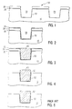
- Fig. 1 illustrates in cross-section a portion of a trench according to the invention.
- Figs. 2 to 4 illustrate the trench in subsequent stages of fabrication.
- Fig. 5 illustrates in cross-section a prior art trench at the final stage of fabrication.
- a conventional reactive ion etching process (CF4 - CHF3 - Ar) has cut through the oxide and nitride and cut isolation trenches 50 to an illustrative depth of about 0.1 - 1 ⁇ m.
- a thermal oxidation step has produced a thin layer 52, shown as a thick line in the drawing, of thermal oxide (SiO2) having a nominal thickness of about 20nm to stabilize the surface.
- top and bottom corners of the trench are susceptible to crystal defects caused by stress produced by the oxidation process.
- the art has tried a number of methods to relieve the stress, including forming layers of nitride (Si3N4) and/or oxide.
- a problem that has been encountered in the prior art is that when pad nitride 30 is stripped in a conventional stripping process using hot phosphoric acid, the phosphoric acid penetrates down along the nitride trench liner and produces a recess. Such a problem is illustrated with respect to Fig. 5 showing a recess 32' that is unacceptable because it exposes the oxide filler 60 in the trench and the oxide liner 52 to attack in subsequent etching steps. Whenever a conventional dip in hydrofluoric acid is used, the recess 32' will be expanded, producing ultimately an unacceptably large void in the trench fill.
- Fig. 2 illustrates the results of a step according to the invention of depositing a layer of 4nm of LPCVD nitride at a pressure of 200 mTorr with a flow of NH3:SiH2Cl2 10:1 for 2 minutes at 770°C.
- a preferred embodiment employs a lower deposition temperature, such as 720°C, in order to provide better control of nitride liner thickness.
- a layer has been discovered to be immune to the recessing problem discussed above.
- Fig. 3 there is shown an oxide liner 60 after deposition of 550nm of TEOS (tetra-ethyl-orthosilicate) oxide and a step of annealing and densifying the oxide.
- the densification step is conducted as a pyrogenic oxidation anneal (wet oxidation, meaning an anneal during oxidation conditions) at a temperature of 800°C. At this temperature, the result of the wet oxidation anneal is comparable in densification of the oxide liner 60 to the results of a conventional annealing step in argon ambient at 1000°C.
- the etch resistance in hydrofluoric acid is also the same as oxide annealed in argon.
- an additional benefit of the invention is that the oxidizing ambient can be effective in driving out unwanted impurities from the dielectric.
- a convenient trench fill process is an ozone assisted TEOS process as disclosed in K. Fujino, et al J. Electrochemical Soc. Vol 137, p. 2883, 1990, in the course of which sizable amounts of fluorine are mixed in with the oxide.
- the wet oxidation step readily removes the fluorine, which is not the case with an argon anneal.
- Fig. 4 the same trench 50 is shown after the stripping process for the pad nitride and pad oxide.
- the nitride liner 32 is shown as flush with the substrate surface. It has been observed that, although the 7 nm liner had an etch rate of 10 nm per minute in a conventional hot phosphoric acid bath at 165°C, the 4 nm illustrative layer withstood a nominal 25 minute overetch with no detectable recessing.
Abstract


Description
- The field of the invention is that of trench isolation integrated circuit processing, including a dielectric layer on the interior of the trench.
- In trench isolated integrate circuits, a known problem has been that of stress caused by the dielectric fill in the trench on the silicon substrate. US-A- 4 631 803 illustrates a set of different liners that are used to relief the stress. One example is an oxide-nitride (ON) layer, another example is a triple layer of oxide-nitride-oxide (ONO). This and other references illustrate a rather thick layer of oxide in the range of 20-45 nm and a relatively thick layer of nitride in the range of 30-60 nm. Another article "Oxidation-Induced Defect Generation in Advanced DRAM Structures" by S. R. Stiffler, et al. in IEEE Transactions on Electron Devices, Vol. 37, No. 5, May 1990 illustrates a relatively thin layer of nitride of thickness 7 nm.
- A problem with this and other nitride liners in the art is that when a conventional stripping process of hot phosphoric acid is used to strip the protective pad nitride that coats the wafer, the phosphoric acid recesses the nitride liner, exposing a gap. Subsequent etches in hydrofluoric acid cause that recess to expand into an unacceptably large void.
- The invention relates to a process for forming an isolating trench in which the trench is etched in a reactive ion etching process, and lined with a thin liner of nitride having a thickness < 5 nm.
- A feature of the invention is the use of a pyrogenic oxide anneal (wet oxidation) at a temperature of about 800°C. This anneal densifies the oxide liner as is conventional, but at a much lower temperature than conventional argon annealing.
- Fig. 1 illustrates in cross-section a portion of a trench according to the invention.
- Figs. 2 to 4 illustrate the trench in subsequent stages of fabrication.
- Fig. 5 illustrates in cross-section a prior art trench at the final stage of fabrication.
- Referring now to Fig. 1, there is shown a portion of an substrate (or epitaxial layer) 10 having a conventional pad oxide liner 20 of thickness about 8nm and a conventional
pad nitride layer 30 of thickness about 150nm. A conventional reactive ion etching process (CF₄ - CHF₃ - Ar) has cut through the oxide and nitride and cutisolation trenches 50 to an illustrative depth of about 0.1 - 1µm. A thermal oxidation step has produced athin layer 52, shown as a thick line in the drawing, of thermal oxide (SiO₂) having a nominal thickness of about 20nm to stabilize the surface. Those skilled in the art are well aware that the top and bottom corners of the trench are susceptible to crystal defects caused by stress produced by the oxidation process. The art has tried a number of methods to relieve the stress, including forming layers of nitride (Si₃N₄) and/or oxide. - A problem that has been encountered in the prior art is that when
pad nitride 30 is stripped in a conventional stripping process using hot phosphoric acid, the phosphoric acid penetrates down along the nitride trench liner and produces a recess. Such a problem is illustrated with respect to Fig. 5 showing a recess 32' that is unacceptable because it exposes theoxide filler 60 in the trench and theoxide liner 52 to attack in subsequent etching steps. Whenever a conventional dip in hydrofluoric acid is used, the recess 32' will be expanded, producing ultimately an unacceptably large void in the trench fill. - Fig. 2 illustrates the results of a step according to the invention of depositing a layer of 4nm of LPCVD nitride at a pressure of 200 mTorr with a flow of NH₃:SiH₂Cl₂ 10:1 for 2 minutes at 770°C. Those skilled in the art will readily be able to vary these parameters to suit their circumstances, such as by changing the temperature (less than 800°C), flow rate, etc. A preferred embodiment employs a lower deposition temperature, such as 720°C, in order to provide better control of nitride liner thickness. As will be discussed below, such a layer has been discovered to be immune to the recessing problem discussed above.
- Referring now to Fig. 3, there is shown an
oxide liner 60 after deposition of 550nm of TEOS (tetra-ethyl-orthosilicate) oxide and a step of annealing and densifying the oxide. The densification step is conducted as a pyrogenic oxidation anneal (wet oxidation, meaning an anneal during oxidation conditions) at a temperature of 800°C. At this temperature, the result of the wet oxidation anneal is comparable in densification of theoxide liner 60 to the results of a conventional annealing step in argon ambient at 1000°C. The etch resistance in hydrofluoric acid is also the same as oxide annealed in argon. The use of the lower temperature has the important benefit that the heat load on the substrate is reduced, and thus the diffusion spread of dopants that have previously been implanted or diffused is much reduced. Oxidizing anneals have not been practiced in the art because of the stress caused by oxidizing a filled trench. If the nitride liner is not perfect, oxygen will diffuse down through the trench material and any holes in a liner into the substrate, causing oxidation behind the nitride liner with a consequent increase in stress. An advantageous feature of the invention is that this and other oxidation steps can be repeated with no detectable crystal defect generation in the vicinity of the trench. It has been observed that a nitride liner of thickness 3nm formed under the above conditions did permit oxidation of the substrate behind the liner. - An additional benefit of the invention is that the oxidizing ambient can be effective in driving out unwanted impurities from the dielectric. For example, a convenient trench fill process is an ozone assisted TEOS process as disclosed in K. Fujino, et al J. Electrochemical Soc. Vol 137, p. 2883, 1990, in the course of which sizable amounts of fluorine are mixed in with the oxide. The wet oxidation step readily removes the fluorine, which is not the case with an argon anneal.
- Referring now to Fig. 4, the
same trench 50 is shown after the stripping process for the pad nitride and pad oxide. Thenitride liner 32 is shown as flush with the substrate surface. It has been observed that, although the 7 nm liner had an etch rate of 10 nm per minute in a conventional hot phosphoric acid bath at 165°C, the 4 nm illustrative layer withstood a nominal 25 minute overetch with no detectable recessing. - As a result of this improvement, the process window for forming shallow trenches and the amount of stress has been considerably increased. Those skilled in the art will readily appreciate that a number of parameters may be varied while still keeping within the concept of the invention and the following claims are not meant to be limited to the embodiment disclosed.
Claims (9)
- A method of forming isolation members embedded in a silicon layer of an integrated circuit comprising the steps of:
depositing a protective layer containing at least one layer of nitride on a top surface of a silicon layer;
etching through said protective layer to form a set of isolation mask apertures;
etching through said set of isolation mask apertures in a reactive ion etch process to form a set of isolation trenches;
depositing a conformal layer of nitride having a thickness less than 5nm;
depositing a CVD layer of oxide having a thickness sufficient to fill said set of isolation trenches;
removing that portion of said CVD layer of oxide outside said set of isolation trenches to expose said at least one layer of nitride; and
stripping said at least one layer of nitride in phosphoric acid. - A method according to claim 1, in which said step of filling said trench is followed by a step of annealing said CVD layer of oxide in a pyrogenic oxidation anneal.
- A method according to claim 2, in which said step of filling said trench comprises ozone-assisted deposition of TEOS and in which said step of annealing said CVD layer of oxide in a pyrogenic oxidation anneal drives out fluorine from said CVD layer of oxide.
- A method according to claim 1, in which said step of filling said trench is conducted at a temperature of less than 800°C.
- A method according to claim 4, in which said step of filling said trench is followed by a step of annealing said CVD layer of oxide in a pyrogenic oxidation anneal.
- A method according to claim 5, in which said step of filling said trench comprises ozone-assisted deposition of TEOS and in which said step of annealing said CVD layer of oxide in a pyrogenic oxidation anneal drives out fluorine from said CVD layer of oxide.
- A method according to claim 1, in which said step of depositing a conformal layer of nitride is preceded by a step of growing a thin layer of thermal oxide.
- A method according to claim 7, in which said step of filling said trench is followed by a step of annealing said CVD layer of oxide in a pyrogenic oxidation anneal.
- A method according to claim 8, in which said step of filling said trench comprises ozone-assisted deposition of TEOS and in which said step of annealing said CVD layer of oxide in a pyrogenic oxidation anneal drives out fluorine from said CVD layer of oxide.
Applications Claiming Priority (2)
| Application Number | Priority Date | Filing Date | Title |
|---|---|---|---|
| US268378 | 1994-06-29 | ||
| US08/268,378 US5447884A (en) | 1994-06-29 | 1994-06-29 | Shallow trench isolation with thin nitride liner |
Publications (3)
| Publication Number | Publication Date |
|---|---|
| EP0690493A2 true EP0690493A2 (en) | 1996-01-03 |
| EP0690493A3 EP0690493A3 (en) | 1996-09-04 |
| EP0690493B1 EP0690493B1 (en) | 1998-08-26 |
Family
ID=23022734
Family Applications (1)
| Application Number | Title | Priority Date | Filing Date |
|---|---|---|---|
| EP95480072A Expired - Lifetime EP0690493B1 (en) | 1994-06-29 | 1995-06-09 | Shallow trench isolation with thin nitride liner |
Country Status (4)
| Country | Link |
|---|---|
| US (1) | US5447884A (en) |
| EP (1) | EP0690493B1 (en) |
| JP (1) | JP3079011B2 (en) |
| DE (1) | DE69504252T2 (en) |
Cited By (4)
| Publication number | Priority date | Publication date | Assignee | Title |
|---|---|---|---|---|
| FR2766012A1 (en) * | 1997-07-08 | 1999-01-15 | France Telecom | PROCESS FOR MINIMIZING THE CORNER EFFECT BY DENSIFICATION OF THE INSULATION LAYER |
| US7247208B2 (en) | 2001-07-09 | 2007-07-24 | Mallinckrodt Baker, Inc. | Microelectronic cleaning compositions containing ammonia-free fluoride salts |
| US8501632B2 (en) | 2005-12-20 | 2013-08-06 | Infineon Technologies Ag | Methods of fabricating isolation regions of semiconductor devices and structures thereof |
| US8936995B2 (en) | 2006-03-01 | 2015-01-20 | Infineon Technologies Ag | Methods of fabricating isolation regions of semiconductor devices and structures thereof |
Families Citing this family (138)
| Publication number | Priority date | Publication date | Assignee | Title |
|---|---|---|---|---|
| US5433794A (en) * | 1992-12-10 | 1995-07-18 | Micron Technology, Inc. | Spacers used to form isolation trenches with improved corners |
| US5652176A (en) * | 1995-02-24 | 1997-07-29 | Motorola, Inc. | Method for providing trench isolation and borderless contact |
| KR0151051B1 (en) * | 1995-05-30 | 1998-12-01 | 김광호 | Method of forming insulation film for semiconductor device |
| US5643823A (en) * | 1995-09-21 | 1997-07-01 | Siemens Aktiengesellschaft | Application of thin crystalline Si3 N4 liners in shallow trench isolation (STI) structures |
| US5985735A (en) * | 1995-09-29 | 1999-11-16 | Intel Corporation | Trench isolation process using nitrogen preconditioning to reduce crystal defects |
| US5811347A (en) * | 1996-04-29 | 1998-09-22 | Advanced Micro Devices, Inc. | Nitrogenated trench liner for improved shallow trench isolation |
| US5706164A (en) * | 1996-07-17 | 1998-01-06 | Vangaurd International Semiconductor Corporation | Method of fabricating high density integrated circuits, containing stacked capacitor DRAM devices, using elevated trench isolation and isolation spacers |
| US5923991A (en) * | 1996-11-05 | 1999-07-13 | International Business Machines Corporation | Methods to prevent divot formation in shallow trench isolation areas |
| US6114741A (en) * | 1996-12-13 | 2000-09-05 | Texas Instruments Incorporated | Trench isolation of a CMOS structure |
| US5763315A (en) * | 1997-01-28 | 1998-06-09 | International Business Machines Corporation | Shallow trench isolation with oxide-nitride/oxynitride liner |
| TW388100B (en) | 1997-02-18 | 2000-04-21 | Hitachi Ulsi Eng Corp | Semiconductor deivce and process for producing the same |
| CN1112727C (en) * | 1997-02-18 | 2003-06-25 | 株式会社日立制作所 | Semiconductor device and process for producing the same |
| US6097076A (en) * | 1997-03-25 | 2000-08-01 | Micron Technology, Inc. | Self-aligned isolation trench |
| JPH10289946A (en) * | 1997-04-14 | 1998-10-27 | Toshiba Corp | Manufacture of semiconductor device |
| US6121552A (en) * | 1997-06-13 | 2000-09-19 | The Regents Of The University Of Caliofornia | Microfabricated high aspect ratio device with an electrical isolation trench |
| US6555484B1 (en) | 1997-06-19 | 2003-04-29 | Cypress Semiconductor Corp. | Method for controlling the oxidation of implanted silicon |
| KR100230425B1 (en) * | 1997-06-20 | 1999-11-15 | 윤종용 | Method for forming trench isolation layer having void |
| KR100444314B1 (en) * | 1997-06-30 | 2004-11-03 | 주식회사 하이닉스반도체 | Method for manufacturing semiconductor device with trench isolation layer without moat |
| US6057209A (en) * | 1997-07-10 | 2000-05-02 | Advanced Micro Devices, Inc. | Semiconductor device having a nitrogen bearing isolation region |
| KR100230431B1 (en) * | 1997-07-25 | 1999-11-15 | 윤종용 | Method of forming trench isolation using two kinds of oxides films |
| US6132631A (en) * | 1997-08-08 | 2000-10-17 | Applied Materials, Inc. | Anisotropic silicon nitride etching for shallow trench isolation in an high density plasma system |
| US6087243A (en) * | 1997-10-21 | 2000-07-11 | Advanced Micro Devices, Inc. | Method of forming trench isolation with high integrity, ultra thin gate oxide |
| KR100446286B1 (en) * | 1997-10-22 | 2004-10-14 | 삼성전자주식회사 | Trench isolation method of semiconductor device for improving uniformity of planarization process |
| KR100244299B1 (en) * | 1997-12-13 | 2000-03-02 | 김영환 | Isolation region of semiconductor device and method forming the same |
| US6008109A (en) * | 1997-12-19 | 1999-12-28 | Advanced Micro Devices, Inc. | Trench isolation structure having a low K dielectric encapsulated by oxide |
| US6140691A (en) * | 1997-12-19 | 2000-10-31 | Advanced Micro Devices, Inc. | Trench isolation structure having a low K dielectric material isolated from a silicon-based substrate |
| US5882983A (en) * | 1997-12-19 | 1999-03-16 | Advanced Micro Devices, Inc. | Trench isolation structure partially bound between a pair of low K dielectric structures |
| US6960818B1 (en) * | 1997-12-30 | 2005-11-01 | Siemens Aktiengesellschaft | Recessed shallow trench isolation structure nitride liner and method for making same |
| US6153478A (en) * | 1998-01-28 | 2000-11-28 | United Microelectronics Corp. | STI process for eliminating kink effect |
| GB9801655D0 (en) * | 1998-01-28 | 1998-03-25 | Trikon Equip Ltd | Method and apparatus for treating a substrate |
| KR100275908B1 (en) * | 1998-03-02 | 2000-12-15 | 윤종용 | Method of fabricating trench isolation in an integrated circuit |
| US6727569B1 (en) | 1998-04-21 | 2004-04-27 | Advanced Micro Devices, Inc. | Method of making enhanced trench oxide with low temperature nitrogen integration |
| TW383451B (en) * | 1998-05-05 | 2000-03-01 | United Microelectronics Corp | Manufacturing method for shallow trench isolation structure |
| KR100280107B1 (en) | 1998-05-07 | 2001-03-02 | 윤종용 | How to form trench isolation |
| EP0959496B1 (en) * | 1998-05-22 | 2006-07-19 | Applied Materials, Inc. | Methods for forming self-planarized dielectric layer for shallow trench isolation |
| US5880006A (en) * | 1998-05-22 | 1999-03-09 | Vlsi Technology, Inc. | Method for fabrication of a semiconductor device |
| US6165869A (en) * | 1998-06-11 | 2000-12-26 | Chartered Semiconductor Manufacturing, Ltd. | Method to avoid dishing in forming trenches for shallow trench isolation |
| KR100286736B1 (en) | 1998-06-16 | 2001-04-16 | 윤종용 | How to form trench isolation |
| US6759306B1 (en) * | 1998-07-10 | 2004-07-06 | Micron Technology, Inc. | Methods of forming silicon dioxide layers and methods of forming trench isolation regions |
| US5989978A (en) * | 1998-07-16 | 1999-11-23 | Chartered Semiconductor Manufacturing, Ltd. | Shallow trench isolation of MOSFETS with reduced corner parasitic currents |
| US6221785B1 (en) * | 1998-09-17 | 2001-04-24 | Winbond Electronics Corporation | Method for forming shallow trench isolations |
| KR100297737B1 (en) * | 1998-09-24 | 2001-11-01 | 윤종용 | Trench Isolation Method of Semiconductor Device |
| KR100292616B1 (en) | 1998-10-09 | 2001-07-12 | 윤종용 | Manufacturing method of trench isolation |
| US6114258A (en) * | 1998-10-19 | 2000-09-05 | Applied Materials, Inc. | Method of oxidizing a substrate in the presence of nitride and oxynitride films |
| US6218720B1 (en) | 1998-10-21 | 2001-04-17 | Advanced Micro Devices, Inc. | Semiconductor topography employing a nitrogenated shallow trench isolation structure |
| US5960299A (en) * | 1998-10-28 | 1999-09-28 | United Microelectronics Corp. | Method of fabricating a shallow-trench isolation structure in integrated circuit |
| US6127215A (en) * | 1998-10-29 | 2000-10-03 | International Business Machines Corp. | Deep pivot mask for enhanced buried-channel PFET performance and reliability |
| US6197658B1 (en) * | 1998-10-30 | 2001-03-06 | Taiwan Semiconductor Manufacturing Company | Sub-atmospheric pressure thermal chemical vapor deposition (SACVD) trench isolation method with attenuated surface sensitivity |
| US6225171B1 (en) | 1998-11-16 | 2001-05-01 | Taiwan Semiconductor Manufacturing Company | Shallow trench isolation process for reduced for junction leakage |
| US6080637A (en) * | 1998-12-07 | 2000-06-27 | Taiwan Semiconductor Manufacturing Company | Shallow trench isolation technology to eliminate a kink effect |
| US6204146B1 (en) * | 1998-12-10 | 2001-03-20 | United Microelectronics Corp. | Method of fabricating shallow trench isolation |
| US6180467B1 (en) * | 1998-12-15 | 2001-01-30 | United Microelectronics Corp. | Method of fabricating shallow trench isolation |
| JP3955404B2 (en) * | 1998-12-28 | 2007-08-08 | 株式会社ルネサステクノロジ | Manufacturing method of semiconductor integrated circuit device |
| US6037238A (en) * | 1999-01-04 | 2000-03-14 | Vanguard International Semiconductor Corporation | Process to reduce defect formation occurring during shallow trench isolation formation |
| KR100322531B1 (en) | 1999-01-11 | 2002-03-18 | 윤종용 | Method for Trench Isolation using a Dent free layer &Semiconductor Device thereof |
| US6010948A (en) * | 1999-02-05 | 2000-01-04 | Taiwan Semiconductor Manufacturing Company | Shallow trench isolation process employing a BPSG trench fill |
| US6358796B1 (en) | 1999-04-15 | 2002-03-19 | Taiwan Semiconductor Manufacturing Company | Method to fabricate a non-smiling effect structure in split-gate flash with self-aligned isolation |
| KR100319620B1 (en) * | 1999-05-10 | 2002-01-05 | 김영환 | Isolation structure for semiconductor device and fabricating method thereof |
| KR100366619B1 (en) * | 1999-05-12 | 2003-01-09 | 삼성전자 주식회사 | Trench isolation method, Method of manufacturing semiconductor device having trench and Semiconductor device formed thereby |
| US6180490B1 (en) | 1999-05-25 | 2001-01-30 | Chartered Semiconductor Manufacturing Ltd. | Method of filling shallow trenches |
| KR100325610B1 (en) * | 1999-05-27 | 2002-02-25 | 황인길 | Shallow trench manufacturing method for isolating semiconductor devices |
| US6255194B1 (en) | 1999-06-03 | 2001-07-03 | Samsung Electronics Co., Ltd. | Trench isolation method |
| US6350662B1 (en) | 1999-07-19 | 2002-02-26 | Taiwan Semiconductor Manufacturing Company | Method to reduce defects in shallow trench isolations by post liner anneal |
| US7253047B2 (en) * | 1999-09-01 | 2007-08-07 | Micron Technology, Inc. | Semiconductor processing methods of forming transistors, semiconductor processing methods of forming dynamic random access memory circuitry, and related integrated circuitry |
| KR100327604B1 (en) * | 1999-09-22 | 2002-03-07 | 윤종용 | Method for forming trench isolation regions |
| KR100338767B1 (en) | 1999-10-12 | 2002-05-30 | 윤종용 | Trench Isolation structure and semiconductor device having the same, trench isolation method |
| US6207513B1 (en) * | 1999-11-02 | 2001-03-27 | Infineon Technologies North America Corp. | Spacer process to eliminate corner transistor device |
| JP2001144170A (en) * | 1999-11-11 | 2001-05-25 | Mitsubishi Electric Corp | Semiconductor device and manufacturing method therefor |
| KR100564988B1 (en) * | 1999-12-22 | 2006-03-28 | 주식회사 하이닉스반도체 | Method of forming a shallow trench isolation film in a semiconductor device |
| US6348394B1 (en) | 2000-05-18 | 2002-02-19 | International Business Machines Corporation | Method and device for array threshold voltage control by trapped charge in trench isolation |
| JP2002043408A (en) | 2000-07-28 | 2002-02-08 | Nec Kansai Ltd | Manufacturing method of semiconductor device |
| US6817903B1 (en) * | 2000-08-09 | 2004-11-16 | Cypress Semiconductor Corporation | Process for reducing leakage in an integrated circuit with shallow trench isolated active areas |
| US8030172B1 (en) | 2000-09-12 | 2011-10-04 | Cypress Semiconductor Corporation | Isolation technology for submicron semiconductor devices |
| JP4346228B2 (en) * | 2000-09-21 | 2009-10-21 | 株式会社東芝 | Nonvolatile semiconductor memory device and manufacturing method thereof |
| KR100346842B1 (en) * | 2000-12-01 | 2002-08-03 | 삼성전자 주식회사 | Semiconductor device having shallow trench isolation structure and method for manufacturing the same |
| US6335259B1 (en) * | 2001-02-22 | 2002-01-01 | Macronix International Co., Ltd. | Method of forming shallow trench isolation |
| KR100407567B1 (en) | 2001-04-10 | 2003-12-01 | 삼성전자주식회사 | Trench Isolation Process Without Dent |
| US7267037B2 (en) | 2001-05-05 | 2007-09-11 | David Walter Smith | Bidirectional singulation saw and method |
| KR100428768B1 (en) * | 2001-08-29 | 2004-04-30 | 삼성전자주식회사 | Sti type semiconductor device and method of forming the same |
| US6541351B1 (en) * | 2001-11-20 | 2003-04-01 | International Business Machines Corporation | Method for limiting divot formation in post shallow trench isolation processes |
| US6740592B1 (en) | 2001-12-03 | 2004-05-25 | Taiwan Semiconductor Manufacturing Company | Shallow trench isolation scheme for border-less contact process |
| JP2003273206A (en) * | 2002-03-18 | 2003-09-26 | Fujitsu Ltd | Semiconductor and its manufacturing method |
| JP2004193585A (en) * | 2002-11-29 | 2004-07-08 | Fujitsu Ltd | Method for manufacturing semiconductor device and semiconductor device |
| KR100829366B1 (en) * | 2002-12-05 | 2008-05-13 | 동부일렉트로닉스 주식회사 | Trench of semiconductor device and formation method of the trench |
| US6900502B2 (en) * | 2003-04-03 | 2005-05-31 | Taiwan Semiconductor Manufacturing Company, Ltd. | Strained channel on insulator device |
| US20050285140A1 (en) * | 2004-06-23 | 2005-12-29 | Chih-Hsin Ko | Isolation structure for strained channel transistors |
| US6882025B2 (en) * | 2003-04-25 | 2005-04-19 | Taiwan Semiconductor Manufacturing Company, Ltd. | Strained-channel transistor and methods of manufacture |
| US6867433B2 (en) * | 2003-04-30 | 2005-03-15 | Taiwan Semiconductor Manufacturing Company, Ltd. | Semiconductor-on-insulator chip incorporating strained-channel partially-depleted, fully-depleted, and multiple-gate transistors |
| US20050012087A1 (en) * | 2003-07-15 | 2005-01-20 | Yi-Ming Sheu | Self-aligned MOSFET having an oxide region below the channel |
| US6936881B2 (en) * | 2003-07-25 | 2005-08-30 | Taiwan Semiconductor Manufacturing Company, Ltd. | Capacitor that includes high permittivity capacitor dielectric |
| US6940705B2 (en) * | 2003-07-25 | 2005-09-06 | Taiwan Semiconductor Manufacturing Company, Ltd. | Capacitor with enhanced performance and method of manufacture |
| US7078742B2 (en) | 2003-07-25 | 2006-07-18 | Taiwan Semiconductor Manufacturing Co., Ltd. | Strained-channel semiconductor structure and method of fabricating the same |
| US7301206B2 (en) * | 2003-08-01 | 2007-11-27 | Taiwan Semiconductor Manufacturing Company, Ltd. | Semiconductor-on-insulator SRAM configured using partially-depleted and fully-depleted transistors |
| US7101742B2 (en) * | 2003-08-12 | 2006-09-05 | Taiwan Semiconductor Manufacturing Company, Ltd. | Strained channel complementary field-effect transistors and methods of manufacture |
| US7112495B2 (en) * | 2003-08-15 | 2006-09-26 | Taiwan Semiconductor Manufacturing Company, Ltd. | Structure and method of a strained channel transistor and a second semiconductor component in an integrated circuit |
| US6974755B2 (en) * | 2003-08-15 | 2005-12-13 | Taiwan Semiconductor Manufacturing Company, Ltd. | Isolation structure with nitrogen-containing liner and methods of manufacture |
| US20050035369A1 (en) * | 2003-08-15 | 2005-02-17 | Chun-Chieh Lin | Structure and method of forming integrated circuits utilizing strained channel transistors |
| US7071052B2 (en) | 2003-08-18 | 2006-07-04 | Taiwan Semiconductor Manufacturing Company, Ltd. | Resistor with reduced leakage |
| US6902965B2 (en) * | 2003-10-31 | 2005-06-07 | Taiwan Semiconductor Manufacturing Company, Ltd. | Strained silicon structure |
| US7547646B2 (en) * | 2003-10-31 | 2009-06-16 | Infineon Technologies Ag | Trench capacitor structure and process for applying a covering layer and a mask for trench etching processes in semiconductor substrates |
| DE102004024105B4 (en) * | 2003-10-31 | 2011-02-10 | Qimonda Ag | Method for introducing a trench into a semiconductor substrate and for applying a cover layer |
| US7888201B2 (en) * | 2003-11-04 | 2011-02-15 | Taiwan Semiconductor Manufacturing Company, Ltd. | Semiconductor-on-insulator SRAM configured using partially-depleted and fully-depleted transistors |
| DE10352730B4 (en) * | 2003-11-06 | 2007-01-11 | IHP GmbH - Innovations for High Performance Microelectronics/Institut für innovative Mikroelektronik | Semiconductor device with strained active area |
| US7112513B2 (en) * | 2004-02-19 | 2006-09-26 | Micron Technology, Inc. | Sub-micron space liner and densification process |
| US20050186722A1 (en) * | 2004-02-25 | 2005-08-25 | Kuan-Lun Cheng | Method and structure for CMOS device with stress relaxed by ion implantation of carbon or oxygen containing ions |
| JP2005251973A (en) * | 2004-03-04 | 2005-09-15 | Fujitsu Ltd | Semiconductor device and manufacturing method thereof |
| US20050266632A1 (en) * | 2004-05-26 | 2005-12-01 | Yun-Hsiu Chen | Integrated circuit with strained and non-strained transistors, and method of forming thereof |
| JP4813778B2 (en) * | 2004-06-30 | 2011-11-09 | 富士通セミコンダクター株式会社 | Semiconductor device |
| US7576013B2 (en) * | 2004-07-27 | 2009-08-18 | United Microelectronics Corp. | Method of relieving wafer stress |
| US7271464B2 (en) * | 2004-08-24 | 2007-09-18 | Micron Technology, Inc. | Liner for shallow trench isolation |
| JP2006164447A (en) * | 2004-12-09 | 2006-06-22 | Toshiba Corp | Semiconductor storage device |
| US7271463B2 (en) * | 2004-12-10 | 2007-09-18 | Micron Technology, Inc. | Trench insulation structures including an oxide liner that is thinner along the walls of the trench than along the base |
| US20060234467A1 (en) * | 2005-04-15 | 2006-10-19 | Van Gompel Toni D | Method of forming trench isolation in a semiconductor device |
| US7915173B2 (en) * | 2005-05-05 | 2011-03-29 | Macronix International Co., Ltd. | Shallow trench isolation structure having reduced dislocation density |
| US7488670B2 (en) * | 2005-07-13 | 2009-02-10 | Infineon Technologies Ag | Direct channel stress |
| KR100714306B1 (en) * | 2005-07-25 | 2007-05-02 | 삼성전자주식회사 | Semiconductor device and fabrication method thereof |
| US7229896B2 (en) * | 2005-08-03 | 2007-06-12 | United Microelectronics Corp. | STI process for eliminating silicon nitride liner induced defects |
| US7678630B2 (en) * | 2006-02-15 | 2010-03-16 | Infineon Technologies Ag | Strained semiconductor device and method of making same |
| US8558278B2 (en) | 2007-01-16 | 2013-10-15 | Taiwan Semiconductor Manufacturing Company, Ltd. | Strained transistor with optimized drive current and method of forming |
| US20080227267A1 (en) * | 2007-03-14 | 2008-09-18 | Theodorus Gerardus Maria Oosterlaken | Stop mechanism for trench reshaping process |
| US7943961B2 (en) | 2008-03-13 | 2011-05-17 | Taiwan Semiconductor Manufacturing Company, Ltd. | Strain bars in stressed layers of MOS devices |
| JP2010027904A (en) * | 2008-07-22 | 2010-02-04 | Elpida Memory Inc | Method of manufacturing semiconductor device |
| US8101497B2 (en) | 2008-09-11 | 2012-01-24 | Micron Technology, Inc. | Self-aligned trench formation |
| KR20100035000A (en) * | 2008-09-25 | 2010-04-02 | 삼성전자주식회사 | Semiconductor device having isolation layer with isolation trench of different aspect ratio and isolation trench gap fill method of fabricating the same |
| US7808051B2 (en) | 2008-09-29 | 2010-10-05 | Taiwan Semiconductor Manufacturing Company, Ltd. | Standard cell without OD space effect in Y-direction |
| JP5549410B2 (en) * | 2010-06-18 | 2014-07-16 | ルネサスエレクトロニクス株式会社 | Manufacturing method of semiconductor device |
| US8765561B2 (en) | 2011-06-06 | 2014-07-01 | United Microelectronics Corp. | Method for fabricating semiconductor device |
| US8921944B2 (en) | 2011-07-19 | 2014-12-30 | United Microelectronics Corp. | Semiconductor device |
| US8647941B2 (en) | 2011-08-17 | 2014-02-11 | United Microelectronics Corp. | Method of forming semiconductor device |
| US8691659B2 (en) | 2011-10-26 | 2014-04-08 | United Microelectronics Corp. | Method for forming void-free dielectric layer |
| US8835243B2 (en) | 2012-05-04 | 2014-09-16 | United Microelectronics Corp. | Semiconductor process |
| US8772120B2 (en) | 2012-05-24 | 2014-07-08 | United Microelectronics Corp. | Semiconductor process |
| US8951876B2 (en) | 2012-06-20 | 2015-02-10 | United Microelectronics Corp. | Semiconductor device and manufacturing method thereof |
| US8987070B2 (en) | 2012-09-12 | 2015-03-24 | International Business Machines Corporation | SOI device with embedded liner in box layer to limit STI recess |
| US8895396B1 (en) | 2013-07-11 | 2014-11-25 | United Microelectronics Corp. | Epitaxial Process of forming stress inducing epitaxial layers in source and drain regions of PMOS and NMOS structures |
| US9136330B2 (en) | 2013-07-22 | 2015-09-15 | GlobalFoundries, Inc. | Shallow trench isolation |
| KR102130056B1 (en) | 2013-11-15 | 2020-07-03 | 삼성전자주식회사 | Semiconductor device having fin field effect transistor and methods of forming the same |
| US9653342B2 (en) | 2014-11-19 | 2017-05-16 | Texas Instruments Incorporated | Trench having thick dielectric selectively on bottom portion |
Family Cites Families (13)
| Publication number | Priority date | Publication date | Assignee | Title |
|---|---|---|---|---|
| JPS6054453A (en) * | 1983-09-05 | 1985-03-28 | Oki Electric Ind Co Ltd | Manufacture of semiconductor integrated circuit device |
| US4631803A (en) * | 1985-02-14 | 1986-12-30 | Texas Instruments Incorporated | Method of fabricating defect free trench isolation devices |
| US4983226A (en) * | 1985-02-14 | 1991-01-08 | Texas Instruments, Incorporated | Defect free trench isolation devices and method of fabrication |
| US4719185A (en) * | 1986-04-28 | 1988-01-12 | International Business Machines Corporation | Method of making shallow junction complementary vertical bipolar transistor pair |
| US4666556A (en) * | 1986-05-12 | 1987-05-19 | International Business Machines Corporation | Trench sidewall isolation by polysilicon oxidation |
| US5183774A (en) * | 1987-11-17 | 1993-02-02 | Mitsubishi Denki Kabushiki Kaisha | Method of making a semiconductor memory device |
| US4855804A (en) * | 1987-11-17 | 1989-08-08 | Motorola, Inc. | Multilayer trench isolation process and structure |
| US5189501A (en) * | 1988-10-05 | 1993-02-23 | Sharp Kabushiki Kaisha | Isolator for electrically isolating semiconductor devices in an integrated circuit |
| US5206182A (en) * | 1989-06-08 | 1993-04-27 | United Technologies Corporation | Trench isolation process |
| JPH0574927A (en) * | 1991-09-13 | 1993-03-26 | Nec Corp | Production of semiconductor device |
| US5250829A (en) * | 1992-01-09 | 1993-10-05 | International Business Machines Corporation | Double well substrate plate trench DRAM cell array |
| US5271972A (en) * | 1992-08-17 | 1993-12-21 | Applied Materials, Inc. | Method for depositing ozone/TEOS silicon oxide films of reduced surface sensitivity |
| US5387540A (en) * | 1993-09-30 | 1995-02-07 | Motorola Inc. | Method of forming trench isolation structure in an integrated circuit |
-
1994
- 1994-06-29 US US08/268,378 patent/US5447884A/en not_active Expired - Lifetime
-
1995
- 1995-06-09 DE DE69504252T patent/DE69504252T2/en not_active Expired - Lifetime
- 1995-06-09 EP EP95480072A patent/EP0690493B1/en not_active Expired - Lifetime
- 1995-06-26 JP JP07159235A patent/JP3079011B2/en not_active Expired - Fee Related
Non-Patent Citations (1)
| Title |
|---|
| S.R. STIFFLER ET AL.: "Oxidation-Induced Defect Generation in Advanced DRAM Structures", IEEE TRANSACTIONS ON ELECTRON DEVICES, vol. 37, no. 5, May 1990 (1990-05-01), XP000132404 |
Cited By (7)
| Publication number | Priority date | Publication date | Assignee | Title |
|---|---|---|---|---|
| FR2766012A1 (en) * | 1997-07-08 | 1999-01-15 | France Telecom | PROCESS FOR MINIMIZING THE CORNER EFFECT BY DENSIFICATION OF THE INSULATION LAYER |
| WO1999003148A1 (en) * | 1997-07-08 | 1999-01-21 | France Telecom | Method for minimising corner effect by densifying the insulating layer |
| US7838443B2 (en) | 1997-07-08 | 2010-11-23 | Patrick Schiavone | Method for minimizing the corner effect by densifying the insulating layer |
| US7247208B2 (en) | 2001-07-09 | 2007-07-24 | Mallinckrodt Baker, Inc. | Microelectronic cleaning compositions containing ammonia-free fluoride salts |
| US8501632B2 (en) | 2005-12-20 | 2013-08-06 | Infineon Technologies Ag | Methods of fabricating isolation regions of semiconductor devices and structures thereof |
| US8936995B2 (en) | 2006-03-01 | 2015-01-20 | Infineon Technologies Ag | Methods of fabricating isolation regions of semiconductor devices and structures thereof |
| US9653543B2 (en) | 2006-03-01 | 2017-05-16 | Infineon Technologies Ag | Methods of fabricating isolation regions of semiconductor devices and structures thereof |
Also Published As
| Publication number | Publication date |
|---|---|
| JPH0846029A (en) | 1996-02-16 |
| US5447884A (en) | 1995-09-05 |
| EP0690493A3 (en) | 1996-09-04 |
| DE69504252T2 (en) | 1999-04-22 |
| DE69504252D1 (en) | 1998-10-01 |
| EP0690493B1 (en) | 1998-08-26 |
| JP3079011B2 (en) | 2000-08-21 |
Similar Documents
| Publication | Publication Date | Title |
|---|---|---|
| EP0690493B1 (en) | Shallow trench isolation with thin nitride liner | |
| US5763315A (en) | Shallow trench isolation with oxide-nitride/oxynitride liner | |
| US5395790A (en) | Stress-free isolation layer | |
| US5795811A (en) | Method for forming insulating films in semiconductor devices | |
| US4671970A (en) | Trench filling and planarization process | |
| US5989978A (en) | Shallow trench isolation of MOSFETS with reduced corner parasitic currents | |
| US4656497A (en) | Trench isolation structures | |
| US6008106A (en) | Micro-trench oxidation by using rough oxide mask for field isolation | |
| JP2812811B2 (en) | Method for forming field oxide film of semiconductor device | |
| EP0316550A2 (en) | Trench isolation means and method | |
| JPH0685413B2 (en) | Method for forming insulating region on semiconductor substrate | |
| US5393692A (en) | Recessed side-wall poly plugged local oxidation | |
| US5374583A (en) | Technology for local oxidation of silicon | |
| JPH07335638A (en) | Device manufacturing process | |
| US5604149A (en) | Method of and device for isolating active areas of a semiconducor substrate by quasi-plane shallow trenches | |
| US6033969A (en) | Method of forming a shallow trench isolation that has rounded and protected corners | |
| US5512509A (en) | Method for forming an isolation layer in a semiconductor device | |
| US6809004B2 (en) | Method of forming a shallow trench isolation | |
| US6475865B1 (en) | Method of fabricating semiconductor device | |
| US5937310A (en) | Reduced bird's beak field oxidation process using nitrogen implanted into active region | |
| US5371036A (en) | Locos technology with narrow silicon trench | |
| US5641704A (en) | Method of isolating active areas of a semiconductor substrate by shallow trenches and narrow trenches | |
| EP0641022B1 (en) | Isolation structure and method for making same | |
| US5397732A (en) | PBLOCOS with sandwiched thin silicon nitride layer | |
| JPS61117850A (en) | Groove separation processing for ic apparatus |
Legal Events
| Date | Code | Title | Description |
|---|---|---|---|
| PUAI | Public reference made under article 153(3) epc to a published international application that has entered the european phase |
Free format text: ORIGINAL CODE: 0009012 |
|
| AK | Designated contracting states |
Kind code of ref document: A2 Designated state(s): DE FR GB |
|
| K1C1 | Correction of patent application (title page) published |
Effective date: 19960103 |
|
| 17P | Request for examination filed |
Effective date: 19960424 |
|
| PUAL | Search report despatched |
Free format text: ORIGINAL CODE: 0009013 |
|
| AK | Designated contracting states |
Kind code of ref document: A3 Designated state(s): DE FR GB |
|
| RHK1 | Main classification (correction) |
Ipc: H01L 21/762 |
|
| GRAG | Despatch of communication of intention to grant |
Free format text: ORIGINAL CODE: EPIDOS AGRA |
|
| 17Q | First examination report despatched |
Effective date: 19971121 |
|
| GRAG | Despatch of communication of intention to grant |
Free format text: ORIGINAL CODE: EPIDOS AGRA |
|
| GRAH | Despatch of communication of intention to grant a patent |
Free format text: ORIGINAL CODE: EPIDOS IGRA |
|
| GRAH | Despatch of communication of intention to grant a patent |
Free format text: ORIGINAL CODE: EPIDOS IGRA |
|
| GRAA | (expected) grant |
Free format text: ORIGINAL CODE: 0009210 |
|
| AK | Designated contracting states |
Kind code of ref document: B1 Designated state(s): DE FR GB |
|
| REF | Corresponds to: |
Ref document number: 69504252 Country of ref document: DE Date of ref document: 19981001 |
|
| ET | Fr: translation filed | ||
| PLBE | No opposition filed within time limit |
Free format text: ORIGINAL CODE: 0009261 |
|
| STAA | Information on the status of an ep patent application or granted ep patent |
Free format text: STATUS: NO OPPOSITION FILED WITHIN TIME LIMIT |
|
| 26N | No opposition filed | ||
| REG | Reference to a national code |
Ref country code: GB Ref legal event code: IF02 |
|
| REG | Reference to a national code |
Ref country code: GB Ref legal event code: 746 Effective date: 20090519 |
|
| PGFP | Annual fee paid to national office [announced via postgrant information from national office to epo] |
Ref country code: FR Payment date: 20110630 Year of fee payment: 17 |
|
| REG | Reference to a national code |
Ref country code: FR Ref legal event code: ST Effective date: 20130228 |
|
| PG25 | Lapsed in a contracting state [announced via postgrant information from national office to epo] |
Ref country code: FR Free format text: LAPSE BECAUSE OF NON-PAYMENT OF DUE FEES Effective date: 20120702 |
|
| PGFP | Annual fee paid to national office [announced via postgrant information from national office to epo] |
Ref country code: GB Payment date: 20140627 Year of fee payment: 20 |
|
| PGFP | Annual fee paid to national office [announced via postgrant information from national office to epo] |
Ref country code: DE Payment date: 20140625 Year of fee payment: 20 |
|
| REG | Reference to a national code |
Ref country code: DE Ref legal event code: R071 Ref document number: 69504252 Country of ref document: DE |
|
| REG | Reference to a national code |
Ref country code: GB Ref legal event code: PE20 Expiry date: 20150608 |
|
| PG25 | Lapsed in a contracting state [announced via postgrant information from national office to epo] |
Ref country code: GB Free format text: LAPSE BECAUSE OF EXPIRATION OF PROTECTION Effective date: 20150608 |