EP0694949A2 - Inductively coupled plasma reactors - Google Patents
Inductively coupled plasma reactors Download PDFInfo
- Publication number
- EP0694949A2 EP0694949A2 EP95304041A EP95304041A EP0694949A2 EP 0694949 A2 EP0694949 A2 EP 0694949A2 EP 95304041 A EP95304041 A EP 95304041A EP 95304041 A EP95304041 A EP 95304041A EP 0694949 A2 EP0694949 A2 EP 0694949A2
- Authority
- EP
- European Patent Office
- Prior art keywords
- coil
- sections
- conductive
- reactor
- section
- Prior art date
- Legal status (The legal status is an assumption and is not a legal conclusion. Google has not performed a legal analysis and makes no representation as to the accuracy of the status listed.)
- Granted
Links
- 238000009616 inductively coupled plasma Methods 0.000 title 1
- 239000000463 material Substances 0.000 claims abstract description 10
- NJPPVKZQTLUDBO-UHFFFAOYSA-N novaluron Chemical compound C1=C(Cl)C(OC(F)(F)C(OC(F)(F)F)F)=CC=C1NC(=O)NC(=O)C1=C(F)C=CC=C1F NJPPVKZQTLUDBO-UHFFFAOYSA-N 0.000 claims description 19
- 239000004020 conductor Substances 0.000 claims description 6
- 238000012545 processing Methods 0.000 claims description 6
- TWNQGVIAIRXVLR-UHFFFAOYSA-N oxo(oxoalumanyloxy)alumane Chemical compound O=[Al]O[Al]=O TWNQGVIAIRXVLR-UHFFFAOYSA-N 0.000 claims description 3
- 229910010293 ceramic material Inorganic materials 0.000 claims 2
- 230000008878 coupling Effects 0.000 abstract description 23
- 238000010168 coupling process Methods 0.000 abstract description 23
- 238000005859 coupling reaction Methods 0.000 abstract description 23
- 238000004544 sputter deposition Methods 0.000 abstract description 18
- 238000004804 winding Methods 0.000 abstract description 9
- 238000006073 displacement reaction Methods 0.000 abstract description 3
- 235000012431 wafers Nutrition 0.000 description 31
- 230000001939 inductive effect Effects 0.000 description 11
- 239000007789 gas Substances 0.000 description 8
- 229910052782 aluminium Inorganic materials 0.000 description 6
- XAGFODPZIPBFFR-UHFFFAOYSA-N aluminium Chemical compound [Al] XAGFODPZIPBFFR-UHFFFAOYSA-N 0.000 description 6
- 150000002500 ions Chemical class 0.000 description 6
- 238000005259 measurement Methods 0.000 description 6
- 239000004065 semiconductor Substances 0.000 description 5
- XKRFYHLGVUSROY-UHFFFAOYSA-N Argon Chemical compound [Ar] XKRFYHLGVUSROY-UHFFFAOYSA-N 0.000 description 4
- 239000012212 insulator Substances 0.000 description 4
- 238000010586 diagram Methods 0.000 description 3
- 238000005530 etching Methods 0.000 description 3
- 238000012360 testing method Methods 0.000 description 3
- RYGMFSIKBFXOCR-UHFFFAOYSA-N Copper Chemical compound [Cu] RYGMFSIKBFXOCR-UHFFFAOYSA-N 0.000 description 2
- 229910052786 argon Inorganic materials 0.000 description 2
- 239000003990 capacitor Substances 0.000 description 2
- 238000011109 contamination Methods 0.000 description 2
- 229910052802 copper Inorganic materials 0.000 description 2
- 239000010949 copper Substances 0.000 description 2
- 239000010432 diamond Substances 0.000 description 2
- 229910003460 diamond Inorganic materials 0.000 description 2
- 239000012535 impurity Substances 0.000 description 2
- 238000000034 method Methods 0.000 description 2
- 239000010453 quartz Substances 0.000 description 2
- VYPSYNLAJGMNEJ-UHFFFAOYSA-N silicon dioxide Inorganic materials O=[Si]=O VYPSYNLAJGMNEJ-UHFFFAOYSA-N 0.000 description 2
- 208000033999 Device damage Diseases 0.000 description 1
- 239000000956 alloy Substances 0.000 description 1
- 229910045601 alloy Inorganic materials 0.000 description 1
- 230000009286 beneficial effect Effects 0.000 description 1
- 239000000919 ceramic Substances 0.000 description 1
- 238000006243 chemical reaction Methods 0.000 description 1
- 239000013626 chemical specie Substances 0.000 description 1
- 230000001419 dependent effect Effects 0.000 description 1
- 238000013461 design Methods 0.000 description 1
- 238000011161 development Methods 0.000 description 1
- 230000005684 electric field Effects 0.000 description 1
- 229910052751 metal Inorganic materials 0.000 description 1
- 239000002184 metal Substances 0.000 description 1
- 239000000203 mixture Substances 0.000 description 1
- 238000012986 modification Methods 0.000 description 1
- 230000004048 modification Effects 0.000 description 1
- 239000002245 particle Substances 0.000 description 1
- 238000010079 rubber tapping Methods 0.000 description 1
- 239000007787 solid Substances 0.000 description 1
Images


Classifications
-
- H—ELECTRICITY
- H01—ELECTRIC ELEMENTS
- H01J—ELECTRIC DISCHARGE TUBES OR DISCHARGE LAMPS
- H01J37/00—Discharge tubes with provision for introducing objects or material to be exposed to the discharge, e.g. for the purpose of examination or processing thereof
- H01J37/32—Gas-filled discharge tubes
- H01J37/32431—Constructional details of the reactor
- H01J37/32458—Vessel
-
- H—ELECTRICITY
- H01—ELECTRIC ELEMENTS
- H01J—ELECTRIC DISCHARGE TUBES OR DISCHARGE LAMPS
- H01J37/00—Discharge tubes with provision for introducing objects or material to be exposed to the discharge, e.g. for the purpose of examination or processing thereof
- H01J37/32—Gas-filled discharge tubes
- H01J37/32009—Arrangements for generation of plasma specially adapted for examination or treatment of objects, e.g. plasma sources
- H01J37/32082—Radio frequency generated discharge
- H01J37/321—Radio frequency generated discharge the radio frequency energy being inductively coupled to the plasma
Definitions
- the invention is related to plasma reactors for processing semiconductor wafers of the type having a vacuum chamber, an inductive RF coil wound around the upper portion of the chamber and a wafer pedestal which may be capacitively RF powered.
- An inductively coupled RF plasma reactor for processing semiconductor wafers generally includes a vacuum chamber, an inductive RF coil wound around the upper portion of the chamber, a gas supply inlet for furnishing gas to the chamber interior and a wafer pedestal which may be capacitively RF powered.
- a vacuum chamber an inductive RF coil wound around the upper portion of the chamber
- a gas supply inlet for furnishing gas to the chamber interior
- a wafer pedestal which may be capacitively RF powered.
- the upper portion of the chamber including the chamber top has a certain area made of insulator material so that RF power from the RF coil can inductively couple into the plasma inside the chamber.
- the upper portion of the vacuum chamber may be a cylinder while the top may be a flat disk.
- the cylinder is an insulator with the inductive RF coil wound around it.
- the flat top of the chamber may be a conductor.
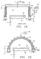
- FIG. 1A illustrates a top portion of a plasma reactor of the type disclosed in European Patent Document No. 0 520 519 A1 and in European Patent Document No. 0 552 491 A1, the disclosures of which are incorporated herein by reference.
- the plasma reactor of FIG. 1A has a generally cylindrical vacuum chamber 10, a gas inlet 11 on top of the chamber 10 for supplying a gas into the chamber interior from which a plasma is to be ignited, a cylindrical RF coil 12 wound around the exterior of the cylindrical chamber 10, a grounded top conducting lid 14 immediately above the coil 12 and a grounded side wall 16 immediately below the coil 12.
- the cylindrical RF coil 12 provides RF energy to generate a high density plasma inside the chamber 10 by inductive coupling while the conductive lid 14 is grounded to assure a grounding path for bias RF power (17) applied to a pedestal 18 supporting a semiconductor wafer 20 at the bottom of the chamber 10.
- One end 12a of the cylindrical coil 12 (e.g., the end nearest the lid) is "hot” because it is connected to the output of an RF source 22, while the opposite end is grounded.
- the coil may be a single section tapped near its center to the RF source.
- FIG. 1B illustrates a recent variation from the apparatus of FIG. 1A in which the ceiling 14 is an insulator and both the ceiling 14 and the RF coil 12 have a dome shape, the RF coil 12 being wound in a conical helix to conform with the ceiling 14, as shown in FIG. 1C.
- the problem with the inductive RF coil having one end grounded and one end RF powered is that the RF peak-to-peak potential within the coil is very high and this causes strong capacitive coupling of RF power into the plasma.
- the high electric potential also causes a significant sputtering of chamber interior surfaces. Such sputtering is undesireable because it produces contamination harmful to the processing of the wafer.
- the RF potential within the coil also affects capacitive coupling of RF power from the coil to the wafer pedestal through the semiconductor wafer being processed.
- a high RF potential may cause a high plasma potential so as to increase the rate of physical sputtering of the wafer being processed. It is desired to control the sputtering rate of the wafer being processed by the RF bias power applied to the wafer pedestal. However, such control is distorted to a certain extent by the high capacitive coupling from the RF coil.
- the term sputtering of the wafer refers to the removal of material from the wafer through the kinetic energy of heavy ions in the plasma colliding with the material being removed. This is different from the removal of material from the wafer by etching.
- Etching involves a chemical reaction between the material being removed and chemical species in the plasma and is not primarily dependent upon kinetic energy of ions or radicals in the plasma.
- Sputtering can have beneficial uses in an etch process. For example, in etching a metal such as aluminum, alloy impurities in the aluminum (such as copper) etch very slowly relative to the aluminum and are best removed at the same rate as the aluminum by sputtering. This requires that the RF potential of the wafer pedestal be set to a level such that the sputtering rate of the copper impurity is about the same as the ethc rate of the aluminum, in this example.
- Capacitive coupling from the RF coil and RF power dissipation are advantageously reduced in the present invention by employing plural coil sections, with each coil section being connected across an RF source and being arranged so that current flow in adjacent coil sections creates magnetic fields having the same direction. Preferably, this is accomplished by winding adjacent coil sections in opposing directions while tapping the adjacent coil sections to a common point which is either the RF source or ground.
- Capacitive coupling and RF power dissipation is further reduced by employing a top lid having an outer insulating annulus and an inner conducting disk portion, the conducting disk portion being displaced or spaced apart from the coil by the width of the annulus. This displacement significantly reduces the RF power dissipation or coupling from the top winding of the coil to the lid.
- FIG. 1A is a simplified drawing of a portion of the plasma reactor of the prior art.
- FIG. 1B is a simplified drawing of a portion of a plasma reactor in accordance with a recent development having a dome ceiling and conically helical RF coil on the ceiling.
- FIG. 1C illustrates the RF coil of FIG. 1B.
- FIG. 2A is a simplified drawing of a portion of a plasma reactor embodying the present invention.
- FIG. 2B illustrates an embodiment corresponding to FIG. 2A but having a dome-shaped lid and RF coil wound thereabout.
- FIG. 2C illustrates the RF coil of FIG. 2B.
- FIG. 2D illustrates a variation of the embodiment of FIG. 2B
- FIG. 3 is a circuit diagram of a mirror coil employed in the plasma reactor of FIG. 2A.
- FIG. 4 is a detailed drawing of a preferred implementation of a conducting lid embodying one aspect of the present invention.
- FIG. 5 is a schematic diagram of a three-section coil in accordance with another embodiment of the invention.
- FIG. 6A is a graph illustrating the time domain waveform of the RF signal on the conventional RF coil of FIG. 1C and the induced capacitive RF current on the wafer pedestal prior to plasma ignition.
- FIG. 6B is a graph illustrating the time domain waveform of the RF signal on the mirror RF coil of FIG. 2C and the induced capacitive RF current on the wafer pedestal prior to plasma ignition.
- FIG. 7A is a graph illustrating the time domain waveform of the RF signal on the conventional RF coil of FIG. 1C and the induced RF current on the wafer pedestal following plasma ignition.
- FIG. 7B is a graph illustrating the time domain waveform of the RF signal on the mirror RF coil of FIG. 2B and the induced RF current on the wafer pedestal following plasma ignition.
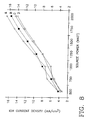
- FIG. 8 is a graph comparing the ion current density obtained with conventional RF coil of FIG. 1C with the ion current density obtained with the mirror RF coil of FIG. 2C as a function of RF power on the coil.
- FIG. 9 is a graph comparing oxide sputtering rates obtained with the conventional RF coil of FIG. 1C with the oxide sputtering rates obtained with the mirror RF coil of FIG. 2C as a function of RF power on the coil in an Ar plasma at 600 watts RF bias power on the wafer pedestal.
- RF power dissipation is advantageously reduced by a top lid 24 having an outer insulating annulus 26 and an inner conducting disk portion 28, the conducting disk portion 28 being displaced or spaced apart from the coil 12 by the width W of the annulus 26.
- This displacement reduces the RF power dissipation or coupling from the top winding of the coil 12 to the lid 24, particularly where the top end 12a of the coil is connected to the RF source 22.
- RF power dissipation is further reduced by grounding the top and bottom ends 12a, 12b of the coil 12 and connecting the RF power source to the middle 12c of the coil in a mirror configuration, as indicated in FIG. 2A and as shown more clearly in the circuit diagram of FIG. 3.
- the "hot" portion of the coil 12 is neither adjacent the grounded conductive portion 28 of the lid 24 nor the grounded lower-most portion of the side wall 16, so that RF power dissipation is reduced accordingly.
- FIG. 2B illustrates how the concept of FIG. 2A is applied to the dome-ceiling plasma reactor of FIG. 1B.
- the ceiling 14 is an insulator.
- the RF power is applied to the middle winding of the coil 12, while the two ends are grounded, as illustrated schematically in FIG. 2C.
- this feature tends to advantageously reduce capacitive coupling to the conductive cylindrical side wall 16.
- grounding the apex of the dome-shaped RF coil 12 of FIG. 2B in the manner illustrated tends to reduce capacitive coupling of the electric field between the coil and the wafer, thereby advantageously increasing inductive coupling.
- FIG. 2D illustrates how the embodiment of FIG. 2B may be modified by replacing the center of the dome 14 with the flat conductive ceiling 28 of FIG. 2A, the coil 12 having an opening therein over the center so that no coil windings overlie the conductive ceiling 28.
- the coil 12 has five windings and the power source 22 applies an RF signal of 2.0 MHz to the middle winding 12c of the coil 12, as disclosed in the above-referenced European Patent Document. Furthermore, all of the operating parameters are as disclosed in detail in the above-referenced European Patent Document and need not be reiterated herein.
- the plasma reactor of FIG. 2A processes 8-inch diameter semiconductor wafers
- the cylindrical reactor chamber 10 has a diameter of about 14 inches
- the conductive disk portion 28 has a diameter of about 8 inches so that the width W of the insulating annulus 26 is about 6 inches.
- the insulating annulus 26 is preferably made of a ceramic such as aluminum oxide or quartz while the conductive disk portion 28 and the conductive side walls 16 are made of anodized aluminum.
- the coil 12 is wound around an insulating cylindrical side wall portion 30 disposed between the lid 24 and the conductive lower portion of the side wall 16.
- the vertical height of the insulating cylindrical side wall portion 30 is about 3.75 inches.
- the insulating side wall portion is preferably made of aluminum oxide or quartz.
- FIG. 4 illustrates a preferred design of the lid 24 of FIG. 2A.
- the gas inlet 11 extends through an axial hole in the center of the conductive disk portion 28 of the lid into a gas distribution manifold of which the conductive disk portion 28 is the ceiling.
- the conductive disk portion 28 is seated on an annular ridge of the insulating annulus 26.
- FIG. 3 illustrates an embodiment in which the coil 12 constitutes two groups of coils connected in parallel to the RF source 22, RF power can be delivered to n groups of inductive coils, where n is an integer greater than 1.
- Each group of coils has a certain number of turns, which number may not be the same from group to group.
- An advantage of having more than one group of coils in the coil 12 is that capacitive coupling to the plasma is significantly reduced for a given applied RF power level as compared to a single inductive coil configuration.
- the single inductive coil configuration (corresponding to FIG.
- the RF inductive coil 12 is preferably separated into n parallel plural coil sections, where n is an integer greater than 1 (e.g., 2, 3, 4, ... etc.) as illustrated in FIGS. 2C, 3 and 5.
- n is an integer greater than 1 (e.g., 2, 3, 4, ... etc.) as illustrated in FIGS. 2C, 3 and 5.
- the RF coil 12 has a cylindrical shape, the n coil sections are mirror images of one another. In all cases it is preferable that the n coil sections are wound such that current in all sections rotates in the same direction so as to produce magnetic fields having the same direction so as to reinforce each other in inductively coupling RF power to the plasma. Preferably, this is accomplished whenever adjacent coils are connected to a common tap point (i.e., the RF source) by winding adjacent coil sections in opposite directions, as in FIGS. 2C, 3 and 5.
- a common tap point i.e., the RF source
- the lower coil section in FIG. 5 labelled “C” adjacent the coil section “B” is wound in the rotational direction of coil section "A” and is connected between the grounded lower end of coil section "B” and the common tap between coil sections "A” and "B” to which the RF source is connected.
- the plural coil sections are grouped by pairs of coil sections, each coil section being within two adjacent pairs of coil sections, each pair of coil sections having a common tap to one end of each coil section in the pair, coil sections within each of pair being wound in opposite directions, the common taps of alternate ones of the pairs being connected to the RF power terminal and the common taps of remaining ones of the pairs being connected to RF ground.
- the coil sections labelled "A” and "B” are one pair having a common tap connected to the RF source
- the coil sections labelled "B” and “C” are a second pair having a common tap connected to RF ground, the coil sections in each pair being wound in opposite rotational directions.
- FIGS. 6A and 6B indicate the induced AC voltage (waveform "A") and current (waveform "B") on the cathode or wafer pedestal in the absence of a plasma by the conventional and mirror coils, respectively, under the following conditions: chamber pressure is pumped down to the desired or baseline operating pressure, there is no gas flow and there is no plasma.
- the AC current induced on the wafer pedestal (an indicia of capacitive coupling) by the mirror coil (FIG. 6B) is lower than the AC current induced by the conventional coil (FIG. 6A).
- the absolute value is too small to measure.
- FIGS. 7A and 7B indicate the AC voltage (waveform "A") and current (waveform "B") induced on the wafer pedestal by a conventional coil and the mirror coil, respectively, with Argon gas present in the vacuum chamber and the plasma ignited.
- the AC current induced on the wafer pedestal by the mirror coil is about 15% less than that induced by the conventional coil, indicating less capacitive coupling with the mirror coil. This is a significant advantage because less capacitive coupling from the mirror coil means that more RF energy is being coupled inductively to generate a plasma with greater density, and the user is better able to control or reduce the ion energy or sputtering rate by varying RF power on the the wafer pedestal.
- the AC current measured during such tests may not necessarily arise from capacitive coupling alone, but may arise from a mixture of both capacitive and inductive coupling.
- FIG. 8 compares the ion current densities with respect to the RF power obtained from a conventional RF coil with that obtained from a mirror coil.
- the curve labelled "A” and having diamond markers represents measurements at the edge of a conventional coil.
- the curve labelled "B” and having black solid square markers represents measurements in the center of the mirror coil.
- the curve labelled "C” and having triangle markers represents measurements at the edge of the conventional coil.
- the curve labelled "D” and having white square markers represents measurements at the edge of the mirror coil. There is no noticeable difference in these measurements between the mirror coil and the conventional coil, due to large random variations. Both the conventional coil and the mirror coil are of cylindrical shapes in this comparison.
- FIG. 9 compares the oxide sputtering rate in an Argon plasma as a function of RF power obtained from a conventional RF coil with that obtained from a mirror coil.
- the curves labelled "A” and “C” with diamond and triangle markers respectively represent mearsurements from two different tests of the mirror coil.
- the curve labelled "B” with the square markers represents measurements on a conventional coil.
- a 600 Watt RF bias signal was applied to the wafer pedestal.
- the sputtering rate predominantly depends upon the RF bias power applied to the wafer pedestal, not the RF power capacitively coupled from the RF coil. Such capacitive coupling should be significantly reduced in the mirror coil, a significant advantage as explained above.
- Another advantage realized in the present invention relates to the sputtering of materials from the chamber interior surfaces. It is very common to operate the source RF power at a very high level (e.g., 2-3 kW with 5kV to 6kV peak-to-peak voltage). At such high voltage levels, the plasma tends to sputter the chamber materials at significant sputtering rates. However, the mirror coil or the plural section coil reduces the peak-to-peak voltage. This reduces the chamber material sputtering rate, thus reducing the rate of contamination of the wafer due to emanation of particles from the sputtering of the chamber wall. This also minimizes device damage on the wafer being processed resulting from such a high RF potential.
Abstract
Description
- The invention is related to plasma reactors for processing semiconductor wafers of the type having a vacuum chamber, an inductive RF coil wound around the upper portion of the chamber and a wafer pedestal which may be capacitively RF powered.
- An inductively coupled RF plasma reactor for processing semiconductor wafers generally includes a vacuum chamber, an inductive RF coil wound around the upper portion of the chamber, a gas supply inlet for furnishing gas to the chamber interior and a wafer pedestal which may be capacitively RF powered. One example is disclosed in U.S. Patent No. 4,948,458 to Ogle. The upper portion of the chamber including the chamber top has a certain area made of insulator material so that RF power from the RF coil can inductively couple into the plasma inside the chamber. The upper portion of the vacuum chamber may be a cylinder while the top may be a flat disk. The cylinder is an insulator with the inductive RF coil wound around it. The flat top of the chamber may be a conductor.
- FIG. 1A illustrates a top portion of a plasma reactor of the type disclosed in European Patent Document No. 0 520 519 A1 and in European Patent Document No. 0 552 491 A1, the disclosures of which are incorporated herein by reference. The plasma reactor of FIG. 1A has a generally
cylindrical vacuum chamber 10, agas inlet 11 on top of thechamber 10 for supplying a gas into the chamber interior from which a plasma is to be ignited, acylindrical RF coil 12 wound around the exterior of thecylindrical chamber 10, a groundedtop conducting lid 14 immediately above thecoil 12 and agrounded side wall 16 immediately below thecoil 12. Thecylindrical RF coil 12 provides RF energy to generate a high density plasma inside thechamber 10 by inductive coupling while theconductive lid 14 is grounded to assure a grounding path for bias RF power (17) applied to apedestal 18 supporting asemiconductor wafer 20 at the bottom of thechamber 10. Oneend 12a of the cylindrical coil 12 (e.g., the end nearest the lid) is "hot" because it is connected to the output of anRF source 22, while the opposite end is grounded. In FIG. 6 and FIG. 8 of European Patent Document No. 0 552 491, the coil may be a single section tapped near its center to the RF source. - FIG. 1B illustrates a recent variation from the apparatus of FIG. 1A in which the
ceiling 14 is an insulator and both theceiling 14 and theRF coil 12 have a dome shape, theRF coil 12 being wound in a conical helix to conform with theceiling 14, as shown in FIG. 1C. - One problem with such a plasma reactor is that the close proximity of the
grounded lid 14 to the "hot" end of thecylindrical coil 12 of FIG. 1A orconical helix coil 12 of FIG. 1B permits significant dissipation of the RF power from thecoil 12 to thegrounded lid 14. Alternatively, if the bottom end of thecoil 12 is "hot" and the top end is grounded, then RF power is dissipated from thecoil 12 to thegrounded side wall 16. As a result, the required RF power level for thecylindrical coil 12 is on the order of 2 to 3 watts, which is comparatively high. Because of the need to ground thelid 14 above thecoil 12 and theside wall 16 below thecoil 12, such RF power dissipation from thecoil 12 has seemed to be unavoidable. - The problem with the inductive RF coil having one end grounded and one end RF powered is that the RF peak-to-peak potential within the coil is very high and this causes strong capacitive coupling of RF power into the plasma. The high electric potential also causes a significant sputtering of chamber interior surfaces. Such sputtering is undesireable because it produces contamination harmful to the processing of the wafer.
- The RF potential within the coil also affects capacitive coupling of RF power from the coil to the wafer pedestal through the semiconductor wafer being processed. A high RF potential may cause a high plasma potential so as to increase the rate of physical sputtering of the wafer being processed. It is desired to control the sputtering rate of the wafer being processed by the RF bias power applied to the wafer pedestal. However, such control is distorted to a certain extent by the high capacitive coupling from the RF coil. As employed herein, the term sputtering of the wafer refers to the removal of material from the wafer through the kinetic energy of heavy ions in the plasma colliding with the material being removed. This is different from the removal of material from the wafer by etching. Etching involves a chemical reaction between the material being removed and chemical species in the plasma and is not primarily dependent upon kinetic energy of ions or radicals in the plasma. Sputtering can have beneficial uses in an etch process. For example, in etching a metal such as aluminum, alloy impurities in the aluminum (such as copper) etch very slowly relative to the aluminum and are best removed at the same rate as the aluminum by sputtering. This requires that the RF potential of the wafer pedestal be set to a level such that the sputtering rate of the copper impurity is about the same as the ethc rate of the aluminum, in this example.
- Capacitive coupling from the RF coil and RF power dissipation are advantageously reduced in the present invention by employing plural coil sections, with each coil section being connected across an RF source and being arranged so that current flow in adjacent coil sections creates magnetic fields having the same direction. Preferably, this is accomplished by winding adjacent coil sections in opposing directions while tapping the adjacent coil sections to a common point which is either the RF source or ground. Capacitive coupling and RF power dissipation is further reduced by employing a top lid having an outer insulating annulus and an inner conducting disk portion, the conducting disk portion being displaced or spaced apart from the coil by the width of the annulus. This displacement significantly reduces the RF power dissipation or coupling from the top winding of the coil to the lid.
- The following is a description of some specific embodiments of the invention, reference being made to the accompanying drawings, in which:
- FIG. 1A is a simplified drawing of a portion of the plasma reactor of the prior art.
- FIG. 1B is a simplified drawing of a portion of a plasma reactor in accordance with a recent development having a dome ceiling and conically helical RF coil on the ceiling.
- FIG. 1C illustrates the RF coil of FIG. 1B.
- FIG. 2A is a simplified drawing of a portion of a plasma reactor embodying the present invention.
- FIG. 2B illustrates an embodiment corresponding to FIG. 2A but having a dome-shaped lid and RF coil wound thereabout.
- FIG. 2C illustrates the RF coil of FIG. 2B.
- FIG. 2D illustrates a variation of the embodiment of FIG. 2B
- FIG. 3 is a circuit diagram of a mirror coil employed in the plasma reactor of FIG. 2A.
- FIG. 4 is a detailed drawing of a preferred implementation of a conducting lid embodying one aspect of the present invention.
- FIG. 5 is a schematic diagram of a three-section coil in accordance with another embodiment of the invention.
- FIG. 6A is a graph illustrating the time domain waveform of the RF signal on the conventional RF coil of FIG. 1C and the induced capacitive RF current on the wafer pedestal prior to plasma ignition.
- FIG. 6B is a graph illustrating the time domain waveform of the RF signal on the mirror RF coil of FIG. 2C and the induced capacitive RF current on the wafer pedestal prior to plasma ignition.
- FIG. 7A is a graph illustrating the time domain waveform of the RF signal on the conventional RF coil of FIG. 1C and the induced RF current on the wafer pedestal following plasma ignition.
- FIG. 7B is a graph illustrating the time domain waveform of the RF signal on the mirror RF coil of FIG. 2B and the induced RF current on the wafer pedestal following plasma ignition.
- FIG. 8 is a graph comparing the ion current density obtained with conventional RF coil of FIG. 1C with the ion current density obtained with the mirror RF coil of FIG. 2C as a function of RF power on the coil.
- FIG. 9 is a graph comparing oxide sputtering rates obtained with the conventional RF coil of FIG. 1C with the oxide sputtering rates obtained with the mirror RF coil of FIG. 2C as a function of RF power on the coil in an Ar plasma at 600 watts RF bias power on the wafer pedestal.
- Referring to FIG. 2A, RF power dissipation is advantageously reduced by a
top lid 24 having an outer insulatingannulus 26 and an innerconducting disk portion 28, theconducting disk portion 28 being displaced or spaced apart from thecoil 12 by the width W of theannulus 26. This displacement reduces the RF power dissipation or coupling from the top winding of thecoil 12 to thelid 24, particularly where thetop end 12a of the coil is connected to theRF source 22. - RF power dissipation is further reduced by grounding the top and bottom ends 12a, 12b of the
coil 12 and connecting the RF power source to the middle 12c of the coil in a mirror configuration, as indicated in FIG. 2A and as shown more clearly in the circuit diagram of FIG. 3. In this way, the "hot" portion of thecoil 12 is neither adjacent the groundedconductive portion 28 of thelid 24 nor the grounded lower-most portion of theside wall 16, so that RF power dissipation is reduced accordingly. - FIG. 2B illustrates how the concept of FIG. 2A is applied to the dome-ceiling plasma reactor of FIG. 1B. As in FIG. 1B, the
ceiling 14 is an insulator. As in the embodiment of FIG. 2A, in FIG. 2B the RF power is applied to the middle winding of thecoil 12, while the two ends are grounded, as illustrated schematically in FIG. 2C. In many cases, this feature tends to advantageously reduce capacitive coupling to the conductivecylindrical side wall 16. Moreover, in many cases grounding the apex of the dome-shapedRF coil 12 of FIG. 2B in the manner illustrated tends to reduce capacitive coupling of the electric field between the coil and the wafer, thereby advantageously increasing inductive coupling. FIG. 2D illustrates how the embodiment of FIG. 2B may be modified by replacing the center of thedome 14 with the flatconductive ceiling 28 of FIG. 2A, thecoil 12 having an opening therein over the center so that no coil windings overlie theconductive ceiling 28. - In a preferred implementation of the embodiment of FIG. 2A, the
coil 12 has five windings and thepower source 22 applies an RF signal of 2.0 MHz to the middle winding 12c of thecoil 12, as disclosed in the above-referenced European Patent Document. Furthermore, all of the operating parameters are as disclosed in detail in the above-referenced European Patent Document and need not be reiterated herein. - In a preferred implementation, the plasma reactor of FIG. 2A processes 8-inch diameter semiconductor wafers, the
cylindrical reactor chamber 10 has a diameter of about 14 inches, theconductive disk portion 28 has a diameter of about 8 inches so that the width W of the insulatingannulus 26 is about 6 inches. The insulatingannulus 26 is preferably made of a ceramic such as aluminum oxide or quartz while theconductive disk portion 28 and theconductive side walls 16 are made of anodized aluminum. Thecoil 12 is wound around an insulating cylindricalside wall portion 30 disposed between thelid 24 and the conductive lower portion of theside wall 16. The vertical height of the insulating cylindricalside wall portion 30 is about 3.75 inches. The insulating side wall portion is preferably made of aluminum oxide or quartz. - FIG. 4 illustrates a preferred design of the
lid 24 of FIG. 2A. Thegas inlet 11 extends through an axial hole in the center of theconductive disk portion 28 of the lid into a gas distribution manifold of which theconductive disk portion 28 is the ceiling. Theconductive disk portion 28 is seated on an annular ridge of the insulatingannulus 26. - While FIG. 3 illustrates an embodiment in which the
coil 12 constitutes two groups of coils connected in parallel to theRF source 22, RF power can be delivered to n groups of inductive coils, where n is an integer greater than 1. Each group of coils has a certain number of turns, which number may not be the same from group to group. For example, FIG. 5 illustrates a coil for n=3 to be used in place of thecoil 12 of FIG. 1A. An advantage of having more than one group of coils in thecoil 12 is that capacitive coupling to the plasma is significantly reduced for a given applied RF power level as compared to a single inductive coil configuration. For example, the single inductive coil configuration (corresponding to FIG. 1A) with seven coil turns was observed to have a voltage drop across the coil of 6 kV RMS for an applied power level of 2 kW, with the capacitor C₁ having 2000 picoFarads capacitance and the capacitor C₂ having 275 picoFarads capacitance. In contrast, at the same applied RF power level (2 kW), the mirror coil of FIGS. 2 and 3 (n=2) with three coil turns in each of the two groups exhibited a voltage drop of only 3 kV RMS and 2 kV RMS, respectively. - As stated above with reference to FIG. 3, the RF
inductive coil 12 is preferably separated into n parallel plural coil sections, where n is an integer greater than 1 (e.g., 2, 3, 4, ... etc.) as illustrated in FIGS. 2C, 3 and 5. If theRF coil 12 has a cylindrical shape, the n coil sections are mirror images of one another. In all cases it is preferable that the n coil sections are wound such that current in all sections rotates in the same direction so as to produce magnetic fields having the same direction so as to reinforce each other in inductively coupling RF power to the plasma. Preferably, this is accomplished whenever adjacent coils are connected to a common tap point (i.e., the RF source) by winding adjacent coil sections in opposite directions, as in FIGS. 2C, 3 and 5. - Referring to FIG. 3 for example, current flow through the upper coil section from the
common tap point 12c to thecoil end 12a is upward while current flow is downward through the lower coil section from thecommon tap point 12c tocoil end 12b. However, rotation of the current through the coil loops is in the same rotational direction in both sections because the two coil sections are wound in opposite directions. Thus, the magnetic fields produced by both coil sections have the same polarity and reinforce each other. - Referring to FIG. 5 in which there are three coil sections labelled "A", "B" and "C" for the case n=3, the upper two coil sections "A" and "B" correspond to the two coil sections of FIG. 3, consisting of coiled conductors wound in opposite rotational directions. The lower coil section in FIG. 5 labelled "C" adjacent the coil section "B" is wound in the rotational direction of coil section "A" and is connected between the grounded lower end of coil section "B" and the common tap between coil sections "A" and "B" to which the RF source is connected.
- In general, for n>2, the plural coil sections are grouped by pairs of coil sections, each coil section being within two adjacent pairs of coil sections, each pair of coil sections having a common tap to one end of each coil section in the pair, coil sections within each of pair being wound in opposite directions, the common taps of alternate ones of the pairs being connected to the RF power terminal and the common taps of remaining ones of the pairs being connected to RF ground. Thus, for example, in FIG. 5, the coil sections labelled "A" and "B" are one pair having a common tap connected to the RF source, the coil sections labelled "B" and "C" are a second pair having a common tap connected to RF ground, the coil sections in each pair being wound in opposite rotational directions.
- FIGS. 6A and 6B indicate the induced AC voltage (waveform "A") and current (waveform "B") on the cathode or wafer pedestal in the absence of a plasma by the conventional and mirror coils, respectively, under the following conditions: chamber pressure is pumped down to the desired or baseline operating pressure, there is no gas flow and there is no plasma. The AC current induced on the wafer pedestal (an indicia of capacitive coupling) by the mirror coil (FIG. 6B) is lower than the AC current induced by the conventional coil (FIG. 6A). However, the absolute value is too small to measure.
- FIGS. 7A and 7B indicate the AC voltage (waveform "A") and current (waveform "B") induced on the wafer pedestal by a conventional coil and the mirror coil, respectively, with Argon gas present in the vacuum chamber and the plasma ignited. The AC current induced on the wafer pedestal by the mirror coil is about 15% less than that induced by the conventional coil, indicating less capacitive coupling with the mirror coil. This is a significant advantage because less capacitive coupling from the mirror coil means that more RF energy is being coupled inductively to generate a plasma with greater density, and the user is better able to control or reduce the ion energy or sputtering rate by varying RF power on the the wafer pedestal. The AC current measured during such tests may not necessarily arise from capacitive coupling alone, but may arise from a mixture of both capacitive and inductive coupling.
- FIG. 8 compares the ion current densities with respect to the RF power obtained from a conventional RF coil with that obtained from a mirror coil. The curve labelled "A" and having diamond markers represents measurements at the edge of a conventional coil. The curve labelled "B" and having black solid square markers represents measurements in the center of the mirror coil. The curve labelled "C" and having triangle markers represents measurements at the edge of the conventional coil. The curve labelled "D" and having white square markers represents measurements at the edge of the mirror coil. There is no noticeable difference in these measurements between the mirror coil and the conventional coil, due to large random variations. Both the conventional coil and the mirror coil are of cylindrical shapes in this comparison.
- FIG. 9 compares the oxide sputtering rate in an Argon plasma as a function of RF power obtained from a conventional RF coil with that obtained from a mirror coil. The curves labelled "A" and "C" with diamond and triangle markers respectively represent mearsurements from two different tests of the mirror coil. The curve labelled "B" with the square markers represents measurements on a conventional coil. As in the comparison of FIG. 8, there is no noticeable difference due to large random variations. In the test of FIG. 9, a 600 Watt RF bias signal was applied to the wafer pedestal. The sputtering rate predominantly depends upon the RF bias power applied to the wafer pedestal, not the RF power capacitively coupled from the RF coil. Such capacitive coupling should be significantly reduced in the mirror coil, a significant advantage as explained above.
- The foregoing comparisons involved only the mirror coil embodiment of the invention, in which n=2. However, it should be noted that for all other embodiments of the invention, in which n>2, these advantages generally are more pronounced because there is an even greater division of the potential in the coil.
- Another advantage realized in the present invention relates to the sputtering of materials from the chamber interior surfaces. It is very common to operate the source RF power at a very high level (e.g., 2-3 kW with 5kV to 6kV peak-to-peak voltage). At such high voltage levels, the plasma tends to sputter the chamber materials at significant sputtering rates. However, the mirror coil or the plural section coil reduces the peak-to-peak voltage. This reduces the chamber material sputtering rate, thus reducing the rate of contamination of the wafer due to emanation of particles from the sputtering of the chamber wall. This also minimizes device damage on the wafer being processed resulting from such a high RF potential.
- While the invention has been described in detail by specific reference to preferred embodiments, it is understood that variations and modifications thereof may be made without departing from the true spirit and scope of the invention.
Claims (32)
- A plasma reactor comprising:
a vacuum chamber having an at least partially insulating upper portion;
an RF power source having an RF power terminal and a return terminal connected to an RF ground;
an RF inductor coil wound around said insulating upper portion, said RF inductor coil comprising plural coil sections each connected across said RF power terminal and said RF ground, each one of said coil sections being wrapped around said insulating upper portion, at least a pair of said coil sections being connected at respective ends thereof through a common tap point to said RF power terminal and each coil section of said pair being wound in opposite rotational directions;
means for supplying a gas into said chamber;
a wafer pedestal in said chamber for supporting a wafer to be processing inside said chamber. - The reactor of Claim 1 wherein said insulating upper portion comprises a top cylindrical side wall portion, said chamber further comprising a lower conductive cylindrical side wall portion.
- The reactor of Claim 2 further comprising a ceiling overlying said top cylindrical side wall portion, said ceiling having a conductive center portion and an insulating annular portion adjacent said cylindrical side wall and surrounding said conductive center portion.
- The reactor of Claim 3 wherein said second ends of said coil sections are adjacent respective ones of said conductive lower side wall portion, and wherein said conductive center portion of said ceiling and said lower conductive portion of said side wall are connected to said RF ground.
- The reactor of Claim 1 wherein said insulating upper portion comprises at least a first portion of a dome top of said chamber.
- The reactor of Claim 5 wherein said dome top comprises a second portion which is a conductive center section at an apex of said dome top and an insulating annulus surrounding said conductive center section, said RF inductor being wound only around said first portion of said dome top.
- The reactor of Claim 6 wherein said second ends of said coil sections are adjacent respective ones of said conductive lower side wall portion and said second portion of said dome top, and wherein said conductive center section of said dome top and said lower conductive portion of said side wall are connected to said RF ground.
- The reactor of Claim 5 wherein said upper portion comprises the entire dome top and said RF inductor coil is wound around the entirety of said dome top.
- The reactor of Claim 1 wherein said RF inductor coil comprises a helically wound conductor having a pair of ends and a middle, said coil being divided into said two sections at said middle, and wherein said middle comprises said first terminals and said pair of ends comprises said second terminals.
- The reactor of Claim 9 wherein said helically wound conductor is wound in a cylinder shape and wherein said two sections are mirror coils.
- The reactor of Claim 1 wherein said insulating annulus comprises a ceramic material.
- The reactor of Claim 11 wherein said ceramic material comprises aluminum oxide.
- The reactor of Claim 1 further comprising a third coil section connected at one end thereof to said RF ground at a second common tap point with an end of one of said pair of coil sections, said third coil section and said one of said pair of coil sections being wound in opposite directions.
- The reactor of Claim 1 wherein said plural coil sections comprise pairs of coil sections, a respective coil section being within two of said pairs of coil sections, each pair of coil sections having a common tap to one end of each coil section in the pair of coil sections, coil sections within each of pair being wound in opposite directions, the common taps of alternate ones of said pairs being connected to said RF power terminal and the common taps of remaining ones of said pairs being connected to said RF ground.
- A plasma reactor comprising:
a vacuum chamber having a containment wall;
means for introducing a gas into said vacuum chamber;
an RF source;
an RF coil wound around a first portion of said containment wall and comprising plural coil sections, at least two of said plural coil sections being wound in opposite directions and having facing ends connected at a first common tap to said RF source and their other ends connected to ground. - The reactor of Claim 15 further comprising a third coil section connected at one end thereof to ground at a second common tap point with an end of one of said pair of coil sections, said third coil section and said one of said pair of coil sections being wound in opposite directions.
- The reactor of Claim 15 wherein said plural coil sections comprise pairs of coil sections, a respective coil section being within two of said pairs of coil sections, each pair of coil sections having a common tap to one end of each coil section in the pair of coil sections, coil sections within each of pair being wound in opposite directions, the common taps of alternate ones of said pairs being connected to said RF source terminal and the common taps of remaining ones of said pairs being connected to ground.
- The plasma reactor of Claim 15 wherein there are two coil sections and said coil is connected to said RF source in a mirror configuration.
- The plasma reactor of Claim 15 wherein said first portion of said containment wall comprises a cylindrical side wall having a conductive section thereof below said coil and a lid above said coil, said lid having a conductive portion thereof spaced apart from said cylindrical side wall, a remaining portion of said lid between said conductive portion and said side wall being insulative.
- The plasma reactor of Claim 19 wherein said conductive portion of said lid and said conductive section of said side wall are both connected to an RF return node of said RF source.
- The plasma reactor of Claim 20 wherein said RF return node is a ground node.
- The plasma reactor of Claim 15 wherein said first portion of said containment wall comprises a dome-shaped lid, and another portion of said containment wall comprises a conductive side wall.
- The plasma reactor of Claim 22 wherein said coil is wound as a conical helix conforming with said dome-shaped lid, and wherein one there are two of said coil sections, said coil being connected in a mirror configuration to said RF source.
- The plasma reactor of Claim 23 wherein an upper one of said sections has an end at the apex of said dome-shaped lid, said end being connected to an RF return node of said RF source.
- The plasma reactor of Claim 22 wherein said dome-shaped lid is comprised of insulative material.
- The reactor of Claim 24 wherein each section has a pair of ends, one end being connected to said RF source and the other end connected to an RF return node of said RF source.
- The reactor of Claim 26 wherein there are two of said sections, and said RF coil comprises a helically wound conductor having a pair of ends and a middle, said coil being divided into said two sections at said middle, and wherein said middle is connected by a conductor to said RF source and wherein said pair of ends are both connected to an RF return node of said RF source.
- A plasma reactor, comprising:
a vacuum chamber shell comprising two conductive shell sections and an insulating shell section between said two conductive shell sections, said two conductive shell sections being connected to a return conductive path;
means for introducing a processing gas into said vacuum chamber;
an RF coil antenna wound around said insulating shell section and having at least two coil ends adjacent respective ones of said two conductive shell sections, said two coil ends being connected to said return conductive path so as to be at the same electrical potential as said two conductive shell sections; and
an RF power source having a power terminal connected to said RF coil antenna at a point intermediate said two coil ends and an RF return terminal connected to said return conductive path. - The reactor of Claim 28 wherein said return path is RF ground.
- A plasma reactor, comprising:
a vacuum chamber shell comprising a conductive shell section and an insulating shell section adjacent said conductive shell section, said conductive shell section being connected to a return conductive path;
means for introducing a processing gas into said chamber;
an RF coil antenna wound around said insulating shell section and having two coil ends, one of said two coil ends being adjacent said conductive shell section, said two coil ends being connected to said return conductive path so that said one coil end is at the same electrical potential as said conductive shell section; and
an RF power source having a power terminal connected to said RF coil antenna at a point intermediate said two coil ends and an RF return terminal connected to said return conductive path. - The reactor of Claim 30 wherein said return path is RF ground.
- The reactor of Claim 30 wherein said RF coil antenna is wound in a first direction from one of said two coil ends to said point intermediate said two coil ends and is wound in an opposite direction from the other of said two coil ends to said point intermediate said two coil ends.
Applications Claiming Priority (2)
| Application Number | Priority Date | Filing Date | Title |
|---|---|---|---|
| US277531 | 1994-07-18 | ||
| US08/277,531 US5540824A (en) | 1994-07-18 | 1994-07-18 | Plasma reactor with multi-section RF coil and isolated conducting lid |
Publications (3)
| Publication Number | Publication Date |
|---|---|
| EP0694949A2 true EP0694949A2 (en) | 1996-01-31 |
| EP0694949A3 EP0694949A3 (en) | 1998-12-16 |
| EP0694949B1 EP0694949B1 (en) | 2001-12-19 |
Family
ID=23061269
Family Applications (1)
| Application Number | Title | Priority Date | Filing Date |
|---|---|---|---|
| EP95304041A Expired - Lifetime EP0694949B1 (en) | 1994-07-18 | 1995-06-12 | Inductively coupled plasma reactors |
Country Status (6)
| Country | Link |
|---|---|
| US (1) | US5540824A (en) |
| EP (1) | EP0694949B1 (en) |
| JP (1) | JP3929514B2 (en) |
| KR (1) | KR960005832A (en) |
| AT (1) | ATE211304T1 (en) |
| DE (1) | DE69524683T2 (en) |
Cited By (17)
| Publication number | Priority date | Publication date | Assignee | Title |
|---|---|---|---|---|
| WO1997002588A1 (en) * | 1995-06-30 | 1997-01-23 | Lam Research Corporation | Low inductance large area coil for an inductively coupled plasma source |
| EP0786804A2 (en) | 1996-01-26 | 1997-07-30 | Applied Materials, Inc. | Apparatus and method for processing substrates |
| EP0788138A2 (en) * | 1996-02-02 | 1997-08-06 | Applied Materials, Inc. | Plasma reactors for processing substrates |
| WO1997033300A1 (en) * | 1996-03-06 | 1997-09-12 | Mattson Technology, Inc. | Icp reactor having a conically-shaped plasma-generating section |
| EP0810816A1 (en) * | 1996-05-30 | 1997-12-03 | Applied Materials, Inc. | Balanced source for plasma system |
| US5759280A (en) * | 1996-06-10 | 1998-06-02 | Lam Research Corporation | Inductively coupled source for deriving substantially uniform plasma flux |
| US5800619A (en) * | 1996-06-10 | 1998-09-01 | Lam Research Corporation | Vacuum plasma processor having coil with minimum magnetic field in its center |
| WO1999014784A2 (en) * | 1997-09-16 | 1999-03-25 | Lam Research Corporation | Vacuum plasma processor having coil with added conducting segments to its peripheral part |
| US6028285A (en) * | 1997-11-19 | 2000-02-22 | Board Of Regents, The University Of Texas System | High density plasma source for semiconductor processing |
| EP1079671A2 (en) * | 1999-08-26 | 2001-02-28 | Jusung Engineering Co. Ltd. | Antenna device for generating inductively coupled plasma |
| EP1047289A3 (en) * | 1999-04-22 | 2004-01-02 | Applied Materials, Inc. | RF plasma source for material processing |
| US6736931B2 (en) | 1991-06-27 | 2004-05-18 | Kenneth S. Collins | Inductively coupled RF plasma reactor and plasma chamber enclosure structure therefor |
| US6790375B1 (en) | 1998-09-30 | 2004-09-14 | Lam Research Corporation | Dechucking method and apparatus for workpieces in vacuum processors |
| US6965506B2 (en) | 1998-09-30 | 2005-11-15 | Lam Research Corporation | System and method for dechucking a workpiece from an electrostatic chuck |
| EP1608000A2 (en) * | 1996-06-10 | 2005-12-21 | Lam Research Corporation | RF plasma processor |
| DE19781667B4 (en) * | 1996-03-27 | 2007-07-05 | Tokyo Electron Ltd. | Plasma generation method and apparatus having an inductively coupled plasma source |
| CN102056393A (en) * | 2009-10-26 | 2011-05-11 | 应用材料股份有限公司 | Inductively coupled plasma apparatus |
Families Citing this family (59)
| Publication number | Priority date | Publication date | Assignee | Title |
|---|---|---|---|---|
| JP3105403B2 (en) * | 1994-09-14 | 2000-10-30 | 松下電器産業株式会社 | Plasma processing equipment |
| EP0710055B1 (en) | 1994-10-31 | 1999-06-23 | Applied Materials, Inc. | Plasma reactors for processing semi-conductor wafers |
| US5643639A (en) * | 1994-12-22 | 1997-07-01 | Research Triangle Institute | Plasma treatment method for treatment of a large-area work surface apparatus and methods |
| US5688357A (en) * | 1995-02-15 | 1997-11-18 | Applied Materials, Inc. | Automatic frequency tuning of an RF power source of an inductively coupled plasma reactor |
| US6224724B1 (en) | 1995-02-23 | 2001-05-01 | Tokyo Electron Limited | Physical vapor processing of a surface with non-uniformity compensation |
| US6132564A (en) * | 1997-11-17 | 2000-10-17 | Tokyo Electron Limited | In-situ pre-metallization clean and metallization of semiconductor wafers |
| US5907221A (en) * | 1995-08-16 | 1999-05-25 | Applied Materials, Inc. | Inductively coupled plasma reactor with an inductive coil antenna having independent loops |
| US6264812B1 (en) | 1995-11-15 | 2001-07-24 | Applied Materials, Inc. | Method and apparatus for generating a plasma |
| US5900105A (en) * | 1996-07-09 | 1999-05-04 | Gamma Precision Technology, Inc. | Wafer transfer system and method of using the same |
| US5846883A (en) * | 1996-07-10 | 1998-12-08 | Cvc, Inc. | Method for multi-zone high-density inductively-coupled plasma generation |
| US6254737B1 (en) | 1996-10-08 | 2001-07-03 | Applied Materials, Inc. | Active shield for generating a plasma for sputtering |
| US6190513B1 (en) | 1997-05-14 | 2001-02-20 | Applied Materials, Inc. | Darkspace shield for improved RF transmission in inductively coupled plasma sources for sputter deposition |
| TW403959B (en) * | 1996-11-27 | 2000-09-01 | Hitachi Ltd | Plasma treatment device |
| US5948215A (en) * | 1997-04-21 | 1999-09-07 | Tokyo Electron Limited | Method and apparatus for ionized sputtering |
| US5800688A (en) * | 1997-04-21 | 1998-09-01 | Tokyo Electron Limited | Apparatus for ionized sputtering |
| US6158384A (en) * | 1997-06-05 | 2000-12-12 | Applied Materials, Inc. | Plasma reactor with multiple small internal inductive antennas |
| US6178920B1 (en) | 1997-06-05 | 2001-01-30 | Applied Materials, Inc. | Plasma reactor with internal inductive antenna capable of generating helicon wave |
| US6565717B1 (en) | 1997-09-15 | 2003-05-20 | Applied Materials, Inc. | Apparatus for sputtering ionized material in a medium to high density plasma |
| US6132566A (en) * | 1998-07-30 | 2000-10-17 | Applied Materials, Inc. | Apparatus and method for sputtering ionized material in a plasma |
| US6523493B1 (en) * | 2000-08-01 | 2003-02-25 | Tokyo Electron Limited | Ring-shaped high-density plasma source and method |
| US6192829B1 (en) * | 1999-05-05 | 2001-02-27 | Applied Materials, Inc. | Antenna coil assemblies for substrate processing chambers |
| JP2001052894A (en) * | 1999-08-04 | 2001-02-23 | Ulvac Japan Ltd | Inductively coupled high frequency plasma source |
| SE9903675D0 (en) * | 1999-10-13 | 1999-10-13 | Abb Research Ltd | A device and a method for heat treatment of an object in a susceptor |
| US6447636B1 (en) * | 2000-02-16 | 2002-09-10 | Applied Materials, Inc. | Plasma reactor with dynamic RF inductive and capacitive coupling control |
| US6694915B1 (en) * | 2000-07-06 | 2004-02-24 | Applied Materials, Inc | Plasma reactor having a symmetrical parallel conductor coil antenna |
| US6409933B1 (en) | 2000-07-06 | 2002-06-25 | Applied Materials, Inc. | Plasma reactor having a symmetric parallel conductor coil antenna |
| US6414648B1 (en) | 2000-07-06 | 2002-07-02 | Applied Materials, Inc. | Plasma reactor having a symmetric parallel conductor coil antenna |
| US6685798B1 (en) * | 2000-07-06 | 2004-02-03 | Applied Materials, Inc | Plasma reactor having a symmetrical parallel conductor coil antenna |
| US6459066B1 (en) | 2000-08-25 | 2002-10-01 | Board Of Regents, The University Of Texas System | Transmission line based inductively coupled plasma source with stable impedance |
| US6875700B2 (en) * | 2000-08-29 | 2005-04-05 | Board Of Regents, The University Of Texas System | Ion-Ion plasma processing with bias modulation synchronized to time-modulated discharges |
| KR100469889B1 (en) * | 2002-11-14 | 2005-02-02 | 어댑티브프라즈마테크놀로지 주식회사 | Plasma etching apparatus having plurality of coils |
| JP2003282547A (en) * | 2002-03-26 | 2003-10-03 | Ulvac Japan Ltd | Method and apparatus for performing plasma treatment with high selectivity and high uniformity over large area |
| DE10231738B4 (en) * | 2002-07-13 | 2005-03-17 | Deutsches Zentrum für Luft- und Raumfahrt e.V. | An induction plasma torch apparatus and method for electrically controlling an induction plasma torch apparatus |
| DE10231739B4 (en) * | 2002-07-13 | 2004-10-28 | Deutsches Zentrum für Luft- und Raumfahrt e.V. | Induction plasma torch device |
| KR100964398B1 (en) * | 2003-01-03 | 2010-06-17 | 삼성전자주식회사 | Inductively coupled antenna and plasma processing apparatus using the same |
| KR100561848B1 (en) * | 2003-11-04 | 2006-03-16 | 삼성전자주식회사 | Helical resonator type plasma processing apparatus |
| US20050145341A1 (en) * | 2003-11-19 | 2005-07-07 | Masaki Suzuki | Plasma processing apparatus |
| KR101038204B1 (en) * | 2004-02-25 | 2011-05-31 | 주성엔지니어링(주) | Antenna for plasma |
| US20050205211A1 (en) * | 2004-03-22 | 2005-09-22 | Vikram Singh | Plasma immersion ion implantion apparatus and method |
| KR100876050B1 (en) * | 2004-12-28 | 2008-12-26 | 가부시키가이샤 히다치 고쿠사이 덴키 | Substrate processing equipment |
| US8187416B2 (en) * | 2005-05-20 | 2012-05-29 | Applied Materials, Inc. | Interior antenna for substrate processing chamber |
| KR100785401B1 (en) * | 2005-11-04 | 2007-12-13 | 세메스 주식회사 | Inductively coupled plasma treatment apparatus |
| US20070170867A1 (en) * | 2006-01-24 | 2007-07-26 | Varian Semiconductor Equipment Associates, Inc. | Plasma Immersion Ion Source With Low Effective Antenna Voltage |
| US20080132046A1 (en) * | 2006-12-04 | 2008-06-05 | Varian Semiconductor Equipment Associates, Inc. | Plasma Doping With Electronically Controllable Implant Angle |
| US20080169183A1 (en) * | 2007-01-16 | 2008-07-17 | Varian Semiconductor Equipment Associates, Inc. | Plasma Source with Liner for Reducing Metal Contamination |
| US7820533B2 (en) * | 2007-02-16 | 2010-10-26 | Varian Semiconductor Equipment Associates, Inc. | Multi-step plasma doping with improved dose control |
| JP5572329B2 (en) * | 2009-01-15 | 2014-08-13 | 株式会社日立ハイテクノロジーズ | Plasma processing apparatus and plasma generation apparatus |
| JP5410950B2 (en) * | 2009-01-15 | 2014-02-05 | 株式会社日立ハイテクノロジーズ | Plasma processing equipment |
| JP6101031B2 (en) * | 2012-09-28 | 2017-03-22 | 東京応化工業株式会社 | Plasma processing apparatus and laminate manufacturing method |
| US8970114B2 (en) | 2013-02-01 | 2015-03-03 | Lam Research Corporation | Temperature controlled window of a plasma processing chamber component |
| KR102001117B1 (en) * | 2013-11-05 | 2019-07-17 | 어플라이드 머티어리얼스, 인코포레이티드 | Sputter deposition source, apparatus for sputter deposition and method of assembling thereof |
| US10187966B2 (en) * | 2015-07-24 | 2019-01-22 | Applied Materials, Inc. | Method and apparatus for gas abatement |
| KR102026880B1 (en) * | 2016-10-13 | 2019-09-30 | 에이피시스템 주식회사 | Substrate processing apparatus |
| CN107256822B (en) * | 2017-07-27 | 2019-08-23 | 北京北方华创微电子装备有限公司 | Top electrode assembly and reaction chamber |
| CN108770173B (en) * | 2018-07-27 | 2020-11-20 | 上海工程技术大学 | Plasma jet generating device |
| KR20210039451A (en) * | 2018-09-20 | 2021-04-09 | 가부시키가이샤 코쿠사이 엘렉트릭 | Substrate processing apparatus, manufacturing method and program of semiconductor device |
| DE102019213591A1 (en) * | 2019-09-06 | 2021-03-11 | Singulus Technologies Ag | TREATMENT PLANT AND PLASMA TREATMENT PROCESS |
| FR3135731A1 (en) * | 2022-05-17 | 2023-11-24 | Universite Grenoble Alpes | Capacitively coupled plasma-assisted atomic layer deposition process |
| FR3135732A1 (en) * | 2022-05-17 | 2023-11-24 | Universite Grenoble Alpes | Plasma-assisted deposition reactor |
Citations (3)
| Publication number | Priority date | Publication date | Assignee | Title |
|---|---|---|---|---|
| US4948458A (en) | 1989-08-14 | 1990-08-14 | Lam Research Corporation | Method and apparatus for producing magnetically-coupled planar plasma |
| EP0520519A1 (en) | 1991-06-27 | 1992-12-30 | Applied Materials, Inc. | Plasma processing reactor and process for plasma etching |
| EP0552491A1 (en) | 1992-01-24 | 1993-07-28 | Applied Materials, Inc. | Plasma etch process |
Family Cites Families (19)
| Publication number | Priority date | Publication date | Assignee | Title |
|---|---|---|---|---|
| US4464223A (en) * | 1983-10-03 | 1984-08-07 | Tegal Corp. | Plasma reactor apparatus and method |
| KR900007687B1 (en) * | 1986-10-17 | 1990-10-18 | 가부시기가이샤 히다찌세이사꾸쇼 | Method and device for plasma processing |
| GB8629634D0 (en) * | 1986-12-11 | 1987-01-21 | Dobson C D | Reactive ion & sputter etching |
| US4842683A (en) * | 1986-12-19 | 1989-06-27 | Applied Materials, Inc. | Magnetic field-enhanced plasma etch reactor |
| US4872947A (en) * | 1986-12-19 | 1989-10-10 | Applied Materials, Inc. | CVD of silicon oxide using TEOS decomposition and in-situ planarization process |
| DE3738352A1 (en) * | 1987-11-11 | 1989-05-24 | Technics Plasma Gmbh | FILAMENTLESS MAGNETRON ION BEAM SYSTEM |
| US4918031A (en) * | 1988-12-28 | 1990-04-17 | American Telephone And Telegraph Company,At&T Bell Laboratories | Processes depending on plasma generation using a helical resonator |
| DE68924413T2 (en) * | 1989-01-25 | 1996-05-02 | Ibm | Radio frequency induction / multipole plasma processing device. |
| GB8905075D0 (en) * | 1989-03-06 | 1989-04-19 | Nordiko Ltd | Electrode assembly and apparatus |
| US5122251A (en) * | 1989-06-13 | 1992-06-16 | Plasma & Materials Technologies, Inc. | High density plasma deposition and etching apparatus |
| DE69128345T2 (en) * | 1990-01-04 | 1998-03-26 | Mattson Tech Inc | INDUCTIVE PLASMA REACTOR IN THE LOWER HIGH FREQUENCY RANGE |
| US5194731A (en) * | 1990-07-24 | 1993-03-16 | Varian Associates, Inc. | Inductively coupled plasma spectroscopy |
| JP3670277B2 (en) * | 1991-05-17 | 2005-07-13 | ラム リサーチ コーポレーション | Method for depositing SiOx films with low intrinsic stress and / or low hydrogen content |
| US5234529A (en) * | 1991-10-10 | 1993-08-10 | Johnson Wayne L | Plasma generating apparatus employing capacitive shielding and process for using such apparatus |
| US5280154A (en) * | 1992-01-30 | 1994-01-18 | International Business Machines Corporation | Radio frequency induction plasma processing system utilizing a uniform field coil |
| US5241245A (en) * | 1992-05-06 | 1993-08-31 | International Business Machines Corporation | Optimized helical resonator for plasma processing |
| US5226967A (en) * | 1992-05-14 | 1993-07-13 | Lam Research Corporation | Plasma apparatus including dielectric window for inducing a uniform electric field in a plasma chamber |
| US5277751A (en) * | 1992-06-18 | 1994-01-11 | Ogle John S | Method and apparatus for producing low pressure planar plasma using a coil with its axis parallel to the surface of a coupling window |
| US5346578A (en) * | 1992-11-04 | 1994-09-13 | Novellus Systems, Inc. | Induction plasma source |
-
1994
- 1994-07-18 US US08/277,531 patent/US5540824A/en not_active Expired - Lifetime
-
1995
- 1995-06-12 EP EP95304041A patent/EP0694949B1/en not_active Expired - Lifetime
- 1995-06-12 DE DE69524683T patent/DE69524683T2/en not_active Expired - Fee Related
- 1995-06-12 AT AT95304041T patent/ATE211304T1/en not_active IP Right Cessation
- 1995-07-18 KR KR19950020962A patent/KR960005832A/ko active IP Right Grant
- 1995-07-18 JP JP18154495A patent/JP3929514B2/en not_active Expired - Fee Related
Patent Citations (3)
| Publication number | Priority date | Publication date | Assignee | Title |
|---|---|---|---|---|
| US4948458A (en) | 1989-08-14 | 1990-08-14 | Lam Research Corporation | Method and apparatus for producing magnetically-coupled planar plasma |
| EP0520519A1 (en) | 1991-06-27 | 1992-12-30 | Applied Materials, Inc. | Plasma processing reactor and process for plasma etching |
| EP0552491A1 (en) | 1992-01-24 | 1993-07-28 | Applied Materials, Inc. | Plasma etch process |
Cited By (30)
| Publication number | Priority date | Publication date | Assignee | Title |
|---|---|---|---|---|
| US6736931B2 (en) | 1991-06-27 | 2004-05-18 | Kenneth S. Collins | Inductively coupled RF plasma reactor and plasma chamber enclosure structure therefor |
| US6248250B1 (en) | 1995-02-15 | 2001-06-19 | Applied Materials Inc. | RF plasma reactor with hybrid conductor and multi-radius dome ceiling |
| US5874704A (en) * | 1995-06-30 | 1999-02-23 | Lam Research Corporation | Low inductance large area coil for an inductively coupled plasma source |
| US6184488B1 (en) | 1995-06-30 | 2001-02-06 | Lam Research Corporation | Low inductance large area coil for an inductively coupled plasma source |
| WO1997002588A1 (en) * | 1995-06-30 | 1997-01-23 | Lam Research Corporation | Low inductance large area coil for an inductively coupled plasma source |
| EP0786804A2 (en) | 1996-01-26 | 1997-07-30 | Applied Materials, Inc. | Apparatus and method for processing substrates |
| EP0788138A2 (en) * | 1996-02-02 | 1997-08-06 | Applied Materials, Inc. | Plasma reactors for processing substrates |
| EP0788138A3 (en) * | 1996-02-02 | 1998-01-07 | Applied Materials, Inc. | Plasma reactors for processing substrates |
| WO1997033300A1 (en) * | 1996-03-06 | 1997-09-12 | Mattson Technology, Inc. | Icp reactor having a conically-shaped plasma-generating section |
| US5964949A (en) * | 1996-03-06 | 1999-10-12 | Mattson Technology, Inc. | ICP reactor having a conically-shaped plasma-generating section |
| DE19781667B4 (en) * | 1996-03-27 | 2007-07-05 | Tokyo Electron Ltd. | Plasma generation method and apparatus having an inductively coupled plasma source |
| US6353206B1 (en) | 1996-05-30 | 2002-03-05 | Applied Materials, Inc. | Plasma system with a balanced source |
| EP0810816A1 (en) * | 1996-05-30 | 1997-12-03 | Applied Materials, Inc. | Balanced source for plasma system |
| US5800619A (en) * | 1996-06-10 | 1998-09-01 | Lam Research Corporation | Vacuum plasma processor having coil with minimum magnetic field in its center |
| US6027603A (en) * | 1996-06-10 | 2000-02-22 | Lam Research Corporation | Inductively coupled planar source for substantially uniform plasma flux |
| EP1608000A3 (en) * | 1996-06-10 | 2007-11-28 | Lam Research Corporation | RF plasma processor |
| US5759280A (en) * | 1996-06-10 | 1998-06-02 | Lam Research Corporation | Inductively coupled source for deriving substantially uniform plasma flux |
| EP1608000A2 (en) * | 1996-06-10 | 2005-12-21 | Lam Research Corporation | RF plasma processor |
| US6028395A (en) * | 1997-09-16 | 2000-02-22 | Lam Research Corporation | Vacuum plasma processor having coil with added conducting segments to its peripheral part |
| WO1999014784A3 (en) * | 1997-09-16 | 1999-06-03 | Lam Res Corp | Vacuum plasma processor having coil with added conducting segments to its peripheral part |
| WO1999014784A2 (en) * | 1997-09-16 | 1999-03-25 | Lam Research Corporation | Vacuum plasma processor having coil with added conducting segments to its peripheral part |
| US6028285A (en) * | 1997-11-19 | 2000-02-22 | Board Of Regents, The University Of Texas System | High density plasma source for semiconductor processing |
| US6790375B1 (en) | 1998-09-30 | 2004-09-14 | Lam Research Corporation | Dechucking method and apparatus for workpieces in vacuum processors |
| US6965506B2 (en) | 1998-09-30 | 2005-11-15 | Lam Research Corporation | System and method for dechucking a workpiece from an electrostatic chuck |
| EP1047289A3 (en) * | 1999-04-22 | 2004-01-02 | Applied Materials, Inc. | RF plasma source for material processing |
| EP1079671A3 (en) * | 1999-08-26 | 2001-11-07 | Jusung Engineering Co. Ltd. | Antenna device for generating inductively coupled plasma |
| EP1079671A2 (en) * | 1999-08-26 | 2001-02-28 | Jusung Engineering Co. Ltd. | Antenna device for generating inductively coupled plasma |
| CN102056393A (en) * | 2009-10-26 | 2011-05-11 | 应用材料股份有限公司 | Inductively coupled plasma apparatus |
| CN102056393B (en) * | 2009-10-26 | 2016-01-20 | 应用材料公司 | inductively coupled plasma reactor |
| US10573493B2 (en) | 2009-10-26 | 2020-02-25 | Applied Materials, Inc. | Inductively coupled plasma apparatus |
Also Published As
| Publication number | Publication date |
|---|---|
| EP0694949B1 (en) | 2001-12-19 |
| KR960005832A (en) | 1996-02-23 |
| EP0694949A3 (en) | 1998-12-16 |
| DE69524683T2 (en) | 2002-08-08 |
| US5540824A (en) | 1996-07-30 |
| JP3929514B2 (en) | 2007-06-13 |
| DE69524683D1 (en) | 2002-01-31 |
| ATE211304T1 (en) | 2002-01-15 |
| JPH08213196A (en) | 1996-08-20 |
Similar Documents
| Publication | Publication Date | Title |
|---|---|---|
| US5540824A (en) | Plasma reactor with multi-section RF coil and isolated conducting lid | |
| KR100328135B1 (en) | Inductively Coupled Plasma Reactor With Electrodes To Improve Plasma Ignition | |
| KR100440236B1 (en) | Plasma processing apparatus | |
| KR100417327B1 (en) | Vacuum plasma processor | |
| US6030667A (en) | Apparatus and method for applying RF power apparatus and method for generating plasma and apparatus and method for processing with plasma | |
| US5759280A (en) | Inductively coupled source for deriving substantially uniform plasma flux | |
| US5998933A (en) | RF plasma inductor with closed ferrite core | |
| JP2613002B2 (en) | Resonator | |
| US7854213B2 (en) | Modulated gap segmented antenna for inductively-coupled plasma processing system | |
| US7426900B2 (en) | Integrated electrostatic inductive coupling for plasma processing | |
| JP3653524B2 (en) | Plasma generation method and plasma generation apparatus including inductively coupled plasma generation source | |
| KR100444189B1 (en) | Impedance matching circuit for inductive coupled plasma source | |
| US7771562B2 (en) | Etch system with integrated inductive coupling | |
| US5231334A (en) | Plasma source and method of manufacturing | |
| KR100474752B1 (en) | Plasma source with electrically variable density distribution | |
| JPH08339897A (en) | Guidance plasma generator and method of giving capacitive coupling | |
| JPH08195297A (en) | Structure and method of incorporating inductively connected plasma source into plasma processing box | |
| JPH02235332A (en) | Plasma processor | |
| KR20050106409A (en) | Mechanism for minimizing ion bombardment energy in a plasma chamber | |
| KR20010096474A (en) | Plasma etching installation | |
| TWI439186B (en) | Compound plasma source and method for dissociating gases using the same | |
| JPH0850998A (en) | Plasma processing device | |
| TW557643B (en) | Inductively coupled plasma processor | |
| KR100488362B1 (en) | Low-Frequency Type Inductively Coupled Plasma Generating Device | |
| JP3017021U (en) | Inductively coupled plasma generation coil |
Legal Events
| Date | Code | Title | Description |
|---|---|---|---|
| PUAI | Public reference made under article 153(3) epc to a published international application that has entered the european phase |
Free format text: ORIGINAL CODE: 0009012 |
|
| AK | Designated contracting states |
Kind code of ref document: A2 Designated state(s): AT BE CH DE ES FR GB GR IE IT LI NL SE |
|
| PUAL | Search report despatched |
Free format text: ORIGINAL CODE: 0009013 |
|
| AK | Designated contracting states |
Kind code of ref document: A3 Designated state(s): AT BE CH DE ES FR GB GR IE IT LI NL SE |
|
| 17P | Request for examination filed |
Effective date: 19990615 |
|
| 17Q | First examination report despatched |
Effective date: 19991117 |
|
| GRAG | Despatch of communication of intention to grant |
Free format text: ORIGINAL CODE: EPIDOS AGRA |
|
| GRAG | Despatch of communication of intention to grant |
Free format text: ORIGINAL CODE: EPIDOS AGRA |
|
| GRAG | Despatch of communication of intention to grant |
Free format text: ORIGINAL CODE: EPIDOS AGRA |
|
| GRAH | Despatch of communication of intention to grant a patent |
Free format text: ORIGINAL CODE: EPIDOS IGRA |
|
| GRAH | Despatch of communication of intention to grant a patent |
Free format text: ORIGINAL CODE: EPIDOS IGRA |
|
| GRAA | (expected) grant |
Free format text: ORIGINAL CODE: 0009210 |
|
| AK | Designated contracting states |
Kind code of ref document: B1 Designated state(s): AT BE CH DE ES FR GB GR IE IT LI NL SE |
|
| PG25 | Lapsed in a contracting state [announced via postgrant information from national office to epo] |
Ref country code: NL Free format text: LAPSE BECAUSE OF FAILURE TO SUBMIT A TRANSLATION OF THE DESCRIPTION OR TO PAY THE FEE WITHIN THE PRESCRIBED TIME-LIMIT Effective date: 20011219 Ref country code: LI Free format text: LAPSE BECAUSE OF FAILURE TO SUBMIT A TRANSLATION OF THE DESCRIPTION OR TO PAY THE FEE WITHIN THE PRESCRIBED TIME-LIMIT Effective date: 20011219 Ref country code: GR Free format text: LAPSE BECAUSE OF FAILURE TO SUBMIT A TRANSLATION OF THE DESCRIPTION OR TO PAY THE FEE WITHIN THE PRESCRIBED TIME-LIMIT Effective date: 20011219 Ref country code: CH Free format text: LAPSE BECAUSE OF FAILURE TO SUBMIT A TRANSLATION OF THE DESCRIPTION OR TO PAY THE FEE WITHIN THE PRESCRIBED TIME-LIMIT Effective date: 20011219 Ref country code: BE Free format text: LAPSE BECAUSE OF FAILURE TO SUBMIT A TRANSLATION OF THE DESCRIPTION OR TO PAY THE FEE WITHIN THE PRESCRIBED TIME-LIMIT Effective date: 20011219 Ref country code: AT Free format text: LAPSE BECAUSE OF FAILURE TO SUBMIT A TRANSLATION OF THE DESCRIPTION OR TO PAY THE FEE WITHIN THE PRESCRIBED TIME-LIMIT Effective date: 20011219 |
|
| REF | Corresponds to: |
Ref document number: 211304 Country of ref document: AT Date of ref document: 20020115 Kind code of ref document: T |
|
| REG | Reference to a national code |
Ref country code: CH Ref legal event code: EP |
|
| REG | Reference to a national code |
Ref country code: GB Ref legal event code: IF02 |
|
| REG | Reference to a national code |
Ref country code: IE Ref legal event code: FG4D |
|
| REF | Corresponds to: |
Ref document number: 69524683 Country of ref document: DE Date of ref document: 20020131 |
|
| PG25 | Lapsed in a contracting state [announced via postgrant information from national office to epo] |
Ref country code: SE Free format text: LAPSE BECAUSE OF FAILURE TO SUBMIT A TRANSLATION OF THE DESCRIPTION OR TO PAY THE FEE WITHIN THE PRESCRIBED TIME-LIMIT Effective date: 20020319 |
|
| NLV1 | Nl: lapsed or annulled due to failure to fulfill the requirements of art. 29p and 29m of the patents act | ||
| ET | Fr: translation filed | ||
| PG25 | Lapsed in a contracting state [announced via postgrant information from national office to epo] |
Ref country code: ES Free format text: LAPSE BECAUSE OF FAILURE TO SUBMIT A TRANSLATION OF THE DESCRIPTION OR TO PAY THE FEE WITHIN THE PRESCRIBED TIME-LIMIT Effective date: 20020627 |
|
| REG | Reference to a national code |
Ref country code: CH Ref legal event code: PL |
|
| PLBE | No opposition filed within time limit |
Free format text: ORIGINAL CODE: 0009261 |
|
| STAA | Information on the status of an ep patent application or granted ep patent |
Free format text: STATUS: NO OPPOSITION FILED WITHIN TIME LIMIT |
|
| 26N | No opposition filed | ||
| PGFP | Annual fee paid to national office [announced via postgrant information from national office to epo] |
Ref country code: FR Payment date: 20030530 Year of fee payment: 9 |
|
| NLV1 | Nl: lapsed or annulled due to failure to fulfill the requirements of art. 29p and 29m of the patents act | ||
| PGFP | Annual fee paid to national office [announced via postgrant information from national office to epo] |
Ref country code: IE Payment date: 20030611 Year of fee payment: 9 |
|
| PGFP | Annual fee paid to national office [announced via postgrant information from national office to epo] |
Ref country code: DE Payment date: 20030828 Year of fee payment: 9 |
|
| PG25 | Lapsed in a contracting state [announced via postgrant information from national office to epo] |
Ref country code: IE Free format text: LAPSE BECAUSE OF NON-PAYMENT OF DUE FEES Effective date: 20040614 |
|
| PG25 | Lapsed in a contracting state [announced via postgrant information from national office to epo] |
Ref country code: DE Free format text: LAPSE BECAUSE OF NON-PAYMENT OF DUE FEES Effective date: 20050101 |
|
| PG25 | Lapsed in a contracting state [announced via postgrant information from national office to epo] |
Ref country code: FR Free format text: LAPSE BECAUSE OF NON-PAYMENT OF DUE FEES Effective date: 20050228 |
|
| REG | Reference to a national code |
Ref country code: IE Ref legal event code: MM4A |
|
| REG | Reference to a national code |
Ref country code: FR Ref legal event code: ST |
|
| PGFP | Annual fee paid to national office [announced via postgrant information from national office to epo] |
Ref country code: GB Payment date: 20050506 Year of fee payment: 11 |
|
| PG25 | Lapsed in a contracting state [announced via postgrant information from national office to epo] |
Ref country code: IT Free format text: LAPSE BECAUSE OF NON-PAYMENT OF DUE FEES;WARNING: LAPSES OF ITALIAN PATENTS WITH EFFECTIVE DATE BEFORE 2007 MAY HAVE OCCURRED AT ANY TIME BEFORE 2007. THE CORRECT EFFECTIVE DATE MAY BE DIFFERENT FROM THE ONE RECORDED. Effective date: 20050612 |
|
| PG25 | Lapsed in a contracting state [announced via postgrant information from national office to epo] |
Ref country code: GB Free format text: LAPSE BECAUSE OF NON-PAYMENT OF DUE FEES Effective date: 20060612 |
|
| GBPC | Gb: european patent ceased through non-payment of renewal fee |
Effective date: 20060612 |