EP0699015A1 - Power circuit with energy recovery for driving an electroluminescent device - Google Patents
Power circuit with energy recovery for driving an electroluminescent device Download PDFInfo
- Publication number
- EP0699015A1 EP0699015A1 EP95305109A EP95305109A EP0699015A1 EP 0699015 A1 EP0699015 A1 EP 0699015A1 EP 95305109 A EP95305109 A EP 95305109A EP 95305109 A EP95305109 A EP 95305109A EP 0699015 A1 EP0699015 A1 EP 0699015A1
- Authority
- EP
- European Patent Office
- Prior art keywords
- energy
- bridge
- inductor
- phase
- discharging
- Prior art date
- Legal status (The legal status is an assumption and is not a legal conclusion. Google has not performed a legal analysis and makes no representation as to the accuracy of the status listed.)
- Granted
Links
Images

Classifications
-
- H—ELECTRICITY
- H05—ELECTRIC TECHNIQUES NOT OTHERWISE PROVIDED FOR
- H05B—ELECTRIC HEATING; ELECTRIC LIGHT SOURCES NOT OTHERWISE PROVIDED FOR; CIRCUIT ARRANGEMENTS FOR ELECTRIC LIGHT SOURCES, IN GENERAL
- H05B44/00—Circuit arrangements for operating electroluminescent light sources
-
- Y—GENERAL TAGGING OF NEW TECHNOLOGICAL DEVELOPMENTS; GENERAL TAGGING OF CROSS-SECTIONAL TECHNOLOGIES SPANNING OVER SEVERAL SECTIONS OF THE IPC; TECHNICAL SUBJECTS COVERED BY FORMER USPC CROSS-REFERENCE ART COLLECTIONS [XRACs] AND DIGESTS
- Y02—TECHNOLOGIES OR APPLICATIONS FOR MITIGATION OR ADAPTATION AGAINST CLIMATE CHANGE
- Y02B—CLIMATE CHANGE MITIGATION TECHNOLOGIES RELATED TO BUILDINGS, e.g. HOUSING, HOUSE APPLIANCES OR RELATED END-USER APPLICATIONS
- Y02B20/00—Energy efficient lighting technologies, e.g. halogen lamps or gas discharge lamps
- Y02B20/30—Semiconductor lamps, e.g. solid state lamps [SSL] light emitting diodes [LED] or organic LED [OLED]
Abstract
Description
- This invention relates to a circuit for driving an electroluminescent ("EL") device, and more particularly to a drive circuit which charges an EL device during one part of a power cycle and recovers EL device discharge energy during another part of the power cycle. The recovered energy then is re-applied to charge the EL device.
- A typical electroluminescent device is a flat-panel display. The panel is formed by an electroluminescent layer sandwiched between a pair of outer conductive layers. The electroluminescent layer is formed by a ceramic dielectric having an electroluminescent phosphor coating. The outer conductive layers form horizontal and vertical electrodes on opposite sides of the dielectric. Activation of crossing electrodes illuminates the intersected phosphor area to light a pixel on the display.
- In operation a pixel is activated by repetitive charging and discharging of the panel area defining the pixel. The panel in essence is a capacitive device typically modelled as a capacitor having a nonlinear loss element. The loss element varies with voltage and switching frequency. Conventional electroluminescent devices lacking energy recovery schemes consume large amounts of energy through repetitive charging and discharging and exhibit relatively low power conversion efficiency.
- During a charging phase the panel absorbs energy as capacitance. Then during a discharge phase, the capacitive energy is discharged through a resistive device to be dissipated in the form of heat. During the charging phase, only a very small portion (e.g., less than 5%) of the energy delivered to the panel is expended in the creation of light. Most of the energy is stored in the panel capacitance or dissipated in the charging path resistance as heat. Accordingly there has been a need to improve the efficiency of electroluminescent panels and reduce power consumption.
- Schemes for improving the efficiency include energy saving schemes and energy recovery schemes. Energy saving schemes have been directed toward shaping the charging current so as to reduce the energy lost as heat through the charging path resistance. This invention is directed toward a drive circuit employing an energy recovery scheme.
- According to energy recovery schemes, energy discharged by the EL device is forced back into a system power source. To do so a portion of the discharged energy typically dissipated through a resistive device, instead, is directed elsewhere for storage and re-use. Prior energy recovery schemes have directed the energy into a "resonant tank" circuit. The EL device discharged in one burst based on the load capacitance timing constant. A drawback of such approach is that large components are required to move and capture the energy. Accordingly there is a need for an alternative energy recovery scheme in which smaller components can be used. Smaller low-profile components are desirable for implementing a drive circuit with power recovery in hand-held EL devices.
- According to the invention, a drive circuit for an EL device defines a power cycle and performs energy recovery. During a charging phase of the power cycle, a first energy storage device (i.e., inductor) sequentially releases small energy portions from a power source into the EL device. The energy portions incrementally accumulate to create a high energy potential across the EL device. Some of the energy is converted to light by the EL device. During a discharging phase of the power cycle, a second energy storage device (i.e., inductor) sequentially accepts small energy portions from the EL device to decrementally discharge the EL device.
- A switching scheme is implemented to pump the energy storage devices to sequentially release or accept the small energy portions. The size (i.e., inductance and physical size) of the energy storage devices determines the amount of energy to be moved per switching step. By moving small energy portions in many steps, instead of one large energy portion in a single burst, the size of the energy storage devices used is reduced.
- Energy recovery is performed by capturing some of the EL device discharge energy and introducing it back to the EL device during a subsequent charging phase. To capture the discharge energy, the small energy portions accepted by the second energy storage device are passed to a third energy storage device (i.e., capacitor) which accumulates the portions. The third energy storage device introduces the recovered energy back into the EL panel by discharging into the EL device during a subsequent charging phase. This partially charges the EL device. To completely charge the EL device, additional energy is pumped from the power source via the first energy storage device to the EL device. As previously described, the additional energy is released in the form of small energy portions to incrementally accumulate a high energy potential across the EL device.
- The Drive circuit is formed by a pair of switching bridges and a pair of pumping circuits. The pumping circuits include the energy storage devices.
- According to one aspect of the invention, the bridges are formed as a first and a second bridge across the EL device. Switching action among transistors forming the bridges defines a power cycle. When the first bridge is active, energy flow into the EL device is at one polarity. When the second bridge is active, energy flow into the EL device is at the opposite polarity. When neither bridge is active, the EL device is isolated. Within each bridge, switching transistors are controlled to define either one of a charging phase or a discharging phase. The bridges are controlled to alternate polarity and alternate charging and discharging phases. A repeating power cycle occurs in which a charging phase and discharging phase at one polarity are followed by a charging phase and discharging phase at the opposite polarity.
- According to another aspect of the invention, an input voltage signal from a power source is received into a first pump stage of the drive circuit. The first pump stage includes an inductor for storing energy from the power source and a switching device for pumping the energy from the inductor to the EL device. The switching device switches at a high frequency relative to the EL panel charging time constant so that flow of many small portions of energy defines the charging phase. The first pump stage is active during charging phases to move a sequence of small energy portions from the power source to the EL device via the inductor.
- According to another aspect of the invention, the drive circuit includes a second pump stage which receives the discharge from the EL panel during a discharge phase. The second pump circuit includes an inductor, a recovery capacitor and a switching device. The switching device activates a discharge path for the EL device. While the path is active a small portion of discharge energy flows into the inductor. The switching device controls the discharge path so that discharge energy is pumped in small portions from the EL device to the inductor and through the inductor into the recovery capacitor for storage. The switching device switches at a high frequency relative to the EL panel discharge timing constant so that flow of many small portions of discharge energy defines the discharging phase. The second pump stage is active during the discharge phases to recover portions of discharged energy at the recovery capacitor.
- The recovery capacitor subsequently discharges the recovered energy into the EL device during the next charging phase of the power cycle. Thus, during each charging phase, the EL device receives a relatively large energy portion from the recovery capacitor and multiple small energy portions from the primary power source. The energy from the recovery capacitor is recovered energy which need not be drawn off the power source. Thus, power consumption is reduced.
- According to another aspect of the invention, the switching action in the two pump stages and the two bridges are coordinated to define the power cycle. The switch in the first pump stage is active for switching only during charging phases to pump energy into the EL device. The switch in the second pump stage is active for switching only during discharge phases to pump energy out of the EL device. The transistors in the first bridge are active to define a first polarity and are switched to transition between a charging phase and a discharging phase. The transistors in the second bridge are active to define a second polarity and also are switched to transition between a charging phase and a discharging phase.
- One advantage of the energy recovery circuit of this invention is that the switching action used for pumping energy into and out of the EL device allows smaller units of energy to be controlled. Previously discharge energy was recovered in one large burst according to resistive-capacitive-inductive ("RLC") timing constants in resonant tank circuits. According to this invention, however, energy is pumped incrementally based on switching action. The switching scheme allows smaller energy storage devices to be used achieve energy recovery than required for conventional resonant tank energy recovery circuits. The smaller components in turn enable the energy recovery circuit of this invention to be implemented in very small hand-held portable devices.
- Another advantage of the energy recovery circuit of this invention is a reduced power consumption. Reduced power consumption is particularly beneficial for EL panels used with portable computing devices. As the panel is powered by battery, it operates for a longer time period before the battery needs to be recharged.
- Another advantage of the energy recovery circuit is that less heat is generated in powering an EL device. Thus the need to provide cooling mechanisms is reduced. Reduced cooling requirements means a lighter weight panel may be achieved and that the panel can be used in higher temperature environments.
- Another advantage of the energy recovery circuit is that effective steady state currents in the EL drive circuit are reduced.
- The invention will be better understood by reference to the following detailed description taken in conjunction with the accompanying drawings.
-
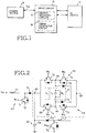
- Fig. 1 is a block diagram of an electroluminescent device and power source according to an embodiment of this invention;
- Fig. 2 is a schematic diagram of the energy recovery circuit and EL device of Fig. 1 according to an embodiment of this invention;
- Fig. 3 is a chart of panel voltage over the charging and discharging phases of the power cycle using the energy recovery circuit of Fig. 2;
- Fig. 4 is a timing diagram showing transistor states for energy recovery circuit components at various times during the power cycle; and
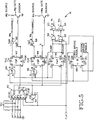
- Fig. 5 is a schematic diagram of a timing generator circuit for controlling switching within the energy recovery circuit of Fig. 2.
- Fig. 1 shows a block diagram of an electroluminescent ("EL")
device 10,power source 12 and drivecircuit 14 according to an embodiment of this invention. TheEL device 10 is an electroluminescent panel, electroluminescent lamp or other electroluminescent lighting device.Such EL devices 10 are capacitive in nature. Thepower source 12 supplies a dc input voltage signal, Vin, to thedrive circuit 14. Thedrive circuit 14 receives the voltage signal and drives theEL device 10 to alternating high and low potentials at reversing polarity to generate light. - The
drive circuit 14 includes anenergy recovery circuit 16 and atiming generator circuit 18. Theenergy recovery circuit 14 receives the input voltage signal, Vin, and generates an alternating polarity power input signal to theEL device 10 based upon timing signals provided by thetiming generator circuit 18. For each polarity of the power cycle there is a charging phase and discharging phase. TheEL device 10 is charged to a high potential at one polarity, then discharged to a low potential. The polarity then reverses and thedevice 10 is charged to a high potential at the opposite polarity. Thedevice 10 then discharges to a low potential and the polarity again reverses to begin a new power cycle. - The
EL device 10 repeatedly is charging and discharging during operation. During a charging phase, a portion of input energy is absorbed by thedevice 10, a portion is dissipated as heat and a portion is converted to light. During a discharging phase, the previously absorbed energy is released. The function of the power recovery circuit is to absorb a portion of the released energy for re-use during a subsequent charging phase. The more energy recovered in this way, the more efficient are theEL panel 10 andrelated drive circuitry 14. By recovering energy for-reuse, the net input frompower source 12 is reduced, thereby reducing the power consumption of theEL device 10. - Fig. 2 shows a schematic diagram of the
energy recovery circuit 16 withEL device 10 according to a preferred embodiment of this invention. TheEL device 10 is represented electrically by its characteristic load capacitance, CL, and load resistance, RL. During an energy charging phase, thedevice 10 receives energy. A portion of the received energy is stored in thedevice 10 due to its load capacitance CL. Another portion is converted to light. - During an energy discharging phase, capacitive energy stored in the device 10 (e.g., CL) is discharged. A portion of this discharged energy is dissipated as heat via the device's load resistance, RL. The function of the
energy recovery circuit 16, however, is to re-absorb a portion of this discharged capacitive energy, thereby reducing the portion dissipated as heat. Such re-absorbed energy then is re-applied to thedevice 10 during a subsequent charging phase. As a result, the power drawn from thesource 12 to power theEL device 10 is reduced. TheEL device 10, in effect, becomes more efficient when coupled with theenergy recovery circuit 16. - The
energy recovery circuit 16 includes a chargingpump stage 20, arecovery pump stage 22, and abridge stage 24. The chargingpump stage 20 pumps energy frompower source 12 into theEL device 10 during a charging phase. Therecovery pump stage 22 absorbs load capacitance CL discharge energy during the discharging phase and inputs a portion of that absorbed energy back into theEL device 10 during a subsequent charging phase. Thebridge stage 24 defines a power cycle controlling the polarity of energy input to theEL device 10 and the charging and discharging phase transitions. - The charging
pump stage 20 includes an inductor L₁, diode D₁, and switching transistor T₁. The inductor L₁ receives the dc voltage input signal Vin frompower source 12. Energy then is pumped from the inductor L₁ to theEL device 10 by transistor T₁. By switching transistor T₁ on and off, the inductor L₁ is cyclically loaded and released. Diode D₁ prevents current from traveling back into thebooster stage 20 during discharging phases. - The
recovery pump stage 22 includes an inductor L₂, a switching transistor T₆, a diode D₄, and a recovery capacitor CR. During a discharge phase of the power cycle, theEL device 10 load capacitance CL is discharged. A portion of this discharged energy is dissipated by load resistance RL. A significant portion, however, flows to inductor L₂. The energy is pumped from inductor L₂ to a recovery capacitor, CR, for storage. Transistor T₆ periodically switches on and off during this discharge phase to pump the energy through the inductor L₂ into capacitor CR. During the next charging phase of the power cycle, the recovery capacitor, CR, discharges its energy to flow back into theEL device 10. Thus, during a charging phase, theEL device 10 receives energy from both the charging pump stage 20 (e.g., inductor L₁) and the recovery pump stage 22 (e.g., capacitor CR). - The
bridge stage 24 includes afirst bridge 26, a second bridge 28 and diodes D₂ and D₃. When thefirst bridge 26 is active, second bridge 28 is inactive. Similarly, when second bridge 28 is active,first bridge 26 is inactive. Whenfirst bridge 26 is active, energy flow into theEL device 10 is at one polarity. When second bridge 28 is active, energy flow intoEL device 10 is at the opposite polarity. When neitherbridge 26, 28 is active, the EL device is isolated. Thefirst bridge 26 is formed by transistors T₂ and T₃. The second bridge 28 is formed by transistors T₄ and T₅. - In one embodiment the switching devices T₁ - T₆ are formed by power FETs having intrinsic body diodes. These body diodes are shown across the source and drain of each transistor in Fig. 2. The body diodes of transistors T₃ and T₅ provide a return path for EL device discharge current while the switching transistors T₂-T₅ of the first and
second bridges 26, 28 are off. In an alternate embodiment only the transistors T₃ and T₅ have body diodes. In still another embodiment, transistors T₃ and T₅ do not have body diodes, but instead have high efficiency schottky diodes across their respective source and drain contacts. - Fig. 3 shows the voltage signal, VL, across the
EL device 10 over the power cycle. The power cycle includes a chargingphase 32 and a dischargingphase 34 at a first polarity, followed by a chargingphase 36 and dischargingphase 38 at the opposite polarity. Fig. 4 shows a timing diagram of the switching transistor T₁-T₆ states for the charging and discharging phases 32-38. - Charging and discharging phases of the EL device are defined by toggling
bridge 26 or 28 switching transistors. During a charging phase at one polarity, transistors T₂ and T₃ are on and transistors T₄ and T₅ are off. During the discharging phase of the same polarity, transistors T₂, T₃, T₄ and T₅ are off. During the subsequent charging phase at the opposite polarity, transistors T₂ and T₃ are off and transistors T₄ and T₅ are on. During the discharging phase of such opposite polarity, transistors T₂, T₃, T₄ and T₅ are off. When transistors T₂ through T₅ are off, theload device 10 is isolated. When transistor T₆ switches on a low potential forward biases the diode D₂ or D₃ (depending on the polarity) providing a discharge path. Theload 10 discharges through diode D₂ or D₃ while transistor T₆ is on. The body diodes of transistors T₃ and T₅ provide the return path for the discharge current. By switching transistor T₆ on and off, the load capacitance CL discharges to inductor L₂ in small energy portions. - The charging
phase 32 at a first polarity (e.g., positive) begins at time t₀. At time t₀ signal M₁ becomes active cyclically switching the transistor T1 on and off. While on, inductor L₁ passes a small portion of the input voltage Vin energy from thepower source 12 to theload 10 viabridge 26 or 28 to develop a load voltage, VL. A portion of the incoming energy is stored in the load capacitance CL. Another portion is converted to light. - As shown in Fig. 4, signals M₂ and M₅ are low and signals M₃ and M₄ are high during the
charging phase 32. Thus, thefirst bridge 26 is active. Transistor T₃ putsnode 40 near ground potential and transistor T₂ putsnode 42 at a high potential. The incoming energy is pumped through thefirst bridge 26 to theEL panel 10 to build the load voltage VL to a high potential at a first polarity (e.g., positive). Fig. 3 shows the incremental rise in voltage, VL, across theEL load 10 duringphase 32. Each step-like increase in voltage, VL, corresponds to the energy pumped from inductor L₁ during one switching period of signal M₁. - The shape of signal VL during the
charging phase 32 is determined by the inductor L₁ timing constant, the signal M₁ frequency, and the load capacitance CL timing constant. The step-like increments in VL are determined by the inductor L₁ timing constant and the signal M₁ frequency. - The discharging
phase 34 begins at time t₁. During the dischargingphase 34, signal M₁ is kept low preventing energy from flowing from the chargingpump stage 20 to theEL panel 10. Signal M₂ switches high and signal M₃ switches low so that transistors T₂-T₅ are off isolating theload 10. Whenever T₆ switches on, diode D₂ is forward biased forcing the panel to discharge toward a lower potential. The run-off current enters inductor L₂. Transistor T₆ pumps the current from the inductor L₂ through diode D₄ charging the recovery capacitor CR. Fig. 3 shows the incremental lowering of voltage across theEL device 10 duringphase 34 due to the pumping action. Fig. 4 shows the switching of transistor T₆ triggering the pumping action. The shape and step-like decrements in VL are determined by the inductor L₁ timing constant, the signal M₁ frequency and the load capacitance CL timing constant. - The
next charging phase 36 begins at time t₂. During thecharging phase 36, signal M₆ is held low keeping the transistor T₆ off so no more energy flows through the inductor L₂ into capacitor CR. Also, signal M₄ is switched low and signal M₅ is switched high so that transistors T₄ and T₅ are on and transistors T₂ and T₃ are off. This activates the second bridge 28 jumpingnode 40 to a first potential as capacitor CR discharges. Diode D₄ keeps the discharge energy from flowing as current back toward inductor L₂. The current flows tonode 44 and into theEL panel 10.Node 44 increases its voltage potential magnitude as energy is received from both the inductor L₁ and the capacitor CR. - With the second bridge 28 active, the energy flow from
node 44 tonodes puts node 40 at a high potential andnode 42 at a low potential. Thus, the energy fromnode 44 flows in the reverse direction to theEL panel 10 compared with the flow during thecharging phase 32. TheEL panel 10 is brought to a high potential, VL, at the opposite polarity (e.g., negative). Fig. 3 shows the incremental rise in voltage duringphase 36 due to the pumping action. Fig. 4 shows the switching of transistor T₁ triggering the pumping action. The shape and step-like decrements in signal VL are determined by the inductor L₁ timing constant, the signal M₁ frequency and the load capacitance CL timing constant. - The next discharging
phase 38 begins at time t₃. During the dischargingphase 38, signal M₁ is kept low preventing energy from flowing from the chargingpump stage 20 to theEL panel 10. Signal M₄ switches high and signal M₅ switches low so that transistors T₂-T₅ are off isolating theload 10. Whenever T₆ switches on, diode D₃ is forward biased forcing the panel to discharge toward a lower potential. The run-off current enters inductor L₂. Transistor T₆ pumps the current from the inductor L₂ through diode D₄ charging the recovery capacitor CR. Fig. 3 shows the incremental lowering of voltage magnitude across theEL device 10 duringphase 38 due to the pumping action. Fig. 4 shows the switching of transistor T₆ triggering the pumping action. The shape and step-like decrements in VL are determined by the inductor L₁ timing constant, the signal M₁ frequency and the load capacitance CL timing constant. - The next power cycle then begins with a charging
phase 32. Signal M₆ is held low keeping the transistor T₆ off so no more energy flows through the inductor L₂ into capacitor CR. Also, signal M₂ is switched low and signal M₃ is switched high so that transistors T₂ and T₃ are on and transistors T₄ and T₅ are off. This activates thefirst bridge 26 jumpingnode 42 to a first potential as capacitor CR discharges. Diode D₄ keeps the discharge energy from flowing as current back toward inductor L₂. The current flows tonode 44 and into theEL panel 10.Node 44 increases its voltage potential magnitude as energy is received from both the inductor L₁ and the capacitor CR. - As previously described signal M₁ switches transistor T₁ on and off to pump energy from the inductor L₁ to the EL panel. Energy flow from
node 44 tonodes puts node 42 at a high potential andnode 40 at a low potential. Thus, the energy fromnode 44 flows in the reverse direction to theEL panel 10 compared with the flow during chargingphase 36. TheEL panel 10 thus is brought to a high potential, VL, at the first polarity (e.g., positive). - The power cycle repeats with energy being pumped to the
EL panel 10 during chargingphases EL panel 10 during discharge phases 34, 38. During each charging phase, energy is supplied from thepower source 12 via chargingpump stage 20 and from the recovery capacitor CR of therecovery pump stage 22. - Each incremental step in voltage, VL, during charging
phases phases - Fig. 5 shows a schematic diagram of a
circuit 18 embodiment for generating the timing signals M₁ through M₆ of Fig. 4. Thecircuit 18 includes several D flip-flops counter 50 and several NAND gates 52-64 andinverters counter 50 to transition every X number of clock pulses. X defines the number of T₁ switches during acharging phase - Every
counter 50 transition marks a phase change (e.g.,phase 32 to phase 34) in the power cycle. Flip-flop 48 is toggled every two counter transitions to enable the first bridge (transistors T₂, T₃) or the second bridge (transistors T₄, T₅). Flip-flop 46 is toggled every counter transition to switch between a charging phase and a discharging phase. Flip-flop 42 is driven by flip-flop 48 when the first bridge is active. Flip-flop 44 is driven by flip-flop 48 when the second bridge is active. - Although the embodiment for the
timing generator circuit 18 is depicted with discrete components, in a preferred embodiment, timing circuitry is formed on an integrated circuit. Any of many alternative logic formations are implemented on the IC to achieve the timing pattern of Fig. 4. - For a best mode embodiment, the
energy recovery circuit 16 andtiming generator circuit 18 are formed on a common integrated circuit designed to minimize parasitic effects. In particular, parasitic capacitances and inductances attributable to high frequency switching action are greatly minimized by a common IC tuned for a specific switching frequency range. Note that low-profile inductors and capacitors are formed off-chip. - For a given
EL panel 10energy recovery circuit 16 values are selected based on a desired switching frequency range. Different values are preferred for different frequency ranges to best tune out parasitic effects of the transistors T₁ to T₆. - In one embodiment inductors L₁ and L₂ are formed by discrete inductive coils or other inductive structures. In one embodiment capacitor CR is formed by a capacitor or other capacitive structure. In one embodiment the diodes D₁-D₄ are formed by diodes or other diode-like structures (e.g., transistor wired as diode). In an IC embodiment the diodes preferably are formed by diode or diode-like structures integral to the IC. In one embodiment switches T₁-T₆ are FET transistors operated as switching devices, although other switching transistors or switching devices also may be used. In an IC embodiment devices T₁-T₆ are switching structures integral to the IC chip. Such switching structures may be transitive structures or other switching structures. The structures implemented for
circuit 16 components also may vary depending on the IC technology. - In the preferred embodiment, pumping occurs during the entire charging phase or discharging phase. In alternate embodiments, however, pumping may occur over a portion of the charging or discharging phase. In various embodiments, the number of switching periods in a charging phase may be the same or differ from the number of switching periods during a discharging phase.
- This invention addresses the problem of power inefficiencies in EL devices. To make EL device usage more efficient, energy is recovered from the EL device during discharge. As EL devices are capacitive in nature, such devices are powered by charging the device to a high potential, then discharging the device to a low potential. Only a small portion of such energy input to the device, however, is used to generate light. It is therefore desirable to recover some of the energy during discharge and re-use to charge the EL device during a subsequent charging period.
- While prior solutions have performed energy recovery using resonant tank circuits, the solution of this invention is to provide a switching scheme for pumping energy into and out of the EL device. By using a switching scheme energy is moved in smaller units. Conventional resonant tank circuits absorb discharge energy and re-enter the energy into the EL device based upon the timing constants of the capacitive and inductive components of the EL device and resonant tank. Such components are comparatively larger than for the inventive circuit making the resonant tank approach impractical for implementation in small hand-held devices.
- The switching scheme of this approach uses transistors to define a power cycle, trigger charging and discharging phases, and pump energy into and out of the EL device. The pump stages include inductors which pump energy in smaller amounts than the EL load capacitance freely discharges.
- One advantageous effect of the energy recovery circuit of this invention is that the switching action used for pumping energy into and out of the EL device allows smaller units of energy to be controlled. The switching scheme allows smaller components to achieve energy recovery, as compared to components required by conventional resonant tank energy recovery circuits. An effect of the smaller components is that the energy recovery circuit of this invention is easily implemented in very small devices.
- Another advantageous effect of the energy recovery circuit of this invention is a reduced power consumption. Reduced power consumption is particularly beneficial for EL panels used with portable computing devices. As the panel is powered by battery, it operates for a longer time period before the battery needs to be recharged.
- Another advantageous effect of the energy recovery circuit is that less heat is generated in powering an EL device. Thus the need to provide cooling mechanisms is reduced. Reduced cooling requirements means a lighter weight panel may be achieved and that the panel can be used in higher temperature environments.
- Another advantageous effect of the energy recovery circuit is that effective steady state currents in the EL drive circuit are reduced.
- Although a preferred embodiment of the invention has been illustrated and described, various alternatives, modifications and equivalents may be used. Therefore, the foregoing description should not be taken as limiting the scope of the inventions which are defined by the appended claims.
Claims (10)
- An energy recovery circuit (16) for powering an EL device (10), comprising:
a first inductor (L₁) coupled to the EL device (10) and receiving a voltage signal (Vin) from a power source (12), the first inductor (L₁) storing energy from the power source (12);
a first switch (T₁) coupled to the first inductor (L₁) for pumping energy from the first inductor (L₁) to the EL device (10) to charge the EL device (10);
a second inductor (L₂) coupled to the EL device (10) and receiving EL device discharge energy;
a second switch (T₆) coupled to the second inductor (L₂);
a first capacitor (CR) coupled to the second inductor (L₂) and the EL device (10);
the second switch (T₆) for pumping EL device discharge energy from the second inductor (L₂) to the first capacitor (CR) while the EL device (10) is discharging;
the first capacitor (CR) storing pumped discharge energy, then releasing the stored discharge energy into the EL device (10) to charge the EL device (10). - The energy recovery circuit of claim 1, further comprising:
a first bridge (26) and a second bridge (28) formed across the EL device (10), the first inductor (L₁) coupled to the EL device (10) via the first bridge (26) and second bridge (28), the first bridge and second bridge receiving timing signals for defining a power cycle, the power cycle having a charging phase and discharging phase at one polarity followed by a charging phase and a discharging phase at an opposite polarity; and
wherein the first switch (T₁) pumps energy from the first inductor (L₁) to the EL device (10) and the first capacitor (CR) releases discharge energy into the EL device during charging phases of the power cycle; and
wherein the second switch (T₆) pumps EL device discharge energy from the second inductor (L₂) to the first capacitor (CR) during discharging phases of the power cycle. - The energy recovery circuit of claim 2, in which the first bridge (26) comprises a first transistor (T₂) and a second transistor (T₃) coupled to the EL device (10) as an electrical bridge; and in which the second bridge (28) comprises a third transistor (T₄) and a fourth transistor (T₅) coupled to the EL device (10) as an electrical bridge.
- An energy recovery circuit (16) for powering an EL device (10), comprising:
a first stage (20) for receiving a voltage signal (Vin) from a power source (12), the first stage comprising a first inductor (L1) and a first switch (T₁), the first inductor receiving the voltage signal (Vin) and storing energy, the first switch pumping energy from the first inductor to the EL device during charging phases of an EL device power cycle;
a first bridge (26) and a second bridge (28) formed across the EL device and coupled to the first stage (20), the first bridge and second bridge receiving timing signals for defining the EL device power cycle, the power cycle having a charging phase (32) and discharging phase (34) at one polarity followed by a charging phase (36) and a discharging phase (38) at an opposite polarity;
a second stage (22) for receiving EL device discharge energy, the second stage coupled to the first bridge and second bridge and to the EL device, the second stage (22) comprising a second inductor (L₂), a second switch (T₆) and a first capacitor (CR), the second inductor (L₂) coupled to the EL device and receiving EL device discharge energy, the second switch (T₆) pumping EL device discharge energy from the second inductor (L₂) to the first capacitor during discharging phases (34, 38) of the power cycle, the first capacitor (CR) storing the pumped discharge energy during discharging phases (34, 38) and releasing the stored energy into the EL device via the first bridge (26) or second bridge (28) during a charging phase (32, 36). - The energy recovery circuit of claim 4, in which the first bridge (26) comprises a first transistor (T₂) and a second transistor (T₃) coupled to the EL device (10) as an electrical bridge; and in which the second bridge (28) comprises a third transistor (T₄) and a fourth transistor (T₅) coupled to the EL device (10) as an electrical bridge.
- The energy circuit of claim 5 in which respective first, second, third and fourth transistors (T₂, T₃, T₄, T₅) receive respective first, second, third and fourth timing signals (M₂, M₃, M₄, M₅) for defining the EL device power cycle.
- A method of charging and discharging an EL device (10) during a power cycle, comprising the steps of:
charging the EL device (10) by transferring a sequence of discrete energy portions from a power source (12) to the EL device to incrementally accumulate a high energy potential (VL) across the EL device; and
discharging the EL device by capturing a sequence of discrete discharge energy portions from the EL device at a capacitor (CR); and
wherein the step of charging further comprises discharging the capacitor into the EL device. - The method of claim 7 in which the step of transferring comprises the steps of:
storing energy from the power source (12) at a first inductor (L₁);
releasing the stored energy to the EL device (10); and
repeating the storing and releasing steps during a charging phase (32, 36) of the power cycle. - The method of claim 7 in which the step of capturing comprises the steps of:
storing a discharge energy portion from the EL device at a second inductor (L₂);
releasing the stored discharge energy portion to the capacitor (CR); and
repeating the storing and releasing steps during a discharging phase (34, 38) of the power cycle. - The method of claim 8, in which a first bridge (26) and a second bridge (28) are formed across the EL device (10), the first inductor (L₁) coupled to the EL device via the first bridge and second bridge, and further comprising the step of:
receiving timing signals (M₂, M₃, M₄, M₅) at the first bridge (26) and second bridge (28) for defining a power cycle, the power cycle having a charging phase (32) and discharging phase (34) at one polarity followed by a charging phase (36) and a discharging phase (38) at an opposite polarity.
Applications Claiming Priority (2)
| Application Number | Priority Date | Filing Date | Title |
|---|---|---|---|
| US296194 | 1994-08-24 | ||
| US08/296,194 US5559402A (en) | 1994-08-24 | 1994-08-24 | Power circuit with energy recovery for driving an electroluminescent device |
Publications (2)
| Publication Number | Publication Date |
|---|---|
| EP0699015A1 true EP0699015A1 (en) | 1996-02-28 |
| EP0699015B1 EP0699015B1 (en) | 2000-06-14 |
Family
ID=23141003
Family Applications (1)
| Application Number | Title | Priority Date | Filing Date |
|---|---|---|---|
| EP95305109A Expired - Lifetime EP0699015B1 (en) | 1994-08-24 | 1995-07-21 | Power circuit with energy recovery for driving an electroluminescent device |
Country Status (4)
| Country | Link |
|---|---|
| US (1) | US5559402A (en) |
| EP (1) | EP0699015B1 (en) |
| JP (1) | JP3524645B2 (en) |
| DE (1) | DE69517477T2 (en) |
Cited By (15)
| Publication number | Priority date | Publication date | Assignee | Title |
|---|---|---|---|---|
| EP0782373A1 (en) * | 1995-12-26 | 1997-07-02 | Pioneer Electronic Corporation | Method and apparatus for driving capacitive light emitting device |
| WO1998057524A1 (en) * | 1997-06-09 | 1998-12-17 | Telefonaktiebolaget Lm Ericsson | An inverter circuit for illuminating an electroluminescent lamp |
| EP0899989A2 (en) * | 1997-08-26 | 1999-03-03 | STMicroelectronics, Inc. | Method and apparatus for driving an electroluminescent lamp |
| FR2779884A1 (en) * | 1998-06-16 | 1999-12-17 | Magneti Marelli France | Electronic power supply device for electroluminescent panel in automobiles |
| US6157138A (en) * | 1998-12-31 | 2000-12-05 | Telefonaktiebolaget Lm Ericsson | Apparatus for illuminating an electroluminescent lamp that preserves battery power |
| EP1106037A1 (en) * | 1998-07-15 | 2001-06-13 | Durel Corporation | Power supply including a voltage boost for operating an el lamp from a battery |
| US6376934B1 (en) | 1999-08-18 | 2002-04-23 | Sipex Corporation | Voltage waveform generator |
| WO2002037900A2 (en) * | 2000-11-02 | 2002-05-10 | Koninklijke Philips Electronics N.V. | Energy-recovering electroluminescent panel supply/driver circuit |
| GB2372646A (en) * | 2001-02-26 | 2002-08-28 | Cambridge Consultants | Power supply circuit for an electroluminescent lamp |
| US6781423B1 (en) | 2003-07-04 | 2004-08-24 | Dialog Semiconductor Gmbh | High-voltage interface and driver control circuit |
| GB2405270A (en) * | 2003-08-22 | 2005-02-23 | Pelikon Ltd | Control circuit for capacitive load |
| WO2010088954A1 (en) * | 2009-02-04 | 2010-08-12 | Osram Gesellschaft mit beschränkter Haftung | Circuit configuration and method for operating an electroluminescent film |
| EP2469981A1 (en) * | 2010-12-27 | 2012-06-27 | NK Works Co., Ltd. | LED drive circuit |
| US8698978B2 (en) | 2004-06-11 | 2014-04-15 | Mflex Uk Limited | Electroluminescent displays |
| WO2018075742A1 (en) * | 2016-10-20 | 2018-04-26 | Lawrence Livermore National Security, Llc | Multiple pulse charge transfer for capacitive deionization of a fluid |
Families Citing this family (37)
| Publication number | Priority date | Publication date | Assignee | Title |
|---|---|---|---|---|
| US5302966A (en) * | 1992-06-02 | 1994-04-12 | David Sarnoff Research Center, Inc. | Active matrix electroluminescent display and method of operation |
| JP2755201B2 (en) * | 1994-09-28 | 1998-05-20 | 日本電気株式会社 | Drive circuit for plasma display panel |
| US5568016A (en) * | 1994-10-18 | 1996-10-22 | Norand Corporation | Power supply for an electroluminescent panel or the like |
| JP2735014B2 (en) * | 1994-12-07 | 1998-04-02 | 日本電気株式会社 | Display panel drive circuit |
| JP3241577B2 (en) * | 1995-11-24 | 2001-12-25 | 日本電気株式会社 | Display panel drive circuit |
| US5789870A (en) * | 1996-05-06 | 1998-08-04 | Durel Corporation | Low noise inverter for EL lamp |
| US6108000A (en) * | 1997-03-05 | 2000-08-22 | Microdisplay Corporation | Resonant driver apparatus and method |
| JP3667928B2 (en) * | 1997-03-18 | 2005-07-06 | パイオニア株式会社 | EL element driving apparatus and driving method |
| US5892395A (en) * | 1997-05-02 | 1999-04-06 | Motorola, Inc. | Method and apparatus for efficient signal power amplification |
| KR100277407B1 (en) * | 1998-06-30 | 2001-01-15 | 전주범 | Power recovery method of plasma display panel television and its circuit |
| JP3395760B2 (en) * | 1999-06-01 | 2003-04-14 | セイコーエプソン株式会社 | Voltage generation method, electro-optical device, and electronic apparatus |
| KR100566813B1 (en) * | 2000-02-03 | 2006-04-03 | 엘지.필립스 엘시디 주식회사 | Circuit for Electro Luminescence Cell |
| US6448950B1 (en) | 2000-02-16 | 2002-09-10 | Ifire Technology Inc. | Energy efficient resonant switching electroluminescent display driver |
| US6867755B2 (en) * | 2000-04-28 | 2005-03-15 | Yazaki Corporation | Device and method for driving EL device |
| KR100515745B1 (en) * | 2000-11-09 | 2005-09-21 | 엘지전자 주식회사 | Energy recovering circuit with boosting voltage-up and energy efficient method using the same |
| EP1336326A4 (en) * | 2000-11-22 | 2004-04-14 | Fusion Uv Sys Inc | Ultraviolet lamp power supply and method for operating at high power/reduced cooling using cycling |
| KR100400007B1 (en) * | 2001-06-22 | 2003-09-29 | 삼성전자주식회사 | Apparatus and method for improving power recovery rate of a plasma display panel driver |
| JP4080775B2 (en) * | 2001-07-06 | 2008-04-23 | セイコーインスツル株式会社 | EL drive circuit, control method for EL drive circuit, and electronic apparatus |
| US6819308B2 (en) | 2001-12-26 | 2004-11-16 | Ifire Technology, Inc. | Energy efficient grey scale driver for electroluminescent displays |
| EP1488667A1 (en) * | 2002-03-19 | 2004-12-22 | Koninklijke Philips Electronics N.V. | Driver circuit for an electroluminescent lamp |
| KR100454029B1 (en) * | 2002-06-12 | 2004-10-20 | 삼성에스디아이 주식회사 | Circuit for energy controlling of switched mode power supply for plasma display panel and method thereof |
| CA2391681A1 (en) * | 2002-06-26 | 2003-12-26 | Star Headlight & Lantern Co. Of Canada Ltd. | Solid-state warning light with microprocessor controlled excitation circuit |
| JP2005003836A (en) * | 2003-06-11 | 2005-01-06 | Tohoku Pioneer Corp | Driving device of light emitting display panel and driving method |
| DE10356515A1 (en) * | 2003-12-03 | 2005-07-14 | Siemens Ag | drive system |
| US20060033680A1 (en) * | 2004-08-11 | 2006-02-16 | Lg Electronics Inc. | Plasma display apparatus including an energy recovery circuit |
| JP5011478B2 (en) * | 2005-08-22 | 2012-08-29 | 株式会社ジャパンディスプレイイースト | Display device |
| TWI277929B (en) * | 2005-10-19 | 2007-04-01 | Chunghwa Picture Tubes Ltd | Method and apparatus for driving plasma display panel to improve characteristic thereof using multi-discharge phenomenon |
| KR101325979B1 (en) * | 2008-12-24 | 2013-11-07 | 엘지디스플레이 주식회사 | Power supply unit for organic electroluminescent display device |
| JP2012033409A (en) * | 2010-07-30 | 2012-02-16 | Origin Electric Co Ltd | Reversed-polarity pulse generating circuit for dc plasma, and dc plasma power supply device |
| BR112013022629A2 (en) * | 2011-03-07 | 2016-12-06 | Koninkl Philips Nv | electroluminescent device, lighting fixture and system |
| US9357596B2 (en) * | 2011-06-30 | 2016-05-31 | Nokia Technologies Oy | Drivers for loads such as light emitting diodes |
| US20130200815A1 (en) * | 2012-02-06 | 2013-08-08 | David Schie | Energy storage means for last gasp / impedance limited applications |
| GB201309282D0 (en) | 2013-05-23 | 2013-07-10 | Shimadzu Corp | Circuit for generating a voltage waveform |
| US9077284B2 (en) | 2013-06-26 | 2015-07-07 | Werlatone, Inc. | Absorptive RF rectifier circuit |
| US20190067753A1 (en) * | 2016-02-24 | 2019-02-28 | The Regents Of The University Of Colorado, A Body Corporate | Heterogeneous energy storage system and method of controlling a heterogeneous energy storage system |
| US11146267B1 (en) | 2020-11-30 | 2021-10-12 | Stmicroelectronics S.R.L. | Charge recovery driver for MEMS mirror with reduced number of tank capacitors |
| US11955900B2 (en) * | 2021-06-30 | 2024-04-09 | Abb Schweiz Ag | Soft turn-off for motor controllers |
Citations (4)
| Publication number | Priority date | Publication date | Assignee | Title |
|---|---|---|---|---|
| EP0359245A2 (en) * | 1988-09-14 | 1990-03-21 | Daichi Co., Ltd | EL operating power supply circuit |
| EP0420518A2 (en) * | 1989-09-25 | 1991-04-03 | Westinghouse Electric Corporation | Power saving drive circuit for TFEL devices |
| EP0487732A1 (en) * | 1990-02-07 | 1992-06-03 | Daichi Co., Ltd | Light-emitting power source circuit |
| EP0508337A2 (en) * | 1991-04-10 | 1992-10-14 | DIEHL GMBH & CO. | Inverter circuit for a capacitive light source |
Family Cites Families (4)
| Publication number | Priority date | Publication date | Assignee | Title |
|---|---|---|---|---|
| US4527096A (en) * | 1984-02-08 | 1985-07-02 | Timex Corporation | Drive circuit for capacitive electroluminescent panels |
| JPH07109798B2 (en) * | 1987-01-06 | 1995-11-22 | シャープ株式会社 | Driving circuit for thin film EL display device |
| US4859911A (en) * | 1987-02-13 | 1989-08-22 | International Business Machines Corporation | Power supply for electroluminescent panel |
| US5227696A (en) * | 1992-04-28 | 1993-07-13 | Westinghouse Electric Corp. | Power saver circuit for TFEL edge emitter device |
-
1994
- 1994-08-24 US US08/296,194 patent/US5559402A/en not_active Expired - Lifetime
-
1995
- 1995-07-21 EP EP95305109A patent/EP0699015B1/en not_active Expired - Lifetime
- 1995-07-21 DE DE69517477T patent/DE69517477T2/en not_active Expired - Fee Related
- 1995-08-23 JP JP21487195A patent/JP3524645B2/en not_active Expired - Fee Related
Patent Citations (4)
| Publication number | Priority date | Publication date | Assignee | Title |
|---|---|---|---|---|
| EP0359245A2 (en) * | 1988-09-14 | 1990-03-21 | Daichi Co., Ltd | EL operating power supply circuit |
| EP0420518A2 (en) * | 1989-09-25 | 1991-04-03 | Westinghouse Electric Corporation | Power saving drive circuit for TFEL devices |
| EP0487732A1 (en) * | 1990-02-07 | 1992-06-03 | Daichi Co., Ltd | Light-emitting power source circuit |
| EP0508337A2 (en) * | 1991-04-10 | 1992-10-14 | DIEHL GMBH & CO. | Inverter circuit for a capacitive light source |
Cited By (26)
| Publication number | Priority date | Publication date | Assignee | Title |
|---|---|---|---|---|
| EP0782373A1 (en) * | 1995-12-26 | 1997-07-02 | Pioneer Electronic Corporation | Method and apparatus for driving capacitive light emitting device |
| WO1998057524A1 (en) * | 1997-06-09 | 1998-12-17 | Telefonaktiebolaget Lm Ericsson | An inverter circuit for illuminating an electroluminescent lamp |
| US6038153A (en) * | 1997-06-09 | 2000-03-14 | Telefonaktiebolaget Lm Ericsson | Inverter circuit for illuminating an electroluminescent lamp |
| EP0899989A2 (en) * | 1997-08-26 | 1999-03-03 | STMicroelectronics, Inc. | Method and apparatus for driving an electroluminescent lamp |
| EP0899989A3 (en) * | 1997-08-26 | 2000-08-02 | STMicroelectronics, Inc. | Method and apparatus for driving an electroluminescent lamp |
| FR2779884A1 (en) * | 1998-06-16 | 1999-12-17 | Magneti Marelli France | Electronic power supply device for electroluminescent panel in automobiles |
| EP1106037A1 (en) * | 1998-07-15 | 2001-06-13 | Durel Corporation | Power supply including a voltage boost for operating an el lamp from a battery |
| EP1106037A4 (en) * | 1998-07-16 | 2005-01-19 | Durel Corp | Power supply including a voltage boost for operating an el lamp from a battery |
| US6157138A (en) * | 1998-12-31 | 2000-12-05 | Telefonaktiebolaget Lm Ericsson | Apparatus for illuminating an electroluminescent lamp that preserves battery power |
| US6376934B1 (en) | 1999-08-18 | 2002-04-23 | Sipex Corporation | Voltage waveform generator |
| WO2002037900A2 (en) * | 2000-11-02 | 2002-05-10 | Koninklijke Philips Electronics N.V. | Energy-recovering electroluminescent panel supply/driver circuit |
| WO2002037900A3 (en) * | 2000-11-02 | 2002-08-01 | Koninkl Philips Electronics Nv | Energy-recovering electroluminescent panel supply/driver circuit |
| WO2002069675A1 (en) * | 2001-02-26 | 2002-09-06 | Pelikon Ltd | Electronic circuits |
| US7102299B2 (en) | 2001-02-26 | 2006-09-05 | Pelikon Limited | Electronic circuits |
| GB2372646A (en) * | 2001-02-26 | 2002-08-28 | Cambridge Consultants | Power supply circuit for an electroluminescent lamp |
| GB2372646B (en) * | 2001-02-26 | 2005-06-22 | Cambridge Consultants | Electronic circuits |
| EP1494354A1 (en) * | 2003-07-04 | 2005-01-05 | Dialog Semiconductor GmbH | High-voltage interface and driver control circuit |
| US6781423B1 (en) | 2003-07-04 | 2004-08-24 | Dialog Semiconductor Gmbh | High-voltage interface and driver control circuit |
| GB2405270B (en) * | 2003-08-22 | 2007-04-11 | Pelikon Ltd | Charge recovery for enhanced transistor drive |
| GB2405270A (en) * | 2003-08-22 | 2005-02-23 | Pelikon Ltd | Control circuit for capacitive load |
| US8698978B2 (en) | 2004-06-11 | 2014-04-15 | Mflex Uk Limited | Electroluminescent displays |
| WO2010088954A1 (en) * | 2009-02-04 | 2010-08-12 | Osram Gesellschaft mit beschränkter Haftung | Circuit configuration and method for operating an electroluminescent film |
| EP2469981A1 (en) * | 2010-12-27 | 2012-06-27 | NK Works Co., Ltd. | LED drive circuit |
| US8810136B2 (en) | 2010-12-27 | 2014-08-19 | Nk Works Co., Ltd. | LED drive circuit |
| WO2018075742A1 (en) * | 2016-10-20 | 2018-04-26 | Lawrence Livermore National Security, Llc | Multiple pulse charge transfer for capacitive deionization of a fluid |
| US10696571B2 (en) | 2016-10-20 | 2020-06-30 | Lawrence Livermore National Security, Llc | Multiple pulse charge transfer for capacitive deionization of a fluid |
Also Published As
| Publication number | Publication date |
|---|---|
| EP0699015B1 (en) | 2000-06-14 |
| JPH0883683A (en) | 1996-03-26 |
| US5559402A (en) | 1996-09-24 |
| DE69517477D1 (en) | 2000-07-20 |
| JP3524645B2 (en) | 2004-05-10 |
| DE69517477T2 (en) | 2000-10-26 |
Similar Documents
| Publication | Publication Date | Title |
|---|---|---|
| EP0699015B1 (en) | Power circuit with energy recovery for driving an electroluminescent device | |
| KR0166432B1 (en) | Method and apparatus for lighting an el element | |
| US6043610A (en) | Battery operated power supply including a low level boost and a high level boost | |
| US6853569B2 (en) | DC to DC converter | |
| US5349269A (en) | Power supply having dual inverters for electroluminescent lamps | |
| US20070052680A1 (en) | Energy recovering circuit with boosting voltage-up and energy efficient method using the same | |
| JP2005505226A (en) | Gate driver device having energy receiving circuit | |
| CN1408140A (en) | Resonant gate drive for synchronous rectifiers | |
| EP0809421A2 (en) | Boost regulator circuit | |
| CN1240036A (en) | Power supply and electronic ballast with low-cost inverter boostrap power source | |
| JP2009176749A (en) | Electronic circuit | |
| US8558525B1 (en) | Power supply circuit and reuse of gate charge | |
| WO2006062936A2 (en) | Single output el driver producing reduced current spikes | |
| US7151344B2 (en) | Electroluminescent driver circuit | |
| US7009823B2 (en) | Energy recovery circuit and energy recovery method using the same | |
| KR100456141B1 (en) | Energy recovering circuit | |
| KR100662466B1 (en) | Energy recovery circuit | |
| JP4233873B2 (en) | Electronic circuit | |
| US7592718B1 (en) | Boosted switch drive with charge transfer | |
| KR20020036240A (en) | Energy Recovering Circuit With Boosting Voltage-Up and It's Driving Method | |
| KR100570965B1 (en) | Energy recovery circuit and its driving method | |
| CN114301276A (en) | Charge pump parasitic capacitance charge recovery circuit | |
| JPH05260730A (en) | Dc-dc converter circuit | |
| KR20050006601A (en) | Energy Recovery Circuit and Driving Method Thereof | |
| JPH11162672A (en) | Lighting device for discharge lamp |
Legal Events
| Date | Code | Title | Description |
|---|---|---|---|
| PUAI | Public reference made under article 153(3) epc to a published international application that has entered the european phase |
Free format text: ORIGINAL CODE: 0009012 |
|
| AK | Designated contracting states |
Kind code of ref document: A1 Designated state(s): DE FR GB |
|
| 17P | Request for examination filed |
Effective date: 19960502 |
|
| 17Q | First examination report despatched |
Effective date: 19980608 |
|
| GRAG | Despatch of communication of intention to grant |
Free format text: ORIGINAL CODE: EPIDOS AGRA |
|
| GRAG | Despatch of communication of intention to grant |
Free format text: ORIGINAL CODE: EPIDOS AGRA |
|
| GRAG | Despatch of communication of intention to grant |
Free format text: ORIGINAL CODE: EPIDOS AGRA |
|
| GRAH | Despatch of communication of intention to grant a patent |
Free format text: ORIGINAL CODE: EPIDOS IGRA |
|
| GRAH | Despatch of communication of intention to grant a patent |
Free format text: ORIGINAL CODE: EPIDOS IGRA |
|
| GRAA | (expected) grant |
Free format text: ORIGINAL CODE: 0009210 |
|
| AK | Designated contracting states |
Kind code of ref document: B1 Designated state(s): DE FR GB |
|
| REF | Corresponds to: |
Ref document number: 69517477 Country of ref document: DE Date of ref document: 20000720 |
|
| ET | Fr: translation filed | ||
| RAP2 | Party data changed (patent owner data changed or rights of a patent transferred) |
Owner name: HEWLETT-PACKARD COMPANY, A DELAWARE CORPORATION |
|
| PLBE | No opposition filed within time limit |
Free format text: ORIGINAL CODE: 0009261 |
|
| STAA | Information on the status of an ep patent application or granted ep patent |
Free format text: STATUS: NO OPPOSITION FILED WITHIN TIME LIMIT |
|
| 26N | No opposition filed | ||
| REG | Reference to a national code |
Ref country code: GB Ref legal event code: IF02 |
|
| REG | Reference to a national code |
Ref country code: GB Ref legal event code: 732E |
|
| REG | Reference to a national code |
Ref country code: FR Ref legal event code: TP |
|
| PGFP | Annual fee paid to national office [announced via postgrant information from national office to epo] |
Ref country code: FR Payment date: 20050718 Year of fee payment: 11 |
|
| REG | Reference to a national code |
Ref country code: FR Ref legal event code: ST Effective date: 20070330 |
|
| PGFP | Annual fee paid to national office [announced via postgrant information from national office to epo] |
Ref country code: DE Payment date: 20070831 Year of fee payment: 13 |
|
| PG25 | Lapsed in a contracting state [announced via postgrant information from national office to epo] |
Ref country code: FR Free format text: LAPSE BECAUSE OF NON-PAYMENT OF DUE FEES Effective date: 20060731 |
|
| PG25 | Lapsed in a contracting state [announced via postgrant information from national office to epo] |
Ref country code: DE Free format text: LAPSE BECAUSE OF NON-PAYMENT OF DUE FEES Effective date: 20090203 |
|
| REG | Reference to a national code |
Ref country code: GB Ref legal event code: 732E Free format text: REGISTERED BETWEEN 20120329 AND 20120404 |
|
| PGFP | Annual fee paid to national office [announced via postgrant information from national office to epo] |
Ref country code: GB Payment date: 20130626 Year of fee payment: 19 |
|
| GBPC | Gb: european patent ceased through non-payment of renewal fee |
Effective date: 20140721 |
|
| PG25 | Lapsed in a contracting state [announced via postgrant information from national office to epo] |
Ref country code: GB Free format text: LAPSE BECAUSE OF NON-PAYMENT OF DUE FEES Effective date: 20140721 |