EP0704851B1 - Byte erasable EEPROM fully compatible with a single power supply flash-EPROM process - Google Patents
Byte erasable EEPROM fully compatible with a single power supply flash-EPROM process Download PDFInfo
- Publication number
- EP0704851B1 EP0704851B1 EP94830459A EP94830459A EP0704851B1 EP 0704851 B1 EP0704851 B1 EP 0704851B1 EP 94830459 A EP94830459 A EP 94830459A EP 94830459 A EP94830459 A EP 94830459A EP 0704851 B1 EP0704851 B1 EP 0704851B1
- Authority
- EP
- European Patent Office
- Prior art keywords
- byte
- cells
- voltage
- flash
- memory
- Prior art date
- Legal status (The legal status is an assumption and is not a legal conclusion. Google has not performed a legal analysis and makes no representation as to the accuracy of the status listed.)
- Expired - Lifetime
Links
Images

Classifications
-
- G—PHYSICS
- G11—INFORMATION STORAGE
- G11C—STATIC STORES
- G11C16/00—Erasable programmable read-only memories
- G11C16/02—Erasable programmable read-only memories electrically programmable
- G11C16/04—Erasable programmable read-only memories electrically programmable using variable threshold transistors, e.g. FAMOS
- G11C16/0408—Erasable programmable read-only memories electrically programmable using variable threshold transistors, e.g. FAMOS comprising cells containing floating gate transistors
- G11C16/0416—Erasable programmable read-only memories electrically programmable using variable threshold transistors, e.g. FAMOS comprising cells containing floating gate transistors comprising cells containing a single floating gate transistor and no select transistor, e.g. UV EPROM
-
- G—PHYSICS
- G11—INFORMATION STORAGE
- G11C—STATIC STORES
- G11C16/00—Erasable programmable read-only memories
- G11C16/02—Erasable programmable read-only memories electrically programmable
- G11C16/06—Auxiliary circuits, e.g. for writing into memory
- G11C16/10—Programming or data input circuits
- G11C16/14—Circuits for erasing electrically, e.g. erase voltage switching circuits
- G11C16/16—Circuits for erasing electrically, e.g. erase voltage switching circuits for erasing blocks, e.g. arrays, words, groups
-
- H—ELECTRICITY
- H10—SEMICONDUCTOR DEVICES; ELECTRIC SOLID-STATE DEVICES NOT OTHERWISE PROVIDED FOR
- H10B—ELECTRONIC MEMORY DEVICES
- H10B69/00—Erasable-and-programmable ROM [EPROM] devices not provided for in groups H10B41/00 - H10B63/00, e.g. ultraviolet erasable-and-programmable ROM [UVEPROM] devices
Definitions
- the present invention relates to the realization on the same chip containing a FLASH-EPROM memory of a byte erasable memory block, that is with the same functionality of a conventional EEPROM memory, in a fully compatible manner with a normal fabrication process of a FLASH-EPROM memory. device with single. supply, without requiring any additional process steps.
- nonvolatile memories based on the principle of trapping an electrical charge in an isolated (floating) gate of a field effect transistor (cell) in order to modify its turn-on threshold, has had and continues to have an extremely important role in the achievement of ever increasing levels of compactness and of speed of integrated systems.
- tunnelling mechanisms may theoretically be exploited also for extracting (discharging) electric charges from the floating gate, that is for "erasing" the cell, even though the voltages that are required must be compatible with the physical-electrical structure of the cell.
- the problem tied to the necessity of biasing the floating gate through its capacitive coupling with a control gate and the semiconducting substrate in order to charge the floating gate and eventually discharge the electrical charge stored therein, has been satisfied by realizing' a capacitive coupling zone between the floating: gate and a drain region of the semiconducting substrate through a thin tunnelling oxide.
- a tunnelling window Through such a tunnelling window, the flow of electrons from the isolated gate and the drain region of the substrate and vice-versa, during an erasing phase and during a programming phase, is obtained through a Flowler-Nordheim tunnelling mechanism by applying a sufficiently high voltage of one sign or of the opposite sign.
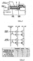
- FIG. 1 A schematic cross section of an EEPROM cell is shown in Fig. 1, while an electrical scheme of an EEPROM memory array is shown in Fig. 2, which contains also a table showing the typical operation voltages.
- the improvement of fabrication technologies has allowed a further reduction of the thickness of the isolation dielectric between a floating gate and the monocrystal silicon. substrate while' reliably ensuring a substantial absence of defects with an average growth thickness of the oxide of about 12nm (120A). This has permitted the development of the so-called FLASH-EPROM or more simply FLASH memories.
- the FLASH memory cell is programmable through a mechanism of injection in the floating gate of hot channel electrons, by biasing the gate (control gate) with a positive voltage sufficiently high (for example in the order of 12V) and the drain with a voltage of about 6V, in order to produce in the channel zone of the monocrystalline silicon substrate of the cell a strong electric field suitable to generate a current of highly energetic (hot) electrons within the silicon, capable of overcoming the potential barrier at the interface with dielectric and of being thereafter attracted toward the floating gate by the electric field.
- a positive voltage sufficiently high for example in the order of 12V
- the drain with a voltage of about 6V
- the electrons that have been injected in the floating gate are able to cross the dielectric according to a Flowler-Nordheim tunnelling mechanism and "discharge" in the source region, during an erasing phase.
- the erasing process of FLASH memories is intrinsically a critical process and is commonly carried out through a succession of pulses of an erasing bias voltage followed by a check until completing the erasing of all the cells of the memory while avoiding to inadvertently bring some of the cells to a depletion state.
- This erasing process engages in a nonnegligeable manner the microprocessor that is called to supervise the erasing process of the FLASH memory.
- each control gate line (wordline) of the memory array overlies (is capacitively coupled) only for a portion of its width, the relative floating gates of the cells of the row, while with a portion of its width the wordline constitutes the gate of as many select transistors, each associated to a respective memory cell of the row.
- wordline control gate line
- a select transistor is associated to each cell, thus making uniform the threshold voltage of all the cells once the erasing of the memory array is performed.
- Block-erasable FLASH-EPROM memories have been proposed to meet these market demands. According to one of these techniques, the possibility of erasing the memory array by blocks is obtained by segmenting the source lines (source diffusions), the use of a further level of metal to define a further order of metal lines to which the portions or segments of source lines are connected through interconnection vias and the realization of an additional decoder for selecting the blocks of the memory array to be erased.
- a .system' of this type is disclosed in US-A-5,289,423.
- US Patent No. 5,033,023 describes a high density EEPROM employing staked gate cells having the ability of being erased and programmed by byte, by employing select lines and a pass-gate transistor for selectively biasing the common source of the cells belonging to a selected byte of a row of matrix cells.
- EP-A-0 405 140 discloses a byte or block erasable array of EEPROM cells wherein cells may be erased singularly for implementing an erasing (and reprogramming) by single byte of the information stored in the memory.
- US patent No. 5,077,691 discloses a FLASH-EEPROM cell array wherein erasure is performed by applying a, negative voltage to the control gate of a row or of a plurality of rows of cells selected for erasing them, the source of which is biased at a comparatively reduced positive voltage with respect to the substrate potential that is normally grounded. Limiting source/substrate voltage during erasing alleviates the risk of breakdowns and of entrapments of charges at the source/substrate interface and related undesired effects.
- the invention provides a way to realize a byte erasable (EEPROM) memory array that employs an array of FLASH-EPROM cells organized in rows and columns and individually addressable (during a programming and a reading phase) through a plurality of wordlines and bitlines, according to a normal architecture of nonvolatile memories.
- EEPROM byte erasable
- the mechanism of programming (writing) the cells remains that of a normal FLASH-EPROM cell, that is injection of hot electrons from the channel region into the floating gate of the cell that takes place in, a zone close to the drain diffusion, while in an erasing phase the mechanism used is the Fowler-Nordheim tunnelling mechanism, that takes place in an overlap zone of the floating gate on the source region of the cell.
- Byte erasability of the memory array is provided by realizing an auxiliary byte selection structure that comprises a byte selection transistor, to a first current terminal of which are connected in common the sources of the cells of a row of the matrix that compose a certain byte, and which has its other current terminal connected to a respective line of a plurality of source biasing lines that are individually selectable by the control circuitry of the memory array.
- the select transistors of the bytes arranged along the same row of the array have their gate driven in common through a respective line of a number of select lines identical to the number of wordlines of the memory array.
- Erasing of a certain byte takes place by biasing, through the byte select transistor connected in series with the sources of the memory cells of the selected byte to be erased, the sources of the cells and the relative wordline (control gate of all the cells of the row containing the byte selected for erasing) with a voltage sufficient to generate a Fowler-Nordheim (FN) tunnelling current of electrons from the floating gate of the cells to their respective source region, while fractioning the applied voltage.
- FN Fowler-Nordheim
- a negative voltage having a value insufficient to cause soft-erasing disturbances on the other unselected memory cells of the same wordline
- a positive , "complementary” voltage is applied to the sources, through the byte, select transistor, that is a positive voltage whose value if related to the tunnelling voltage, is reduced by the absolute value of the negative voltage that is applied to the control gate (multiplied by the capacitive ratio of the floating gate cell structure).
- the drains of the cells may be kept at ground potential or be left floating.
- the voltage applied to a wordline during an erasing phase may be of about -5V while the voltage applied to the sources of the cells of the byte to be erased may be comprised between about 8V and 9V.
- a voltage difference of about 12V-13V is realized while reducing the electrical stress on the other cells of the wordline down to a level that has been found tolerable for the entire period necessary to sequentially erase all the bytes of a wordline.
- a voltage of about 3V may concurrently by applied to all the other (unselected) wordlines.
- programming of the cells may take place by applying the same voltages as in a normal FLASH-EPROM memory.
- a positive voltage of about 12V is applied to the wordline (control gate) while to the drain of the cells to be programmed a positive voltage comprised between 5V and 6V may be applied through the relative bitlines of the memory matrix.
- the common source of the cells of the byte selected for programming is grounded through the byte select transistor, while the sources of all the other cells of the same wordline may advantageously be biased, through their respective byte select transistors, at a positive voltage of an intermediate value, for example of about 3V, to help inhibit soft programming disturbances on unselected cells of the same wordline.
- the byte erasable memory block may employ the same charge pump or voltage muliplier circuits that are required for the operation of the FLASH-EPROM memory and that therefore are already present in the chip.
- the only additional requirement is the integration of a charge pump for generating a negative voltage comprised between about -5V and -8V, in order to "split" the voltage difference that must be imposed between the control gate and the source of the cells selected for erasing, according to the above described manner.
- this additional negative voltage pump has substantially negligeable power requisites, being destined to bias a control gate (wordline).
- the charge pump used for generating the positive voltage for biasing the control gates (wordlines) during programming which may be of about 12V
- the charge pump for generating the positive voltage of about 5V-6V to be applied to the bitlines of the selected cells for programming in case of a single supply device designed for operation with relatively low supply voltage (for example about 3V in the case of battery operable systems) must be designed so as to satisfy the required power requirements.
- the biasing of the drain of a selected cell for programming to a level sufficient to accelerate the channel charge carriers up to sufficiently high kinetic levels (i.e. production. of channel hot electrons) produces a current through the cell's channel of a nonnegligeable value.
- single supply for example a 5 ⁇ 10%V or a 3.3 ⁇ 10%V device
- such a power requisite may be satisfied directly from the supply.
- considerations tied to the voltage drops along the current path may impose to limit the programming to few bits at the time, for example to only two bits at the time.
- the resistance of the programming current path for example to the "farthest" cell of an octet of cells constituting a selected byte for programming, may have 'reached one to several hundreds ohms and the voltage drop, in consideration of the relatively high current (in the vicinity of about 100-500 ⁇ A per cell), could become excessive if all the cells of the byte are written in parallel.
- the EEPROM memory block may offer an "ERASE ALL" function, in a completely compatible way.
- the increased power needed for implementing an erase all function of the EEPROM memory block may be provided by exploiting either the supply or the high power.
- charge pump circuit destined to generate the voltage of about 5V-6V necessary for biasing the drain during the writing of the cells for biasing through the respective byte select transistors the sources and incrementing the absolute value of the negative voltage for biasing the wordlines from the value of about -5V used for byte erasing to a value of about -8V, thus ensuring also during an ERASE ALL phase a voltage difference of about 12V between the source and the control gate of the memory cells.
- each select line to which the gates of all the byte select transistors of the bytes arranged along the same row of FLASH-EPROM memory cells are connected is always selected together with the respective wordline of the row of memory cells, during any phase of operation of the memory block.
- the wordline and to the respective select line that may be logically selected by a single decoder different voltages will be applied during the various phases of operation of the memory.
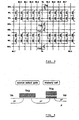
- FIG. 3 The architecture of an EEPROM memory block of the invention, employing a matrix of FLASH-EPROM cells, is depicted in Fig. 3.
- the portion of the array of Fig. 3 shows four bytes, each of a 8 bits, for a matrix that. may have relatively large dimensions.
- Four wordlines (WL) and eight bitlines (BL0 ... BL7) of the four bytes shown are identified in the circuit diagram.
- the entire array would be an expansion in the two "orthogonal" directions of wordlines and of bitlines, respectively, of the portion depicted in Fig. 3.
- the particular unit of information (byte) that is individually erasable (and programmable), may also be composed by a lesser or a larger number of bits and be referred to as for instance a "word” etc..
- the expression "byte” is not to be taken as identifying a unit of information necessarily of eight bits. On the contrary, it may also be composed of a number of bits equal or smaller than eight.
- the single FLASH-EPROM memory cells are identified by the relative graphical symbol of a transistor having a double gate.
- the drains of the cells arranged along each column of the matrix are connected by pairs of adjacents cells to a respective bitline, through drain contacts.
- the sources of all the eight cells of a row that form a byte are connected in common and to a first current terminal of a byte select transistor (Tb1, Tb2, Tb3 and Tb4).
- the source node typically common to all the cells of the matrix
- the source diffusions are in the forms of segments, each "segment" pertaining to the cells belonging to a certain byte, along a certain wordline (row) of the matrix.
- a byte select transistor is formed, through which the source common to the (eight) cells of the byte may be biased at a certain voltage, during the different phases of operation of the memory.
- a first current terminal of each byte select transistor (Tb1 ... Tb4) is connected to the source diffusion of the cells of the respective byte while the other current terminal is connected, through a contact, to a source biasing line Vs.
- To the same source biasing line Vs may be connected the relative current terminals of all the byte select transistors (Tb1, Tb2, Tb3, Tb4 ...) pertaining to all the bytes that are arranged along a column-wise direction of the memory array.
- the source biasing lines Vs are individually selectable by a suitable decoder, made according to common techniques.
- connection of the byte select transistors to a respective source biasing line Vs may be realized through a single source contact (C2) for every two adjacent bytes along a column-wise direction.
- the resistance of the conductive path through the cell of a selected bit may be reduced and differences among the paths of the various cells that compose a certain byte may be minimized by realizing the byte select transistor at a middle position in relation to the number of cells that form the byte and realizing the byte select transistor with an incremented size (width) as compared with the width of the floating gate cells.
- the byte select transistor has a width that is a multiple of the width of the cells by a factor equivalent to the number of bits of the bytes.
- the byte select transistors Tb1 ... Tb4 should be made. about eight times larger than the memory cells.
- each memory cell coupled with a byte select transistors in series with its source is schematically depicted in Fig. 4.
- the source biasing voltage Vs is applied through a source contact to a drain (n + ) region of the byte select transistor, whose gate Vsg may be constituted by the relative select line SEL, or be connected thereto.
- the byte select transistor constitutes the select switch for the respective byte, thus allowing to bias the source region (n + ) of the FLASH-EPROM memory cells, the drain region of which may be biased at a drain voltage Vd through a respective contact.
- the control gate Vcg of the memory cell may be constituted by the relative wordline itself WL or be connected thereto.
- a schematic layout of the portion of the memory array depicted in Fig. 3 is shown in Fig. 5.
- the accompanying list of the various symbols used in the illustration facilitates the reading of the layout scheme.
- the voltage levels indicated in the above table refer to a sample embodiment and may be varied in function of the thicknesses of dielectrics used and of the cell's size.
- the drain of the cells of the deselected bytes of the same wordline and of the bytes corresponding to deselected bitlines may not be forced to any externally applied voltage.
- the drain will assume the fractionary voltage (3V) that is applied to the source in view of the fact that the cells are conductive.
- the invention meets the main objective of allowing realization in a fully compatible way on the same chip of a memory block having an EEPROM type functionality together with a FLASH-EPROM memory, without altering in any way the fabrication process and susbtantially without duplicating many of the control circuits of a FLASH-EPROM memory in. order to satisfy different requisites of an EEPROM memory block.
- the architecture of the invention produces other important advantages 'as.
- the equivalent cell size for a byte erasable memory block that can be fabricated in a completely compatible manner on the same chip containing a FLASH-EPROM memory for single supply overall would be equal to about three times the size for a FLASH-EPROM memory of identical storage capacity.
- a byte erasable memory block (having an EEPROM type functionality) with a capacity of 128Kbyte, compatibly realized with a FLASH-EPROM process with a line width of 0.6 ⁇ m, would require an integration area of 30mm 2 .
- the block may be procured at the single supply voltage of the FLASH-EPROM device which commonly is of about 5V( ⁇ 10%), though in future applications the supply voltage is contemplated to be in the vicinity of about 3.3V( ⁇ 10%).
- the typical programming time would be of about 5 ⁇ sec/bit, while the typical erasing time would be of about 5msec/byte. Reliability may be estimated in over 100K erasing/programming cycles.
Description
- the so-called Fowler-Nordheim tunnelling mechanism that is operative with relatively thick oxide layers and requires a strong electric field;
- the direct tunneling mechanism that is operative with relatively thin oxide layers and with a relatively strong electric field;
- a "modified" Fowler-Nordheim tunnelling mechanism that is operative with a thin dielectric layer and with an electric field of medium intensity ;
- the charge-trap assisted injection mechanism wherein charge trapping sites are rearranged at the interface between the conductor and the dielectric and which is effective with thin dielectrics and with a relatively low electric field intensity;
- the channel hot carriers injection mechanism that is operative throughout an ample range of dielectric thicknesses and of electric field intensities.
| operation | node | selected byte | other bytes on selected word line | other bytes on selected bit lines | any other byte |
| program | select gate (Vsg) | 12V | 12V | GND | GND |
| control gate (Vcg) | 12V | 12V | 3V | 3V | |
| source (Vs) | GND | 3V | OPEN | OPEN | |
| drain (Vd) | 5V | OPEN (3V) | 5V | OPEN (3V) | |
| erase | select gate (Vsg) | 12V | 12V | GND | GND |
| control gate (Vcg) | -5V | -5V | GND | GND | |
| source (Vs) | 8-9V | GND | OPEN | OPEN | |
| drain (Vd) | OPEN | OPEN | OPEN | OPEN |
Claims (5)
- A single supply voltage byte erasable EEPROM block comprising an array of FLASH-EPROM memory cells organized in an integer number n greater than one of byte, each composed of an integer number m greater than one of bits individually selectable through a plurality of wordlines (WL) and of bitlines (BL), compatibly integrated with a FLASH-EPROM fabrication process in a device containing a single supply voltage FLASH-EPROM, comprising an auxiliary selection structure composed of said integer number n of byte select transistors (Tb), a plurality of individually selectable source biasing lines (Vs), a plurality of select lines (SEL) in a number identical to the number of said wordlines (WL), each byte select transistor (Tbi) having a first current terminal connected to a respective source biasing line (Vs), a second current terminal connected to the sources connected in common of the memory cells that compose a respective byte and a gate connected to a respective, individually selectable select line (SEL), a wordline (WL) and associated select line (SEL) of said matrix of memory cells being selected in pairs by a single logic decoder, means for biasing, during a programming phase, a selected bitline (BL) of the selected byte at a drain biasing voltage (5V) while biasing a selected wordline (WL) and associated select line (SEL) of said matrix at a first positive voltage (12V), the sources of the memory cells of the selected byte at ground potential (GND) through a respective byte select transistor (Tb), the other wordlines (WL) at a second positive voltage (3V) of a fractionary value of said first voltage (12V), the other select lines (SEL) to ground potential (GND), and the sources of the cells of the other bytes of said wordline at said second positive voltage (3V) of fractionary value and during a byte erasing phase, the other wordlines (WL) at ground potential (GND), said associated select line at said first positive voltage (12V) and the other select lines and the sources of the cells of the deselected bytes of said wordline to ground potential (GND), the sources of the cells of the selected byte at a third positive voltage (8-9V) through said respective byte select transistor (Tb) characterized in that during said byte erasing phase
the selected wordline (WL) is biased at a negative voltage (-5V) having an absolute value lower than the absolute value of said first positive voltage (12V) and said third positive voltage (8-9V) has an intermediate value between said first positive voltage (12V) and said second fractionary value voltage (3V). - An EEPROM block as defined in claim 1, wherein during an erase-all phase of operation of the EEPROM block, said means bias the source of all cells at said drain biasing voltage used during a programming phase, said drain biasing voltage being provided by a respective voltage multiplier capable of delivering a certain current through all the cells of the bitlines that are selected during a programming phase, and said means bias the wordlines of the memory at a negative voltage of an absolute value sufficient to provide for a given potential difference between the source and a control gate of each single cell.
- An EEPROM block as defined in claim 1, wherein said byte select transistors have a width that is at least an integer number p greater than one times greater than the width of said FLASH-EPROM cells.
- An EEPROM block as defined in claim 4, wherein each of said byte select transistors is formed mid way along the length of a common source diffusion of the memory cells that compose the respective byte.
- An EEPROM block as defined in claim 5, wherein a single contact connects a current terminal of two byte select transistors of two column-wise adjacent bytes of said matrix to a respective source biasing line.
Priority Applications (4)
| Application Number | Priority Date | Filing Date | Title |
|---|---|---|---|
| EP94830459A EP0704851B1 (en) | 1994-09-27 | 1994-09-27 | Byte erasable EEPROM fully compatible with a single power supply flash-EPROM process |
| DE69429264T DE69429264T2 (en) | 1994-09-27 | 1994-09-27 | Byte-erasable EEPROM that is compatible with a single-supply flash EPROM system |
| US08/533,631 US5612913A (en) | 1994-09-27 | 1995-09-25 | Byte erasable EEPROM fully compatible with a single power supply flash-EPROM process |
| JP27493595A JPH08236731A (en) | 1994-09-27 | 1995-09-27 | Byte-wise erasable eeprom having compatibility with single power supply flash-eeprom process |
Applications Claiming Priority (1)
| Application Number | Priority Date | Filing Date | Title |
|---|---|---|---|
| EP94830459A EP0704851B1 (en) | 1994-09-27 | 1994-09-27 | Byte erasable EEPROM fully compatible with a single power supply flash-EPROM process |
Publications (2)
| Publication Number | Publication Date |
|---|---|
| EP0704851A1 EP0704851A1 (en) | 1996-04-03 |
| EP0704851B1 true EP0704851B1 (en) | 2001-11-28 |
Family
ID=8218540
Family Applications (1)
| Application Number | Title | Priority Date | Filing Date |
|---|---|---|---|
| EP94830459A Expired - Lifetime EP0704851B1 (en) | 1994-09-27 | 1994-09-27 | Byte erasable EEPROM fully compatible with a single power supply flash-EPROM process |
Country Status (4)
| Country | Link |
|---|---|
| US (1) | US5612913A (en) |
| EP (1) | EP0704851B1 (en) |
| JP (1) | JPH08236731A (en) |
| DE (1) | DE69429264T2 (en) |
Cited By (1)
| Publication number | Priority date | Publication date | Assignee | Title |
|---|---|---|---|---|
| US7738304B2 (en) | 2002-07-10 | 2010-06-15 | Saifun Semiconductors Ltd. | Multiple use memory chip |
Families Citing this family (38)
| Publication number | Priority date | Publication date | Assignee | Title |
|---|---|---|---|---|
| KR0172532B1 (en) * | 1995-10-18 | 1999-03-30 | 김주용 | Flash memory device |
| EP0793238A1 (en) * | 1996-02-29 | 1997-09-03 | STMicroelectronics S.r.l. | Electrically programmable non-volatile memory cells device for a reduced number of programming cycles |
| DE69630107D1 (en) * | 1996-04-15 | 2003-10-30 | St Microelectronics Srl | FLASH-EPROM integrated with an EEPROM |
| US5917757A (en) * | 1996-08-01 | 1999-06-29 | Aplus Flash Technology, Inc. | Flash memory with high speed erasing structure using thin oxide semiconductor devices |
| JP2977023B2 (en) * | 1996-09-30 | 1999-11-10 | 日本電気株式会社 | Nonvolatile semiconductor memory device and method of manufacturing the same |
| US5818758A (en) * | 1996-12-31 | 1998-10-06 | Intel Corporation | Zero voltage drop negative switch for dual well processes |
| US5923585A (en) * | 1997-01-10 | 1999-07-13 | Invox Technology | Source biasing in non-volatile memory having row-based sectors |
| FR2758645B1 (en) * | 1997-01-22 | 2001-12-14 | Sgs Thomson Microelectronics | DEVICE AND METHOD FOR PROGRAMMING A MEMORY |
| US5761126A (en) * | 1997-02-07 | 1998-06-02 | National Semiconductor Corporation | Single-poly EPROM cell that utilizes a reduced programming voltage to program the cell |
| US5889303A (en) * | 1997-04-07 | 1999-03-30 | Motorola, Inc. | Split-Control gate electrically erasable programmable read only memory (EEPROM) cell |
| KR100744103B1 (en) * | 1997-12-30 | 2007-12-20 | 주식회사 하이닉스반도체 | Low Decoder for Flash Memory Devices |
| JPH11214640A (en) * | 1998-01-28 | 1999-08-06 | Hitachi Ltd | Semiconductor memory element, semiconductor memory and control method thereof |
| DE59913841D1 (en) * | 1998-02-12 | 2006-10-26 | Infineon Technologies Ag | EEPROM and method for driving an EEPROM |
| US6606267B2 (en) * | 1998-06-23 | 2003-08-12 | Sandisk Corporation | High data rate write process for non-volatile flash memories |
| US6509606B1 (en) | 1998-04-01 | 2003-01-21 | National Semiconductor Corporation | Single poly EPROM cell having smaller size and improved data retention compatible with advanced CMOS process |
| US5852577A (en) * | 1998-05-05 | 1998-12-22 | Silicon Storage Technology, Inc. | Electrically erasable and programmable read-only memory having a small unit for program and erase |
| EP0962982A1 (en) * | 1998-06-03 | 1999-12-08 | STMicroelectronics S.r.l. | Byte-switch structure for EEPROM memories |
| US6108236A (en) * | 1998-07-17 | 2000-08-22 | Advanced Technology Materials, Inc. | Smart card comprising integrated circuitry including EPROM and error check and correction system |
| US6141255A (en) * | 1999-09-02 | 2000-10-31 | Advanced Micro Devices, Inc. | 1 transistor cell for EEPROM application |
| US6501684B1 (en) * | 1999-09-24 | 2002-12-31 | Azalea Microelectronics Corporation | Integrated circuit having an EEPROM and flash EPROM |
| US6222761B1 (en) * | 2000-07-17 | 2001-04-24 | Microchip Technology Incorporated | Method for minimizing program disturb in a memory cell |
| TW529160B (en) * | 2000-12-22 | 2003-04-21 | Koninkl Philips Electronics Nv | Semiconductor device comprising an electrically erasable programmable read only memory and a flash-erasable programmable read only memory, and method of manufacturing such a semiconductor device |
| US7177515B2 (en) * | 2002-03-20 | 2007-02-13 | The Regents Of The University Of Colorado | Surface plasmon devices |
| US6850438B2 (en) * | 2002-07-05 | 2005-02-01 | Aplus Flash Technology, Inc. | Combination nonvolatile memory using unified technology with byte, page and block write and simultaneous read and write operations |
| JP4177329B2 (en) * | 2002-08-29 | 2008-11-05 | 株式会社ルネサステクノロジ | Semiconductor processing apparatus and IC card |
| US6798694B2 (en) * | 2002-08-29 | 2004-09-28 | Micron Technology, Inc. | Method for reducing drain disturb in programming |
| US6781881B2 (en) * | 2002-12-19 | 2004-08-24 | Taiwan Semiconductor Manufacturing Company | Two-transistor flash cell for large endurance application |
| KR100532429B1 (en) * | 2003-04-18 | 2005-11-30 | 삼성전자주식회사 | A byte-operational non-volatile semiconductor memory device |
| KR100655434B1 (en) * | 2005-07-13 | 2006-12-08 | 삼성전자주식회사 | Memory devices and methods for forming the same |
| US7215573B2 (en) * | 2005-08-25 | 2007-05-08 | Silicon Storage Technology, Inc. | Method and apparatus for reducing operation disturbance |
| US7619945B2 (en) * | 2006-08-18 | 2009-11-17 | Unity Semiconductor Corporation | Memory power management |
| US8850102B2 (en) * | 2007-08-23 | 2014-09-30 | Nokia Corporation | Flash memory with small data programming capability |
| JP4906122B2 (en) * | 2008-07-07 | 2012-03-28 | ルネサスエレクトロニクス株式会社 | Semiconductor processing apparatus and IC card |
| US8385140B2 (en) * | 2010-11-18 | 2013-02-26 | Advanced Micro Devices, Inc. | Memory elements having shared selection signals |
| CN108735266B (en) * | 2017-04-24 | 2021-06-22 | 物联记忆体科技股份有限公司 | Non-volatile memory device with word erase and reduced write disturb |
| JP2019220242A (en) * | 2018-06-21 | 2019-12-26 | セイコーエプソン株式会社 | Non-volatile storage device, microcomputer, and electronic apparatus |
| US10910058B2 (en) | 2018-08-17 | 2021-02-02 | Microchip Technology Incorporated | Shared source line memory architecture for flash cell byte-alterable high endurance data memory |
| TWI796148B (en) * | 2022-02-25 | 2023-03-11 | 華邦電子股份有限公司 | Erase method for flash memory |
Family Cites Families (8)
| Publication number | Priority date | Publication date | Assignee | Title |
|---|---|---|---|---|
| US5033023A (en) * | 1988-04-08 | 1991-07-16 | Catalyst Semiconductor, Inc. | High density EEPROM cell and process for making the cell |
| US4949309A (en) * | 1988-05-11 | 1990-08-14 | Catalyst Semiconductor, Inc. | EEPROM utilizing single transistor per cell capable of both byte erase and flash erase |
| US5047981A (en) * | 1988-07-15 | 1991-09-10 | Texas Instruments Incorporated | Bit and block erasing of an electrically erasable and programmable read-only memory array |
| US5077691A (en) * | 1989-10-23 | 1991-12-31 | Advanced Micro Devices, Inc. | Flash EEPROM array with negative gate voltage erase operation |
| IT1239781B (en) * | 1990-05-08 | 1993-11-15 | Texas Instruments Italia Spa | CIRCUIT AND METHOD TO SELECTIVELY SWITCH NEGATIVE VOLTAGES IN CMOS INTEGRATED CIRCUITS |
| US5270980A (en) * | 1991-10-28 | 1993-12-14 | Eastman Kodak Company | Sector erasable flash EEPROM |
| US5339279A (en) * | 1993-05-07 | 1994-08-16 | Motorola, Inc. | Block erasable flash EEPROM apparatus and method thereof |
| US5537350A (en) * | 1993-09-10 | 1996-07-16 | Intel Corporation | Method and apparatus for sequential programming of the bits in a word of a flash EEPROM memory array |
-
1994
- 1994-09-27 EP EP94830459A patent/EP0704851B1/en not_active Expired - Lifetime
- 1994-09-27 DE DE69429264T patent/DE69429264T2/en not_active Expired - Fee Related
-
1995
- 1995-09-25 US US08/533,631 patent/US5612913A/en not_active Expired - Lifetime
- 1995-09-27 JP JP27493595A patent/JPH08236731A/en active Pending
Cited By (1)
| Publication number | Priority date | Publication date | Assignee | Title |
|---|---|---|---|---|
| US7738304B2 (en) | 2002-07-10 | 2010-06-15 | Saifun Semiconductors Ltd. | Multiple use memory chip |
Also Published As
| Publication number | Publication date |
|---|---|
| DE69429264D1 (en) | 2002-01-10 |
| US5612913A (en) | 1997-03-18 |
| JPH08236731A (en) | 1996-09-13 |
| EP0704851A1 (en) | 1996-04-03 |
| DE69429264T2 (en) | 2002-06-13 |
Similar Documents
| Publication | Publication Date | Title |
|---|---|---|
| EP0704851B1 (en) | Byte erasable EEPROM fully compatible with a single power supply flash-EPROM process | |
| US6954382B2 (en) | Multiple use memory chip | |
| US6392933B1 (en) | EEPROM erasing method | |
| US5568421A (en) | Semiconductor memory device on which selective transistors are connected to a plurality of respective memory cell units | |
| US6160739A (en) | Non-volatile memories with improved endurance and extended lifetime | |
| US6657894B2 (en) | Apparatus and method for programming virtual ground nonvolatile memory cell array without disturbing adjacent cells | |
| US7164608B2 (en) | NVRAM memory cell architecture that integrates conventional SRAM and flash cells | |
| KR100297602B1 (en) | Method for programming a non-volatile memory device | |
| US5790456A (en) | Multiple bits-per-cell flash EEPROM memory cells with wide program and erase Vt window | |
| KR100187196B1 (en) | Non-volatile semiconductor memory device | |
| KR19980017439A (en) | Flash memory device and driving method thereof | |
| US5677871A (en) | Circuit structure for a memory matrix and corresponding manufacturing method | |
| EP1067557B1 (en) | Flash compatible EEPROM | |
| US6567314B1 (en) | Data programming implementation for high efficiency CHE injection | |
| EP1214715B1 (en) | 1 transistor cell for eeprom application | |
| US5978261A (en) | Non-volatile electronic memory and method for the management thereof | |
| KR0170710B1 (en) | Non-volatile semiconductor memory device | |
| US5227652A (en) | Electrically programmable and erasable semiconductor memory and method of operating same | |
| JP3554572B2 (en) | Non-volatile semiconductor circuit | |
| US7295477B2 (en) | Semiconductor memory device and method for writing data into the semiconductor memory device | |
| JPH065870A (en) | Semiconductor memory | |
| JPH0818019A (en) | Nonvolatile semiconductor storage device |
Legal Events
| Date | Code | Title | Description |
|---|---|---|---|
| PUAI | Public reference made under article 153(3) epc to a published international application that has entered the european phase |
Free format text: ORIGINAL CODE: 0009012 |
|
| AK | Designated contracting states |
Kind code of ref document: A1 Designated state(s): DE FR GB IT |
|
| 17P | Request for examination filed |
Effective date: 19960527 |
|
| RAP3 | Party data changed (applicant data changed or rights of an application transferred) |
Owner name: STMICROELECTRONICS S.R.L. |
|
| 17Q | First examination report despatched |
Effective date: 19990319 |
|
| GRAG | Despatch of communication of intention to grant |
Free format text: ORIGINAL CODE: EPIDOS AGRA |
|
| GRAG | Despatch of communication of intention to grant |
Free format text: ORIGINAL CODE: EPIDOS AGRA |
|
| GRAH | Despatch of communication of intention to grant a patent |
Free format text: ORIGINAL CODE: EPIDOS IGRA |
|
| GRAH | Despatch of communication of intention to grant a patent |
Free format text: ORIGINAL CODE: EPIDOS IGRA |
|
| GRAA | (expected) grant |
Free format text: ORIGINAL CODE: 0009210 |
|
| AK | Designated contracting states |
Kind code of ref document: B1 Designated state(s): DE FR GB IT |
|
| PG25 | Lapsed in a contracting state [announced via postgrant information from national office to epo] |
Ref country code: FR Free format text: LAPSE BECAUSE OF FAILURE TO SUBMIT A TRANSLATION OF THE DESCRIPTION OR TO PAY THE FEE WITHIN THE PRESCRIBED TIME-LIMIT Effective date: 20011128 |
|
| REG | Reference to a national code |
Ref country code: GB Ref legal event code: IF02 |
|
| REF | Corresponds to: |
Ref document number: 69429264 Country of ref document: DE Date of ref document: 20020110 |
|
| PG25 | Lapsed in a contracting state [announced via postgrant information from national office to epo] |
Ref country code: GB Free format text: LAPSE BECAUSE OF NON-PAYMENT OF DUE FEES Effective date: 20020927 |
|
| EN | Fr: translation not filed | ||
| PLBE | No opposition filed within time limit |
Free format text: ORIGINAL CODE: 0009261 |
|
| STAA | Information on the status of an ep patent application or granted ep patent |
Free format text: STATUS: NO OPPOSITION FILED WITHIN TIME LIMIT |
|
| 26N | No opposition filed | ||
| GBPC | Gb: european patent ceased through non-payment of renewal fee |
Effective date: 20020927 |
|
| PGFP | Annual fee paid to national office [announced via postgrant information from national office to epo] |
Ref country code: DE Payment date: 20030909 Year of fee payment: 10 |
|
| PG25 | Lapsed in a contracting state [announced via postgrant information from national office to epo] |
Ref country code: DE Free format text: LAPSE BECAUSE OF NON-PAYMENT OF DUE FEES Effective date: 20050401 |
|
| PG25 | Lapsed in a contracting state [announced via postgrant information from national office to epo] |
Ref country code: IT Free format text: LAPSE BECAUSE OF NON-PAYMENT OF DUE FEES;WARNING: LAPSES OF ITALIAN PATENTS WITH EFFECTIVE DATE BEFORE 2007 MAY HAVE OCCURRED AT ANY TIME BEFORE 2007. THE CORRECT EFFECTIVE DATE MAY BE DIFFERENT FROM THE ONE RECORDED. Effective date: 20050927 |