EP0704909A2 - MOS-type semiconductor device and method for making the same - Google Patents
MOS-type semiconductor device and method for making the same Download PDFInfo
- Publication number
- EP0704909A2 EP0704909A2 EP95306521A EP95306521A EP0704909A2 EP 0704909 A2 EP0704909 A2 EP 0704909A2 EP 95306521 A EP95306521 A EP 95306521A EP 95306521 A EP95306521 A EP 95306521A EP 0704909 A2 EP0704909 A2 EP 0704909A2
- Authority
- EP
- European Patent Office
- Prior art keywords
- forming
- midsection
- layer
- insulating support
- strip
- Prior art date
- Legal status (The legal status is an assumption and is not a legal conclusion. Google has not performed a legal analysis and makes no representation as to the accuracy of the status listed.)
- Granted
Links
- 239000004065 semiconductor Substances 0.000 title claims abstract description 43
- 238000000034 method Methods 0.000 title claims description 41
- 239000000463 material Substances 0.000 claims abstract description 24
- 229910021420 polycrystalline silicon Inorganic materials 0.000 claims description 34
- 229920005591 polysilicon Polymers 0.000 claims description 30
- 239000012212 insulator Substances 0.000 claims description 29
- 238000005530 etching Methods 0.000 claims description 15
- 229910021417 amorphous silicon Inorganic materials 0.000 claims description 13
- 239000004020 conductor Substances 0.000 claims description 8
- 239000003989 dielectric material Substances 0.000 claims description 4
- VYPSYNLAJGMNEJ-UHFFFAOYSA-N silicon dioxide Inorganic materials O=[Si]=O VYPSYNLAJGMNEJ-UHFFFAOYSA-N 0.000 description 27
- 239000010408 film Substances 0.000 description 17
- 235000012239 silicon dioxide Nutrition 0.000 description 16
- 239000011521 glass Substances 0.000 description 12
- 239000000377 silicon dioxide Substances 0.000 description 11
- 239000000758 substrate Substances 0.000 description 10
- 125000006850 spacer group Chemical group 0.000 description 8
- 239000002019 doping agent Substances 0.000 description 7
- 239000007943 implant Substances 0.000 description 7
- 238000004518 low pressure chemical vapour deposition Methods 0.000 description 6
- 239000010453 quartz Substances 0.000 description 5
- XUIMIQQOPSSXEZ-UHFFFAOYSA-N Silicon Chemical compound [Si] XUIMIQQOPSSXEZ-UHFFFAOYSA-N 0.000 description 4
- 230000015572 biosynthetic process Effects 0.000 description 4
- 229910052710 silicon Inorganic materials 0.000 description 4
- 239000010703 silicon Substances 0.000 description 4
- 239000010409 thin film Substances 0.000 description 4
- UFHFLCQGNIYNRP-UHFFFAOYSA-N Hydrogen Chemical compound [H][H] UFHFLCQGNIYNRP-UHFFFAOYSA-N 0.000 description 3
- 239000013078 crystal Substances 0.000 description 3
- 238000013461 design Methods 0.000 description 3
- 238000009792 diffusion process Methods 0.000 description 3
- 238000005516 engineering process Methods 0.000 description 3
- 239000007789 gas Substances 0.000 description 3
- 239000001257 hydrogen Substances 0.000 description 3
- 229910052739 hydrogen Inorganic materials 0.000 description 3
- 238000002513 implantation Methods 0.000 description 3
- 229920002120 photoresistant polymer Polymers 0.000 description 3
- ZOXJGFHDIHLPTG-UHFFFAOYSA-N Boron Chemical compound [B] ZOXJGFHDIHLPTG-UHFFFAOYSA-N 0.000 description 2
- 229910007264 Si2H6 Inorganic materials 0.000 description 2
- BOTDANWDWHJENH-UHFFFAOYSA-N Tetraethyl orthosilicate Chemical compound CCO[Si](OCC)(OCC)OCC BOTDANWDWHJENH-UHFFFAOYSA-N 0.000 description 2
- 238000000137 annealing Methods 0.000 description 2
- 229910052796 boron Inorganic materials 0.000 description 2
- 238000000151 deposition Methods 0.000 description 2
- PZPGRFITIJYNEJ-UHFFFAOYSA-N disilane Chemical compound [SiH3][SiH3] PZPGRFITIJYNEJ-UHFFFAOYSA-N 0.000 description 2
- 230000000694 effects Effects 0.000 description 2
- 239000012535 impurity Substances 0.000 description 2
- 238000005468 ion implantation Methods 0.000 description 2
- 239000004973 liquid crystal related substance Substances 0.000 description 2
- 238000004519 manufacturing process Methods 0.000 description 2
- 229910052751 metal Inorganic materials 0.000 description 2
- 239000002184 metal Substances 0.000 description 2
- 230000003647 oxidation Effects 0.000 description 2
- 238000007254 oxidation reaction Methods 0.000 description 2
- 230000003071 parasitic effect Effects 0.000 description 2
- 238000001020 plasma etching Methods 0.000 description 2
- 238000000623 plasma-assisted chemical vapour deposition Methods 0.000 description 2
- 238000004151 rapid thermal annealing Methods 0.000 description 2
- 238000001953 recrystallisation Methods 0.000 description 2
- 229910052581 Si3N4 Inorganic materials 0.000 description 1
- 239000007864 aqueous solution Substances 0.000 description 1
- 229910052785 arsenic Inorganic materials 0.000 description 1
- RQNWIZPPADIBDY-UHFFFAOYSA-N arsenic atom Chemical compound [As] RQNWIZPPADIBDY-UHFFFAOYSA-N 0.000 description 1
- QVGXLLKOCUKJST-UHFFFAOYSA-N atomic oxygen Chemical compound [O] QVGXLLKOCUKJST-UHFFFAOYSA-N 0.000 description 1
- 238000005229 chemical vapour deposition Methods 0.000 description 1
- 230000008021 deposition Effects 0.000 description 1
- 238000005137 deposition process Methods 0.000 description 1
- 238000007599 discharging Methods 0.000 description 1
- 230000005684 electric field Effects 0.000 description 1
- 230000005669 field effect Effects 0.000 description 1
- NBVXSUQYWXRMNV-UHFFFAOYSA-N fluoromethane Chemical compound FC NBVXSUQYWXRMNV-UHFFFAOYSA-N 0.000 description 1
- 239000002784 hot electron Substances 0.000 description 1
- BHEPBYXIRTUNPN-UHFFFAOYSA-N hydridophosphorus(.) (triplet) Chemical compound [PH] BHEPBYXIRTUNPN-UHFFFAOYSA-N 0.000 description 1
- 230000000873 masking effect Effects 0.000 description 1
- 238000012986 modification Methods 0.000 description 1
- 230000004048 modification Effects 0.000 description 1
- 231100000989 no adverse effect Toxicity 0.000 description 1
- 230000006911 nucleation Effects 0.000 description 1
- 238000010899 nucleation Methods 0.000 description 1
- 239000001301 oxygen Substances 0.000 description 1
- 229910052760 oxygen Inorganic materials 0.000 description 1
- 238000002161 passivation Methods 0.000 description 1
- 238000000206 photolithography Methods 0.000 description 1
- 238000005498 polishing Methods 0.000 description 1
- 238000012827 research and development Methods 0.000 description 1
- HQVNEWCFYHHQES-UHFFFAOYSA-N silicon nitride Chemical compound N12[Si]34N5[Si]62N3[Si]51N64 HQVNEWCFYHHQES-UHFFFAOYSA-N 0.000 description 1
- 238000010561 standard procedure Methods 0.000 description 1
- 230000003068 static effect Effects 0.000 description 1
- 239000000126 substance Substances 0.000 description 1
Images


Classifications
-
- H—ELECTRICITY
- H01—ELECTRIC ELEMENTS
- H01L—SEMICONDUCTOR DEVICES NOT COVERED BY CLASS H10
- H01L29/00—Semiconductor devices adapted for rectifying, amplifying, oscillating or switching, or capacitors or resistors with at least one potential-jump barrier or surface barrier, e.g. PN junction depletion layer or carrier concentration layer; Details of semiconductor bodies or of electrodes thereof ; Multistep manufacturing processes therefor
- H01L29/40—Electrodes ; Multistep manufacturing processes therefor
- H01L29/41—Electrodes ; Multistep manufacturing processes therefor characterised by their shape, relative sizes or dispositions
- H01L29/423—Electrodes ; Multistep manufacturing processes therefor characterised by their shape, relative sizes or dispositions not carrying the current to be rectified, amplified or switched
- H01L29/42312—Gate electrodes for field effect devices
- H01L29/42316—Gate electrodes for field effect devices for field-effect transistors
- H01L29/4232—Gate electrodes for field effect devices for field-effect transistors with insulated gate
- H01L29/42384—Gate electrodes for field effect devices for field-effect transistors with insulated gate for thin film field effect transistors, e.g. characterised by the thickness or the shape of the insulator or the dimensions, the shape or the lay-out of the conductor
- H01L29/42392—Gate electrodes for field effect devices for field-effect transistors with insulated gate for thin film field effect transistors, e.g. characterised by the thickness or the shape of the insulator or the dimensions, the shape or the lay-out of the conductor fully surrounding the channel, e.g. gate-all-around
-
- H—ELECTRICITY
- H01—ELECTRIC ELEMENTS
- H01L—SEMICONDUCTOR DEVICES NOT COVERED BY CLASS H10
- H01L29/00—Semiconductor devices adapted for rectifying, amplifying, oscillating or switching, or capacitors or resistors with at least one potential-jump barrier or surface barrier, e.g. PN junction depletion layer or carrier concentration layer; Details of semiconductor bodies or of electrodes thereof ; Multistep manufacturing processes therefor
- H01L29/40—Electrodes ; Multistep manufacturing processes therefor
- H01L29/41—Electrodes ; Multistep manufacturing processes therefor characterised by their shape, relative sizes or dispositions
- H01L29/423—Electrodes ; Multistep manufacturing processes therefor characterised by their shape, relative sizes or dispositions not carrying the current to be rectified, amplified or switched
- H01L29/42312—Gate electrodes for field effect devices
- H01L29/42316—Gate electrodes for field effect devices for field-effect transistors
- H01L29/4232—Gate electrodes for field effect devices for field-effect transistors with insulated gate
- H01L29/42384—Gate electrodes for field effect devices for field-effect transistors with insulated gate for thin film field effect transistors, e.g. characterised by the thickness or the shape of the insulator or the dimensions, the shape or the lay-out of the conductor
-
- H—ELECTRICITY
- H01—ELECTRIC ELEMENTS
- H01L—SEMICONDUCTOR DEVICES NOT COVERED BY CLASS H10
- H01L29/00—Semiconductor devices adapted for rectifying, amplifying, oscillating or switching, or capacitors or resistors with at least one potential-jump barrier or surface barrier, e.g. PN junction depletion layer or carrier concentration layer; Details of semiconductor bodies or of electrodes thereof ; Multistep manufacturing processes therefor
- H01L29/66—Types of semiconductor device ; Multistep manufacturing processes therefor
- H01L29/66007—Multistep manufacturing processes
- H01L29/66075—Multistep manufacturing processes of devices having semiconductor bodies comprising group 14 or group 13/15 materials
- H01L29/66227—Multistep manufacturing processes of devices having semiconductor bodies comprising group 14 or group 13/15 materials the devices being controllable only by the electric current supplied or the electric potential applied, to an electrode which does not carry the current to be rectified, amplified or switched, e.g. three-terminal devices
- H01L29/66409—Unipolar field-effect transistors
- H01L29/66477—Unipolar field-effect transistors with an insulated gate, i.e. MISFET
- H01L29/66742—Thin film unipolar transistors
- H01L29/6675—Amorphous silicon or polysilicon transistors
-
- H—ELECTRICITY
- H01—ELECTRIC ELEMENTS
- H01L—SEMICONDUCTOR DEVICES NOT COVERED BY CLASS H10
- H01L29/00—Semiconductor devices adapted for rectifying, amplifying, oscillating or switching, or capacitors or resistors with at least one potential-jump barrier or surface barrier, e.g. PN junction depletion layer or carrier concentration layer; Details of semiconductor bodies or of electrodes thereof ; Multistep manufacturing processes therefor
- H01L29/66—Types of semiconductor device ; Multistep manufacturing processes therefor
- H01L29/66007—Multistep manufacturing processes
- H01L29/66075—Multistep manufacturing processes of devices having semiconductor bodies comprising group 14 or group 13/15 materials
- H01L29/66227—Multistep manufacturing processes of devices having semiconductor bodies comprising group 14 or group 13/15 materials the devices being controllable only by the electric current supplied or the electric potential applied, to an electrode which does not carry the current to be rectified, amplified or switched, e.g. three-terminal devices
- H01L29/66409—Unipolar field-effect transistors
- H01L29/66477—Unipolar field-effect transistors with an insulated gate, i.e. MISFET
- H01L29/66742—Thin film unipolar transistors
- H01L29/66772—Monocristalline silicon transistors on insulating substrates, e.g. quartz substrates
-
- H—ELECTRICITY
- H01—ELECTRIC ELEMENTS
- H01L—SEMICONDUCTOR DEVICES NOT COVERED BY CLASS H10
- H01L29/00—Semiconductor devices adapted for rectifying, amplifying, oscillating or switching, or capacitors or resistors with at least one potential-jump barrier or surface barrier, e.g. PN junction depletion layer or carrier concentration layer; Details of semiconductor bodies or of electrodes thereof ; Multistep manufacturing processes therefor
- H01L29/66—Types of semiconductor device ; Multistep manufacturing processes therefor
- H01L29/68—Types of semiconductor device ; Multistep manufacturing processes therefor controllable by only the electric current supplied, or only the electric potential applied, to an electrode which does not carry the current to be rectified, amplified or switched
- H01L29/76—Unipolar devices, e.g. field effect transistors
- H01L29/772—Field effect transistors
- H01L29/78—Field effect transistors with field effect produced by an insulated gate
- H01L29/786—Thin film transistors, i.e. transistors with a channel being at least partly a thin film
- H01L29/78606—Thin film transistors, i.e. transistors with a channel being at least partly a thin film with supplementary region or layer in the thin film or in the insulated bulk substrate supporting it for controlling or increasing the safety of the device
- H01L29/78618—Thin film transistors, i.e. transistors with a channel being at least partly a thin film with supplementary region or layer in the thin film or in the insulated bulk substrate supporting it for controlling or increasing the safety of the device characterised by the drain or the source properties, e.g. the doping structure, the composition, the sectional shape or the contact structure
- H01L29/78621—Thin film transistors, i.e. transistors with a channel being at least partly a thin film with supplementary region or layer in the thin film or in the insulated bulk substrate supporting it for controlling or increasing the safety of the device characterised by the drain or the source properties, e.g. the doping structure, the composition, the sectional shape or the contact structure with LDD structure or an extension or an offset region or characterised by the doping profile
-
- H—ELECTRICITY
- H01—ELECTRIC ELEMENTS
- H01L—SEMICONDUCTOR DEVICES NOT COVERED BY CLASS H10
- H01L29/00—Semiconductor devices adapted for rectifying, amplifying, oscillating or switching, or capacitors or resistors with at least one potential-jump barrier or surface barrier, e.g. PN junction depletion layer or carrier concentration layer; Details of semiconductor bodies or of electrodes thereof ; Multistep manufacturing processes therefor
- H01L29/66—Types of semiconductor device ; Multistep manufacturing processes therefor
- H01L29/68—Types of semiconductor device ; Multistep manufacturing processes therefor controllable by only the electric current supplied, or only the electric potential applied, to an electrode which does not carry the current to be rectified, amplified or switched
- H01L29/76—Unipolar devices, e.g. field effect transistors
- H01L29/772—Field effect transistors
- H01L29/78—Field effect transistors with field effect produced by an insulated gate
- H01L29/786—Thin film transistors, i.e. transistors with a channel being at least partly a thin film
- H01L29/78696—Thin film transistors, i.e. transistors with a channel being at least partly a thin film characterised by the structure of the channel, e.g. multichannel, transverse or longitudinal shape, length or width, doping structure, or the overlap or alignment between the channel and the gate, the source or the drain, or the contacting structure of the channel
Abstract
Description
- The present invention relates generally to semiconductor devices and more particularly to a thin-film transistor (TFT).
- The concept of placing the conducting channel of an MOS transistor within a thin film of polycrystalline silicon (poly) is quite old dating back to the late 1960s. But despite a significant research and development effort, these devices and their amorphous silicon counterparts enjoyed little commercial success until recent years. This is because, compared to MOS transistors prepared on single crystal substrates, thin film transistors (TFTs) using poly or amorphous materials typically exhibit much lower transconductance due to the lower carrier mobility. They were also often characterized by high and unreproducible threshold voltages due to charging effects arising from traps believed to reside at the grain boundaries.
- In the early 1980s, TFTs prepared with hydrogenated amorphous silicon (α-Si:H) were studied for thin-film image sensor applications. Recrystallization of this or similar material led to relatively high performance poly TFTs. By the late 1980s poly TFTs were applied in production quantities to active-matrix-type liquid crystal displays (LCDs). These products use glass or quartz substrates. The TFTs are relatively large in size compared to conventional MOS transistors and operate at higher voltages than those commonly used in digital applications.
- TFTs have not been applied to standard CMOS devices in large production quantities as yet although many papers have been published in recent years on this general topic. Koichiro Ishibashi et al., "A 1V TFT-Load SRAM Using a Two-Step Word-Voltage Method, IEEE ISSCC, pg. 206 (1992); Sjuji Murakami et al., "A 21 mW CMOS SRAM for Battery Operation," [Mitsubishi Electric], ISSCC, pg. 46 (1991); Katsuro Sasaki et al., A 7ns 140mW CMOS SRAM with Current Sense Amplifier," [Hitachi], ISSCC, pg. 208 (1992); Hiroyuki Goto et al., "A 3.3
V 12 ns 16Mb CMOS SRAM," [NEC], ISSCC, pg. 216 (1992); C.T. Liu et al., "High Reliability and High Performance 0.35 µm Gate-Inverted TFTs for 16 Mbit SRAM Application Using Self-Aligned LDD Structures, [AT&T], IEEE IEDM, pg. 823 (1992); J.P. Colinge et al., "Silicon-on-Insulator Gate-All-Around Device," IEDM, pg. 595 (1990); J.D. Hayden et al., "A High-Performance Quadruple Well, Quadruple Poly BiCMOS Process for Fast 16 Mb SRAMs," IEEE IEDM, pg. 819 (1992) reported in 1992 an experimental SRAM cell, see Koichiro Ishibashi et al., "A 1V TFT-Load SRAM Using a Two-Step Word-Voltage Method, IEEE ISSCC, pg. 206 (1992). - TFTs, although often larger than their single-crystal counterparts, are often used to produce integrated circuits having reduced areas. For example, a TFT may be used as a load device in a static random access memory (SRAM) cell. Typically, a TFT is a field-effect transistor (FET) having its channel, drain, and source regions formed from a strip of semiconductor material that has been formed on a dielectric substrate, such as quartz or glass. Thus, unlike a conventional FET that is formed in a semiconductor substrate, a TFT may be formed in vertical alignment with a semiconductor structure, such as an SRAM cell. Such stacking of integrated-circuit components often provides a significant reduction in the area of the integrated circuit.
- However, TFTs often exhibit significantly lower "on" currents, Idsat, than do their conventional counterparts with similar W/L ratios. Additionally, the switching speed of a TFT is often too slow for certain applications.
- A method is disclosed for building poly TFTs with self-aligned gate electrodes which completely encircle the channel region. This encirclement increases the width dimension by a factor of two at a minimum. The increased "on" current flow is greater than this because the conduction is not only along two inverted channels, but through volume inversion as well. Volume inversion effects have been reported for dual-gate devices, that is, MOS transistors with upper and lower gate electrodes. See E. Simoen et al., "A Low-Frequency Noise Study of Gate-All-Around SOI Transistors," IEEE Tran. on Electron Dev. 40(11):2014 (1993).
- The inventive process involves forming a cavity below a poly film patterned into narrow strips. The poly layer is used to form the channel, and source and drain regions of the TFT. The cavity and a channel or slot are provided into the dielectric substrate using standard photoresist methods and etching techniques. A second film of highly conformal LPCVD poly is then let into the cavity and channel somewhat analogous to the "damascene" process, used for metal layers and reported in recent years by IBM. See, R.R. Uttecht and Robert M. Geffken, "A Four-Level-Metal Fully Planarized Interconnect Technology For Dense High Performance Logic and SRAM Applications," VMIC, pg. 20 (1991). The second poly film forms a self-aligned gate electrode around the transistor channel region in the thin first poly film. Functional n- or p-channel transistors are created using only two photomasking steps. The minimum transistor length is 4λ, where λ is the minimum feature size. This compares to standard MOS technology, which provides minimum poly line widths (transistor lengths as viewed from the surface of the wafer) of 2λ.
- It is a basic object of the invention to provide a process for improving the on current and performance of poly TFTs such that these devices may be used more broadly in various applications of integrated circuits.
- In accordance with the present invention, a semiconductor device, which includes an insulating support, is provided. A strip of semiconductor material has a pair of opposing ends in contact with the insulating support and a midsection extending between the ends. A layer of dielectric material encircles the midsection, and a layer of conductive material encircles the dielectric layer.
- In one aspect of the invention, the semiconductor device is a TFT formed on a dielectric substrate. The opposing ends form the source and drain regions respectively, and the midsection forms the channel region. The dielectric layer and the conductive layer form the gate insulator and the gate electrode respectively. In another aspect of the invention, the source and drain regions respectively include lightly doped source and drain regions.
- An advantage provided by one aspect of the present invention is an increase in "on" current without an increase in either Vds or Vgs.
- An advantage provided by another aspect of the present invention is an increase in switching speed.
- According to a first aspect of the present invention there is provided a semiconductor device, comprising an insulating support, a strip of semiconductor material having two ends contacting said insulating support and a midsection extending between said ends, a layer of dielectric material encircling said midsection, and a layer of conductive material encircling said dielectric layer and having a substantially constant width.
- Said insulating support may comprise a dielectric material. Said semiconductor material may comprise polysilicon. A first of said ends may form a drain region, a second of said ends may form a source region, and said midsection may form a channel region. Said condcutive layer may form a gate electrode. Said midsection may be substantially planar with respect of said ends and said insulating support. Said dielectric layer may form a gate insulator.
- According to a second aspect of the present invention there is provided a semiconductor device, comprising a body of semiconductor material having a source region, a drain region, and a channel region a gate insulator encircling said channel region, and a gate electrode encircling said gate insulator and completely self-aligned with said source and drain regions.
- Said source region and said drain region may each comprise a lightly doped region adjacent to said channel region. Said gate insulator may comprise silicon dioxide. Said gate electrode may comprise polysilicon. Said semiconductor material may comprise polysilicon.
- According to a third aspect of the present invention there is provided a semiconductor device comprising first and second doped semiconductor regions spaced from each other, a third doped semiconductor region positioned between said first and second regions, said third region having a lower doping concentration than said first and second regions, an insulator encircling said third region, and a layer of conductive material encircling said insulator and having a substantially constant width.
- Said first and second regions may be of a first type of semiconductor material and said third region may be of a second type of semiconductor material. Said first and second regions may include lightly doped regions adjacent said third region.
- According to a fourth aspect of the present invention there is provided a method for forming a semiconductor device, comprising forming a strip of semiconductor material on an insulating support, forming a cavity in said insulating support beneath a midsection of said strip, forming an insulator around said midsection, and forming a self-aligned electrode around said insulator.
- Said step of forming a cavity comprises anisotropically etching openings along opposing sides of said midsection, and isotropically etching said openings such that said openings merge to form said cavity.
- The method may further comprise doping said midsection to form a channel region and doping ends of said strip adjacent said midsection to form source and drain regions.
- The method may further comprise lightly doping portions of said source and drain regions adjacent said channel region to form lightly doped source and drain regions.
- According to a fifth aspect of the present invention there is provided a method for forming a transistor, comprising forming a strip of semiconductor material on an insulating support, forming a cavity in said insulating support beneath a midsection of said strip such that ends of said film adjacent said midsection are in contact with said insulating support, forming a gate insulator around said channel, forming a channel of the transistor within said midsection, forming a gate electrode around said gate insulator, and forming drain and source regions of the transistor within respective ones of said ends such that said gate electrode is fully self-aligned with said drain and source regions.
- Said step of forming a strip may comprise forming a layer of polysilicon on said insulating support, and etching said layer to form said strip.
- Said step of forming a strip may comprise forming a layer of amorphous silicon on said insulating support, etching said layer to form said strip, forming a first dielectric layer over said insulating support and said strip, forming a second dielectric layer over said first dielectric layer, and flowing said first and second dielectric layers to form a planar surface and to convert said amorphous silicon into polysilicon.
- Said step of forming said cavity comprises forming on said strip and said insulating support a layer having a substantially planar surface, forming on said layer a mask that exposes said midsection, anisotropically etching said layer and said insulating support to form openings adjacent sides of said midsection, and isotropically etching said insulating support such that said openings merge beneath said midsection to form said cavity.
- Said step of forming a gate electrode may comprise filling said cavity with an electrically conductive material. The method may further comprise lightly doping portions of said drain and source regions adjacent said channel.
- Some embodiments of the invention will now be described by way of example and with reference to the accompanying drawings in which:
- Figure 1 is a cross-sectional view of a semiconductor structure in accordance with the present invention.
- Figure 2 is a cross-sectional view of a strip of semiconductor material formed on the insulating support.
- Figure 3 is a cross-sectional view of the structure of Figure 2 with the addition of a planar layer.
- Figure 4 is a top view of the structure of Figure 3 with the addition of a mask layer.
- Figure 5 is a cross-sectional view taken along lines A-A of the structure of Figure 4 after it has been anisotropically etched.
- Figure 6 is a top view of the structure of Figure 5 after it has been isotropically etched.
- Figure 7 is a cross-sectional view of the structure of Figure 6 taken along lines B-B of Figure 3.
- Figure 8 is a cross-sectional view of the structure of Figure 7 after removal of the mask layer and the addition of a gate oxide and an electrically conductive layer.
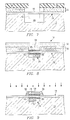
- Figure 9 is a cross-sectional view of the structure of Figure 8 following etching and during a first self-aligned impurity implantation process.
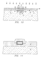
- Figure 10 is a view of the structure of Figure 9 during a second self-aligned impurity implantation process.
- Figure 11 is a cross-sectional view of the structure of Figure 10 taken along lines B-B of Figure 3.
- Figure 1 is a cross-sectional view of a
semiconductor device 10 according to the present invention.Device 10, which is an FET, includes an insulatingsupport 12 and a strip ofsemiconductor material 14. In one aspect of the invention, insulatingsupport 12 is formed from a dielectric such as SiO₂ or glass over a semiconductor substrate, andstrip 14 is formed from polysilicon to form a TFT.Strip 14 includes achannel 16 and source and drainregions gate insulator 22 encircleschannel 16, and agate electrode 24 encirclesgate insulator 22. Becausegate electrode 24 completely encircleschannel 16, the on current and transconductance ofdevice 10 is increased approximately 2-5 times greater than the on current and transconductance of a device having a gate electrode along only a top portion of thechannel 16 surface. Additionally,device 10 may include lightly doped source and drainregions drain 20 to reduce the tendency of electrons fromdrain 20 to become lodged ingate insulator 22. Such lodging, commonly referred to as the "hot electron" problem, may over time shift the threshold voltage ofdevice 10. Furthermore, as discussed below,gate electrode 24 is self-aligned to channel 16. Such self-alignment significantly reduces the size of the device and also reduces parasitic capacitances such as the Miller capacitance, and therefore increases the switching speed ofdevice 10. - Figures 2-10, illustrate a method for forming
device 10. Referring to Figure 2,strip 14 of semiconductor material, having a width W, is formed on an insulatingsupport 12. In one aspect of the invention, thestrip 14 is a layer of amorphous silicon deposited on insulatingsupport 12, which is an SiO₂ layer over a silicon substrate, with a low pressure chemical vapor deposition (LPCVD) process. The thickness of the amorphous silicon film is in the range of approximately 500 - 2500 Å. Typically, the thinner the film, the lower the threshold voltage of the TFT. The deposition temperature is preferably kept between 475 - 650°C so that few nuclei are present for the subsequent grain growth process. The amorphous silicon may be deposited using a source gas of either SiHi₄, which is the conventional gas used, or Si₂H₆. Si₂H₆ allows the LPCVD to be performed at approximately 475°C and still produce a film that is acceptable. For some devices, such as liquid crystal displays (LCDs), the insulatingsupport 12 may be glass or quartz. An LPCVD process at such a low temperature (approximately 475°C) allows insulatingsupport 12 to be glass or quartz. - Alternatively, the
silicon film 14 may be formed as polysilicon. Typical polysilicon formation temperatures range from 650 - 950°C for forming polysilicon on an SiO₂ layer over a silicon substrate. In one embodiment, this polysilicon film may then be made amorphous by ion implantation of silicon. Typically, an implantation level of about 5 x 10¹⁵ atoms/cm at about 75 KEV is sufficient, although the level may vary depending upon the thickness of the deposited film. The growth conditions, and subsequent implant, if necessary, should be such that the deposited film is made as amorphous as possible. Alternatively, thestrip 14 may remain polycrystalline silicon and the inventive device formed from polycrystalline silicon as the channel, source and drainregions - Next, the
amorphous silicon film 14 is exposed to a relatively long, low temperature anneal in N₂ or AR to convert the amorphous silicon to large grained polysilicon. Specifically, this anneal is performed at temperatures approximately in the range of 475 - 600°C and for a time period approximately in the range of 20 - 100 hours. However, the temperature during the annealing process is low enough to prohibit the generation of additional nucleation sites or small crystals, but high enough to allow existing crystallites to grow through solid-state diffusion. Such an annealing process produces a polysilicon film having grain sizes of approximately 5 µm and larger. Alternatively, the amorphous silicon film may be converted to large grain polysilicon by using existing laser recrystallization methods. - The amorphous silicon film is converted into large-grained polysilicon because larger grains produce improved TFTs. For example, the larger grains typically reduce the number of charges that may be stored at carrier traps located mainly at the grain boundaries. Conversely, small grains often generate many such traps, which often force a significant portion of the gate voltage applied to the TFT to be wasted in the work of charging and discharging these trap sites instead of creating an inversion layer, i.e., forming the channel, to turn the TFT on. To further reduce the charge density at the grain boundaries, the polysilicon layer may be passivated with hydrogen (H). Such passivation reduces the threshold voltage and sub threshold leakage currents of the TFT. There are many known ways in which the polysilicon layer may be hydrogen passivated, including a long bake in an appropriate forming gas or H, applying plasma-enhanced chemical vapor deposition (PECVD) silicon nitride layers, immersing the
semiconductor structure 10 in a hydrogen plasma at approximately 300°C, or by high-dose ion implantation with protons. - Alternatively, acceptably large grained polycrystalline silicon may be formed for
strip 14 using any suitable technique, including the direct formation of polysilicon on a glass or SiO₂ layer. - Once the
polysilicon layer 14 has been formed on insulatingsupport 12, one or more polysilicon strips 14 are formed using existing photolithography methods. In one aspect of the invention, width W is 2λ, where 2λ is the minimum feature-size capability for the width of thepolysilicon layer 14 for the process technology being used. - Referring to Figure 3, after the formation of
polysilicon strip 14, aplanar layer 30 is formed over insulatingsupport 12 andstrip 14. In one aspect of the invention,layer 30 includes alayer 32 of silicon dioxide (SiO₂) that is approximately 2,000 Å thick, and alayer 34 of phosphorous glass or boron doped glass that is approximately 5,000 Å thick.Layer 34 is then flowed to give a planar surface 36. In one aspect of the invention,SiO₂ layer 32 is deposited using either a conformal chemical vapor deposition or a low pressure chemical vapor deposition. Next,layer 34 is flowed at an appropriate temperature, typically in the range of 800°-1100°C for some applications, though lower temperatures may be used if desired to give approximately flat upper surface 36. Alternatively,layer 30 having planar surface 36 may be formed from a spin-on glass film using existing techniques. This is useful for LCDs formed on glass or quartz. - Referring to Figure 4, which is a top view of the structure of Figure 3, a
photoresist mask 38 is formed on surface 36 and etched to exposemidsection 16, which has a length L. In one embodiment of the invention, length L is approximately equal to width W. The exposed portions oflayer 30 and insulatingsupport 12 are anisotropically etched to give a structure having the view shown in Figure 5 taken along lines A-A of Figure 4. An anisotropic etch process having a high SiO₂ to Si selectivity is preferred. Such an anisotropic etch may be performed using existing ion-assisted plasma etch processes that use various fluorocarbon plasma chemistries. As shown in Figure 5, the anisotropic etch completely removes the exposed portion oflayer 30 and etches into insulating support 12 a depth of approximately λ, which is about W/2, below the bottom of themidsection 16. Thus, this anisotropic etch forms on either side ofstrip 14, at themidsection 16,open regions 42. - Referring to Figure 6, the exposed portions of insulating
support 12 andlayer 30 are then isotropically etched to give an undercut whose boundary is shown by dottedline 40. The amount of undercut withinregions 42 is such that an intermediate cavity 46 (Figure 7), which is beneathmidsection 16, is formed because the insulatinglayer 12 is etched through under themidsection 16. Such an isotropic etch may be performed using an aqueous solution of HF, such as buffered oxide etch (BOE), to a desired depth. In one embodiment, a depth approximately W/2 beyond the original depth ofopenings 42 after the anisotropic etch is appropriate. However, a smaller undercut is desired in some designs and, for a large gate electrode, a larger undercut is desired, as much as 2λ or greater. - Referring to Figure 7, which is a cross-sectional view taken along lines B-B of Figure 6, one can see that
cavity 46 is formed beneathmidsection 16 ofstrip 14. The dotted line shows the depth ofopenings 42 and the solid line thecavity 46 after the isotropic etch. - Referring to Figure 8, a gate insulator or dielectric 48 is formed such that it completely encircles
midsection 16 ofstrip 14. Because the length ofmidsection 16 is defined by the width ofcavity 46, the gate electrode will be self-aligned withmidsection 16, which will become the channel region of the TFT. Such self-alignment will reduce the Miller parasitic capacitance, which can be increased if the gate electrode overlaps the source or drainregions 18 and 20 (Figure 1). The thickness ofgate insulator 48 may vary within the range of approximately 150 - 500 Å, depending upon the desired threshold voltage.Gate insulator 48 may be formed using a combination of thermal oxidation followed by conformal CVD of tetra-ethyl-ortho-silicate (TEOS)-based silicon dioxide Alternatively,gate insulator 48 may be grown thermally in dry oxygen (O₂). Or,gate insulator 48 may be formed using only CVD as is used to form existing TFTs, or using a chemical-vapor deposited silicon-nitride-gate dielectric process. In one aspect of the invention, beforegate insulator 48 is formed, the exposedmidsection 16 can be thinned by light oxidation and a BOE etching if desired to form a specific-size device. - Next,
midsection 16 is implanted with a suitable dopant to form the channel of the TFT. For example, to form an N-channel transistor,midsection 16 may be implanted with boron in the range of approximately 10¹ atoms/cm. Alternatively, to form a P-channel device,channel region 16 may be left undoped, though typically thechannel 16 is lightly implanted with arsenic (As), to have the desired threshold characteristics selected by the designer using known design tools.Mask layer 38 is removed either before or aftermidsection 16 is implanted to form thechannel 16. - Still referring to Figure 8,
structure 10 is then coated with alayer 50 of polysilicon. As shown,layer 50 completely fills inopenings 42 andcavity 46 to completely encircle bothgate oxide 48 andchannel 16. Depending upon the deposition process used, somevoids 52 may exist in the portion ofpolysilicon layer 50 in thecavity 46 beneathchannel 16. However, it is believed that such voids have no adverse effect on the performance of the resulting TFT, and may be avoided altogether in some polysilicon deposition techniques. - After it has been deposited,
polysilicon layer 50 is doped and etched to the surface ofglass layer 30. In one aspect of the invention,polysilicon layer 50 is first doped with an N⁺ implant or diffusion. The top portion oflayer 50 may be removed with existing processes, such as chemical mechanical polishing (CMP), or ifphotoresist mask 38 has small enough openings, an anisotropic plasma etch may be used to remove thepoly layer 50. The plasma chemistry should have a high selectivity of Si to SiO₂ such as that found in SF₆-based ion-assisted plasma etching. Altematively, the top portion oflayer 50 may be etched first, and the portion oflayer 50 remaining incavity 46 andopenings 42, i.e., the portion oflayer 50 that formsgate electrode 24, may be doped afterwards. Depending upon the doping process used, theupper portion 54 ofgate electrode 24 may be more highly doped than the lower portion. - Referring to Figure 9, at this point in the process,
layer 30 may be removed, and the end portions ofstrip 14 adjacent to channel 16 may be suitably doped to form source and drainregions 18 and 20 (Figure 1) of the TFT. The doping of the source and drainregions gate electrode 24. A later diffusing step will drive the dopant under thechannel 16, intolower portions 54 to ensure that it is doped, if it has not already been doped in a previous step. The source and drainregions gate electrode 24. - The
layer 30 is etched back using an appropriate masking scheme to formspacers 56. In one aspect of the invention, the width S ofspacers 56 is approximately 0.5 µm. As is known in the prior art, where S equals approximately 0.15 µm, the on/off current ratio for the resulting TFT is approximately 10⁴ as compared to 10 for non-LDD devices. Furthermore, the on/off current ratio where S equals approximately 0.45 µm is approximately 10⁷. Following the formation ofspacers 56,strip 14 is implanted with a dopant. For example, in one aspect of the invention,layer 14 is doped with As using an implant level of approximately 10¹⁵ atom/cm to form N+ source and drainregions spacers 56. - Referring to Figure 10,
spacers 56 may then be removed such as with a BOE or plasma etching. Next, a light dose of dopant is implanted to form lightly-dopedregions regions oxide layer 58. Thestructure 10 may then be lightly oxidized to heal any edge voids in thegate dielectric 48. The dopants may then be activated by using rapid thermal annealing (RTA) to reduce lateral diffusion. - In an alternative embodiment of the invention, after the
glass layer 30 is removed, and an implant oxide is formed overstrip 14 andgate electrode 24, a light dopant implant may be performed to formdrain regions spacers 56 are formed and a second implant is performed such thatregions spacer 16 remain lightly doped and the remaining portions of source and drain 18 and 20 become highly doped to give a resulting TFT with lightly doped drain andsource regions - Figure 11 shows a cross-sectional view of the completed TFT as viewed along lines AA of Figure 4. As will be appreciated, the appropriate electrical interconnections to the source and drain
regions polysilicon transistor 10 can become an element of a larger circuit. The contacts can be from a lower layer to adevice 10 or from a higher layer. Most likely, the electrical interconnections will contact source/drain regions gate electrode 24 to another conductor to provide transistor operations, diode connections, load connections, or the like, as required for each circuit design. The standard techniques known in the art today for forming electrical contacts to poly one, poly two, and other layers, may be used. - It will be appreciated that, although a specific embodiment of the invention has been described herein for purposes of illustration, various modifications may be made without departing from the spirit and scope of the invention. Accordingly, the invention is not limited except as by the appended claims.
Claims (15)
- A semiconductor device, comprising:an insulating support;a strip of semiconductor material having two ends contacting said insulating support and a midsection extending between said ends;a layer of dielectric material encircling said midsection; anda layer of conductive material encircling said dielectric layer and having a substantially constant width.
- The device of claim 1 wherein a first of said ends forms a drain region, a second of said ends forms a source region, and said midsection forms a channel region.
- The device of claim 1 or claim 2 wherein said midsection is substantially planar with respect of said ends and said insulating support.
- A semiconductor device, comprising:a body of semiconductor material having a source region, a drain region, and a channel region;a gate insulator encircling said channel region; anda gate electrode encircling said gate insulator and completely self-aligned with said source and drain regions.
- The device of claim 4 wherein said source region and said drain region each comprise a lightly doped region adjacent to said channel region.
- A semiconductor device comprising:first and second doped semiconductor regions spaced from each other;a third doped semiconductor region positioned between said first and second regions, said third region having a lower doping concentration than said first and second regions;an insulator encircling said third region; anda layer of conductive material encircling said insulator and having a substantially constant width.
- The device of claim 6 wherein said first and second regions are of a first type of semiconductor material and wherein said third region is of a second type of semiconductor material.
- The device of claim 6 or claim 7 wherein said first and second regions include lightly doped regions adjacent said third region.
- A method for forming a semiconductor device, comprising:forming a strip of semiconductor material on an insulating support;forming a cavity in said insulating support beneath a midsection of said strip;forming an insulator around said midsection; andforming a self-aligned electrode around said insulator.
- The method of claim 9 wherein said step of forming a cavity comprises:anisotropically etching openings along opposing sides of said midsection; andisotropically etching said openings such that said openings merge to form said cavity.
- The method of claim 9 or claim 10, further comprising doping said midsection to form a channel region and doping ends of said strip adjacent said midsection to form source and drain regions.
- A method for forming a transistor, comprising:forming a strip of semiconductor material on an insulating support;forming a cavity in said insulating support beneath a midsection of said strip such that ends of said film adjacent said midsection are in contact with said insulating support;forming a gate insulator around said channel;forming a channel of the transistor within said midsection;forming a gate electrode around said gate insulator; andforming drain and source regions of the transistor within respective ones of said ends such that said gate electrode is fully self-aligned with said drain and source regions.
- The method of claim 12 wherein said step of forming a strip comprises:forming a layer of polysilicon on said insulating support; andetching said layer to form said strip.
- The method of claim 12 wherein said step of forming a strip comprises:forming a layer of amorphous silicon on said insulating support;etching said layer to form said strip;forming a first dielectric layer over said insulating support and said strip;forming a second dielectric layer over said first dielectric layer; andflowing said first and second dielectric layers to form a planar surface and to convert said amorphous silicon into polysilicon.
- The method of claim 12 wherein said step of forming said cavity comprises:forming on said strip and said insulating support a layer having a substantially planar surface;forming on said layer a mask that exposes said midsection;anisotropically etching said layer and said insulating support to form openings adjacent sides of said midsection; andisotropically etching said insulating support such that said openings merge beneath said midsection to form said cavity.
Applications Claiming Priority (2)
| Application Number | Priority Date | Filing Date | Title |
|---|---|---|---|
| US08/315,955 US5705405A (en) | 1994-09-30 | 1994-09-30 | Method of making the film transistor with all-around gate electrode |
| US315955 | 1999-05-21 |
Publications (3)
| Publication Number | Publication Date |
|---|---|
| EP0704909A2 true EP0704909A2 (en) | 1996-04-03 |
| EP0704909A3 EP0704909A3 (en) | 1997-09-10 |
| EP0704909B1 EP0704909B1 (en) | 2001-07-04 |
Family
ID=23226822
Family Applications (1)
| Application Number | Title | Priority Date | Filing Date |
|---|---|---|---|
| EP95306521A Expired - Lifetime EP0704909B1 (en) | 1994-09-30 | 1995-09-15 | Method for MOS-type semiconductor device |
Country Status (4)
| Country | Link |
|---|---|
| US (2) | US5705405A (en) |
| EP (1) | EP0704909B1 (en) |
| JP (1) | JP3869037B2 (en) |
| DE (1) | DE69521579T2 (en) |
Cited By (2)
| Publication number | Priority date | Publication date | Assignee | Title |
|---|---|---|---|---|
| WO2000074143A1 (en) * | 1999-05-28 | 2000-12-07 | Infineon Technologies Ag | Double gate mosfet transistor and method for the production thereof |
| WO2000079602A1 (en) * | 1999-06-22 | 2000-12-28 | Infineon Technologies Ag | Multi-channel mosfet and method for producing the same |
Families Citing this family (46)
| Publication number | Priority date | Publication date | Assignee | Title |
|---|---|---|---|---|
| US6060375A (en) * | 1996-07-31 | 2000-05-09 | Lsi Logic Corporation | Process for forming re-entrant geometry for gate electrode of integrated circuit structure |
| US6962883B2 (en) * | 1996-08-01 | 2005-11-08 | Texas Instruments Incorporated | Integrated circuit insulator and method |
| KR100331845B1 (en) * | 1998-01-10 | 2002-05-10 | 박종섭 | Method for fabricating of thin film transistor |
| US6117712A (en) * | 1998-03-13 | 2000-09-12 | Texas Instruments - Acer Incorporated | Method of forming ultra-short channel and elevated S/D MOSFETS with a metal gate on SOI substrate |
| US6207530B1 (en) | 1998-06-19 | 2001-03-27 | International Business Machines Corporation | Dual gate FET and process |
| DE69832162D1 (en) * | 1998-07-22 | 2005-12-08 | St Microelectronics Srl | A fabrication process for an electronic device including MOS transistors with salicided junctions and non-salicided resistors |
| US6162688A (en) * | 1999-01-14 | 2000-12-19 | Advanced Micro Devices, Inc. | Method of fabricating a transistor with a dielectric underlayer and device incorporating same |
| US6103563A (en) * | 1999-03-17 | 2000-08-15 | Advanced Micro Devices, Inc. | Nitride disposable spacer to reduce mask count in CMOS transistor formation |
| FR2799305B1 (en) * | 1999-10-05 | 2004-06-18 | St Microelectronics Sa | METHOD FOR MANUFACTURING A SEMICONDUCTOR DEVICE WITH ENVELOPING GRID AND DEVICE OBTAINED |
| US6376286B1 (en) * | 1999-10-20 | 2002-04-23 | Advanced Micro Devices, Inc. | Field effect transistor with non-floating body and method for forming same on a bulk silicon wafer |
| US6465852B1 (en) | 1999-10-20 | 2002-10-15 | Advanced Micro Devices, Inc. | Silicon wafer including both bulk and SOI regions and method for forming same on a bulk silicon wafer |
| US6245636B1 (en) | 1999-10-20 | 2001-06-12 | Advanced Micro Devices, Inc. | Method of formation of pseudo-SOI structures with direct contact of transistor body to the substrate |
| US6391658B1 (en) * | 1999-10-26 | 2002-05-21 | International Business Machines Corporation | Formation of arrays of microelectronic elements |
| ATE378692T1 (en) * | 2000-02-29 | 2007-11-15 | Nxp Bv | DOUBLE GATE SEMICONDUCTOR COMPONENT AND PRODUCTION METHOD THEREOF |
| DE10012112C2 (en) * | 2000-03-13 | 2002-01-10 | Infineon Technologies Ag | Bridge field effect transistor and method for producing a bridge field effect transistor |
| US6982460B1 (en) * | 2000-07-07 | 2006-01-03 | International Business Machines Corporation | Self-aligned gate MOSFET with separate gates |
| US6563131B1 (en) | 2000-06-02 | 2003-05-13 | International Business Machines Corporation | Method and structure of a dual/wrap-around gate field effect transistor |
| JP2002034179A (en) * | 2000-07-14 | 2002-01-31 | Toshiba Corp | Power controller |
| DE10045045C2 (en) * | 2000-09-12 | 2002-09-19 | Infineon Technologies Ag | Manufacturing process of field effect transistors in semiconductor integrated circuits |
| US6630388B2 (en) * | 2001-03-13 | 2003-10-07 | National Institute Of Advanced Industrial Science And Technology | Double-gate field-effect transistor, integrated circuit using the transistor and method of manufacturing the same |
| US7189997B2 (en) | 2001-03-27 | 2007-03-13 | Semiconductor Energy Laboratory Co., Ltd. | Semiconductor device and method for manufacturing the same |
| US6982194B2 (en) * | 2001-03-27 | 2006-01-03 | Semiconductor Energy Laboratory Co., Ltd. | Semiconductor device and method for manufacturing the same |
| US6740938B2 (en) * | 2001-04-16 | 2004-05-25 | Semiconductor Energy Laboratory Co., Ltd. | Transistor provided with first and second gate electrodes with channel region therebetween |
| FR2838238B1 (en) * | 2002-04-08 | 2005-04-15 | St Microelectronics Sa | SEMICONDUCTOR DEVICE WITH ENVELOPING GRID ENCAPSULATED IN AN INSULATING MEDIUM |
| US6995430B2 (en) * | 2002-06-07 | 2006-02-07 | Amberwave Systems Corporation | Strained-semiconductor-on-insulator device structures |
| US7074623B2 (en) * | 2002-06-07 | 2006-07-11 | Amberwave Systems Corporation | Methods of forming strained-semiconductor-on-insulator finFET device structures |
| US20030227057A1 (en) * | 2002-06-07 | 2003-12-11 | Lochtefeld Anthony J. | Strained-semiconductor-on-insulator device structures |
| US6833588B2 (en) * | 2002-10-22 | 2004-12-21 | Advanced Micro Devices, Inc. | Semiconductor device having a U-shaped gate structure |
| US6686231B1 (en) * | 2002-12-06 | 2004-02-03 | Advanced Micro Devices, Inc. | Damascene gate process with sacrificial oxide in semiconductor devices |
| US6864164B1 (en) | 2002-12-17 | 2005-03-08 | Advanced Micro Devices, Inc. | Finfet gate formation using reverse trim of dummy gate |
| US6855606B2 (en) * | 2003-02-20 | 2005-02-15 | Taiwan Semiconductor Manufacturing Company, Ltd. | Semiconductor nano-rod devices |
| US7074656B2 (en) * | 2003-04-29 | 2006-07-11 | Taiwan Semiconductor Manufacturing Company, Ltd. | Doping of semiconductor fin devices |
| KR100471173B1 (en) | 2003-05-15 | 2005-03-10 | 삼성전자주식회사 | Transistor having multi channel and method of fabricating the same |
| US6855582B1 (en) | 2003-06-12 | 2005-02-15 | Advanced Micro Devices, Inc. | FinFET gate formation using reverse trim and oxide polish |
| US7271444B2 (en) * | 2003-12-11 | 2007-09-18 | International Business Machines Corporation | Wrap-around gate field effect transistor |
| US7041542B2 (en) * | 2004-01-12 | 2006-05-09 | Advanced Micro Devices, Inc. | Damascene tri-gate FinFET |
| KR100526887B1 (en) * | 2004-02-10 | 2005-11-09 | 삼성전자주식회사 | Field Effect Transistor and method for manufacturing at the same |
| US7084018B1 (en) | 2004-05-05 | 2006-08-01 | Advanced Micro Devices, Inc. | Sacrificial oxide for minimizing box undercut in damascene FinFET |
| US7452778B2 (en) * | 2004-06-10 | 2008-11-18 | Taiwan Semiconductor Manufacturing Company, Ltd. | Semiconductor nano-wire devices and methods of fabrication |
| WO2006070309A1 (en) * | 2004-12-28 | 2006-07-06 | Koninklijke Philips Electronics N.V. | Semiconductor device having strip- shaped channel and method for manufacturing such a device |
| JP4405412B2 (en) * | 2005-03-02 | 2010-01-27 | 株式会社東芝 | Semiconductor integrated circuit |
| US7709313B2 (en) * | 2005-07-19 | 2010-05-04 | International Business Machines Corporation | High performance capacitors in planar back gates CMOS |
| EP1938381A2 (en) * | 2005-09-23 | 2008-07-02 | Nanosys, Inc. | Methods for nanostructure doping |
| US9054194B2 (en) * | 2009-04-29 | 2015-06-09 | Taiwan Semiconductor Manufactruing Company, Ltd. | Non-planar transistors and methods of fabrication thereof |
| WO2014168876A2 (en) | 2013-04-08 | 2014-10-16 | Perkinelmer Health Sciences, Inc. | Capacitively coupled devices and oscillators |
| KR102191215B1 (en) | 2013-12-20 | 2020-12-16 | 삼성전자주식회사 | Static random access memory (sram) cell and method of manufacturing the same |
Citations (4)
| Publication number | Priority date | Publication date | Assignee | Title |
|---|---|---|---|---|
| EP0418983A1 (en) * | 1989-09-21 | 1991-03-27 | Interuniversitair Microelektronica Centrum Vzw | Method of manufacturing a field effect transistor and a semiconductor element |
| EP0487220A2 (en) * | 1990-11-19 | 1992-05-27 | Mitsubishi Denki Kabushiki Kaisha | SOI-Field effect transistor and method of manufacturing the same |
| US5120666A (en) * | 1989-05-16 | 1992-06-09 | Fujitsu Limited | Manufacturing method for semiconductor device |
| EP0612103A2 (en) * | 1993-02-17 | 1994-08-24 | Samsung Electronics Co., Ltd. | Method of manufacturing a silicon-on-insulator semiconductor device |
Family Cites Families (16)
| Publication number | Priority date | Publication date | Assignee | Title |
|---|---|---|---|---|
| JPS62274662A (en) * | 1986-05-22 | 1987-11-28 | Seiko Epson Corp | Mis type semiconductor device |
| JPS63308386A (en) * | 1987-01-30 | 1988-12-15 | Sony Corp | Semiconductor device and manufacture thereof |
| JPH0227772A (en) * | 1988-07-15 | 1990-01-30 | Sony Corp | Field effect type thin film transistor |
| US5135888A (en) * | 1989-01-18 | 1992-08-04 | Sgs-Thomson Microelectronics, Inc. | Field effect device with polycrystalline silicon channel |
| JP2804539B2 (en) * | 1989-09-28 | 1998-09-30 | 沖電気工業株式会社 | Semiconductor device and manufacturing method thereof |
| JPH0479424U (en) * | 1990-11-23 | 1992-07-10 | ||
| JP2794678B2 (en) * | 1991-08-26 | 1998-09-10 | 株式会社 半導体エネルギー研究所 | Insulated gate semiconductor device and method of manufacturing the same |
| JPH04318972A (en) * | 1991-04-17 | 1992-11-10 | Kawasaki Steel Corp | Semiconductor element |
| US5204279A (en) * | 1991-06-03 | 1993-04-20 | Sgs-Thomson Microelectronics, Inc. | Method of making SRAM cell and structure with polycrystalline p-channel load devices |
| US5187114A (en) * | 1991-06-03 | 1993-02-16 | Sgs-Thomson Microelectronics, Inc. | Method of making SRAM cell and structure with polycrystalline P-channel load devices |
| JPH0529573A (en) * | 1991-07-24 | 1993-02-05 | Mitsubishi Electric Corp | Semiconductor storage device and manufacture thereof |
| JP2650543B2 (en) * | 1991-11-25 | 1997-09-03 | カシオ計算機株式会社 | Matrix circuit drive |
| KR950002202B1 (en) * | 1992-07-01 | 1995-03-14 | 현대전자산업주식회사 | Making method of stack tft |
| US5302842A (en) * | 1992-07-20 | 1994-04-12 | Bell Communications Research, Inc. | Field-effect transistor formed over gate electrode |
| US5324673A (en) * | 1992-11-19 | 1994-06-28 | Motorola, Inc. | Method of formation of vertical transistor |
| US5482871A (en) * | 1994-04-15 | 1996-01-09 | Texas Instruments Incorporated | Method for forming a mesa-isolated SOI transistor having a split-process polysilicon gate |
-
1994
- 1994-09-30 US US08/315,955 patent/US5705405A/en not_active Expired - Lifetime
-
1995
- 1995-05-30 US US08/452,893 patent/US5801397A/en not_active Expired - Lifetime
- 1995-09-15 DE DE69521579T patent/DE69521579T2/en not_active Expired - Fee Related
- 1995-09-15 EP EP95306521A patent/EP0704909B1/en not_active Expired - Lifetime
- 1995-09-28 JP JP25147495A patent/JP3869037B2/en not_active Expired - Lifetime
Patent Citations (4)
| Publication number | Priority date | Publication date | Assignee | Title |
|---|---|---|---|---|
| US5120666A (en) * | 1989-05-16 | 1992-06-09 | Fujitsu Limited | Manufacturing method for semiconductor device |
| EP0418983A1 (en) * | 1989-09-21 | 1991-03-27 | Interuniversitair Microelektronica Centrum Vzw | Method of manufacturing a field effect transistor and a semiconductor element |
| EP0487220A2 (en) * | 1990-11-19 | 1992-05-27 | Mitsubishi Denki Kabushiki Kaisha | SOI-Field effect transistor and method of manufacturing the same |
| EP0612103A2 (en) * | 1993-02-17 | 1994-08-24 | Samsung Electronics Co., Ltd. | Method of manufacturing a silicon-on-insulator semiconductor device |
Non-Patent Citations (1)
| Title |
|---|
| INTERNATIONAL ELECTRON DEVICES MEETING, SAN FRANCISCO, DEC. 9 - 12, 1990, no. -, 9 December 1990, INSTITUTE OF ELECTRICAL AND ELECTRONICS ENGINEERS, pages 595-598, XP000279606 COLINGE J P ET AL: "SILICON-ON-INSULATOR "GATE-ALL-AROUND DEVICE"" * |
Cited By (3)
| Publication number | Priority date | Publication date | Assignee | Title |
|---|---|---|---|---|
| WO2000074143A1 (en) * | 1999-05-28 | 2000-12-07 | Infineon Technologies Ag | Double gate mosfet transistor and method for the production thereof |
| US6864129B2 (en) | 1999-05-28 | 2005-03-08 | Infineon Technologies Ag | Double gate MOSFET transistor and method for the production thereof |
| WO2000079602A1 (en) * | 1999-06-22 | 2000-12-28 | Infineon Technologies Ag | Multi-channel mosfet and method for producing the same |
Also Published As
| Publication number | Publication date |
|---|---|
| JP3869037B2 (en) | 2007-01-17 |
| US5705405A (en) | 1998-01-06 |
| EP0704909A3 (en) | 1997-09-10 |
| DE69521579D1 (en) | 2001-08-09 |
| JPH08181328A (en) | 1996-07-12 |
| EP0704909B1 (en) | 2001-07-04 |
| US5801397A (en) | 1998-09-01 |
| DE69521579T2 (en) | 2002-05-29 |
Similar Documents
| Publication | Publication Date | Title |
|---|---|---|
| EP0704909B1 (en) | Method for MOS-type semiconductor device | |
| US5998847A (en) | Low voltage active body semiconductor device | |
| US7259049B2 (en) | Self-aligned isolation double-gate FET | |
| US5930642A (en) | Transistor with buried insulative layer beneath the channel region | |
| US5166084A (en) | Process for fabricating a silicon on insulator field effect transistor | |
| US6545327B2 (en) | Semiconductor device having different gate insulating films with different amount of carbon | |
| US6124614A (en) | Si/SiGe MOSFET and method for fabricating the same | |
| KR100265080B1 (en) | A vertical double-gate field effect transistor | |
| US7879675B2 (en) | Field effect transistor with metal source/drain regions | |
| US5663586A (en) | Fet device with double spacer | |
| US7259048B2 (en) | Vertical replacement-gate silicon-on-insulator transistor | |
| US7687365B2 (en) | CMOS structure for body ties in ultra-thin SOI (UTSOI) substrates | |
| US5656518A (en) | Method for fabrication of a non-symmetrical transistor | |
| US5904508A (en) | Semiconductor device and a method of manufacturing the same | |
| JPS63255967A (en) | Manufacture of field effect transistor | |
| US20040121549A1 (en) | Self-aligned planar double-gate process by amorphization | |
| US5235189A (en) | Thin film transistor having a self-aligned gate underlying a channel region | |
| US6724049B2 (en) | SOI semiconductor device with insulating film having different properties relative to the buried insulating film | |
| US7648880B2 (en) | Nitride-encapsulated FET (NNCFET) | |
| US6184070B1 (en) | Thin film transistor and method of manufacturing the same | |
| US5158898A (en) | Self-aligned under-gated thin film transistor and method of formation | |
| US20050158923A1 (en) | Ultra-thin body transistor with recessed silicide contacts | |
| JPS63281465A (en) | Manufacture of field effect transistor and its intermediate product | |
| EP0704910B1 (en) | A thin-film transistor and method for forming the same | |
| JPS63255966A (en) | Field effect transistor |
Legal Events
| Date | Code | Title | Description |
|---|---|---|---|
| PUAI | Public reference made under article 153(3) epc to a published international application that has entered the european phase |
Free format text: ORIGINAL CODE: 0009012 |
|
| AK | Designated contracting states |
Kind code of ref document: A2 Designated state(s): DE FR GB IT |
|
| PUAL | Search report despatched |
Free format text: ORIGINAL CODE: 0009013 |
|
| AK | Designated contracting states |
Kind code of ref document: A3 Designated state(s): DE FR GB IT |
|
| 17P | Request for examination filed |
Effective date: 19980216 |
|
| 17Q | First examination report despatched |
Effective date: 19980515 |
|
| RAP3 | Party data changed (applicant data changed or rights of an application transferred) |
Owner name: STMICROELECTRONICS, INC. |
|
| RTI1 | Title (correction) |
Free format text: MEHTOD FOR MOS-TYPE SEMICONDUCTOR DEVICE |
|
| RTI1 | Title (correction) |
Free format text: METHOD FOR MOS-TYPE SEMICONDUCTOR DEVICE |
|
| GRAG | Despatch of communication of intention to grant |
Free format text: ORIGINAL CODE: EPIDOS AGRA |
|
| GRAG | Despatch of communication of intention to grant |
Free format text: ORIGINAL CODE: EPIDOS AGRA |
|
| GRAH | Despatch of communication of intention to grant a patent |
Free format text: ORIGINAL CODE: EPIDOS IGRA |
|
| GRAH | Despatch of communication of intention to grant a patent |
Free format text: ORIGINAL CODE: EPIDOS IGRA |
|
| GRAA | (expected) grant |
Free format text: ORIGINAL CODE: 0009210 |
|
| AK | Designated contracting states |
Kind code of ref document: B1 Designated state(s): DE FR GB IT |
|
| PG25 | Lapsed in a contracting state [announced via postgrant information from national office to epo] |
Ref country code: IT Free format text: LAPSE BECAUSE OF FAILURE TO SUBMIT A TRANSLATION OF THE DESCRIPTION OR TO PAY THE FEE WITHIN THE PRESCRIBED TIME-LIMIT;WARNING: LAPSES OF ITALIAN PATENTS WITH EFFECTIVE DATE BEFORE 2007 MAY HAVE OCCURRED AT ANY TIME BEFORE 2007. THE CORRECT EFFECTIVE DATE MAY BE DIFFERENT FROM THE ONE RECORDED. Effective date: 20010704 |
|
| REF | Corresponds to: |
Ref document number: 69521579 Country of ref document: DE Date of ref document: 20010809 |
|
| ET | Fr: translation filed | ||
| REG | Reference to a national code |
Ref country code: GB Ref legal event code: IF02 |
|
| PLBE | No opposition filed within time limit |
Free format text: ORIGINAL CODE: 0009261 |
|
| STAA | Information on the status of an ep patent application or granted ep patent |
Free format text: STATUS: NO OPPOSITION FILED WITHIN TIME LIMIT |
|
| 26N | No opposition filed | ||
| PGFP | Annual fee paid to national office [announced via postgrant information from national office to epo] |
Ref country code: FR Payment date: 20050823 Year of fee payment: 11 |
|
| PGFP | Annual fee paid to national office [announced via postgrant information from national office to epo] |
Ref country code: DE Payment date: 20050909 Year of fee payment: 11 |
|
| PGFP | Annual fee paid to national office [announced via postgrant information from national office to epo] |
Ref country code: GB Payment date: 20050914 Year of fee payment: 11 |
|
| PG25 | Lapsed in a contracting state [announced via postgrant information from national office to epo] |
Ref country code: DE Free format text: LAPSE BECAUSE OF NON-PAYMENT OF DUE FEES Effective date: 20070403 |
|
| GBPC | Gb: european patent ceased through non-payment of renewal fee |
Effective date: 20060915 |
|
| REG | Reference to a national code |
Ref country code: FR Ref legal event code: ST Effective date: 20070531 |
|
| PG25 | Lapsed in a contracting state [announced via postgrant information from national office to epo] |
Ref country code: GB Free format text: LAPSE BECAUSE OF NON-PAYMENT OF DUE FEES Effective date: 20060915 |
|
| PG25 | Lapsed in a contracting state [announced via postgrant information from national office to epo] |
Ref country code: FR Free format text: LAPSE BECAUSE OF NON-PAYMENT OF DUE FEES Effective date: 20061002 |