EP0705020A2 - Circuit arrangement for feeding at least a load - Google Patents
Circuit arrangement for feeding at least a load Download PDFInfo
- Publication number
- EP0705020A2 EP0705020A2 EP95202474A EP95202474A EP0705020A2 EP 0705020 A2 EP0705020 A2 EP 0705020A2 EP 95202474 A EP95202474 A EP 95202474A EP 95202474 A EP95202474 A EP 95202474A EP 0705020 A2 EP0705020 A2 EP 0705020A2
- Authority
- EP
- European Patent Office
- Prior art keywords
- supply voltage
- circuit arrangement
- signal
- reference voltage
- identification
- Prior art date
- Legal status (The legal status is an assumption and is not a legal conclusion. Google has not performed a legal analysis and makes no representation as to the accuracy of the status listed.)
- Withdrawn
Links
Images

Classifications
-
- H—ELECTRICITY
- H04—ELECTRIC COMMUNICATION TECHNIQUE
- H04L—TRANSMISSION OF DIGITAL INFORMATION, e.g. TELEGRAPHIC COMMUNICATION
- H04L25/00—Baseband systems
- H04L25/02—Details ; arrangements for supplying electrical power along data transmission lines
- H04L25/0264—Arrangements for coupling to transmission lines
- H04L25/0266—Arrangements for providing Galvanic isolation, e.g. by means of magnetic or capacitive coupling
-
- G—PHYSICS
- G05—CONTROLLING; REGULATING
- G05F—SYSTEMS FOR REGULATING ELECTRIC OR MAGNETIC VARIABLES
- G05F5/00—Systems for regulating electric variables by detecting deviations in the electric input to the system and thereby controlling a device within the system to obtain a regulated output
-
- H—ELECTRICITY
- H02—GENERATION; CONVERSION OR DISTRIBUTION OF ELECTRIC POWER
- H02J—CIRCUIT ARRANGEMENTS OR SYSTEMS FOR SUPPLYING OR DISTRIBUTING ELECTRIC POWER; SYSTEMS FOR STORING ELECTRIC ENERGY
- H02J13/00—Circuit arrangements for providing remote indication of network conditions, e.g. an instantaneous record of the open or closed condition of each circuitbreaker in the network; Circuit arrangements for providing remote control of switching means in a power distribution network, e.g. switching in and out of current consumers by using a pulse code signal carried by the network
- H02J13/00006—Circuit arrangements for providing remote indication of network conditions, e.g. an instantaneous record of the open or closed condition of each circuitbreaker in the network; Circuit arrangements for providing remote control of switching means in a power distribution network, e.g. switching in and out of current consumers by using a pulse code signal carried by the network characterised by information or instructions transport means between the monitoring, controlling or managing units and monitored, controlled or operated power network element or electrical equipment
- H02J13/00016—Circuit arrangements for providing remote indication of network conditions, e.g. an instantaneous record of the open or closed condition of each circuitbreaker in the network; Circuit arrangements for providing remote control of switching means in a power distribution network, e.g. switching in and out of current consumers by using a pulse code signal carried by the network characterised by information or instructions transport means between the monitoring, controlling or managing units and monitored, controlled or operated power network element or electrical equipment using a wired telecommunication network or a data transmission bus
-
- H—ELECTRICITY
- H04—ELECTRIC COMMUNICATION TECHNIQUE
- H04B—TRANSMISSION
- H04B3/00—Line transmission systems
- H04B3/02—Details
- H04B3/44—Arrangements for feeding power to a repeater along the transmission line
-
- H—ELECTRICITY
- H04—ELECTRIC COMMUNICATION TECHNIQUE
- H04L—TRANSMISSION OF DIGITAL INFORMATION, e.g. TELEGRAPHIC COMMUNICATION
- H04L25/00—Baseband systems
- H04L25/02—Details ; arrangements for supplying electrical power along data transmission lines
- H04L25/0264—Arrangements for coupling to transmission lines
- H04L25/0272—Arrangements for coupling to multiple lines, e.g. for differential transmission
-
- H—ELECTRICITY
- H04—ELECTRIC COMMUNICATION TECHNIQUE
- H04L—TRANSMISSION OF DIGITAL INFORMATION, e.g. TELEGRAPHIC COMMUNICATION
- H04L25/00—Baseband systems
- H04L25/02—Details ; arrangements for supplying electrical power along data transmission lines
- H04L25/0264—Arrangements for coupling to transmission lines
- H04L25/028—Arrangements specific to the transmitter end
-
- H—ELECTRICITY
- H04—ELECTRIC COMMUNICATION TECHNIQUE
- H04L—TRANSMISSION OF DIGITAL INFORMATION, e.g. TELEGRAPHIC COMMUNICATION
- H04L25/00—Baseband systems
- H04L25/02—Details ; arrangements for supplying electrical power along data transmission lines
- H04L25/0264—Arrangements for coupling to transmission lines
- H04L25/0292—Arrangements specific to the receiver end
Definitions
- the invention relates to a circuit arrangement for supplying at least one load from a supply voltage source.
- telecommunication devices particularly if they are arranged outside switching centers or the like, are remotely supplied with electrical energy.
- the signal transmission lines that are already present i.e. Telecommunication lines, but also additional lines can be used.
- a plurality of telecommunications or signal transmission devices can be connected as loads via corresponding lines to a supply voltage source, which is set up, for example, in a telecommunications office. Since there is no longer a direct spatial connection in such systems, special attention must be paid to the fact that the supply voltage source and the loads to be fed are adapted to one another with regard to the services to be provided or to be taken up, in order to avoid damage or malfunctions. In particular, an overload of the supply voltage source, but also an insufficient supply of the loads, can usually still be determined and remedied from the location of the supply voltage source.
- the object of the invention is to design a circuit arrangement for feeding at least one load from a supply voltage source in such a way that damage to the loads caused by excessively high supply voltages, as described by way of example in the foregoing, can be ruled out.
- this object is achieved by a circuit arrangement for supplying at least one load from a supply voltage source, which is set up for supplying a supply voltage, which optionally has a supply voltage value that is lower than a reference voltage and at least one further supply voltage value that is higher than the reference voltage is adjustable, whereby the identification of the load (s) when receiving a supply voltage that is lower than the reference voltage, a characteristic signal (or identification signals) of a predetermined type, through which the supply voltage source a specifiable of the supply voltage values that are higher than the reference voltage can be switched.
- the invention effectively prevents excessive supply voltages from reaching loads that have a lower dielectric strength.
- the supply voltage source is only set to a supply voltage value that is higher than the reference voltage if it has been ensured that the terminals, ie signal processing devices, that are suitable with regard to their supply voltage are connected.
- the operation of such circuit arrangements in particular also a start-up after structural changes, such as those in a telecommunications network are very common, significantly simplified and at the same time significantly improve the security against damage. Furthermore, it is avoided that dangerous voltages can reach the subscriber directly when connected.
- switching to a supply voltage value which is higher than the reference voltage is therefore preferably avoided if no identification signal of the specified type is received by the supply voltage source.
- the supply voltage initially given for example when the supply voltage source is not put into operation, the supply voltage value of which is less than the reference voltage and which can be supplied to all signal transmission devices that can be connected as loads without their damage, is then not increased further, but remains below the reference voltage. If necessary, an error signal can also be emitted by the supply voltage source.
- the loads in particular such signal transmission devices, are equipped with devices for emitting the identification signals, which, in contrast to the other parts of the loads or signal transmission devices, may already be ready for operation with a supply voltage which is lower than the reference voltage, and which is preferably for Saving electrical energy or for protection against damage from overvoltages can be separated from the supply voltage source if the supply voltage assumes a value which is higher than the reference voltage.
- the identification signals can only contain information as to whether the supply voltage value may be increased by the supply voltage source.
- the supply voltage source can, for example, be specifically set to an allowable supply voltage value.
- the identification signals comprise vibrations with a frequency which can be predetermined differently for each of the supply voltage values above the reference voltage.
- the control of the supply voltage source by the identification signals then takes place essentially by a simple frequency selection of the received identification signals.
- the identification signals comprise digital pulse signals which are coded differently for each of the supply voltage values above the reference voltage.
- a digital control of the supply voltage source can thus preferably be carried out.
- Such identification signals are particularly recommended if they are to be used to transmit a larger amount of information, for example also about details of the load being sent and, if appropriate, its place of use.
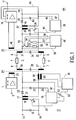
- reference numeral 1 designates a first signal processing device which is used, for example, for signal transmission in a telecommunications system between a connection 2 and a telecommunications line 3.
- the telecommunication line 3 is shown symbolically in FIG. 1 with two ohmic resistors 4, 5, which serve as equivalent circuit diagrams for the actual line impedances of the telecommunication line 3 and are arranged between line end connections 6, 7 and 8, 9, respectively.
- the line end connections 6, 7 form the end of the telecommunication line 3 facing the first signal processing device 1.
- the first signal processing device 1 is arranged, for example, in a telecommunication exchange from which at least one further signal processing device 10 is to be supplied with electrical energy.
- This further signal processing device 10 for example also a telecommunications device, is connected to a second line end formed by the line end connections 8, 9 and has a connection 11.
- telecommunications signals should be able to be transmitted from the connection 2 to the connection 11 and vice versa, the electrical circuit supplying the entire circuit arrangement exclusively from the location of the first signal processing device 1.
- a supply voltage source 12 for the remote supply of the further signal processing device 10 which supplies electrical energy, for example, from an energy supply network can be supplied via two network connections 13, 14.
- the supply voltage source 12 in the example according to FIG. 1 is set up as a switching power supply for generating a supply voltage from a (preferably rectified) mains voltage supplied via the mains connections 13, 14.
- energy from, for example, a central battery or the like can also be supplied via the mains connections 13, 14.
- the switched-mode power supply of the supply voltage source 12 comprises a first smoothing capacitor 15, which is arranged between the mains connections 13, 14, and a series circuit, arranged in parallel, of a primary winding 16 of a first switched-mode power supply transformer 17 with a first chopper switch 18.
- the first chopper switch 18 is shown in FIG. 1 Shown for the sake of simplicity as a mechanical switch, but in practice is preferably designed as an electronic switch. It is switched alternately into a conductive and a blocked state by a control circuit 19, for which purpose a control line 20 is used.
- An AC voltage is tapped from a secondary winding 21 of the first switched-mode power supply transformer 17 and fed to a series circuit comprising a first diode 22 with a second smoothing capacitor 23.
- the supply voltage is then tapped from the connections of the second smoothing capacitor 23 and fed to the line end connections 6 and 7 at the first line end connected to the first signal processing device 1.
- a first line transformer 24 is used to transmit the telecommunications signals between the first signal processing device 1 and the line end connections 6, 7 on the one hand and the electrical energy from the connections of the second smoothing capacitor 23 to the line end connections 6, 7 provided which comprises a primary winding 25 and a secondary winding divided into two parts 26, 27.
- first and the second part 26, 27 of the secondary winding of the first line transformer 24 are connected to the line end connection 6 or 7, whereas the other connections of the part 26, 27 of the secondary winding of the first line transformer 24 each have one of the connections of the second Smoothing capacitor 23 and also connected to each other via a first coupling capacitor 28.
- the first coupling capacitor 28 forms an AC short circuit for the signals to be transmitted from the telecommunication line 3 to the first signal processing device 1 and vice versa.
- the connections of the second smoothing capacitor 23 are also connected to two inputs 29, 30 of the control circuit 19.
- the power supply of the control circuit 19 is carried out via these inputs 29, 30; on the other hand, the voltage supplied via the inputs 29, 30 is used as a control variable for the formation of a control signal to the first chopper switch 18 via the control line 20.
- the control circuit 19 is preferably designed with a pulse width modulator which, via the control line 20, outputs a pulse width modulated pulse signal as a control signal to the first chopper switch 18, which controls it in such a way that the supply voltage at the second smoothing capacitor 23 is at least virtually constant regardless of the load.
- the signal processing device 10 on the second line end formed by the line end connections 8, 9 is likewise supplied with energy by a switching power supply which is fed remotely from the supply voltage source 12 via the telecommunication line 3.
- a switching power supply which is fed remotely from the supply voltage source 12 via the telecommunication line 3.
- the Line end connections 8, 9 at the second line end are bridged by a series connection of two parts 31, 32 of a secondary winding of a second line transformer 33 with a second coupling capacitor 34.
- the voltage losses in the telecommunication line 3 and the secondary windings 26, 27 or 31, 32 of the line transformers 24 or 33 weakened supply voltage tapped from the supply voltage source and fed to the switching power supply for remote supply of the signal processing device 10.
- This comprises a third smoothing capacitor 35 connected in parallel to the second coupling capacitor 34, to which, in turn, a series circuit comprising a primary winding 36 of a second switching power supply transformer 37 with a second chopper switch 38 is arranged in parallel.
- the second chopper switch 38 is switched alternately into the conductive and the blocked state by a second control circuit 39 via a second control line 40.
- a series circuit comprising a second diode 42 with a fourth smoothing capacitor 43 is connected to the connections of a secondary winding 41 of the second switching power supply transformer 37.
- the connections of the fourth smoothing capacitor 43 are tapped off from the supply voltage for the signal processing device 10 via power supply connections 44, 45.
- the fourth smoothing capacitor 43 is also connected with its connections to inputs 46 and 47 of the second control circuit 39, via which the voltage at the fourth smoothing capacitor 43 can be supplied as a supply voltage and at the same time as a measured variable.
- the function of the switching power supply 35 to 43 corresponds to that of the switching power supply 15 to 23 contained in the supply voltage source 12.
- the second line transformer 33 has a primary winding 48 which is magnetically coupled to the secondary winding 31, 32 in the same way as is the case with the first line transformer 24 between its primary winding 25 and its secondary winding 26, 27.
- the connections of the primary winding 48 of the second line transformer 33 are connected to the further signal processing device 10 in accordance with the connection of the connections of the primary winding 25 of the first line transformer 24 to the first signal processing device 1. Coupling and coupling of the telecommunication signals from the signal processing devices 1 and 10 to the telecommunication line 3 In this exemplary embodiment, this is preferably done symmetrically in order to create the same conditions in both transmission directions.
- the circuit arrangement at the second line end 8, 9, that is to say in connection with the remotely fed switching power supply 35 to 43, has a device for generating a characteristic signal which consists of an oscillation of a predeterminable frequency and which is emitted when it is transmitted via the second Line end 8, 9 supplied supply voltage at the second coupling capacitor 34 has a value which is lower than a predetermined reference voltage.
- Said device comprises a comparison stage 49, which is connected with two inputs 50, 51 in parallel to the second coupling capacitor 34 and the third smoothing capacitor 35, respectively. The supply voltage is fed to the comparison stage 49 via the inputs 50, 51.
- the comparison stage 49 is designed such that it is already at the supply voltage value, which is lower than the reference voltage and to which the supply voltage source 12 can be set, is ready for operation, regardless of whether the remote-fed switching power supply 35 to 43 or the signal processing device 10 supplied with energy can already operate at this supply voltage value.
- the supply voltage supplied via the inputs 50, 51 to the comparison stage 49 supplies the latter with electrical energy on the one hand and is used on the other hand for comparison with the predetermined reference voltage, which is preferably generated within the comparison stage 49.
- the described comparison can also be carried out, for example, between a certain fraction of this reference voltage and the same fraction of the supplied supply voltage, or threshold value circuits can be used which are dimensioned for the reference voltage.
- a series circuit comprising a first switch 52 with a first ohmic resistor 53 is arranged, which in turn is bridged by a series circuit comprising a second switch 54 with a second ohmic resistor 55.
- the comparison stage 49 has a first and a second control output 56 and 57, which are connected to the first and second switches 52 and 54, respectively. Via the first control output 56, the first switch 52 is brought into its conductive state by the comparison stage 49 if the supply voltage at the inputs 50, 51 of the comparison stage 49 is less than the reference voltage, and the first switch 52 is brought into its blocked state, if the supply voltage at the inputs 50, 51 the reference voltage exceeds.
- the switching stage 49 emits a switching signal with the frequency of the identification signal, by means of which the second switch 54 is alternately switched on or off.
- the first switch 52 is conductive, an oscillation is thus transmitted from the comparison stage 49 via the second switch 54 to the second line end 8, 9 and transported via the telecommunication line 3 to its first line end 6, 7.
- this identification signal is interrupted by the first switch 52.
- the supply voltage source 12 further comprises a characteristic signal transmitter 58, the primary winding 59 of which at one of its connections with the connection point between the first coupling capacitor and the second part 27 of the secondary winding of the first line transformer 24 and at a second connection with the connection point between the second smoothing capacitor 23, the secondary winding 21 of the first switching power supply transformer 17 and the input 29 of the first control circuit 19 is connected.
- the primary winding 59 of the identification signal transmitter 58 is thus arranged in the path of the supply current caused by the supply voltage from the supply voltage source 12, but not in the signal path for the telecommunications signals between the signal processing devices 1 and 10.
- the frequency of the identification signal is preferably selected to be lower than the frequencies comprised by the telecommunications signal, so that the identification signal is not short-circuited by the coupling capacitors 28, 34, in contrast to the telecommunications signal.
- a connection of a secondary winding 60 of the identification signal transmitter 58 is connected to an identification signal receiver 61. This is thus via the identification signal transmitter 58
- the identification signal is coupled out and sent to the identification signal receiver 61 for evaluation. If an identification signal, ie an oscillation of the predetermined frequency, is received by the latter, a switching signal is emitted at a switching output 62 of the identification signal receiver 61. This is fed to a changeover switch 63 connected to the switching output 62, the switch tongue and the changeover contacts of which are connected to the first control circuit 19. With the switching signal, the changeover switch 63 is transferred from a first switch position to a second switch position when a identification signal is received.
- the operation of the first chopper switch 18 is influenced in the control circuit 19 such that the supply voltage source 12 is set to deliver a preselected supply voltage with a value which is higher than the reference voltage.
- the changeover switch 63 remains in the position in which, controlled by the first control circuit 19, the supply voltage source 12 only outputs a supply voltage value which is lower than the reference voltage.
- the supply voltage source 12 When the circuit arrangement according to FIG. 1 is started up, also, for example, after an interruption in operation, the supply voltage source 12 will first emit a supply voltage with a value which is lower than the reference voltage. This supply voltage is fed via the telecommunication line 3 to the switching power supply 35 to 43 feeding the further signal processing device 10, but also to the comparison stage 49.
- the signal processing device 10 can be dimensioned for the supply voltage value assumed in this operating state; however, it is preferably dimensioned for a supply voltage value that is higher than the reference voltage. In the former case, the signal processing device 10 can already go into full operation, in the latter case it will not yet ready for use.
- the comparison stage 49 is already operational at the low supply voltage value and, via the second switch 54 and the second ohmic resistor 55, generates the identification signal, which is supplied via the first switch 52 in the telecommunication line 3 and thereby reaches the identification signal receiver 61 via the identification signal transmitter 58 .
- the comparison stage 49 is either completely omitted or no identification signal or an identification signal with a frequency which is not recognized by the identification signal receiver 61 as an identification signal for increasing the supply voltage .
- the further signal processing device 10 the second line transformer 33, the remotely fed switching power supply 35 to 43 and the device 49 to 57 for generating the identification signal form a load 64 connected to the second line end 8, 9.
- Loads ie signal processing devices, which can be remotely supplied with different supply voltage values, can also be distinguished from one another by identification signals with differently predetermined frequencies.
- signal processing devices can be classified for supply voltage values of 200 V, 300 V, 400 V, 600 V etc. Each of these classes is then assigned a characteristic frequency, that is to say a characteristic signal of predetermined, different frequencies.
- the comparison stage 49 with the ohmic resistors 53, 55 and the switches 52, 54, which forms a characteristic frequency generator, are then switched on by the switch 52 at a supply voltage value which is lower than the reference voltage, for example set at 120 V, and switched off at supply voltage values above 120 V.
- the supply voltage source 12 can be switched to its nominal supply voltage above 120 V. However, if the identification signal receiver 61 does not receive an identification signal or an identification signal with a different frequency, the supply voltage of the supply voltage source 12 remains less than 120 V. In addition, an error message can be output by the identification signal receiver 61 in this case.
- FIG. 2 which shows a second exemplary embodiment of the invention, corresponds in its elements serving for signal transmission and processing and remote feeding to that according to FIG. 1, so that it will not be discussed in more detail. It should only be mentioned that in the circuit arrangement according to FIG. 2 the third smoothing capacitor 35 is omitted or is combined with the second coupling capacitor 34.
- the circuit arrangement according to FIG. 2 has a comparison stage 490, to which the voltage provided by the remotely supplied switched-mode power supply at the fourth smoothing capacitor 43 is fed via a first and a second input 500 and 510, which also supplies the further via the power supply connections 44, 45 Signal processing device 10 feeds.
- the comparison stage 490 which can preferably be equipped with a microprocessor or a comparable control unit, has a control output 570 at which a digitally coded signal, for example a digitally coded signal Pulse signal, emitted and can be supplied to the further signal processing device 10 for transmission via the telecommunication line 3.
- This digital identification signal contains information about the supply voltage value for which the further signal processing device 10 is dimensioned.
- the supply voltage source 12 has a digital identification signal receiver 610, to which the identification signal received by the signal processing device 1 via the telecommunication line 3 is supplied via an identification signal line 611. By evaluating the supplied identification signal, a switching signal is generated in the digital identification signal receiver 610 and supplied to the changeover switch 63 via the switching output 62.
- the devices externally supplied as load 64 ie the further signal processing device 10, the second control circuit 39 and the comparison stage 490, are dimensioned such that they are ready for operation at a supply voltage value which is lower than the reference voltage. It is sufficient if the further signal processing device 10 is not yet fully operational for the transmission of all telecommunication signals to be exchanged with the first signal processing device 1, but is only able to transmit the identification signal from the comparison stage 490 via the telecommunication line 3 to the first signal processing device 1.
- the supply voltage source 12 is again operated in such a way that it only outputs the low supply voltage value below the reference voltage.
- the externally supplied switching power supply 36 to 43 at the second line end 8, 9 in Commissioned feeds the supply voltage generated by it via the inputs 500, 510 to the comparison stage 490 and via the power supply connections 44, 45 also to the further signal processing device 10.
- the applied supply voltage is compared by the comparison stage 490 with the reference voltage and, if it is lower than this, an identification signal, preferably as a digital code word and possibly periodically repeating, is sent via the control output 570 to the further signal processing device 10 which transmits this identification signal the telecommunication line 3 transmits the first signal processing device 1.
- the latter forwards the identification signal to the digital identification signal receiver 610 via the identification signal line 611.
- the evaluation of the identification signal in the digital identification signal receiver 610 provides information about whether the supply voltage source 12 can be switched over to a higher supply voltage value and possibly also about which of the different supply voltage values this switchover has to be carried out on. However, if the further signal processing device 10 is only dimensioned for the low supply voltage value below the reference voltage, this is also indicated via an appropriately coded identification signal - possibly also by the absence of an identification signal. The supply voltage source 12 is then operated at the low supply voltage value; if necessary, an error signal can again be emitted by the digital identification signal receiver 610. This type of identification signal can also be used to distinguish between loads that are dimensioned for different supply voltage values and to be fed correctly by remote control without the risk of damage from overvoltage.
Abstract
Description
Die Erfindung bezieht sich auf eine Schaltungsanordnung zum Speisen wenigstens einer Last aus einer Speisespannungsquelle.The invention relates to a circuit arrangement for supplying at least one load from a supply voltage source.
Insbesondere in der Fernmeldetechnik tritt der Fall auf, daß Fernmeldeeinrichtungen, besonders, wenn sie außerhalb von Vermittlungsstellen oder dergleichen angeordnet sind, mit elektrischer Energie ferngespeist werden. Für diese Fernspeisung können entweder die ohnehin vorhandenen Signalübertragungsleitungen, d.h. Fernmeldeleitungen, aber auch zusätzliche Leitungen verwendet werden.In telecommunications technology in particular, the case arises that telecommunication devices, particularly if they are arranged outside switching centers or the like, are remotely supplied with electrical energy. For this remote supply, either the signal transmission lines that are already present, i.e. Telecommunication lines, but also additional lines can be used.
In einer derartigen Fernspeisung können an eine Speisespannungsquelle, die beispielsweise in einem Fernmeldeamt eingerichtet ist, mehrere Fernmelde- bzw. Signalübertragungseinrichtungen als Lasten über entsprechende Leitungen angeschlossen sein. Da bei derartigen Anlagen kein unmittelbarer räumlicher Zusammenhang mehr gegeben ist, muß besonderes Augenmerk darauf gerichtet werden, daß die Speisespannungsquelle und die zu speisenden Lasten bezüglich der zu erbringenden bzw. aufzunehmenden Leistungen aneinander angepaßt werden, um Beschädigungen oder Betriebsstörungen zu vermeiden. Insbesondere eine Überlastung der Speisespannungsquelle, aber auch eine ungenügende Speisung der Lasten, kann dabei jedoch in der Regel noch vom Ort der Speisespannungsquelle aus festgestellt und behoben werden.In such a remote power supply, a plurality of telecommunications or signal transmission devices can be connected as loads via corresponding lines to a supply voltage source, which is set up, for example, in a telecommunications office. Since there is no longer a direct spatial connection in such systems, special attention must be paid to the fact that the supply voltage source and the loads to be fed are adapted to one another with regard to the services to be provided or to be taken up, in order to avoid damage or malfunctions. In particular, an overload of the supply voltage source, but also an insufficient supply of the loads, can usually still be determined and remedied from the location of the supply voltage source.
Werden jedoch fernzuspeisende Signalübertragungseinrichtungen als Lasten zur Anwendung gebracht, die mit Speisespannungen unterschiedlicher Werte gespeist werden müssen, können in diesen Lasten bei einer Speisung mit einer zu hohen Speisespannung Beschädigungen auftreten, die vom Ort der Speisespannungsquelle aus nicht erkennbar und vor allem nicht vorhersehbar sind.However, if signal transmission devices to be supplied remotely are used as loads that have to be supplied with supply voltages of different values, these loads can also be used for a supply If the supply voltage is too high, damage occurs which cannot be recognized from the location of the supply voltage source and, above all, cannot be predicted.
Die Erfindung hat die Aufgabe eine Schaltungsanordnung zum Speisen wenigstens einer Last aus einer Speisespannungsquelle derart auszubilden, daß Beschädigungen der Lasten durch zu hohe Speisespannungen, wie sie beispielhaft im vorstehenden beschrieben sind, ausgeschlossen werden.The object of the invention is to design a circuit arrangement for feeding at least one load from a supply voltage source in such a way that damage to the loads caused by excessively high supply voltages, as described by way of example in the foregoing, can be ruled out.
Erfindungsgemäß wird diese Aufgabe gelöst durch eine Schaltungsanordnung zum Speisen wenigstens einer Last aus einer Speisespannungsquelle, die zum Abgeben einer Speisespannung eingerichtet ist, die wahlweise auf einen Speisespannungswert, der niedriger als eine Bezugsspannung ist, und auf wenigstens einen weiteren Speisespannungswert, der höher als die Bezugsspannung ist, einstellbar ist, wobei von der (den) Last(en) beim Empfangen einer Speisespannung, die niedriger als die Bezugsspannung ist, ein Kennsignal (bzw. Kennsignale) vorgegebener Art abgebbar ist (sind), durch welche(s) die Speisespannungsquelle auf einen vorgebbaren der Speisespannungswerte, die höher als die Bezugsspannung sind, umschaltbar ist.According to the invention, this object is achieved by a circuit arrangement for supplying at least one load from a supply voltage source, which is set up for supplying a supply voltage, which optionally has a supply voltage value that is lower than a reference voltage and at least one further supply voltage value that is higher than the reference voltage is adjustable, whereby the identification of the load (s) when receiving a supply voltage that is lower than the reference voltage, a characteristic signal (or identification signals) of a predetermined type, through which the supply voltage source a specifiable of the supply voltage values that are higher than the reference voltage can be switched.
Durch die Erfindung wird wirksam vermieden, daß zu hohe Speisespannungen an Lasten gelangen können, die eine geringere Spannungsfestigkeit haben. Die Speisespannungsquelle wird dabei erst auf einen Speisespannungswert, der höher als die Bezugsspannung ist, eingestellt, wenn sichergestellt worden ist, daß die bezüglich ihrer aufzunehmenden Speisespannung passenden Endgeräte, d.h. Signalverarbeitungseinrichtungen, angeschlossen sind. Dadurch wird der Betrieb derartiger Schaltungsanordnungen, insbesondere auch eine Inbetriebnahme nach baulichen Veränderungen, wie sie insbesondere in einem Fernmeldenetz sehr häufig sind, wesentlich vereinfacht und dabei gleichzeitig die Sicherheit vor Beschädigungen entscheidend verbessert. Weiterhin wird vermieden, daß bei einer Verschaltung gefährliche Spannungen unmittelbar an den Teilnehmer gelangen können.The invention effectively prevents excessive supply voltages from reaching loads that have a lower dielectric strength. The supply voltage source is only set to a supply voltage value that is higher than the reference voltage if it has been ensured that the terminals, ie signal processing devices, that are suitable with regard to their supply voltage are connected. As a result, the operation of such circuit arrangements, in particular also a start-up after structural changes, such as those in a telecommunications network are very common, significantly simplified and at the same time significantly improve the security against damage. Furthermore, it is avoided that dangerous voltages can reach the subscriber directly when connected.
Vorzugsweise unterbleibt somit bei der erfindungsgemäßen Schaltungsanordnung das Umschalten auf einen Speisespannungswert, der höher als die Bezugsspannung ist, wenn von der Speisespannungsquelle kein Kennsignal der vorgegebenen Art empfangen wird. Die beispielsweise bei einer Wederinbetriebnahme der Speisespannungsquelle zunächst abgegebene Speisespannung, deren Speisespannungswert kleiner als die Bezugsspannung ist und der allen überhaupt als Lasten zuschaltbaren Signalübertragungseinrichtungen ohne deren Beschädigung zuführbar ist, wird dann nicht weiter erhöht, sondern bleibt unterhalb der Bezugsspannung. Gegebenenfalls kann von der Speisespannungsquelle auch ein Fehlersignal abgegeben werden.In the circuit arrangement according to the invention, switching to a supply voltage value which is higher than the reference voltage is therefore preferably avoided if no identification signal of the specified type is received by the supply voltage source. The supply voltage initially given, for example when the supply voltage source is not put into operation, the supply voltage value of which is less than the reference voltage and which can be supplied to all signal transmission devices that can be connected as loads without their damage, is then not increased further, but remains below the reference voltage. If necessary, an error signal can also be emitted by the supply voltage source.
Andererseits sind die Lasten, insbesondere die solche bildenden Signalübertragungseinrichtungen, mit Einrichtungen zum Abgeben der Kennsignale ausgestattet, die gegebenenfalls im Gegensatz zu den übrigen Teilen der Lasten bzw. Signalübertragungseinrichtungen bereits mit einer Speisespannung betriebsbereit sind, die niedriger ist als die Bezugspannung, und die vorzugsweise zur Einsparung von elektrischer Energie oder zum Schutz vor Beschädigungen durch Überspannungen von der Speisespannungsquelle getrennt werden können, wenn die Speisespannung einen Wert annimmt, der höher als die Bezugsspannung ist.On the other hand, the loads, in particular such signal transmission devices, are equipped with devices for emitting the identification signals, which, in contrast to the other parts of the loads or signal transmission devices, may already be ready for operation with a supply voltage which is lower than the reference voltage, and which is preferably for Saving electrical energy or for protection against damage from overvoltages can be separated from the supply voltage source if the supply voltage assumes a value which is higher than the reference voltage.
Die Kennsignale können im einfachsten Fall lediglich eine Information darüber enthalten, ob der Speisespannungswert von der Speisespannungsquelle erhöht werden darf. Vorteilhaft können jedoch auch Kennsignale übertragen werden, die Informationen über die Art, insbesondere die Spannungsfestigkeit der die Kennsignale aussendenden Last enthalten. Mit derartigen Kennsignalen kann die Speisespannungsquelle beispielsweise gezielt auf einen zulässigen Speisespannungswert eingestellt werden.In the simplest case, the identification signals can only contain information as to whether the supply voltage value may be increased by the supply voltage source. However, it is also possible advantageously to transmit identification signals which contain information about the type, in particular the dielectric strength, of the load emitting the identification signals. With such characteristic signals, the supply voltage source can, for example, be specifically set to an allowable supply voltage value.
In einer Fortbildung der erfindungsgemäßen Schaltungsanordnung umfassen die Kennsignale Schwingungen mit für jeden der Speisespannungswerte oberhalb der Bezugsspannung unterschiedlich vorgebbarer Frequenz. Die Steuerung der Speisespannungsquelle durch die Kennsignale erfolgt dann im wesentlichen durch eine einfache Frequenzselektion der empfangenen Kennsignale.In a development of the circuit arrangement according to the invention, the identification signals comprise vibrations with a frequency which can be predetermined differently for each of the supply voltage values above the reference voltage. The control of the supply voltage source by the identification signals then takes place essentially by a simple frequency selection of the received identification signals.
In einer anderen Fortbildung umfassen die Kennsignale digitale, für jeden der Speisespannungswerte oberhalb der Bezugsspannung unterschiedlich codierte Impulssignale. Damit läßt sich bevorzugt eine digitale Steuerung der Speisespannungsquelle vornehmen. Derartige Kennsignale empfehlen sich vor allem dann, wenn mit ihnen eine größere Informationsmenge, beispielsweise auch über Einzelheiten der aussendenden Last und gegebenenfalls ihres Einsatzortes, übertragen werden sollen.In another development, the identification signals comprise digital pulse signals which are coded differently for each of the supply voltage values above the reference voltage. A digital control of the supply voltage source can thus preferably be carried out. Such identification signals are particularly recommended if they are to be used to transmit a larger amount of information, for example also about details of the load being sent and, if appropriate, its place of use.
Weitere Ausgestaltungen der Erfindung ergeben sich aus den Unteransprüchen.Further embodiments of the invention result from the subclaims.
Zwei Ausführungsbeispiele der Erfindung sind in der Zeichnung dargestellt und werden im nachfolgenden näher beschrieben. Es zeigen:
- Fig. 1 ein Blockschaltbild eines ersten Ausführungsbeispiels der Erfindung und
- Fig. 2 ein Blockschaltbild eines zweiten Ausführungsbeispiels der Erfindung.
- Fig. 1 is a block diagram of a first embodiment of the invention and
- Fig. 2 is a block diagram of a second embodiment of the invention.
Im ersten Ausführungsbeispiel nach Fig. 1 ist mit dem Bezugszeichen 1 eine erste Signalverarbeitungseinrichtung bezeichnet, die beispielsweise der Signalübertagung in einer Fernmeldeanlage zwischen einem Anschluß 2 und einer Fernmeldeleitung 3 dient. Die Fernmeldeleitung 3 ist in Fig. 1 symbolisch mit zwei ohmschen Widerständen 4, 5 dargestellt, die als Ersatzschaltbilder für die tatsächlichen Leitungsimpedanzen der Fernmeldeleitung 3 dienen und zwischen Leitungsendanschlüssen 6, 7 bzw. 8, 9 angeordnet sind. Dabei bilden die Leitungsendanschlüsse 6, 7 das der ersten Signalverarbeitungseinrichtung 1 zugewandte Ende der Fernmeldeleitung 3. Die erste Signalverarbeitungseinrichtung 1 ist beispielsweise in einer Fernmelde-Vermittlungsstelle angeordnet, von der aus zumindest eine weitere Signalverarbeitungseinrichtung 10 mit elektrischer Energie ferngespeist werden soll. Diese weitere Signalverarbeitungseinrichtung 10, beispielsweise ebenfalls eine Fernmeldeeinrichtung, ist mit einem durch die Leitungsendanschlüsse 8, 9 gebildeten zweiten Leitungsende verbunden und weist einen Anschluß 11 auf. Im Betrieb dieser Schaltungsanordnung sollen Fernmeldesignale vom Anschluß 2 zum Anschluß 11 und umgekehrt übertragbar sein, wobei die Speisung der gesamten Schaltungsanordnung mit elektrischer Energie ausschließlich vom Ort der ersten Signalverarbeitungseinrichtung 1 her erfolgt.In the first exemplary embodiment according to FIG. 1, reference numeral 1 designates a first signal processing device which is used, for example, for signal transmission in a telecommunications system between a connection 2 and a
Am Ort der ersten Signalverarbeitungseinrichtung 1 ist für die Fernspeisung der weiteren Signalverarbeitungseinrichtung 10 eine Speisespannungsquelle 12 vorhanden, der elektrische Energie beispielsweise aus einem Energieversorgungsnetz über zwei Netzanschlüsse 13, 14 zugeführt werden kann. Die Speisespannungsquelle 12 im Beispiel nach Fig. 1 ist als Schaltnetzteil zur Erzeugung einer Speisespannung aus einer über die Netzanschlüsse 13, 14 zugeführten (vorzugsweise gleichgerichteten) Netzspannung eingerichtet. In einer Abwandlung kann über die Netzanschlüsse 13, 14 auch Energie aus zum Beispiel einer Zentralbatterie oder dergleichen zugeführt werden. Das Schaltnetzteil der Speisespannungsquelle 12 umfaßt einen ersten Glättungskondensator 15, der zwischen den Netzanschlüssen 13, 14 angeordnet ist, sowie eine parallel dazu angeordnete Reihenschaltung aus einer Primärwicklung 16 eines ersten Schaltnetzteilübertragers 17 mit einem ersten Zerhackerschalter 18. Der erste Zerhackerschalter 18 ist in Fig. 1 der Einfachheit halber als mechanischer Schalter dargestellt, wird in der Praxis jedoch bevorzugt als elektronischer Schalter ausgebildet. Er wird von einer Steuerschaltung 19 abwechselnd in einen leitenden und einen gesperrten Zustand geschaltet, wozu eine Steuerleitung 20 dient.At the location of the first signal processing device 1 there is a
Von einer Sekundärwicklung 21 des ersten Schaltnetzteilübertragers 17 wird eine Wechselspannung abgegriffen und einer Reihenschaltung aus einer ersten Diode 22 mit einem zweiten Glättungskondensator 23 zugeführt. Von den Anschlüssen des zweiten Glättungskondensators 23 wird dann die Speisespannung abgegriffen und den Leitungsendanschlüssen 6 bzw. 7 am ersten, mit der ersten Signalverarbeitungseinrichtung 1 verbundenen Leitungsende zugeführt. Zum Übertragen der Fernmeldesignale zwischen der ersten Signalverarbeitungseinrichtung 1 und den Leitungsendanschlüssen 6, 7 einerseits und der elektrischen Energie von den Anschlüssen des zweiten Glättungskondensators 23 zu den Leitungsendanschlüssen 6, 7 andererseits ist ein erster Leitungsübertrager 24 vorgesehen, der eine Primärwicklung 25 und eine in zwei Teile 26, 27 aufgeteilte Sekundärwicklung umfaßt. Je ein Anschluß des ersten und des zweiten Teils 26, 27 der Sekundärwicklung des ersten Leitungsübertragers 24 ist mit dem Leitungsendanschluß 6 bzw. 7 verbunden, wohingegen die anderen Anschlüsse der Teil 26, 27 der Sekundärwicklung des ersten Leitungsübertragers 24 mit je einem der Anschlüsse des zweiten Glättungskondensators 23 und außerdem miteinander über einen ersten Koppelkondensator 28 verbunden sind. Der erste Koppelkondensator 28 bildet für die von der Fernmeldeleitung 3 an die erste Signalverarbeitungseinrichtung 1 und umgekehrt zu übertragenden Signale einen Wechselstromkurzschluß.An AC voltage is tapped from a
Die Anschlüsse des zweiten Glättungskondensators 23 sind außerdem mit zwei Eingängen 29, 30 der Steuerschaltung 19 verbunden. Über diese Eingänge 29, 30 wird zum einen die Energieversorgung der Steuerschaltung 19 vorgenommen; zum anderen wird die über die Eingänge 29, 30 zugeführte Spannung als Steuergröße für die Bildung eines Steuersignals an den ersten Zerhackerschalter 18 über die Steuerleitung 20 herangezogen. Vorzugsweise ist die Steuerschaltung 19 mit einem Pulsweitenmodulator ausgebildet, der über die Steuerleitung 20 ein pulsweitenmoduliertes Impulssignal als Steuersignal an den ersten Zerhackerschalter 18 abgibt, wodurch dieser derart gesteuert wird, daß die Speisespannung am zweiten Glättungskondensator 23 wenigstens nahezu lastunabhängig konstant ist.The connections of the
Die Signalverarbeitungseinrichtung 10 am durch die Leitungsendanschlüsse 8, 9 gebildeten zweiten Leitungsende wird ebenfalls durch ein Schaltnetzteil mit Energie versorgt, welches aus der Speisespannungsquelle 12 über die Fernmeldeleitung 3 ferngespeist wird. Dazu sind die Leitungsendanschlüsse 8, 9 am zweiten Leitungsende durch eine Reihenschaltung zweier Teile 31, 32 einer Sekundärwicklung eines zweiten Leitungsübertragers 33 mit einem zweiten Koppelkondensator 34 überbrückt. Von den Anschlüssen des zweiten Koppelkondensators 34, der wiederum für die zwischen den Signalverarbeitungseinrichtungen 1 und 10 zu übertragenden Fernmeldesignale einen Kurzschluß bildet, wird die um die Spannungsverluste in der Fernmeldeleitung 3 und den Sekundärwicklungen 26, 27 bzw. 31, 32 der Leitungsübertrager 24 bzw. 33 geschwächte Speisespannung von der Speisespannungsquelle abgegriffen und dem Schaltnetzteil zur Fernspeisung der Signalverarbeitungseinrichtung 10 zugeführt. Diese umfaßt einen parallel zum zweiten Koppelkondensator 34 geschalteten dritten Glättungskondensator 35, zu dem parallel wiederum eine Reihenschaltung aus einer Primärwicklung 36 eines zweiten Schaltnetzteilübertragers 37 mit einem zweiten Zerhackerschalter 38 angeordnet ist. Der zweite Zerhackerschalter 38 wird über eine zweite Steuerleitung 40 von einer zweiten Steuerschaltung 39 abwechselnd in den leitenden und den gesperrten Zustand geschaltet. An die Anschlüsse einer Sekundärwicklung 41 des zweiten Schaltnetzteilübertragers 37 ist eine Reihenschaltung aus einer zweiten Diode 42 mit einem vierten Glättungskondensator 43 angeschlossen. Den Anschlüssen des vierten Glättungskondensators 43 wird die Speisespannung für die Signalverarbeitungseinrichtung 10 über Stromversorgungsanschlüsse 44, 45 abgegriffen.The
Der vierte Glättungskondensator 43 ist mit seinen Anschlüssen weiterhin mit Eingängen 46 bzw. 47 der zweiten Steuerschaltung 39 verbunden, über die dieser die Spannung am vierten Glättungskondensator 43 als Versorgungsspannung und gleichzeitig Meßgröße zuleitbar ist.The
Im übrigen entspricht die Funktion des Schaltnetzteils 35 bis 43 derjenigen des in der Speisespannungsquelle 12 enthaltenen Schaltnetzteils 15 bis 23.Otherwise, the function of the
Der zweite Leitungsübertrager 33 weist eine Primärwicklung 48 auf, die magnetisch in der gleichen Weise an die Sekundärwicklung 31, 32 gekoppelt ist, wie dies beim ersten Leitungsübertrager 24 zwischen dessen Primärwicklung 25 und dessen Sekundärwicklung 26, 27 der Fall ist. Die Anschlüsse der Primärwicklung 48 des zweiten Leitungsübertragers 33 sind mit der weiteren Signalverarbeitungseinrichtung 10 verbunden entsprechend der Verbindung der Anschlüsse der Primärwicklung 25 des ersten Leitungsübertragers 24 mit der ersten Signalverarbeitungseinrichtung 1. Aus- und Einkopplung der Fernmeldesignale von den Signalverarbeitungseinrichtungen 1 und 10 auf die Fernmeldeleitung 3 erfolgt bei diesem Ausführungsbeispiel bevorzugt symmetrisch, um in beiden Übertragungsrichtungen gleiche Verhältnisse zu schaffen.The
Zur Erzeugung eines Kennsignals weist die Schaltungsanordnung am zweiten Leitungsende 8, 9, d.h. in Verbindung mit dem ferngespeisten Schaltnetzteil 35 bis 43, eine Einrichtung zur Erzeugung eines Kennsignals auf, welches aus einer Schwingung vorgebbarer Frequenz besteht und welches abgegeben wird, wenn die über das zweite Leitungsende 8, 9 zugeführte Speisespannung am zweiten Koppelkondensator 34 einen Wert aufweist, der niedriger ist als eine vorgegebene Bezugsspannung. Die besagte Einrichtung umfaßt eine Vergleichsstufe 49, die mit zwei Eingängen 50, 51 parallel zum zweiten Koppelkondensator 34 bzw. zum dritten Glättungskondensator 35 geschaltet ist. Über die Eingänge 50, 51 wird der Vergleichsstufe 49 die Speisespannung zugeführt. Die Vergleichsstufe 49 ist derart ausgebildet, daß sie bereits bei dem Speisespannungswert, der niedriger ist als die Bezugsspannung und auf den die Speisespannungsquelle 12 einstellbar ist, betriebsbereit ist, unabhängig davon, ob bei diesem Speisespannungswert das ferngespeiste Schaltnetzteil 35 bis 43 oder die davon mit Energie versorgte Signalverarbeitungseinrichtung 10 bereits in Funktion treten können. Die über die Eingänge 50, 51 der Vergleichsstufe 49 zugeleitete Speisespannung versorgt diese einerseits mit elektrischer Energie und wird andererseits zum Vergleich mit der vorgegebenen Bezugsspannung, die vorzugsweise innerhalb der Vergleichsstufe 49 erzeugt wird, herangezogen. Um in der Vergleichsstufe 49 die Erzeugung einer Bezugsspannung, die größer ist als der beschriebene niedrige Speisespannungswert, zu vermeiden, kann der beschriebene Vergleich beispielsweise auch zwischen einem bestimmten Bruchteil dieser Bezugsspannung und demselben Bruchteil der zugeführten Speisespannung durchgeführt werden, oder es können Schwellenwertschaltungen zum Einsatz kommen, die für die Bezugsspannung dimensioniert sind.To generate a characteristic signal, the circuit arrangement at the
Parallel zum zweiten Koppelkondensator ist eine Reihenschaltung aus einem ersten Schalter 52 mit einem ersten ohmschen Widerstand 53 angeordnet, der seinerseits durch eine Reihenschaltung aus einem zweiten Schalter 54 mit einem zweiten ohmschen Widerstand 55 überbrückt ist. Die Vergleichsstufe 49 weist einen ersten und einen zweiten Steuerausgang 56 bzw. 57 auf, die mit dem ersten bzw. zweiten Schalter 52 bzw. 54 verbunden sind. Über den ersten Steuerausgang 56 wird der erste Schalter 52 von der Vergleichsstufe 49 in seinen leitenden Zustand überführt, wenn die Speisespannung an den Eingängen 50, 51 der Vergleichsstufe 49 kleiner ist als die Bezugsspannung, und der erste Schalter 52 wird in seinen gesperrten Zustand überführt, wenn die Speisespannung an den Eingängen 50, 51 die Bezugsspannung übersteigt. Am zweiten Steuerausgang 57 wird von der Vergleichsstufe 49 ein Schaltsignal mit der Frequenz des Kennsignals abgegeben, durch welches der zweite Schalter 54 abwechselnd leitend oder gesperrt geschaltet wird. Bei leitendem erstem Schalter 52 wird somit von der Vergleichsstufe 49 über den zweiten Schalter 54 eine Schwingung auf das zweite Leitungsende 8, 9 übertragen und über die Fernmeldeleitung 3 an deren erstes Leitungsende 6, 7 transportiert. Bei Speisespannungswerten oberhalb der Bezugsspannung wird dieses Kennsignal durch den ersten Schalter 52 unterbrochen.In parallel to the second coupling capacitor, a series circuit comprising a
Zum Empfang und zur Auswertung dieses Kennsignals umfaßt die Speisespannungsquelle 12 weiterhin einen Kennsignalübertrager 58, dessen Primärwicklung 59 an einem ihrer Anschlüsse mit dem Verbindungspunkt zwischen dem ersten Koppelkondensator und dem zweiten Teil 27 der Sekundärwicklung des ersten Leitungsübertragers 24 und an einem zweiten Anschluß mit dem Verbindungspunkt zwischen dem zweiten Glättungskondensator 23, der Sekundärwicklung 21 des ersten Schaltnetzteilübertragers 17 und dem Eingang 29 der ersten Steuerschaltung 19 verbunden ist. Somit ist die Primärwicklung 59 des Kennsignalübertragers 58 im Weg des durch die Speisespannung von der Speisespannungsquelle 12 hervorgerufenen Speisestromes, jedoch nicht im Signalweg für die Fernmeldesignale zwischen den Signalverarbeitungseinrichtungen 1 bzw. 10, angeordnet. Vorzugsweise ist die Frequenz des Kennsignals niedriger als die vom Fernmeldesignal umfaßten Frequenzen gewählt, so daß das Kennsignal von den Koppelkondensatoren 28, 34 im Gegensatz zu dem Fernmeldesignal nicht kurzgeschlossen wird.To receive and evaluate this characteristic signal, the
Eine Sekundärwicklung 60 des Kennsignalübertragers 58 ist mit ihren Anschlüssen mit einem Kennsignalempfänger 61 verbunden. Über den Kennsignalübertrager 58 wird somit das Kennsignal ausgekoppelt und dem Kennsignalempfänger 61 zur Auswertung zugeleitet. Wird von diesem ein Kennsignal, d.h. eine Schwingung der vorbestimmten Frequenz, empfangen, wird an einem Schaltausgang 62 des Kennsignalempfängers 61 ein Schaltsignal abgegeben. Dieses wird einem mit dem Schaltausgang 62 verbundenen Umschalter 63 zugeführt, dessen Schaltzunge und dessen Umschaltkontakte mit der ersten Steuerschaltung 19 verbunden sind. Durch das Schaltsignal wird der Umschalter 63 beim Empfang eines Kennsignals aus einer ersten Schalterstellung in eine zweite Schalterstellung überführt. Dadurch wird in der Steuerschaltung 19 der Betrieb des ersten Zerhackerschalters 18 derart beeinflußt, daß die Speisespannungsquelle 12 auf die Abgabe einer vorgewählten Speisespannung mit einem Wert eingestellt wird, der höher ist als die Bezugsspannung. Ohne oder mit falschem Kennsignal verbleibt der Umschalter 63 in derjenigen Stellung, in der - gesteuert über die erste Steuerschaltung 19 - von der Speisespannungsquelle 12 lediglich ein Speisespannungswert abgegeben wird, der niedriger ist als die Bezugsspannung.A connection of a secondary winding 60 of the
Bei Inbetriebnahme der Schaltungsanordnung nach Fig. 1, auch z.B. nach einer Betriebsunterbrechung, wird die Speisespannungsquelle 12 zunächst eine Speisespannung mit einem Wert abgeben, der niedriger als die Bezugsspannung ist. Diese Speisespannung wird über die Fernmeldeleitung 3 dem die weitere Signalverarbeitungseinrichtung 10 speisenden Schaltnetzteil 35 bis 43 zugeleitet, aber auch der Vergleichsstufe 49. Die Signalverarbeitungseinrichtung 10 kann für den in diesem Betriebszustand angenommenen Speisespannungswert dimensioniert sein; bevorzugt ist sie jedoch für einen Speisespannungswert dimensioniert, der höher ist als die Bezugsspannung. In dem erstgenannten Fall kann die Signalverarbeitungseinrichtung 10 bereits vollständig in Betrieb gehen, im letzteren Fall wird sie noch nicht betriebsbereit sein. Die Vergleichsstufe 49 dagegen ist bereits bei dem niedrigen Speisespannungswert betriebsfähig und erzeugt über den zweiten Schalter 54 und den zweiten ohmschen Widerstand 55 das Kennsignal, welches über den ersten Schalter 52 in der Fernmeldeleitung 3 zugeführt wird und dadurch über den Kennsignalübertrager 58 an den Kennsignalempfänger 61 gelangt. Durch diesen wird nun die erste Steuerschaltung 19 dazu veranlaßt, die Speisespannungsquelle 12 auf die Abgabe eines höheren Speisespannungswertes umzuschalten. In dem Fall, daß die weitere Signalverarbeitungseinrichtung 10 nur für den niedrigen Speisespannungswert dimensioniert ist, wird die Vergleichsstufe 49 entweder vollkommen weggelassen oder kein Kennsignal bzw. ein Kennsignal mit einer Frequenz abgeben, welche vom Kennsignalempfänger 61 nicht als Kennsignal für das Erhöhen der Speisespannung erkannt wird.When the circuit arrangement according to FIG. 1 is started up, also, for example, after an interruption in operation, the
Im Ausführungsbeispiel nach Fig. 1 bilden die weitere Signalverarbeitungseinrichtung 10, der zweite Leitungsübertrager 33, das ferngespeiste Schaltnetzteil 35 bis 43 sowie die Einrichtung 49 bis 57 zur Erzeugng des Kennsignals eine am zweiten Leitungsende 8,9 angeschlossene Last 64.In the exemplary embodiment according to FIG. 1, the further
Durch Kennsignale mit unterschiedlich vorgegebenen Frequenzen können auch Lasten, d.h. Signalverarbeitungseinrichtungen voneinander unterschieden werden, die mit unterschiedlichen Speisespannungswerten fernzuspeisen sind. Beispielsweise können Signalverarbeitungseinrichtungen für Speisespannungswerte von 200 V, 300 V, 400 V, 600 V usw. klassifiziert werden. Jeder dieser Klassen wird dann eine Kennfrequenz, d.h. ein Kennsignal vorgegebener, voneinander unterschiedlicher Frequenz zugeordnet. Die Vergleichsstufe 49 mit den ohmschen Widerständen 53, 55 und den Schaltern 52, 54, die einen Kennfrequenzgenerator bildet, wird dann bei einem Speisespannungswert, der niedriger ist als die beispielsweise auf 120 V festgelegte Bezugsspannung, durch den Schalter 52 zugeschaltet und bei Speisespannungswerten oberhalb 120 V abgeschaltet. Wird vom Kennsignalempfänger 61 nun ein Kennsignal mit der richtigen Frequenz erkannt, kann die Speisespannungsquelle 12 auf ihre nominelle Speisespannung oberhalb 120 V umgeschaltet werden. Wird jedoch vom Kennsignalempfänger 61 kein Kennsignal bzw. ein Kennsignal mit einer anderen Frequenz empfangen, bleibt die Speisespannung der Speisespannungsquelle 12 kleiner als 120 V. Außerdem kann vom Kennsignalempfänger 61 in diesem Fall eine Fehlermeldung ausgegeben werden.Loads, ie signal processing devices, which can be remotely supplied with different supply voltage values, can also be distinguished from one another by identification signals with differently predetermined frequencies. For example, signal processing devices can be classified for supply voltage values of 200 V, 300 V, 400 V, 600 V etc. Each of these classes is then assigned a characteristic frequency, that is to say a characteristic signal of predetermined, different frequencies. The
Die Schaltungsanordnung nach Fig. 2, die ein zweites Ausführungsbeispiel der Erfindung zeigt, entspricht in ihren der Signalübertragung und -verarbeitung und der Fernspeisung dienenden Elementen derjenigen nach Fig. 1, so daß darauf nicht näher eingegangen werden soll. Es sei lediglich erwähnt, daß bei der Schaltungsanordnung nach Fig. 2 der dritte Glättungskondensator 35 weggelassen bzw. mit dem zweiten Koppelkondensator 34 zusammengefaßt ist.The circuit arrangement according to FIG. 2, which shows a second exemplary embodiment of the invention, corresponds in its elements serving for signal transmission and processing and remote feeding to that according to FIG. 1, so that it will not be discussed in more detail. It should only be mentioned that in the circuit arrangement according to FIG. 2 the
Für die Kennsignalerzeugung weist die Schaltungsanordnung nach Fig. 2 eine Vergleichsstufe 490 auf, der über einen ersten und einen zweiten Eingang 500 bzw. 510 die vom ferngespeisten Schaltnetzteil am vierten Glättungskondensator 43 bereitgestellte Spannung zugeführt wird, die auch über die Stromversorgungsanschlüsse 44, 45 die weitere Signalverarbeitungseinrichtung 10 speist. Die Vergleichsstufe 490, die bevorzugt mit einem Mikroprozessor oder einem vergleichbaren Steuerwerk ausgestattet sein kann, weist einen Steuerausgang 570 auf, an dem ein digital codiertes Signal, beispielsweise ein digital codiertes Impulssignal, abgegeben und der weiteren Signalverarbeitungseinrichtung 10 zur Übertragung über die Fernmeldeleitung 3 zugeführt werden kann. Dieses digitale Kennsignal enthält eine Information über den Speisespannungswert, für den die weitere Signalverarbeitungseinrichtung 10 dimensioniert ist.For the identification signal generation, the circuit arrangement according to FIG. 2 has a
Die Speisespannungsquelle 12 nach Fig. 2 weist einen digitalen Kennsignalempfänger 610 auf, dem das über die Fernmeldeleitung 3 von der Signalverarbeitungseinrichtung 1 empfangene Kennsignal über eine Kennsignalleitung 611 zugeführt wird. Durch Auswertung des zugeführten Kennsignals wird im digitalen Kennsignalempfänger 610 ein Schaltsignal erzeugt und über den Schaltausgang 62 dem Umschalter 63 zugeführt.The
Beim Ausführungsbeispiel nach Fig. 2 sind die als Last 64 fremdgespeisten Einrichtungen, d.h. die weitere Signalverarbeitungseinrichtung 10, die zweite Steuerschaltung 39 und die Vergleichsstufe 490 derart dimensioniert, daß sie bereits bei einem Speisespannungswert betriebsbereit sind, der niedriger ist als die Bezugsspannung. Dabei genügt es wenn die weitere Signalverarbeitungseinrichtung 10 noch nicht die volle Betriebsbereitschaft zur Übertragung aller mit der ersten Signalverarbeitungseinrichtung 1 auszutauschenden Fernmeldesignale hat, sondern lediglich in der Lage ist, das Kennsignal von der Vergleichsstufe 490 über die Fernmeldeleitung 3 an die erste Signalverarbeitungseinrichtung 1 zu leiten. Bei Inbetriebnahme der Schaltungsanordnung nach Fig. 2, insbesondere nach Betriebsunterbrechungen, wird die Speisespannungsquelle 12 wieder derart betrieben, daß sie nur den geringen Speisespannungswert unterhalb der Bezugsspannung abgibt. Mit dieser Speisespannung wird das fremd gespeiste Schaltnetzteil 36 bis 43 am zweiten Leitungsende 8, 9 in Betrieb genommen und leitet die von ihm erzeugte Speisespannung über die Eingänge 500, 510 der Vergleichsstufe 490 sowie über die Stromversorgungsanschlüsse 44, 45 auch der weiteren Signalverarbeitungseinrichtung 10 zu. Von der Vergleichsstufe 490 wird die anliegende Speisespannung mit der Bezugsspannung verglichen und, sofern sie niedriger als diese ist, wird über den Steuerausgang 570 ein Kennsignal, bevorzugt als digitales Codewort und ggf. periodisch wiederholend, an die weitere Signalverarbeitungseinrichtung 10 geleitet, die dieses Kennsignal über die Fernmeldeleitung 3 der ersten Signalverarbeitungseinrichtung 1 übermittelt. Diese leitet über die Kennsignalleitung 611 das Kennsignal an den digitalen Kennsignalempfänger 610 weiter. Die Auswertung des Kennsignals im digitalen Kennsignalempfänger 610 gibt eine Information darüber, ob die Speisespannungsquelle 12 auf einen höheren Speisespannungswert umgeschaltet werden kann, und ggf. auch eine Information darüber, auf welchen von verschiedenen Speisespannungswerten diese Umschaltung zu erfolgen hat. Ist jedoch die weitere Signalverarbeitungseinrichtung 10 nur für den niedrigen Speisespannungswert unterhalb der Bezugsspannung dimensioniert, wird dies ebenfalls über ein entsprechend codiertes Kennsignal - ggf. auch durch Ausbleiben eines Kennsignals - angezeigt. Die Speisespannungsquelle 12 wird dann auf dem niedrigen Speisespannungswert betrieben; ggf. kann vom digitalen Kennsignalempfänger 610 wiederum ein Fehlersignal abgegeben werden. Auch mit dieser Art des Kennsignals können Lasten, die für unterschiedliche Speisespannungswerte dimensioniert sind, unterschieden und entsprechend korrekt ohne Gefahr einer Beschädigung durch Überspannung ferngespeist werden.In the exemplary embodiment according to FIG. 2, the devices externally supplied as
Claims (8)
dadurch gekennzeichnet, daß das Umschalten auf einen Speisespannungswert, der höher als die Bezugsspannung ist, unterbleibt, wenn von der Speisespannungsquelle (12) kein Kennsignal der vorgegebenen Art empfangen wird.Circuit arrangement according to claim 1,
characterized in that the switching to a supply voltage value which is higher than the reference voltage is omitted if no identification signal of the specified type is received from the supply voltage source (12).
dadurch gekennzeichnet, daß die Kennsignale Schwingungen mit für jeden der Speisespannungswerte oberhalb der Bezugsspannung unterschiedlich vorgebbarer Frequenz umfassen.Circuit arrangement according to claim 1 or 2,
characterized in that the identification signals comprise vibrations with a frequency which can be predetermined differently for each of the supply voltage values above the reference voltage.
dadurch gekennzeichnet, daß die Signale digitale, für jeden der Speisespannungswerte oberhalb der Bezugsspannung unterschiedlich codierte Impulssignale umfassen.Circuit arrangement according to claim 1 or 2,
characterized in that the signals comprise digital pulse signals coded differently for each of the supply voltage values above the reference voltage.
dadurch gekennzeichnet, daß die Last(en) (64) von der Speisespannungsquelle (12) über eine Leitung (3) speisbar ist (sind).Circuit arrangement according to one of the preceding claims,
characterized in that the load (s) (64) can be fed by the supply voltage source (12) via a line (3).
dadurch gekennzeichnet, daß die Last(en) (64) durch (eine) Signalverarbeitungseinrichtung(en) gebildet ist (sind) und die Leitung (3) eine Signalübertragungsleitung ist.Circuit arrangement according to claim 5,
characterized in that the load (s) (64) is (are) formed by a signal processing device (s) and the line (3) is a signal transmission line.
gekennzeichet durch eine Schaltungsanordnung nach einem der vorhergehenden Ansprüche.Power supply device for a telecommunications system,
characterized by a circuit arrangement according to one of the preceding claims.
gekennzeichnet durch eine Stromversorgungseinrichtung nach Anspruch 7.Telecommunication system,
characterized by a power supply device according to claim 7.
Applications Claiming Priority (2)
| Application Number | Priority Date | Filing Date | Title |
|---|---|---|---|
| DE4434185 | 1994-09-24 | ||
| DE4434185A DE4434185A1 (en) | 1994-09-24 | 1994-09-24 | Circuit arrangement for feeding at least one load |
Publications (2)
| Publication Number | Publication Date |
|---|---|
| EP0705020A2 true EP0705020A2 (en) | 1996-04-03 |
| EP0705020A3 EP0705020A3 (en) | 2000-03-22 |
Family
ID=6529117
Family Applications (1)
| Application Number | Title | Priority Date | Filing Date |
|---|---|---|---|
| EP95202474A Withdrawn EP0705020A3 (en) | 1994-09-24 | 1995-09-13 | Circuit arrangement for feeding at least a load |
Country Status (5)
| Country | Link |
|---|---|
| US (1) | US5684391A (en) |
| EP (1) | EP0705020A3 (en) |
| JP (1) | JPH08214095A (en) |
| DE (1) | DE4434185A1 (en) |
| IL (1) | IL115377A (en) |
Families Citing this family (8)
| Publication number | Priority date | Publication date | Assignee | Title |
|---|---|---|---|---|
| US7522878B2 (en) * | 1999-06-21 | 2009-04-21 | Access Business Group International Llc | Adaptive inductive power supply with communication |
| DE19955328C2 (en) * | 1999-11-17 | 2002-03-14 | Infineon Technologies Ag | Circuit arrangement for supplying an electrical load with electrical power |
| US6806662B1 (en) * | 2003-05-28 | 2004-10-19 | The Boeing Company | Multiple mode universal power source utilizing a rotating machine |
| US7340051B2 (en) * | 2003-05-30 | 2008-03-04 | Adc Dsl Systems, Inc. | Power ramp-up in a line-powered network element system |
| SE526852C2 (en) * | 2003-06-26 | 2005-11-08 | Kongsberg Automotive Ab | Method and arrangement for controlling DC motor |
| US7339809B2 (en) * | 2004-11-30 | 2008-03-04 | The Boeing Company | Systems and methods for electrical power regulation and distribution in aircraft |
| US7324772B2 (en) * | 2005-06-22 | 2008-01-29 | Xerox Corporation | Point-of-load design for high voltage AC power supplies |
| JP2012161117A (en) * | 2011-01-28 | 2012-08-23 | Rohm Co Ltd | Dc/dc converter, and power supply device and electronic apparatus using the same |
Family Cites Families (4)
| Publication number | Priority date | Publication date | Assignee | Title |
|---|---|---|---|---|
| JPS60249832A (en) * | 1984-05-25 | 1985-12-10 | 株式会社東芝 | Method of protecting inverter |
| US4626767A (en) * | 1984-12-21 | 1986-12-02 | Metcal, Inc. | Constant current r.f. generator |
| US4788455A (en) * | 1985-08-09 | 1988-11-29 | Mitsubishi Denki Kabushiki Kaisha | CMOS reference voltage generator employing separate reference circuits for each output transistor |
| JPH05137267A (en) * | 1991-11-12 | 1993-06-01 | Dia Semikon Syst Kk | Power system |
-
1994
- 1994-09-24 DE DE4434185A patent/DE4434185A1/en not_active Withdrawn
-
1995
- 1995-09-13 EP EP95202474A patent/EP0705020A3/en not_active Withdrawn
- 1995-09-20 US US08/530,815 patent/US5684391A/en not_active Expired - Fee Related
- 1995-09-21 IL IL11537795A patent/IL115377A/en active IP Right Grant
- 1995-09-25 JP JP7246498A patent/JPH08214095A/en active Pending
Non-Patent Citations (1)
| Title |
|---|
| None |
Also Published As
| Publication number | Publication date |
|---|---|
| DE4434185A1 (en) | 1996-03-28 |
| IL115377A0 (en) | 1995-12-31 |
| JPH08214095A (en) | 1996-08-20 |
| US5684391A (en) | 1997-11-04 |
| EP0705020A3 (en) | 2000-03-22 |
| IL115377A (en) | 1998-08-16 |
Similar Documents
| Publication | Publication Date | Title |
|---|---|---|
| DE60130191T2 (en) | Remote feed device for a terminal in a telecommunications network, concentrator and repeater with such a device | |
| DE19533103B4 (en) | Circuit arrangement for operating a discharge lamp | |
| EP0261319B1 (en) | Circuit arrangement for producing an ac voltage | |
| DE2622309A1 (en) | PROTECTIVE DEVICE FOR A BRUSHLESS SYNCHRONOUS MACHINE | |
| EP0705020A2 (en) | Circuit arrangement for feeding at least a load | |
| DE3039575A1 (en) | FEEDING DEVICE FOR A CONSUMER LOCATED IN A REMOTE-DELIVERED NEWS TRANSMISSION ROUTE | |
| EP3864743A1 (en) | Device and method for discharging an intermediate circuit capacitor, power converter, and vehicle | |
| EP0198360A2 (en) | Circuit for the remote powering of subscriber connecting devices in telephone exchanges | |
| EP0139226A1 (en) | Flyback convector power supply | |
| WO1994013078A1 (en) | Circuit arrangement for controlling a plurality of users, especially lamp ballasts | |
| DE4330114B4 (en) | Circuit arrangement for controlling a plurality of consumers, in particular ballast for lamps | |
| DE19901196A1 (en) | Method and device for power supply | |
| DE3633518A1 (en) | CLOCKED DC CONVERTER | |
| DE2654495A1 (en) | TWO-WIRE-FOUR-WIRE CONVERTER | |
| DE19758273B4 (en) | Emergency power supply for ISDN end systems | |
| EP0546625A1 (en) | Device for the transmission of dialling pulses | |
| DE102019110666B3 (en) | Operating circuit and method for operating at least one device on a bus line | |
| DE2755607C2 (en) | ||
| DE3035515C2 (en) | ||
| DE112016001109B4 (en) | RESONANCE CONVERTER WITH A CENTER-TAP TRANSFORMER | |
| EP0717485A1 (en) | Safety barrier for high speed data | |
| EP2770641A2 (en) | Device for the evaluation of electrical input signals | |
| EP0499869B1 (en) | Circuitry for production of an alternating voltage | |
| EP0698988B1 (en) | Circuit arrangement with at least a stage to be supplied from a voltage source | |
| EP1220433B1 (en) | Power supply for a protection circuit |
Legal Events
| Date | Code | Title | Description |
|---|---|---|---|
| PUAI | Public reference made under article 153(3) epc to a published international application that has entered the european phase |
Free format text: ORIGINAL CODE: 0009012 |
|
| AK | Designated contracting states |
Kind code of ref document: A2 Designated state(s): AT BE CH DE FR GB LI NL |
|
| RAP1 | Party data changed (applicant data changed or rights of an application transferred) |
Owner name: DEUTSCHE TELEKOM AG Owner name: PHILIPS ELECTRONICS N.V. Owner name: PHILIPS PATENTVERWALTUNG GMBH |
|
| RAP3 | Party data changed (applicant data changed or rights of an application transferred) |
Owner name: DEUTSCHE TELEKOM AG Owner name: KONINKLIJKE PHILIPS ELECTRONICS N.V. Owner name: PHILIPS CORPORATE INTELLECTUAL PROPERTY GMBH |
|
| PUAL | Search report despatched |
Free format text: ORIGINAL CODE: 0009013 |
|
| AK | Designated contracting states |
Kind code of ref document: A3 Designated state(s): AT BE CH DE FR GB LI NL |
|
| 17P | Request for examination filed |
Effective date: 20000922 |
|
| RAP1 | Party data changed (applicant data changed or rights of an application transferred) |
Owner name: DEUTSCHE TELEKOM AG Owner name: KONINKLIJKE PHILIPS ELECTRONICS N.V. Owner name: PHILIPS CORPORATE INTELLECTUAL PROPERTY GMBH |
|
| RAP1 | Party data changed (applicant data changed or rights of an application transferred) |
Owner name: DEUTSCHE TELEKOM AG Owner name: KONINKLIJKE PHILIPS ELECTRONICS N.V. Owner name: PHILIPS INTELLECTUAL PROPERTY & STANDARDS GMBH |
|
| 17Q | First examination report despatched |
Effective date: 20030812 |
|
| STAA | Information on the status of an ep patent application or granted ep patent |
Free format text: STATUS: THE APPLICATION IS DEEMED TO BE WITHDRAWN |
|
| 18D | Application deemed to be withdrawn |
Effective date: 20060401 |