EP0706210A1 - Transparent optical chuck incorporating optical monitoring - Google Patents
Transparent optical chuck incorporating optical monitoring Download PDFInfo
- Publication number
- EP0706210A1 EP0706210A1 EP95306424A EP95306424A EP0706210A1 EP 0706210 A1 EP0706210 A1 EP 0706210A1 EP 95306424 A EP95306424 A EP 95306424A EP 95306424 A EP95306424 A EP 95306424A EP 0706210 A1 EP0706210 A1 EP 0706210A1
- Authority
- EP
- European Patent Office
- Prior art keywords
- chuck
- wafer
- gap
- fringes
- electrode
- Prior art date
- Legal status (The legal status is an assumption and is not a legal conclusion. Google has not performed a legal analysis and makes no representation as to the accuracy of the status listed.)
- Withdrawn
Links
Images
Classifications
-
- H—ELECTRICITY
- H01—ELECTRIC ELEMENTS
- H01L—SEMICONDUCTOR DEVICES NOT COVERED BY CLASS H10
- H01L21/00—Processes or apparatus adapted for the manufacture or treatment of semiconductor or solid state devices or of parts thereof
- H01L21/67—Apparatus specially adapted for handling semiconductor or electric solid state devices during manufacture or treatment thereof; Apparatus specially adapted for handling wafers during manufacture or treatment of semiconductor or electric solid state devices or components ; Apparatus not specifically provided for elsewhere
- H01L21/68—Apparatus specially adapted for handling semiconductor or electric solid state devices during manufacture or treatment thereof; Apparatus specially adapted for handling wafers during manufacture or treatment of semiconductor or electric solid state devices or components ; Apparatus not specifically provided for elsewhere for positioning, orientation or alignment
-
- H—ELECTRICITY
- H01—ELECTRIC ELEMENTS
- H01L—SEMICONDUCTOR DEVICES NOT COVERED BY CLASS H10
- H01L21/00—Processes or apparatus adapted for the manufacture or treatment of semiconductor or solid state devices or of parts thereof
- H01L21/67—Apparatus specially adapted for handling semiconductor or electric solid state devices during manufacture or treatment thereof; Apparatus specially adapted for handling wafers during manufacture or treatment of semiconductor or electric solid state devices or components ; Apparatus not specifically provided for elsewhere
- H01L21/683—Apparatus specially adapted for handling semiconductor or electric solid state devices during manufacture or treatment thereof; Apparatus specially adapted for handling wafers during manufacture or treatment of semiconductor or electric solid state devices or components ; Apparatus not specifically provided for elsewhere for supporting or gripping
- H01L21/6835—Apparatus specially adapted for handling semiconductor or electric solid state devices during manufacture or treatment thereof; Apparatus specially adapted for handling wafers during manufacture or treatment of semiconductor or electric solid state devices or components ; Apparatus not specifically provided for elsewhere for supporting or gripping using temporarily an auxiliary support
-
- G—PHYSICS
- G03—PHOTOGRAPHY; CINEMATOGRAPHY; ANALOGOUS TECHNIQUES USING WAVES OTHER THAN OPTICAL WAVES; ELECTROGRAPHY; HOLOGRAPHY
- G03F—PHOTOMECHANICAL PRODUCTION OF TEXTURED OR PATTERNED SURFACES, e.g. FOR PRINTING, FOR PROCESSING OF SEMICONDUCTOR DEVICES; MATERIALS THEREFOR; ORIGINALS THEREFOR; APPARATUS SPECIALLY ADAPTED THEREFOR
- G03F7/00—Photomechanical, e.g. photolithographic, production of textured or patterned surfaces, e.g. printing surfaces; Materials therefor, e.g. comprising photoresists; Apparatus specially adapted therefor
- G03F7/70—Microphotolithographic exposure; Apparatus therefor
- G03F7/70691—Handling of masks or workpieces
- G03F7/707—Chucks, e.g. chucking or un-chucking operations or structural details
-
- G—PHYSICS
- G03—PHOTOGRAPHY; CINEMATOGRAPHY; ANALOGOUS TECHNIQUES USING WAVES OTHER THAN OPTICAL WAVES; ELECTROGRAPHY; HOLOGRAPHY
- G03F—PHOTOMECHANICAL PRODUCTION OF TEXTURED OR PATTERNED SURFACES, e.g. FOR PRINTING, FOR PROCESSING OF SEMICONDUCTOR DEVICES; MATERIALS THEREFOR; ORIGINALS THEREFOR; APPARATUS SPECIALLY ADAPTED THEREFOR
- G03F7/00—Photomechanical, e.g. photolithographic, production of textured or patterned surfaces, e.g. printing surfaces; Materials therefor, e.g. comprising photoresists; Apparatus specially adapted therefor
- G03F7/70—Microphotolithographic exposure; Apparatus therefor
- G03F7/70691—Handling of masks or workpieces
- G03F7/70783—Handling stress or warp of chucks, masks or workpieces, e.g. to compensate for imaging errors or considerations related to warpage of masks or workpieces due to their own weight
-
- H—ELECTRICITY
- H01—ELECTRIC ELEMENTS
- H01L—SEMICONDUCTOR DEVICES NOT COVERED BY CLASS H10
- H01L22/00—Testing or measuring during manufacture or treatment; Reliability measurements, i.e. testing of parts without further processing to modify the parts as such; Structural arrangements therefor
- H01L22/10—Measuring as part of the manufacturing process
- H01L22/12—Measuring as part of the manufacturing process for structural parameters, e.g. thickness, line width, refractive index, temperature, warp, bond strength, defects, optical inspection, electrical measurement of structural dimensions, metallurgic measurement of diffusions
-
- H—ELECTRICITY
- H01—ELECTRIC ELEMENTS
- H01L—SEMICONDUCTOR DEVICES NOT COVERED BY CLASS H10
- H01L2924/00—Indexing scheme for arrangements or methods for connecting or disconnecting semiconductor or solid-state bodies as covered by H01L24/00
- H01L2924/19—Details of hybrid assemblies other than the semiconductor or other solid state devices to be connected
- H01L2924/1901—Structure
- H01L2924/1904—Component type
- H01L2924/19041—Component type being a capacitor
-
- H—ELECTRICITY
- H01—ELECTRIC ELEMENTS
- H01L—SEMICONDUCTOR DEVICES NOT COVERED BY CLASS H10
- H01L2924/00—Indexing scheme for arrangements or methods for connecting or disconnecting semiconductor or solid-state bodies as covered by H01L24/00
- H01L2924/30—Technical effects
- H01L2924/301—Electrical effects
- H01L2924/3025—Electromagnetic shielding
Definitions
- the present invention relates to a chuck which is used to force a semiconductor wafer to take a prescribed shape and the process of using it.
- the chuck allows optical monitoring of the residual air space between the rear surface of the wafer and the front surface of the chuck using an interferometric optical system.
- Chucks used to shape a wafer to a prescribed form must be capable of operating in either air or vacuum and these requirements have lead to the commercial development of vacuum chucks as well as electrostatic chucks. Both vacuum chucks and electrostatic wafer chucks which are commercially available have opaque bodies and do not allow any measurement of how well the wafer is shaped to the chuck surface.
- Vacuum chucks initially used waffle iron or bed of nails patterns on the chuck surface in an attempt to reduce the area of the chuck in contact with the wafer. This was done to minimize the trapping of dust particles between the wafer and the chuck surface. These types of designs suffer from print through of the chuck surface pattern onto the top surface of the wafer. This was not a severe problem before the availability of AccuFlatTM wafers since the older wafers had huge thickness variations on the order of tens of microns.
- Electrostatic chucks are large area capacitors in which the electrodes can either be a single plane at high voltage separated from the grounded wafer by an insulating layer such as KaptonTM, manufactured by DuPont or a multiple type where alternate metal electrodes are maintained at two different high potentials (plus and minus several hundred volts) and separated from the wafer by an insulating layer. In the latter case the wafer does not require deliberate grounding to be part of the electrostatic circuit.
- This invention consists of a new type of chuck which is used to force a semiconductor wafer, such as a silicon wafer, to take a prescribed shape.
- the chuck is transparent and its surface is usually polished optically flat to a fine tolerance but it can also be a substrate having an optically polished surface in the form of a sphere, parabola, ellipse or toroid or any other desired shape to provide correspondingly shaped wafer surfaces
- the principal difference between the chuck of this invention and those used in the prior art is that the new chuck body is transparent.
- the apparatus of this invention uses an interferometric optical system to provide optical monitoring of fringes in the residual air space between the rear surface of the wafer and the opposing surface of the transparent chuck.
- the wafer is forced to assume the shape of the chuck surface by using either a vacuum or an electrostatic field and either type can be configured such that the residual fringe pattern can be monitored through the transparent chuck.
- the surface is preferably made from glass and small holes less than the wafer thickness are used to create vacuum paths below the wafer.
- the fringes are viewed through the base electrode which is preferably fabricated from a transparent electrically conductive film (hereinafter referred to as an EC film) coated or applied onto a glass substrate, or a metal grid imbedded in the chuck or a hybrid EC film with grids embedded in the chuck to lower the electrode resistance further.
- an EC film transparent electrically conductive film
- the optical system preferably uses a single optical wavelength from a He-Ne laser, laser diode, a discharge lamp or filtered white light source to create interference fringes which are recorded by an electronic camera.
- the recorded image is analyzed to provide merit functions which describe the closeness of fit between the wafer and the chuck.
- the merit functions approach zero when the wafer and chuck are exactly same shape and there is no residual air space.
- a simple optical measurement is made of the air space at the junction between the adjacent chuck top surface and the opposing or rear surface of the semiconductor wafer.
- the air space is illuminated through the transparent chuck by a single narrow band light source of preferably a Fizeau interferometer.
- An electronic camera records a CCD (charged coupled device) image of the fringes which are formed in the residual air space between the chuck surface and the opposing polished or lapped surface of the semiconductor wafer.
- This CCD fringe pattern is then analyzed to determine if the chuck and wafer are in perfect contact.
- Merit functions proportional to the total fringe volume or to a summation of nearest neighbor slopes will be zero if the wafer conforms to the chuck, i.e. there will be no fringes and no detectable slopes across the image other than residual noise slopes.
- the measured merit functions provide a measurement of the magnitude of the residual air space or gap.
- a further application of the chuck and process of this invention is the use of these chucks in steppers, particularly those which use the AccuFlatTM wafers.
- an apparatus 10 in accordance with one embodiment of this invention comprising a transparent chuck 12 supporting a semiconductor wafer 14 such as a silicon wafer and an optical system 16 for forming and monitoring interferometric fringes in the residual gap 18 between the first surface 20 of the chuck 12 and the opposing first surface 22 of the wafer 14.
- the wafer 14 can be supported on such a chuck 12 at various stages in semiconductor wafer fabrication including, for example, photolithography in a stepper, deposition or diffusion steps.
- a vacuum chuck 12 is shown the transparent chuck 12 of this invention may be of any desired design so long as it is transparent.
- Chucks 12 used to shape a wafer 14 to a prescribed form must be capable of operating in air or vacuum and these requirements have lend to the commercial development of vacuum chucks 12 as well as electrostatic chucks 24 as will be described later by reference to Figures 3 and 4.
- the driving force is a vacuum but this type of chuck 12 is limited to a system 10 which can operate in air.
- Vacuum chucks 12 initially used waffle iron or bed of nails patterns on the chuck surface in an attempt to reduce the area of the chuck 12 in contact with the wafer 14. This was done to minimize the trapping of dust particles between the wafer surface 22 and the chuck surface 20.
- These types of designs suffer from print through of the chuck surface pattern onto the top surface of the wafer. This was not a severe problem when wafers 14 had huge thickness variations of the order of tens of microns but it is a problem with AccuFlatTM wafers 14 which have small thickness variations.
- Vacuum designs in accordance with this invention attempt to minimize print-through problems by using a transparent optically polished surface 20 in which small holes 26 (less than the wafer thickness of about 600 microns) are drilled into the polished surface 20 to allow the vacuum path to exhaust the air in the gap 18 between the polished surface 20 and the surface 22 of the wafer 14.
- the pattern of tiny holes 26 does not interfere with the air space or residual gap 18 measurement since the total area of the holes 26 is extremely small compared with the wafer 14 area.
- the chuck 12 is preferably formed out of a glass substrate, however any desired transparent material could be used.
- the holes 26 preferably are arranged about the entire surface of the chuck 12.
- the inter-hole spacing is preferably on the order of the wafer 14 thickness (i.e. about 600 microns). If for example, the inter-hole spacing is about 1 millimeter a 200 millimeter chuck 12 could require as many as 40,000 holes 26. Such a large number of hoes 26 would be difficult to drill, however they could be formed by any desired technique known in the art, including photolithography and etching, laser machining or the like.
- the holes 26 are preferably from about 300 to about 500 microns in diameter and are laser machined into the surface 20 in any desired pattern.
- countersunk or cored holes 28 are machined into the opposing second surface 30 of the chuck 12, in a generally coaxial relationship to the holes 26, by any desired technique, such as the use of a laser.
- a suitable vacuum source (not shown), such as a pump, is connected in a conventional manner to the countersunk holes 28 either through the use of individual conduits (not shown) connected to each of the holes 28 or through the use of a suitable plenum (not shown) connected to the surface 30 and to the vacuum source.
- electrostatic chucks 24 are shown which can be employed in the apparatus 10 of Figure 1 as a substitute for the vacuum chuck 12 shown therein.
- the chucks 24 comprise large area capacitors in which the electrodes can either be a single plane electrode 32 at a high or other desired voltage separated from the grounded wafer by an insulating layer 34 such as KaptonTM or glass or other material as desired, or a multiple electrode type where alternate metal electrodes 36 and 38 are maintained at two different high potentials (plus and minus several hundred volts) or other desired differential voltages and separated from the wafer 14 by an insulating layer 34. In the latter case the wafer 14 does not require deliberate grounding to be part of the electrostatic circuit.
- the voltages which are used are sufficient to force the wafer 14 into substantial conformity with the chuck surface 40.
- Conventional electrostatic chucks use potential differences of hundreds of volts, however a design in accordance with this a preferred embodiment of this invention can reduce the necessary potential difference to less than about 100 volts.
- the electrostatic chuck deigns 24 in accordance with this invention based upon a transparent substrate require that the metal electrode structures 32 or 36 and 38 used respectively for planar or multiple electrode chucks 24 be sufficiently transparent to allow fringes to be formed and measured. Preferably this is accomplished by using electrically conducting film or coated electrodes of the type developed over the years for EMI shielding. Many coatings are available since high optical transmission is only required over a narrow wavelength range. Preferably one can use either an electrically conductive (EC) transparent thin film or coating or a continuous thin metal layer (with matching outer layers).
- the transparent metal layer will be a few hundred angstroms thick and the matching layers comprise dielectric layers which increase the transmission by attempting to match the refractive index of the metal to that of air to the extent possible.
- an immersed metal grid structure can be embedded in the chuck 24 or an EC/immersed grid hybrid structure can be embedded therein. It is possible in accordance with this invention to provide extremely efficient 1 ohm/square conductive coatings which transmit >80% in the visible region. Electrostatic chucks fabricated using electrically conductive films or coatings are thus compatible with the fringe volume measurement system 10 of this invention since the silicon/air/glass interface can be viewed optically through the EC film or coating.
- the KaptonTM dielectric layer could alternatively be any desired high strength dielectric material such as, for example, boron nitride, fused silica, aluminum oxide, silicon, etc.
- an electrically conductive coating was deposited by evaporation in a vacuum and overcoated with a thin (about 0. 1 micron) layer of aluminum oxide.
- the aluminum oxide layer was slightly porous due to being deposited by evaporation using an electron beam gun, the voltage needed to pull down a large part of a wafer 14 was only 30 to 40 volts. This compares with much higher voltages of 700 to 800 volts required by current commercial chucks which use a much thicker KaptonTM layer on the order of 25 to 50 microns thick.
- a transparent chuck 24 design having a monopole electrode 32 is shown.
- a capacitor is formed by the continuous layer of electrically conductive film 32 and the grounded wafer 14. Biasing the EC layer 32 at voltages up to about 1 KV with the wafer 14 grounded causes the wafer 14 to be pulled against the chuck 24 surface 40 by electrostatic forces.
- FIG. 4 a transparent chuck 24 design having a multiple electrode 36 and 38 is shown.
- alternate electrodes 36 or 38 are electrically connected to opposing potentials creating a potential drop between such alternating electrodes 36 or 38 of up to about 1 KV.
- the bias created between the respective alternating electrodes 36 and 38 causes the wafer 14 to be pulled against the chuck 24 surface 40 without requiring that the wafer 14 be grounded as part of the electrostatic circuit.
- the electrostatic chucks 24 of Figures 3 and 4 are not limited to metrology or wafer fabrication systems 10 which operate in air as is the case for vacuum chucks 12.
- an electrostatic chuck 24 can be constructed as follows.
- a high dielectric breakdown bulk transparent material such as boron nitride or fused silica or other desired material is ground or polished down by standard techniques for two sided polishing.
- the polishing is preferably carried out by plasma-assisted chemical etching to a thickness of less than about 15 microns and preferably about 10 microns or less.
- the dielectric material preferably is a free standing film or membrane 34 which is capable of being handled so that it can be vacuum coated.
- One side of the membrane 34 is now coated (as by vapor deposition or other desired technique) with an electrically conducting film 32 of about 1 to 2 ohm/square electrical resistance.
- a metal grid 32 (typically gold or any other desired material) wherein the grid squares are preferably several hundred microns (i.e. greater than about 400 microns and preferably greater than about 500 microns) in dimension and the grid lines are preferably about 30 to about 50 microns wide can be coated or deposited on the membrane 34.
- the grid allows most of the light to pass through so that an interferometric measurement of the air space or gap 18 can be made.
- the membrane 34 coated with the electrically conductive film or grid 32 is cemented (or affixed by any desired means) to a fused silica, glass or other desired transparent material substrate or chuck 24 using optical cement or any other desired technique for adhering the membrane 34 to the chuck 24.
- the electrically conductive coating or metal grid 32 is sealed between the membrane 34 and the massive transparent substrate of chuck 24.
- the outer surface 40 of the membrane 34 which is adapted to support the wafer 14 is not optically flat even though the surface 20 of the massive substrate or chuck 24 is flat. This is the case since the optical cement layer can have thickness variations and the two sided polishing of the membrane 34 does not provide a totally parallel thin slab.
- the surface figure of the top surface 40 can be measured by conventional interferometry if the deviation is less than a 1/2 wave. If the top surface 40 deviation is more than about 1/2 wave then one can use a multispectral thin film mapper, such as the one described in U.S. Patent Number 5,333,049, to the inventor herein, which patent is specifically incorporated by reference herein, to measure the surface 40 deviation. This is accomplished by using the mapper to measure the air gap between the surface 40 and a known optical flat to provide a surface map. The surface 40 is then flattened by conventional polishing or preferably through the use of plasma assisted chemical etching techniques as are known in the art.
- a multispectral thin film mapper such as the one described in U.S. Patent Number 5,333,049, to the inventor herein, which patent is specifically incorporated by reference herein
- PACE plasma-assisted chemical etching
- the optical system 16 requires that the semiconductor wafer 14 surface 22 being viewed be polished or finely lapped to increase the reflectance, compared with the coarse ground surfaces normally found on silicon wafers. It is possible that even ground surfaces can be used to form fringes if oblique incidence illumination is used. One can obtain fringes between ground surfaces and polished surfaces but the fringe quality (maximum to minimum ratio) depends critically upon the surface roughness of the ground surface. To obtain fringes at normal incidence the surface needs to be lapped to a surface roughness in the region of a tenth of a micron. Conventional ground surfaces such as are found on the back surface of a silicon wafer are much rougher than this and therefore require that a high incidence angle be used The effects of surface roughness decrease as the incidence angle increases.
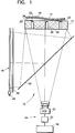
- Figure 1 shows a simple optical system 16 which can produce high finesse fringes at a CCD (charged coupled device) sensor 42 of an electronic camera 44.
- the light source 46 for this system 16 is preferably a neon discharge tube of the type normally used for optical testing of polished surfaces. These discharge lamps 46 emit light over a narrow band at 5493 ⁇ and can be formed into a large area lamp by folding a long discharge tube.
- the light source 46 could be a He-Ne laser a laser diode or a narrow band filtered light source of any desired type depending upon the source coherency requirements.
- U.S. Patent Number 5,291,269 to the present inventor, illustrates a suitable light source and is specifically incorporated by reference herein. Typically the coherence length should be sufficient only to cause fringes to be created in the gap 18 and not by other optical surfaces in the chuck 12.
- a ground glass screen 48 in front of the lamp 46 creates a large extended source which is used to illuminate the chuck 12/residual gap 18/semiconductor wafer 14 structure by means of a beamsplitter 50 which preferably comprises a piece of uncoated glass or it may be partially silvered. However, any desired beam splitter as are known in the art could be used.
- the light from the source 46 is reflected by the beam splitter 50 through the glass of the chuck 12 and the residual air gap 18 until it reaches the surface 22 of the silicon wafer 14. Reflections from the surface 22 of the silicon wafer 14 and the surface 26 of the chuck 12 result in a Fizeau fringe pattern if there is any residual air gap 18.
- the gap 18 would be a vacuum and an electrostatic chuck 24 would be used in place of the vacuum chuck 12.
- the gas in the gap 18 in this embodiment is described as being air it could be any desired gas including inert gases such as argon etc. or reactive gases used for deposition or diffusion etc.
- An image of the fringes, if any, in the gap 18 is recorded through the rear surface 30 of the chuck 12 by a CCD sensor 42 of an electronic camera 44 further including frame grabber 52 (digitizing circuit for the video image from camera 44) and computer system 54.
- the computer 54 receives the output of the electronic camera 44 and checks for the existence of fringes such as Fizeau fringes in the image of the gap 18.
- the optical system 16 shown in Figure 1 is preferably in the nature of a Fizeau interferometer.
- optical systems 16 as are known in the art can be used to record the fringes, as for example, those disclosed in the present inventors earlier patents which have been incorporated by reference herein. These also include line and point scanning systems where data is obtained in a more sequential manner by either moving the wafer 14/chuck 12 unit under a light beam or by optically scanning a light beam across the wafer 14/chuck 12 interface at high speed. Even conventional photography could be employed to photograph the fringe pattern in the gap 18 through the chuck 12 which photograph can then be examined to determine if fringes are present as well as their number and magnitude. While the interferometer 16 is preferably of a Fizeau design any desired interferometer as are known in the art could be used to generate a fringe pattern indicative of the gap 18 between the wafer 14 and the chuck 12.
- the vacuum chuck 12 configuration in the example of Figures 1 and 2 consists of a glass/air/silicon Fizeau interferometer where the reflectance varies as the air space is varied. Averaging the reflectance over the narrow band illumination accounts for coherence effects in the measurements.
- the configuration also consists of a glass/air/silicon Fizeau interferometer, with the addition of other layers due to the EC layer 32 or 36 and 38, and the top insulating layer 34 bonded thereto.
- the reflectance in these electrostatic embodiments depends upon the specific film thicknesses as well as the spectral width (coherence length effects) of the illuminating radiation. In general over a narrow band this simply leads to a reflectance offset and does not compromise the measurement of the fringes. Variations in the gap 18 thickness still primarily modulate the reflected light.
- Figure 5 shows the variation in reflectance for the basic Fizeau image having unequal amplitude reflectance at the two surfaces 20 and 22 surrounding the gap 18 being measured.
- a digitized image of the gap 18 provided as an output of the camera 44 can be used to determine the existence of fringes in several ways.
- First an estimate of the "volume of fringes" can be found by computing a merit function.
- the reflectance at any point is normalized to remove any variations in illumination uniformity U(x,y) and a merit function is computed in accordance with the following equation: where K is the total number of points in the image, R(x,y) is the spacial reflectance and R theory (x,y) is the computed reflectance for the case where the gap 18 is zero.
- Table I shows reflectance and merit function values for 4096 points in an image of a glass/air/silicon Fizeau fringe pattern for various gap thicknesses, and indicates the sensitivity of the method of this invention.
- a second method which is a sensitive measure of the existence of fringes is to compute a merit function which is the sum of nearest neighbor slopes i.e. where K is the total number of points in the image, R(x,y) is the spatial reflectance and U(x,y) is the illumination intensity.
- the above identified equations can be easily programmed for solution with a computer 54 in a conventional manner.
- the digital output of the electronic camera 44 can then be fed directly into the computer 54 to provide the necessary variable input data to compute the respective merit functions based on fringe volume and/or nearest neighbor slopes.
- fringes in the gap 18 indicate that the chuck has not succeeded in pulling the wafer completely down to conform it to the chuck 12 or 24 surface as preferred.
- the apparatus 10 of this invention can also be used with the metrology instrument of the present inventors U.S. Patent Application (Attorneys Docket No. 016-945250-NA) filed of even date herewith, which measures the thickness map of a semiconductor wafer by measuring the gaps on both sides of the wafer when it is placed between two optical flats one of which is preferably a chuck 12 or 24.
- the chuck 12 or 24 forces the gap 18 between the wafer and the chuck to be zero or to be some small fraction of a wave and allows the semiconductor wafer thickness to be measured by simply measuring the gap between the top of the wafer and the optical flat opposed thereto. By subtracting this later gap which is measured using a multispectral oblique incidence interferometer from the total chuck/optical flat separation the thickness of the wafer can be measured or a thickness map generated.
- Wafer fabrication refers to the processing of a semiconductor wafer through various photolithography, deposition, diffusion steps or the like for the purpose of creating electronic devices and circuits.
Abstract
A transparent chuck (12) is used to force a semiconductor wafer (14) to take a prescribed shape. Any gap (18) which is formed between the chuck and the wafer can be imaged through the transparent chuck. An interferometer (16) is used to illuminate the gap with a narrow band illumination to create interference fringes in the gap. The fringes can be electronically imaged to create a digital input to a computer (54). Merit functions corresponding to the total volume of fringes in the gap or to the summation of nearest neighbor slopes of such fringes provide a measure of the thickness of such gap.
Description
- The present invention relates to a chuck which is used to force a semiconductor wafer to take a prescribed shape and the process of using it. The chuck allows optical monitoring of the residual air space between the rear surface of the wafer and the front surface of the chuck using an interferometric optical system.
- Current chucks used to flatten wafers in metrology systems or in stepper machines have no way of monitoring if the chuck actually causes the wafer to conform exactly to the chuck surface without leaving an air space. Previously this error was ignored since the thickness variations in silicon wafers could be as high as 25 microns. The development of AccuFlat™ wafers by Hughes Danbury Optical Systems, Inc., Danbury, Connecticut, in which the wafer surfaces are highly parallel requires improved chucks which can pull down a wafer so as to leave an air space much less than the wafer thickness tolerance of 0.1 micron.
- Chucks used to shape a wafer to a prescribed form must be capable of operating in either air or vacuum and these requirements have lead to the commercial development of vacuum chucks as well as electrostatic chucks. Both vacuum chucks and electrostatic wafer chucks which are commercially available have opaque bodies and do not allow any measurement of how well the wafer is shaped to the chuck surface.
- Vacuum chucks initially used waffle iron or bed of nails patterns on the chuck surface in an attempt to reduce the area of the chuck in contact with the wafer. This was done to minimize the trapping of dust particles between the wafer and the chuck surface. These types of designs suffer from print through of the chuck surface pattern onto the top surface of the wafer. This was not a severe problem before the availability of AccuFlat™ wafers since the older wafers had huge thickness variations on the order of tens of microns.
- Electrostatic chucks are large area capacitors in which the electrodes can either be a single plane at high voltage separated from the grounded wafer by an insulating layer such as Kapton™, manufactured by DuPont or a multiple type where alternate metal electrodes are maintained at two different high potentials (plus and minus several hundred volts) and separated from the wafer by an insulating layer. In the latter case the wafer does not require deliberate grounding to be part of the electrostatic circuit.
- This invention consists of a new type of chuck which is used to force a semiconductor wafer, such as a silicon wafer, to take a prescribed shape. The chuck is transparent and its surface is usually polished optically flat to a fine tolerance but it can also be a substrate having an optically polished surface in the form of a sphere, parabola, ellipse or toroid or any other desired shape to provide correspondingly shaped wafer surfaces The principal difference between the chuck of this invention and those used in the prior art is that the new chuck body is transparent. The apparatus of this invention uses an interferometric optical system to provide optical monitoring of fringes in the residual air space between the rear surface of the wafer and the opposing surface of the transparent chuck.
- The wafer is forced to assume the shape of the chuck surface by using either a vacuum or an electrostatic field and either type can be configured such that the residual fringe pattern can be monitored through the transparent chuck. In the case of a vacuum chuck, the surface is preferably made from glass and small holes less than the wafer thickness are used to create vacuum paths below the wafer. In the electrostatic case, the fringes are viewed through the base electrode which is preferably fabricated from a transparent electrically conductive film (hereinafter referred to as an EC film) coated or applied onto a glass substrate, or a metal grid imbedded in the chuck or a hybrid EC film with grids embedded in the chuck to lower the electrode resistance further.
- The optical system preferably uses a single optical wavelength from a He-Ne laser, laser diode, a discharge lamp or filtered white light source to create interference fringes which are recorded by an electronic camera. In accordance with the process of this invention the recorded image is analyzed to provide merit functions which describe the closeness of fit between the wafer and the chuck. The merit functions approach zero when the wafer and chuck are exactly same shape and there is no residual air space.
In accordance with this invention a simple optical measurement is made of the air space at the junction between the adjacent chuck top surface and the opposing or rear surface of the semiconductor wafer. The air space is illuminated through the transparent chuck by a single narrow band light source of preferably a Fizeau interferometer. An electronic camera records a CCD (charged coupled device) image of the fringes which are formed in the residual air space between the chuck surface and the opposing polished or lapped surface of the semiconductor wafer. This CCD fringe pattern is then analyzed to determine if the chuck and wafer are in perfect contact. Merit functions proportional to the total fringe volume or to a summation of nearest neighbor slopes will be zero if the wafer conforms to the chuck, i.e. there will be no fringes and no detectable slopes across the image other than residual noise slopes. The measured merit functions provide a measurement of the magnitude of the residual air space or gap. - A further application of the chuck and process of this invention is the use of these chucks in steppers, particularly those which use the AccuFlat™ wafers. In accordance with this invention one can measure the wafer/chuck conformity to less than the depth of focus of a UV stepper.
- The foregoing aspects and other features of the invention are explained in the following description, taken in connection with the accompanying drawings, wherein:
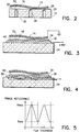
- Figure 1 is a schematic view of an apparatus in accordance with this invention comprising a vacuum chuck supporting a semiconductor wafer and an optical system for illuminating the gap between the chuck and the wafer and for digitizing an image of the fringes localized in the gap;
- Figure 2 is a side sectional view of vacuum chuck in accordance with one embodiment of this invention, supporting a semiconductor wafer;
- Figure 3 is a side sectional view of a monopole electrostatic chuck in accordance with another embodiment of this invention, supporting a semiconductor wafer;
- Figure 4 is a side sectional view of a multipole electrostatic chuck in accordance with yet another embodiment of this invention, supporting a semiconductor wafer;
- Figure 5 is a graph showing the relationship between fringe reflectance and the thickness of the gap or air space between the chuck and the wafer.
- Referring to Figure 1 there is shown an
apparatus 10 in accordance with one embodiment of this invention comprising atransparent chuck 12 supporting asemiconductor wafer 14 such as a silicon wafer and anoptical system 16 for forming and monitoring interferometric fringes in theresidual gap 18 between thefirst surface 20 of thechuck 12 and the opposingfirst surface 22 of thewafer 14. Thewafer 14 can be supported on such achuck 12 at various stages in semiconductor wafer fabrication including, for example, photolithography in a stepper, deposition or diffusion steps. While avacuum chuck 12 is shown thetransparent chuck 12 of this invention may be of any desired design so long as it is transparent. - Chucks 12 used to shape a
wafer 14 to a prescribed form must be capable of operating in air or vacuum and these requirements have lend to the commercial development ofvacuum chucks 12 as well aselectrostatic chucks 24 as will be described later by reference to Figures 3 and 4. - In the embodiment of Figures 1 and 2 the driving force is a vacuum but this type of
chuck 12 is limited to asystem 10 which can operate in air.Vacuum chucks 12 initially used waffle iron or bed of nails patterns on the chuck surface in an attempt to reduce the area of thechuck 12 in contact with thewafer 14. This was done to minimize the trapping of dust particles between thewafer surface 22 and thechuck surface 20. These types of designs suffer from print through of the chuck surface pattern onto the top surface of the wafer. This was not a severe problem whenwafers 14 had huge thickness variations of the order of tens of microns but it is a problem with AccuFlat™ wafers 14 which have small thickness variations. - Vacuum designs in accordance with this invention attempt to minimize print-through problems by using a transparent optically polished
surface 20 in which small holes 26 (less than the wafer thickness of about 600 microns) are drilled into the polishedsurface 20 to allow the vacuum path to exhaust the air in thegap 18 between the polishedsurface 20 and thesurface 22 of thewafer 14. The pattern oftiny holes 26 does not interfere with the air space orresidual gap 18 measurement since the total area of theholes 26 is extremely small compared with thewafer 14 area. - In order to provide an optically polished
surface 20 thechuck 12 is preferably formed out of a glass substrate, however any desired transparent material could be used. Theholes 26 preferably are arranged about the entire surface of thechuck 12. The inter-hole spacing is preferably on the order of thewafer 14 thickness (i.e. about 600 microns). If for example, the inter-hole spacing is about 1 millimeter a 200millimeter chuck 12 could require as many as 40,000holes 26. Such a large number ofhoes 26 would be difficult to drill, however they could be formed by any desired technique known in the art, including photolithography and etching, laser machining or the like. Theholes 26 are preferably from about 300 to about 500 microns in diameter and are laser machined into thesurface 20 in any desired pattern. In order to minimize pressure drops larger diameter countersunk or coredholes 28 are machined into the opposingsecond surface 30 of thechuck 12, in a generally coaxial relationship to theholes 26, by any desired technique, such as the use of a laser. A suitable vacuum source (not shown), such as a pump, is connected in a conventional manner to thecountersunk holes 28 either through the use of individual conduits (not shown) connected to each of theholes 28 or through the use of a suitable plenum (not shown) connected to thesurface 30 and to the vacuum source. - Referring now to Figures 3 and 4
electrostatic chucks 24 are shown which can be employed in theapparatus 10 of Figure 1 as a substitute for thevacuum chuck 12 shown therein. Thechucks 24 comprise large area capacitors in which the electrodes can either be asingle plane electrode 32 at a high or other desired voltage separated from the grounded wafer by aninsulating layer 34 such as Kapton™ or glass or other material as desired, or a multiple electrode type wherealternate metal electrodes wafer 14 by aninsulating layer 34. In the latter case thewafer 14 does not require deliberate grounding to be part of the electrostatic circuit. The voltages which are used are sufficient to force thewafer 14 into substantial conformity with thechuck surface 40. Conventional electrostatic chucks use potential differences of hundreds of volts, however a design in accordance with this a preferred embodiment of this invention can reduce the necessary potential difference to less than about 100 volts. - The electrostatic chuck deigns 24 in accordance with this invention based upon a transparent substrate require that the
metal electrode structures chuck 24 or an EC/immersed grid hybrid structure can be embedded therein. It is possible in accordance with this invention to provide extremely efficient 1 ohm/square conductive coatings which transmit >80% in the visible region. Electrostatic chucks fabricated using electrically conductive films or coatings are thus compatible with the fringevolume measurement system 10 of this invention since the silicon/air/glass interface can be viewed optically through the EC film or coating. - The Kapton™ dielectric layer could alternatively be any desired high strength dielectric material such as, for example, boron nitride, fused silica, aluminum oxide, silicon, etc. For example, an electrically conductive coating was deposited by evaporation in a vacuum and overcoated with a thin (about 0. 1 micron) layer of aluminum oxide. Although the aluminum oxide layer was slightly porous due to being deposited by evaporation using an electron beam gun, the voltage needed to pull down a large part of a
wafer 14 was only 30 to 40 volts. This compares with much higher voltages of 700 to 800 volts required by current commercial chucks which use a much thicker Kapton™ layer on the order of 25 to 50 microns thick. - Referring now to Figure 3 a
transparent chuck 24 design having amonopole electrode 32 is shown. In the chuck 24 a capacitor is formed by the continuous layer of electricallyconductive film 32 and the groundedwafer 14. Biasing theEC layer 32 at voltages up to about 1 KV with thewafer 14 grounded causes thewafer 14 to be pulled against thechuck 24surface 40 by electrostatic forces. - Referring now to Figure 4 a
transparent chuck 24 design having amultiple electrode alternate electrodes electrodes electrodes wafer 14 to be pulled against thechuck 24surface 40 without requiring that thewafer 14 be grounded as part of the electrostatic circuit. The electrostatic chucks 24 of Figures 3 and 4 are not limited to metrology orwafer fabrication systems 10 which operate in air as is the case for vacuum chucks 12. - In accordance with this invention a preferred embodiment of an
electrostatic chuck 24 can be constructed as follows. A high dielectric breakdown bulk transparent material such as boron nitride or fused silica or other desired material is ground or polished down by standard techniques for two sided polishing. The polishing is preferably carried out by plasma-assisted chemical etching to a thickness of less than about 15 microns and preferably about 10 microns or less. After polishing the dielectric material preferably is a free standing film ormembrane 34 which is capable of being handled so that it can be vacuum coated. One side of themembrane 34 is now coated (as by vapor deposition or other desired technique) with an electrically conductingfilm 32 of about 1 to 2 ohm/square electrical resistance. Alternatively a metal grid 32 (typically gold or any other desired material) wherein the grid squares are preferably several hundred microns (i.e. greater than about 400 microns and preferably greater than about 500 microns) in dimension and the grid lines are preferably about 30 to about 50 microns wide can be coated or deposited on themembrane 34. The grid allows most of the light to pass through so that an interferometric measurement of the air space orgap 18 can be made. - The
membrane 34 coated with the electrically conductive film orgrid 32 is cemented (or affixed by any desired means) to a fused silica, glass or other desired transparent material substrate or chuck 24 using optical cement or any other desired technique for adhering themembrane 34 to thechuck 24. The electrically conductive coating ormetal grid 32 is sealed between themembrane 34 and the massive transparent substrate ofchuck 24. At this point theouter surface 40 of themembrane 34 which is adapted to support thewafer 14 is not optically flat even though thesurface 20 of the massive substrate or chuck 24 is flat. This is the case since the optical cement layer can have thickness variations and the two sided polishing of themembrane 34 does not provide a totally parallel thin slab. - Fortunately the surface figure of the
top surface 40 can be measured by conventional interferometry if the deviation is less than a 1/2 wave. If thetop surface 40 deviation is more than about 1/2 wave then one can use a multispectral thin film mapper, such as the one described in U.S. Patent Number 5,333,049, to the inventor herein, which patent is specifically incorporated by reference herein, to measure thesurface 40 deviation. This is accomplished by using the mapper to measure the air gap between thesurface 40 and a known optical flat to provide a surface map. Thesurface 40 is then flattened by conventional polishing or preferably through the use of plasma assisted chemical etching techniques as are known in the art. Numerous patents assigned to Hughes Aircraft Company, the assignee of the present invention, describe plasma-assisted chemical etching (PACE) for producing thin uniform films. The PACE process can be used to thin themembrane 34 and to flatten itssurface 40. This method of constructing anelectrostatic chuck 24 has the potential to produce electrostatic chucks which operate at lower voltages, (i.e. 50 instead of 800). Accordingly in accordance with this embodiment theelectrostatic chuck 24 is capable of operating at less than about 200 volts and preferably less than about 100 volts potential drop. - Referring again to Figure 1 the
optical system 16 requires that thesemiconductor wafer 14surface 22 being viewed be polished or finely lapped to increase the reflectance, compared with the coarse ground surfaces normally found on silicon wafers. It is possible that even ground surfaces can be used to form fringes if oblique incidence illumination is used. One can obtain fringes between ground surfaces and polished surfaces but the fringe quality (maximum to minimum ratio) depends critically upon the surface roughness of the ground surface. To obtain fringes at normal incidence the surface needs to be lapped to a surface roughness in the region of a tenth of a micron. Conventional ground surfaces such as are found on the back surface of a silicon wafer are much rougher than this and therefore require that a high incidence angle be used The effects of surface roughness decrease as the incidence angle increases. - Figure 1 shows a simple
optical system 16 which can produce high finesse fringes at a CCD (charged coupled device)sensor 42 of anelectronic camera 44. Thelight source 46 for thissystem 16 is preferably a neon discharge tube of the type normally used for optical testing of polished surfaces. Thesedischarge lamps 46 emit light over a narrow band at 5493Å and can be formed into a large area lamp by folding a long discharge tube. Thelight source 46 could be a He-Ne laser a laser diode or a narrow band filtered light source of any desired type depending upon the source coherency requirements. U.S. Patent Number 5,291,269, to the present inventor, illustrates a suitable light source and is specifically incorporated by reference herein. Typically the coherence length should be sufficient only to cause fringes to be created in thegap 18 and not by other optical surfaces in thechuck 12. - A
ground glass screen 48 in front of thelamp 46 creates a large extended source which is used to illuminate thechuck 12/residual gap 18/semiconductor wafer 14 structure by means of abeamsplitter 50 which preferably comprises a piece of uncoated glass or it may be partially silvered. However, any desired beam splitter as are known in the art could be used. In this example the light from thesource 46 is reflected by thebeam splitter 50 through the glass of thechuck 12 and theresidual air gap 18 until it reaches thesurface 22 of thesilicon wafer 14. Reflections from thesurface 22 of thesilicon wafer 14 and thesurface 26 of thechuck 12 result in a Fizeau fringe pattern if there is anyresidual air gap 18. If theapparatus 10 is employed with a vacuum system thegap 18 would be a vacuum and anelectrostatic chuck 24 would be used in place of thevacuum chuck 12. Similarly while the gas in thegap 18 in this embodiment is described as being air it could be any desired gas including inert gases such as argon etc. or reactive gases used for deposition or diffusion etc. - An image of the fringes, if any, in the
gap 18 is recorded through therear surface 30 of thechuck 12 by aCCD sensor 42 of anelectronic camera 44 further including frame grabber 52 (digitizing circuit for the video image from camera 44) andcomputer system 54. Thecomputer 54 receives the output of theelectronic camera 44 and checks for the existence of fringes such as Fizeau fringes in the image of thegap 18. Theoptical system 16 shown in Figure 1 is preferably in the nature of a Fizeau interferometer. - Numerous other
optical systems 16 as are known in the art can be used to record the fringes, as for example, those disclosed in the present inventors earlier patents which have been incorporated by reference herein. These also include line and point scanning systems where data is obtained in a more sequential manner by either moving thewafer 14/chuck 12 unit under a light beam or by optically scanning a light beam across thewafer 14/chuck 12 interface at high speed. Even conventional photography could be employed to photograph the fringe pattern in thegap 18 through thechuck 12 which photograph can then be examined to determine if fringes are present as well as their number and magnitude. While theinterferometer 16 is preferably of a Fizeau design any desired interferometer as are known in the art could be used to generate a fringe pattern indicative of thegap 18 between thewafer 14 and thechuck 12. - The
vacuum chuck 12 configuration in the example of Figures 1 and 2 consists of a glass/air/silicon Fizeau interferometer where the reflectance varies as the air space is varied. Averaging the reflectance over the narrow band illumination accounts for coherence effects in the measurements. In the case of theelectrostatic chuck 24 embodiments of Figures 3 and 4, the configuration also consists of a glass/air/silicon Fizeau interferometer, with the addition of other layers due to theEC layer layer 34 bonded thereto. The reflectance in these electrostatic embodiments depends upon the specific film thicknesses as well as the spectral width (coherence length effects) of the illuminating radiation. In general over a narrow band this simply leads to a reflectance offset and does not compromise the measurement of the fringes. Variations in thegap 18 thickness still primarily modulate the reflected light. - Figure 5 shows the variation in reflectance for the basic Fizeau image having unequal amplitude reflectance at the two
surfaces gap 18 being measured. A digitized image of thegap 18 provided as an output of thecamera 44 can be used to determine the existence of fringes in several ways. First an estimate of the "volume of fringes" can be found by computing a merit function. The reflectance at any point is normalized to remove any variations in illumination uniformity U(x,y) and a merit function is computed in accordance with the following equation:
where K is the total number of points in the image, R(x,y) is the spacial reflectance and Rtheory(x,y) is the computed reflectance for the case where thegap 18 is zero. If thechuck wafer 14 to thechuck surface 20 then thegap 18 will approach zero and the above merit function will rapidly approach zero. Table I shows reflectance and merit function values for 4096 points in an image of a glass/air/silicon Fizeau fringe pattern for various gap thicknesses, and indicates the sensitivity of the method of this invention.

- Reference to Figure 5 indicates that the measurement becomes ambiguous after a half wave of optical thickness is reached in that the values repeat. This is not expected to be a problem since one can assume that the
chuck residual gap 18 to less than a half wave. - A second method which is a sensitive measure of the existence of fringes is to compute a merit function which is the sum of nearest neighbor slopes i.e.

where K is the total number of points in the image, R(x,y) is the spatial reflectance and U(x,y) is the illumination intensity. - This function will also approach zero as fringes disappear. Note that this approach does not require a knowledge of the zero thickness air space reflectance.
- The above identified equations can be easily programmed for solution with a
computer 54 in a conventional manner. The digital output of theelectronic camera 44 can then be fed directly into thecomputer 54 to provide the necessary variable input data to compute the respective merit functions based on fringe volume and/or nearest neighbor slopes. - In all cases, fringes in the
gap 18 indicate that the chuck has not succeeded in pulling the wafer completely down to conform it to thechuck - The
apparatus 10 of this invention can also be used with the metrology instrument of the present inventors U.S. Patent Application (Attorneys Docket No. 016-945250-NA) filed of even date herewith, which measures the thickness map of a semiconductor wafer by measuring the gaps on both sides of the wafer when it is placed between two optical flats one of which is preferably achuck chuck gap 18 between the wafer and the chuck to be zero or to be some small fraction of a wave and allows the semiconductor wafer thickness to be measured by simply measuring the gap between the top of the wafer and the optical flat opposed thereto. By subtracting this later gap which is measured using a multispectral oblique incidence interferometer from the total chuck/optical flat separation the thickness of the wafer can be measured or a thickness map generated. - Wafer fabrication as the term is used herein refers to the processing of a semiconductor wafer through various photolithography, deposition, diffusion steps or the like for the purpose of creating electronic devices and circuits.
- It should be understood that the foregoing description is only illustrative of the invention. Various alternatives and modifications can be devised by those skilled in the art without departing from the spirit of the invention.
- Accordingly, the present invention is intended to embrace all such alternatives, modifications and variations which fall within the scope of the appended claims.
Claims (10)
- A chuck for supporting a semiconductor wafer during wafer fabrication comprising:
a transparent substrate having an optically polished surface of a desired shape for supporting said wafer;
a system for securing said wafer over said polished surface so that said wafer substantially conforms thereto;
said substrate being sufficiently transparent to permit any gap which may form between said polished surface and said wafer to be optically imaged through said substrate. - A chuck as in claim 1 wherein said substrate is sufficiently transparent to allow a narrow band illumination to form interference fringes in said gap and to allow the optical imaging of such fringes.
- A chuck as in claim 2 wherein said securing system comprises a system for applying a vacuum to said gap through said substrate.
- A chuck as in claim 2 wherein said securing system comprises a system for applying an electrostatic force on said wafer to force it into engagement over said polished surface.
- A chuck as in claim 4 wherein said system for applying said electrostatic force comprises:1) a monopole electrode on said polished surface of said substrate;2) an insulating layer over said monopole electrode for spacing said electrode from said wafer by a desired amount;3) said wafer and said monopole electrode being adapted to have a potential drop of sufficient magnitude created between them to provide said electrostatic force; and4) said monopole electrode and said insulating layer being sufficiently transparent to allow a narrow band illumination to form interference fringes in said gap and to allow the optical imaging of such fringes.
- A chuck as in claim 4 wherein said system for applying said electrostatic force comprises:1) a multipole electrode on said polished surface of said substrate, said multipole electrode comprising alternating electrode members of opposing polarity;2) an insulating layer over said multipole electrode for spacing said electrode from said wafer by a desired amount;3) said electrode members being adapted to have a potential drop of sufficient magnitude created between them to create said electrostatic force;4) said multipole electrode and said insulating layer being sufficiently transparent to allow a narrow band illumination to form interference fringes in said gap and to allow the optical imaging of such fringes.
- An apparatus for monitoring a residual gap between a semiconductor wafer and a chuck for supporting said semiconductor wafer comprising:
a transparent chuck having a surface of a desired shape for supporting said wafer;
a wafer supported over said chuck surface such that a first surface of said wafer opposes said chuck surface;
said residual gap being defined between said first surface of said wafer and said chuck surface;
a narrow band illumination source arranged to illuminate said gap through said transparent chuck, said illumination being selected to form interference fringes in said gap indicative of the thickness of said gap; and a camera for creating an image of said interference fringes. - An apparatus as in claim 7 wherein said camera is an electronic camera including a charged coupled device imaging system providing a digital output corresponding to said fringes in said gap and wherein said apparatus further includes a computer for receiving said output, said computer being adapted to calculate a merit function proportional to the total fringe volume.
- An apparatus as in claim 7 wherein said camera is an electronic camera including a charged coupled device imaging system providing a digital output corresponding to said fringes in said gap and wherein said apparatus further includes a computer for receiving said output, said computer being adapted to calculate a merit function proportional to a summation of nearest neighbor slopes of said fringes.
- An apparatus as in claim 7 wherein said illumination source is part of a Fizeau interferometer system further comprising a beam splitter arranged between said chuck and said camera and wherein said illumination source is arranged to illuminate said gap by reflection off said beam splitter.
Applications Claiming Priority (2)
| Application Number | Priority Date | Filing Date | Title |
|---|---|---|---|
| US304984 | 1994-09-13 | ||
| US08/304,984 US5515167A (en) | 1994-09-13 | 1994-09-13 | Transparent optical chuck incorporating optical monitoring |
Publications (1)
| Publication Number | Publication Date |
|---|---|
| EP0706210A1 true EP0706210A1 (en) | 1996-04-10 |
Family
ID=23178796
Family Applications (1)
| Application Number | Title | Priority Date | Filing Date |
|---|---|---|---|
| EP95306424A Withdrawn EP0706210A1 (en) | 1994-09-13 | 1995-09-13 | Transparent optical chuck incorporating optical monitoring |
Country Status (5)
| Country | Link |
|---|---|
| US (1) | US5515167A (en) |
| EP (1) | EP0706210A1 (en) |
| JP (1) | JPH08181199A (en) |
| KR (1) | KR960012420A (en) |
| IL (1) | IL115230A0 (en) |
Cited By (18)
| Publication number | Priority date | Publication date | Assignee | Title |
|---|---|---|---|---|
| EP1432546A1 (en) * | 2001-08-31 | 2004-06-30 | Cascade Microtech, Inc. | Optical testing device |
| SG111979A1 (en) * | 2001-12-03 | 2005-06-29 | Nitto Denko Corp | Semiconductor wafer transport method and semiconductor wafer transport apparatus using the same |
| EP1567913A1 (en) * | 2002-11-13 | 2005-08-31 | Molecular Imprints, Inc. | A chucking system and method for modulating shapes of substrates |
| WO2006069942A1 (en) * | 2004-12-27 | 2006-07-06 | Alphasem Ag | Device for fixing a flat object, in particular a substrate, to a work surface by means of low pressure |
| US7119346B2 (en) | 2003-11-13 | 2006-10-10 | Asml Netherlands B.V. | Lithographic apparatus and device manufacturing method |
| US7138813B2 (en) | 1999-06-30 | 2006-11-21 | Cascade Microtech, Inc. | Probe station thermal chuck with shielding for capacitive current |
| DE102006057075A1 (en) * | 2006-11-30 | 2008-06-05 | Friedrich-Schiller-Universität Jena | Chucking surface 's shape measuring method for wafer-chuck, involves reproducing mechanical contact requirements arising in chemical mechanical polishing process between wafer-chuck, backing film, wafer, polishing pad and polishing table |
| US7492172B2 (en) | 2003-05-23 | 2009-02-17 | Cascade Microtech, Inc. | Chuck for holding a device under test |
| US7656172B2 (en) | 2005-01-31 | 2010-02-02 | Cascade Microtech, Inc. | System for testing semiconductors |
| US7688062B2 (en) | 2000-09-05 | 2010-03-30 | Cascade Microtech, Inc. | Probe station |
| US7688091B2 (en) | 2003-12-24 | 2010-03-30 | Cascade Microtech, Inc. | Chuck with integrated wafer support |
| CN1726429B (en) * | 2002-11-13 | 2010-10-13 | 分子制模股份有限公司 | Chucking system and method for modulating shapes of substrates |
| US7898281B2 (en) | 2005-01-31 | 2011-03-01 | Cascade Mircotech, Inc. | Interface for testing semiconductors |
| US7969173B2 (en) | 2000-09-05 | 2011-06-28 | Cascade Microtech, Inc. | Chuck for holding a device under test |
| US8069491B2 (en) | 2003-10-22 | 2011-11-29 | Cascade Microtech, Inc. | Probe testing structure |
| US8319503B2 (en) | 2008-11-24 | 2012-11-27 | Cascade Microtech, Inc. | Test apparatus for measuring a characteristic of a device under test |
| WO2016034278A1 (en) * | 2014-09-05 | 2016-03-10 | Jenoptik Optical Systems Gmbh | Retaining apparatus for retaining a substrate for a treatment process, method for producing the same, and method and apparatus for monitoring a retaining plane of a retaining apparatus |
| WO2021194780A1 (en) * | 2020-03-27 | 2021-09-30 | Corning Incorporated | Substrate holder for use with interferometer |
Families Citing this family (80)
| Publication number | Priority date | Publication date | Assignee | Title |
|---|---|---|---|---|
| US5691876A (en) * | 1995-01-31 | 1997-11-25 | Applied Materials, Inc. | High temperature polyimide electrostatic chuck |
| US5644467A (en) * | 1995-09-28 | 1997-07-01 | Applied Materials, Inc. | Method and structure for improving gas breakdown resistance and reducing the potential of arcing in a electrostatic chuck |
| US5909282A (en) * | 1996-05-31 | 1999-06-01 | Tropel Corporation | Interferometer for measuring thickness variations of semiconductor wafers |
| US5932045A (en) * | 1997-06-02 | 1999-08-03 | Lucent Technologies Inc. | Method for fabricating a multilayer optical article |
| US8779322B2 (en) | 1997-06-26 | 2014-07-15 | Mks Instruments Inc. | Method and apparatus for processing metal bearing gases |
| US7569790B2 (en) * | 1997-06-26 | 2009-08-04 | Mks Instruments, Inc. | Method and apparatus for processing metal bearing gases |
| US6388226B1 (en) | 1997-06-26 | 2002-05-14 | Applied Science And Technology, Inc. | Toroidal low-field reactive gas source |
| US6815633B1 (en) | 1997-06-26 | 2004-11-09 | Applied Science & Technology, Inc. | Inductively-coupled toroidal plasma source |
| US7166816B1 (en) * | 1997-06-26 | 2007-01-23 | Mks Instruments, Inc. | Inductively-coupled torodial plasma source |
| US6150628A (en) | 1997-06-26 | 2000-11-21 | Applied Science And Technology, Inc. | Toroidal low-field reactive gas source |
| US5872694A (en) * | 1997-12-23 | 1999-02-16 | Siemens Aktiengesellschaft | Method and apparatus for determining wafer warpage for optimized electrostatic chuck clamping voltage |
| DE69930726T2 (en) * | 1998-01-12 | 2007-01-25 | Massachusetts Institute Of Technology, Cambridge | METHOD AND DEVICE FOR MICROTEST PROCESSING |
| US6063235A (en) * | 1998-08-14 | 2000-05-16 | Plasmasil, Llc | Gas discharge apparatus for wafer etching systems |
| US6334960B1 (en) | 1999-03-11 | 2002-01-01 | Board Of Regents, The University Of Texas System | Step and flash imprint lithography |
| US6437868B1 (en) * | 1999-10-28 | 2002-08-20 | Agere Systems Guardian Corp. | In-situ automated contactless thickness measurement for wafer thinning |
| US6873087B1 (en) | 1999-10-29 | 2005-03-29 | Board Of Regents, The University Of Texas System | High precision orientation alignment and gap control stages for imprint lithography processes |
| US7432634B2 (en) * | 2000-10-27 | 2008-10-07 | Board Of Regents, University Of Texas System | Remote center compliant flexure device |
| EP1303792B1 (en) | 2000-07-16 | 2012-10-03 | Board Of Regents, The University Of Texas System | High-resolution overlay alignement methods and systems for imprint lithography |
| EP2270592B1 (en) * | 2000-07-17 | 2015-09-02 | Board of Regents, The University of Texas System | Method of forming a pattern on a substrate |
| US7479456B2 (en) * | 2004-08-26 | 2009-01-20 | Applied Materials, Inc. | Gasless high voltage high contact force wafer contact-cooling electrostatic chuck |
| US8016277B2 (en) * | 2000-08-21 | 2011-09-13 | Board Of Regents, The University Of Texas System | Flexure based macro motion translation stage |
| JP2004523906A (en) | 2000-10-12 | 2004-08-05 | ボード・オブ・リージエンツ,ザ・ユニバーシテイ・オブ・テキサス・システム | Templates for room-temperature and low-pressure micro and nano-transfer lithography |
| US20050274219A1 (en) * | 2004-06-01 | 2005-12-15 | Molecular Imprints, Inc. | Method and system to control movement of a body for nano-scale manufacturing |
| US6964793B2 (en) * | 2002-05-16 | 2005-11-15 | Board Of Regents, The University Of Texas System | Method for fabricating nanoscale patterns in light curable compositions using an electric field |
| US6721076B2 (en) | 2001-08-03 | 2004-04-13 | Inphase Technologies, Inc. | System and method for reflective holographic storage with associated multiplexing techniques |
| US7112359B2 (en) * | 2001-08-22 | 2006-09-26 | Inphase Technologies, Inc. | Method and apparatus for multilayer optical articles |
| US7001541B2 (en) * | 2001-09-14 | 2006-02-21 | Inphase Technologies, Inc. | Method for forming multiply patterned optical articles |
| US6825960B2 (en) * | 2002-01-15 | 2004-11-30 | Inphase Technologies, Inc. | System and method for bitwise readout holographic ROM |
| US7077992B2 (en) * | 2002-07-11 | 2006-07-18 | Molecular Imprints, Inc. | Step and repeat imprint lithography processes |
| US6932934B2 (en) * | 2002-07-11 | 2005-08-23 | Molecular Imprints, Inc. | Formation of discontinuous films during an imprint lithography process |
| US7071088B2 (en) * | 2002-08-23 | 2006-07-04 | Molecular Imprints, Inc. | Method for fabricating bulbous-shaped vias |
| US8349241B2 (en) | 2002-10-04 | 2013-01-08 | Molecular Imprints, Inc. | Method to arrange features on a substrate to replicate features having minimal dimensional variability |
| US7641840B2 (en) * | 2002-11-13 | 2010-01-05 | Molecular Imprints, Inc. | Method for expelling gas positioned between a substrate and a mold |
| US6980282B2 (en) * | 2002-12-11 | 2005-12-27 | Molecular Imprints, Inc. | Method for modulating shapes of substrates |
| US6871558B2 (en) * | 2002-12-12 | 2005-03-29 | Molecular Imprints, Inc. | Method for determining characteristics of substrate employing fluid geometries |
| US7452574B2 (en) * | 2003-02-27 | 2008-11-18 | Molecular Imprints, Inc. | Method to reduce adhesion between a polymerizable layer and a substrate employing a fluorine-containing layer |
| DE10331565A1 (en) * | 2003-05-28 | 2004-12-30 | Osram Opto Semiconductors Gmbh | Wafer holding device for semiconductor chips in wafers has holed suction device on vacuum chamber that is transparent to electromagnetic radiation |
| US20050106321A1 (en) * | 2003-11-14 | 2005-05-19 | Molecular Imprints, Inc. | Dispense geometery to achieve high-speed filling and throughput |
| US8084866B2 (en) | 2003-12-10 | 2011-12-27 | Micron Technology, Inc. | Microelectronic devices and methods for filling vias in microelectronic devices |
| US7091124B2 (en) | 2003-11-13 | 2006-08-15 | Micron Technology, Inc. | Methods for forming vias in microelectronic devices, and methods for packaging microelectronic devices |
| US8076386B2 (en) | 2004-02-23 | 2011-12-13 | Molecular Imprints, Inc. | Materials for imprint lithography |
| US7906180B2 (en) * | 2004-02-27 | 2011-03-15 | Molecular Imprints, Inc. | Composition for an etching mask comprising a silicon-containing material |
| US20050247894A1 (en) | 2004-05-05 | 2005-11-10 | Watkins Charles M | Systems and methods for forming apertures in microfeature workpieces |
| WO2005119802A2 (en) * | 2004-05-28 | 2005-12-15 | Board Of Regents, The University Of Texas System | Adaptive shape substrate support system and method |
| TWI242255B (en) * | 2004-07-21 | 2005-10-21 | Touch Micro System Tech | Wafer carrier |
| SG120200A1 (en) | 2004-08-27 | 2006-03-28 | Micron Technology Inc | Slanted vias for electrical circuits on circuit boards and other substrates |
| US7300857B2 (en) * | 2004-09-02 | 2007-11-27 | Micron Technology, Inc. | Through-wafer interconnects for photoimager and memory wafers |
| US7666464B2 (en) * | 2004-10-23 | 2010-02-23 | Applied Materials, Inc. | RF measurement feedback control and diagnostics for a plasma immersion ion implantation reactor |
| US20060145398A1 (en) * | 2004-12-30 | 2006-07-06 | Board Of Regents, The University Of Texas System | Release layer comprising diamond-like carbon (DLC) or doped DLC with tunable composition for imprint lithography templates and contact masks |
| US7798801B2 (en) * | 2005-01-31 | 2010-09-21 | Molecular Imprints, Inc. | Chucking system for nano-manufacturing |
| US7636999B2 (en) * | 2005-01-31 | 2009-12-29 | Molecular Imprints, Inc. | Method of retaining a substrate to a wafer chuck |
| US7635263B2 (en) * | 2005-01-31 | 2009-12-22 | Molecular Imprints, Inc. | Chucking system comprising an array of fluid chambers |
| US7795134B2 (en) | 2005-06-28 | 2010-09-14 | Micron Technology, Inc. | Conductive interconnect structures and formation methods using supercritical fluids |
| JP4462140B2 (en) * | 2005-07-27 | 2010-05-12 | 住友電気工業株式会社 | Wafer prober chuck top, wafer holder, and wafer prober including the same |
| US8202075B2 (en) * | 2005-08-12 | 2012-06-19 | Canon Kabushiki Kaisha | Imprint apparatus and imprint method |
| US7262134B2 (en) * | 2005-09-01 | 2007-08-28 | Micron Technology, Inc. | Microfeature workpieces and methods for forming interconnects in microfeature workpieces |
| US7622377B2 (en) * | 2005-09-01 | 2009-11-24 | Micron Technology, Inc. | Microfeature workpiece substrates having through-substrate vias, and associated methods of formation |
| US7863187B2 (en) * | 2005-09-01 | 2011-01-04 | Micron Technology, Inc. | Microfeature workpieces and methods for forming interconnects in microfeature workpieces |
| US20070045120A1 (en) * | 2005-09-01 | 2007-03-01 | Micron Technology, Inc. | Methods and apparatus for filling features in microfeature workpieces |
| US20070082179A1 (en) * | 2005-10-07 | 2007-04-12 | Wade James J | Method and apparatus for forming optical articles |
| JP5268239B2 (en) * | 2005-10-18 | 2013-08-21 | キヤノン株式会社 | Pattern forming apparatus and pattern forming method |
| US7670530B2 (en) * | 2006-01-20 | 2010-03-02 | Molecular Imprints, Inc. | Patterning substrates employing multiple chucks |
| MY144847A (en) | 2005-12-08 | 2011-11-30 | Molecular Imprints Inc | Method and system for double-sided patterning of substrates |
| US8215946B2 (en) | 2006-05-18 | 2012-07-10 | Molecular Imprints, Inc. | Imprint lithography system and method |
| US7749899B2 (en) * | 2006-06-01 | 2010-07-06 | Micron Technology, Inc. | Microelectronic workpieces and methods and systems for forming interconnects in microelectronic workpieces |
| US7629249B2 (en) | 2006-08-28 | 2009-12-08 | Micron Technology, Inc. | Microfeature workpieces having conductive interconnect structures formed by chemically reactive processes, and associated systems and methods |
| US7902643B2 (en) * | 2006-08-31 | 2011-03-08 | Micron Technology, Inc. | Microfeature workpieces having interconnects and conductive backplanes, and associated systems and methods |
| SG150410A1 (en) | 2007-08-31 | 2009-03-30 | Micron Technology Inc | Partitioned through-layer via and associated systems and methods |
| US7884015B2 (en) * | 2007-12-06 | 2011-02-08 | Micron Technology, Inc. | Methods for forming interconnects in microelectronic workpieces and microelectronic workpieces formed using such methods |
| DE102008022792A1 (en) * | 2008-05-08 | 2009-11-26 | Fraunhofer-Gesellschaft zur Förderung der angewandten Forschung e.V. | Electrostatic holding element with anti-reflection coating, measuring method and use of the holding element |
| DE102011075001A1 (en) * | 2011-04-29 | 2012-10-31 | 3D-Micromac Ag | Transmitted light vacuum chuck has light transmissive platen that is made of porous material having multiple communicating pores which form gas passage channels |
| JP6154173B2 (en) * | 2013-04-03 | 2017-06-28 | 株式会社ナノテム | Vacuum suction device and suction plate |
| KR102036907B1 (en) * | 2013-04-17 | 2019-10-28 | 삼성디스플레이 주식회사 | Metal sheet holding device for manufacturing fine metal mask |
| US9558981B2 (en) * | 2013-11-19 | 2017-01-31 | Applied Materials, Inc. | Control systems employing deflection sensors to control clamping forces applied by electrostatic chucks, and related methods |
| JP6784527B2 (en) * | 2016-07-12 | 2020-11-11 | 株式会社ディスコ | Electrostatic chuck table, laser machining equipment and machining method of workpiece |
| JP6925711B2 (en) * | 2017-04-12 | 2021-08-25 | 株式会社ディスコ | Laser machining method for frame unit and workpiece |
| JP7252322B2 (en) | 2018-09-24 | 2023-04-04 | エーエスエムエル ネザーランズ ビー.ブイ. | Process tools and inspection methods |
| JP7370265B2 (en) * | 2020-01-30 | 2023-10-27 | 株式会社ディスコ | Processing method and processing equipment |
| US11231452B2 (en) | 2020-02-04 | 2022-01-25 | Lumentum Operations Llc | Testing apparatus for optical devices |
| KR20210101983A (en) | 2020-02-11 | 2021-08-19 | 삼성전자주식회사 | Wafer inspection device and manufacturing method of semiconductor device using the same |
Citations (7)
| Publication number | Priority date | Publication date | Assignee | Title |
|---|---|---|---|---|
| JPS6436019A (en) * | 1987-07-31 | 1989-02-07 | Nippon Telegraph & Telephone | Mask adhesion device and usage of same |
| JPH01264219A (en) * | 1988-04-15 | 1989-10-20 | Hitachi Ltd | Proximity aligner |
| WO1989012318A1 (en) * | 1988-06-02 | 1989-12-14 | Hughes Aircraft Company | Optically flat surfaces on processed silicon wafers |
| US4941255A (en) * | 1989-11-15 | 1990-07-17 | Eastman Kodak Company | Method for precision multichip assembly |
| US5258236A (en) * | 1991-05-03 | 1993-11-02 | Ibm Corporation | Multi-layer thin film structure and parallel processing method for fabricating same |
| US5291269A (en) | 1991-12-06 | 1994-03-01 | Hughes Aircraft Company | Apparatus and method for performing thin film layer thickness metrology on a thin film layer having shape deformations and local slope variations |
| US5333049A (en) | 1991-12-06 | 1994-07-26 | Hughes Aircraft Company | Apparatus and method for interferometrically measuring the thickness of thin films using full aperture irradiation |
Family Cites Families (9)
| Publication number | Priority date | Publication date | Assignee | Title |
|---|---|---|---|---|
| DE2731746C2 (en) * | 1977-07-14 | 1985-08-22 | Robert Bosch Gmbh, 7000 Stuttgart | Ignition device for an internal combustion engine |
| JPS56162835A (en) * | 1980-05-19 | 1981-12-15 | Toshiba Corp | Mask matching device |
| US4932781A (en) * | 1983-11-04 | 1990-06-12 | Canon Kabushiki Kaisha | Gap measuring apparatus using interference fringes of reflected light |
| JPH03225322A (en) * | 1990-01-31 | 1991-10-04 | Ricoh Co Ltd | Recording medium |
| JPH04186654A (en) * | 1990-11-16 | 1992-07-03 | Mitsubishi Electric Corp | Boat device for manufacturing semiconductor device |
| JPH04372152A (en) * | 1991-06-20 | 1992-12-25 | Nikon Corp | Electrostatic chuck device |
| JPH05275520A (en) * | 1992-03-26 | 1993-10-22 | Fujitsu Ltd | Electrostatic attracting device and plasma treatment device |
| JPH05343507A (en) * | 1992-06-10 | 1993-12-24 | Fujitsu Ltd | Electrostatic attraction method |
| US5363171A (en) * | 1993-07-29 | 1994-11-08 | The United States Of America As Represented By The Director, National Security Agency | Photolithography exposure tool and method for in situ photoresist measurments and exposure control |
-
1994
- 1994-09-13 US US08/304,984 patent/US5515167A/en not_active Expired - Lifetime
-
1995
- 1995-09-10 IL IL11523095A patent/IL115230A0/en unknown
- 1995-09-13 KR KR1019950029818A patent/KR960012420A/en not_active Application Discontinuation
- 1995-09-13 JP JP23552795A patent/JPH08181199A/en active Pending
- 1995-09-13 EP EP95306424A patent/EP0706210A1/en not_active Withdrawn
Patent Citations (7)
| Publication number | Priority date | Publication date | Assignee | Title |
|---|---|---|---|---|
| JPS6436019A (en) * | 1987-07-31 | 1989-02-07 | Nippon Telegraph & Telephone | Mask adhesion device and usage of same |
| JPH01264219A (en) * | 1988-04-15 | 1989-10-20 | Hitachi Ltd | Proximity aligner |
| WO1989012318A1 (en) * | 1988-06-02 | 1989-12-14 | Hughes Aircraft Company | Optically flat surfaces on processed silicon wafers |
| US4941255A (en) * | 1989-11-15 | 1990-07-17 | Eastman Kodak Company | Method for precision multichip assembly |
| US5258236A (en) * | 1991-05-03 | 1993-11-02 | Ibm Corporation | Multi-layer thin film structure and parallel processing method for fabricating same |
| US5291269A (en) | 1991-12-06 | 1994-03-01 | Hughes Aircraft Company | Apparatus and method for performing thin film layer thickness metrology on a thin film layer having shape deformations and local slope variations |
| US5333049A (en) | 1991-12-06 | 1994-07-26 | Hughes Aircraft Company | Apparatus and method for interferometrically measuring the thickness of thin films using full aperture irradiation |
Non-Patent Citations (3)
| Title |
|---|
| "coverglass bonding for dirt intensive mask", IBM TECHNICAL DISCLOSURE BULLETIN, vol. 20, no. 8, January 1978 (1978-01-01), NEW YORK, pages 3000 - 3001 * |
| PATENT ABSTRACTS OF JAPAN vol. 13, no. 226 (E - 763) 25 May 1989 (1989-05-25) * |
| PATENT ABSTRACTS OF JAPAN vol. 14, no. 22 (E - 874) 17 January 1990 (1990-01-17) * |
Cited By (23)
| Publication number | Priority date | Publication date | Assignee | Title |
|---|---|---|---|---|
| US7138813B2 (en) | 1999-06-30 | 2006-11-21 | Cascade Microtech, Inc. | Probe station thermal chuck with shielding for capacitive current |
| US7688062B2 (en) | 2000-09-05 | 2010-03-30 | Cascade Microtech, Inc. | Probe station |
| US7969173B2 (en) | 2000-09-05 | 2011-06-28 | Cascade Microtech, Inc. | Chuck for holding a device under test |
| EP1432546A4 (en) * | 2001-08-31 | 2006-06-07 | Cascade Microtech Inc | Optical testing device |
| EP1432546A1 (en) * | 2001-08-31 | 2004-06-30 | Cascade Microtech, Inc. | Optical testing device |
| SG111979A1 (en) * | 2001-12-03 | 2005-06-29 | Nitto Denko Corp | Semiconductor wafer transport method and semiconductor wafer transport apparatus using the same |
| CN1726429B (en) * | 2002-11-13 | 2010-10-13 | 分子制模股份有限公司 | Chucking system and method for modulating shapes of substrates |
| EP1567913A1 (en) * | 2002-11-13 | 2005-08-31 | Molecular Imprints, Inc. | A chucking system and method for modulating shapes of substrates |
| EP1567913A4 (en) * | 2002-11-13 | 2008-08-13 | Molecular Imprints Inc | A chucking system and method for modulating shapes of substrates |
| EP2261966A3 (en) * | 2002-11-13 | 2010-12-29 | Molecular Imprints, Inc. | A chucking system to hold a substrate and a lithographic system including the chucking system |
| US7492172B2 (en) | 2003-05-23 | 2009-02-17 | Cascade Microtech, Inc. | Chuck for holding a device under test |
| US7876115B2 (en) | 2003-05-23 | 2011-01-25 | Cascade Microtech, Inc. | Chuck for holding a device under test |
| US8069491B2 (en) | 2003-10-22 | 2011-11-29 | Cascade Microtech, Inc. | Probe testing structure |
| US7119346B2 (en) | 2003-11-13 | 2006-10-10 | Asml Netherlands B.V. | Lithographic apparatus and device manufacturing method |
| US7688091B2 (en) | 2003-12-24 | 2010-03-30 | Cascade Microtech, Inc. | Chuck with integrated wafer support |
| WO2006069942A1 (en) * | 2004-12-27 | 2006-07-06 | Alphasem Ag | Device for fixing a flat object, in particular a substrate, to a work surface by means of low pressure |
| US7656172B2 (en) | 2005-01-31 | 2010-02-02 | Cascade Microtech, Inc. | System for testing semiconductors |
| US7898281B2 (en) | 2005-01-31 | 2011-03-01 | Cascade Mircotech, Inc. | Interface for testing semiconductors |
| US7940069B2 (en) | 2005-01-31 | 2011-05-10 | Cascade Microtech, Inc. | System for testing semiconductors |
| DE102006057075A1 (en) * | 2006-11-30 | 2008-06-05 | Friedrich-Schiller-Universität Jena | Chucking surface 's shape measuring method for wafer-chuck, involves reproducing mechanical contact requirements arising in chemical mechanical polishing process between wafer-chuck, backing film, wafer, polishing pad and polishing table |
| US8319503B2 (en) | 2008-11-24 | 2012-11-27 | Cascade Microtech, Inc. | Test apparatus for measuring a characteristic of a device under test |
| WO2016034278A1 (en) * | 2014-09-05 | 2016-03-10 | Jenoptik Optical Systems Gmbh | Retaining apparatus for retaining a substrate for a treatment process, method for producing the same, and method and apparatus for monitoring a retaining plane of a retaining apparatus |
| WO2021194780A1 (en) * | 2020-03-27 | 2021-09-30 | Corning Incorporated | Substrate holder for use with interferometer |
Also Published As
| Publication number | Publication date |
|---|---|
| JPH08181199A (en) | 1996-07-12 |
| US5515167A (en) | 1996-05-07 |
| IL115230A0 (en) | 1995-12-31 |
| KR960012420A (en) | 1996-04-20 |
Similar Documents
| Publication | Publication Date | Title |
|---|---|---|
| US5515167A (en) | Transparent optical chuck incorporating optical monitoring | |
| US5724144A (en) | Process monitoring and thickness measurement from the back side of a semiconductor body | |
| US7884024B2 (en) | Apparatus and method for optical interference fringe based integrated circuit processing | |
| US5661408A (en) | Real-time in-line testing of semiconductor wafers | |
| US6204922B1 (en) | Rapid and accurate thin film measurement of individual layers in a multi-layered or patterned sample | |
| CN100360895C (en) | Interferometer for measuring virtual contact surfaces | |
| JP2002517750A (en) | Apparatus and method for measuring properties of layers in a multilayer structure | |
| Brown-Hayes et al. | Towards a precision measurement of the Casimir force in a cylinder-plane geometry | |
| WO2014084574A1 (en) | Device and method for analyzing defects by using heat distribution measurement | |
| KR100345362B1 (en) | Resolving power evaluation method of electron microscope and specimen for resolving power evaluation | |
| US7642772B1 (en) | Non-contact method and apparatus for measurement of leakage current of p-n junctions in IC product wafers | |
| IL111540A (en) | Method of planarizing a microstructure | |
| KR0150416B1 (en) | Method of measuring electric charge of semiconductor wafer | |
| TWI239382B (en) | Interferometric method for endpointing plasma etch processes | |
| US6836316B2 (en) | Substrate holding apparatus and exposure apparatus using the same | |
| KR0150428B1 (en) | Non-destructive measuring sensor for semiconductor wafer and method of manufacturing the same | |
| Sakai et al. | Noncontact, electrode-free capacitance/voltage measurement based on general theory of metal-oxide-semiconductor (MOS) structure | |
| JP3814384B2 (en) | Surface position detection method and surface position detection apparatus | |
| US7050160B1 (en) | Process and apparatus for integrating sheet resistance measurements and reflectance measurements of a thin film in a common apparatus | |
| CN112992711A (en) | Method for measuring thickness of top silicon and buried oxide layer of ultra-thin SOI material | |
| US3421079A (en) | Measuring thin film thickness using interferometric-capacitance technique | |
| US11885609B2 (en) | Wafer thickness, topography, and layer thickness metrology system | |
| JP2000208448A (en) | Method and apparatus for manufacturing circuit board | |
| CN115110050A (en) | Method for preparing ultrathin coplanar waveguide with communicated front and back surfaces on diamond surface | |
| JPH01293518A (en) | Aligner having device for detecting variation of height of substrate |
Legal Events
| Date | Code | Title | Description |
|---|---|---|---|
| PUAI | Public reference made under article 153(3) epc to a published international application that has entered the european phase |
Free format text: ORIGINAL CODE: 0009012 |
|
| AK | Designated contracting states |
Kind code of ref document: A1 Designated state(s): CH DE FR GB LI NL |
|
| 17P | Request for examination filed |
Effective date: 19960729 |
|
| 17Q | First examination report despatched |
Effective date: 19961210 |
|
| STAA | Information on the status of an ep patent application or granted ep patent |
Free format text: STATUS: THE APPLICATION IS DEEMED TO BE WITHDRAWN |
|
| 18D | Application deemed to be withdrawn |
Effective date: 19970422 |
|
| P01 | Opt-out of the competence of the unified patent court (upc) registered |
Effective date: 20230525 |