EP0706220A1 - Method and workpiece for connecting a thin layer to a monolithic electronic module's surface and associated module packaging - Google Patents
Method and workpiece for connecting a thin layer to a monolithic electronic module's surface and associated module packaging Download PDFInfo
- Publication number
- EP0706220A1 EP0706220A1 EP95480148A EP95480148A EP0706220A1 EP 0706220 A1 EP0706220 A1 EP 0706220A1 EP 95480148 A EP95480148 A EP 95480148A EP 95480148 A EP95480148 A EP 95480148A EP 0706220 A1 EP0706220 A1 EP 0706220A1
- Authority
- EP
- European Patent Office
- Prior art keywords
- electronic module
- substantially planar
- chip
- planar surface
- chips
- Prior art date
- Legal status (The legal status is an assumption and is not a legal conclusion. Google has not performed a legal analysis and makes no representation as to the accuracy of the status listed.)
- Withdrawn
Links
Images


Classifications
-
- H—ELECTRICITY
- H01—ELECTRIC ELEMENTS
- H01L—SEMICONDUCTOR DEVICES NOT COVERED BY CLASS H10
- H01L25/00—Assemblies consisting of a plurality of individual semiconductor or other solid state devices ; Multistep manufacturing processes thereof
- H01L25/50—Multistep manufacturing processes of assemblies consisting of devices, each device being of a type provided for in group H01L27/00 or H01L29/00
-
- H—ELECTRICITY
- H01—ELECTRIC ELEMENTS
- H01L—SEMICONDUCTOR DEVICES NOT COVERED BY CLASS H10
- H01L23/00—Details of semiconductor or other solid state devices
- H01L23/48—Arrangements for conducting electric current to or from the solid state body in operation, e.g. leads, terminal arrangements ; Selection of materials therefor
- H01L23/488—Arrangements for conducting electric current to or from the solid state body in operation, e.g. leads, terminal arrangements ; Selection of materials therefor consisting of soldered or bonded constructions
- H01L23/498—Leads, i.e. metallisations or lead-frames on insulating substrates, e.g. chip carriers
- H01L23/49827—Via connections through the substrates, e.g. pins going through the substrate, coaxial cables
-
- H—ELECTRICITY
- H01—ELECTRIC ELEMENTS
- H01L—SEMICONDUCTOR DEVICES NOT COVERED BY CLASS H10
- H01L25/00—Assemblies consisting of a plurality of individual semiconductor or other solid state devices ; Multistep manufacturing processes thereof
- H01L25/03—Assemblies consisting of a plurality of individual semiconductor or other solid state devices ; Multistep manufacturing processes thereof all the devices being of a type provided for in the same subgroup of groups H01L27/00 - H01L33/00, or in a single subclass of H10K, H10N, e.g. assemblies of rectifier diodes
- H01L25/04—Assemblies consisting of a plurality of individual semiconductor or other solid state devices ; Multistep manufacturing processes thereof all the devices being of a type provided for in the same subgroup of groups H01L27/00 - H01L33/00, or in a single subclass of H10K, H10N, e.g. assemblies of rectifier diodes the devices not having separate containers
- H01L25/065—Assemblies consisting of a plurality of individual semiconductor or other solid state devices ; Multistep manufacturing processes thereof all the devices being of a type provided for in the same subgroup of groups H01L27/00 - H01L33/00, or in a single subclass of H10K, H10N, e.g. assemblies of rectifier diodes the devices not having separate containers the devices being of a type provided for in group H01L27/00
- H01L25/0652—Assemblies consisting of a plurality of individual semiconductor or other solid state devices ; Multistep manufacturing processes thereof all the devices being of a type provided for in the same subgroup of groups H01L27/00 - H01L33/00, or in a single subclass of H10K, H10N, e.g. assemblies of rectifier diodes the devices not having separate containers the devices being of a type provided for in group H01L27/00 the devices being arranged next and on each other, i.e. mixed assemblies
-
- H—ELECTRICITY
- H01—ELECTRIC ELEMENTS
- H01L—SEMICONDUCTOR DEVICES NOT COVERED BY CLASS H10
- H01L25/00—Assemblies consisting of a plurality of individual semiconductor or other solid state devices ; Multistep manufacturing processes thereof
- H01L25/03—Assemblies consisting of a plurality of individual semiconductor or other solid state devices ; Multistep manufacturing processes thereof all the devices being of a type provided for in the same subgroup of groups H01L27/00 - H01L33/00, or in a single subclass of H10K, H10N, e.g. assemblies of rectifier diodes
- H01L25/04—Assemblies consisting of a plurality of individual semiconductor or other solid state devices ; Multistep manufacturing processes thereof all the devices being of a type provided for in the same subgroup of groups H01L27/00 - H01L33/00, or in a single subclass of H10K, H10N, e.g. assemblies of rectifier diodes the devices not having separate containers
- H01L25/065—Assemblies consisting of a plurality of individual semiconductor or other solid state devices ; Multistep manufacturing processes thereof all the devices being of a type provided for in the same subgroup of groups H01L27/00 - H01L33/00, or in a single subclass of H10K, H10N, e.g. assemblies of rectifier diodes the devices not having separate containers the devices being of a type provided for in group H01L27/00
- H01L25/0657—Stacked arrangements of devices
-
- H—ELECTRICITY
- H01—ELECTRIC ELEMENTS
- H01L—SEMICONDUCTOR DEVICES NOT COVERED BY CLASS H10
- H01L25/00—Assemblies consisting of a plurality of individual semiconductor or other solid state devices ; Multistep manufacturing processes thereof
- H01L25/18—Assemblies consisting of a plurality of individual semiconductor or other solid state devices ; Multistep manufacturing processes thereof the devices being of types provided for in two or more different subgroups of the same main group of groups H01L27/00 - H01L33/00, or in a single subclass of H10K, H10N
-
- H—ELECTRICITY
- H01—ELECTRIC ELEMENTS
- H01L—SEMICONDUCTOR DEVICES NOT COVERED BY CLASS H10
- H01L2224/00—Indexing scheme for arrangements for connecting or disconnecting semiconductor or solid-state bodies and methods related thereto as covered by H01L24/00
- H01L2224/01—Means for bonding being attached to, or being formed on, the surface to be connected, e.g. chip-to-package, die-attach, "first-level" interconnects; Manufacturing methods related thereto
- H01L2224/10—Bump connectors; Manufacturing methods related thereto
- H01L2224/15—Structure, shape, material or disposition of the bump connectors after the connecting process
- H01L2224/16—Structure, shape, material or disposition of the bump connectors after the connecting process of an individual bump connector
- H01L2224/161—Disposition
- H01L2224/16135—Disposition the bump connector connecting between different semiconductor or solid-state bodies, i.e. chip-to-chip
- H01L2224/16145—Disposition the bump connector connecting between different semiconductor or solid-state bodies, i.e. chip-to-chip the bodies being stacked
-
- H—ELECTRICITY
- H01—ELECTRIC ELEMENTS
- H01L—SEMICONDUCTOR DEVICES NOT COVERED BY CLASS H10
- H01L2224/00—Indexing scheme for arrangements for connecting or disconnecting semiconductor or solid-state bodies and methods related thereto as covered by H01L24/00
- H01L2224/01—Means for bonding being attached to, or being formed on, the surface to be connected, e.g. chip-to-package, die-attach, "first-level" interconnects; Manufacturing methods related thereto
- H01L2224/10—Bump connectors; Manufacturing methods related thereto
- H01L2224/15—Structure, shape, material or disposition of the bump connectors after the connecting process
- H01L2224/16—Structure, shape, material or disposition of the bump connectors after the connecting process of an individual bump connector
- H01L2224/161—Disposition
- H01L2224/16151—Disposition the bump connector connecting between a semiconductor or solid-state body and an item not being a semiconductor or solid-state body, e.g. chip-to-substrate, chip-to-passive
- H01L2224/16221—Disposition the bump connector connecting between a semiconductor or solid-state body and an item not being a semiconductor or solid-state body, e.g. chip-to-substrate, chip-to-passive the body and the item being stacked
- H01L2224/16225—Disposition the bump connector connecting between a semiconductor or solid-state body and an item not being a semiconductor or solid-state body, e.g. chip-to-substrate, chip-to-passive the body and the item being stacked the item being non-metallic, e.g. insulating substrate with or without metallisation
- H01L2224/16227—Disposition the bump connector connecting between a semiconductor or solid-state body and an item not being a semiconductor or solid-state body, e.g. chip-to-substrate, chip-to-passive the body and the item being stacked the item being non-metallic, e.g. insulating substrate with or without metallisation the bump connector connecting to a bond pad of the item
-
- H—ELECTRICITY
- H01—ELECTRIC ELEMENTS
- H01L—SEMICONDUCTOR DEVICES NOT COVERED BY CLASS H10
- H01L2224/00—Indexing scheme for arrangements for connecting or disconnecting semiconductor or solid-state bodies and methods related thereto as covered by H01L24/00
- H01L2224/01—Means for bonding being attached to, or being formed on, the surface to be connected, e.g. chip-to-package, die-attach, "first-level" interconnects; Manufacturing methods related thereto
- H01L2224/26—Layer connectors, e.g. plate connectors, solder or adhesive layers; Manufacturing methods related thereto
- H01L2224/31—Structure, shape, material or disposition of the layer connectors after the connecting process
- H01L2224/32—Structure, shape, material or disposition of the layer connectors after the connecting process of an individual layer connector
- H01L2224/321—Disposition
- H01L2224/32135—Disposition the layer connector connecting between different semiconductor or solid-state bodies, i.e. chip-to-chip
- H01L2224/32145—Disposition the layer connector connecting between different semiconductor or solid-state bodies, i.e. chip-to-chip the bodies being stacked
-
- H—ELECTRICITY
- H01—ELECTRIC ELEMENTS
- H01L—SEMICONDUCTOR DEVICES NOT COVERED BY CLASS H10
- H01L2224/00—Indexing scheme for arrangements for connecting or disconnecting semiconductor or solid-state bodies and methods related thereto as covered by H01L24/00
- H01L2224/01—Means for bonding being attached to, or being formed on, the surface to be connected, e.g. chip-to-package, die-attach, "first-level" interconnects; Manufacturing methods related thereto
- H01L2224/26—Layer connectors, e.g. plate connectors, solder or adhesive layers; Manufacturing methods related thereto
- H01L2224/31—Structure, shape, material or disposition of the layer connectors after the connecting process
- H01L2224/32—Structure, shape, material or disposition of the layer connectors after the connecting process of an individual layer connector
- H01L2224/321—Disposition
- H01L2224/32151—Disposition the layer connector connecting between a semiconductor or solid-state body and an item not being a semiconductor or solid-state body, e.g. chip-to-substrate, chip-to-passive
- H01L2224/32221—Disposition the layer connector connecting between a semiconductor or solid-state body and an item not being a semiconductor or solid-state body, e.g. chip-to-substrate, chip-to-passive the body and the item being stacked
- H01L2224/32225—Disposition the layer connector connecting between a semiconductor or solid-state body and an item not being a semiconductor or solid-state body, e.g. chip-to-substrate, chip-to-passive the body and the item being stacked the item being non-metallic, e.g. insulating substrate with or without metallisation
-
- H—ELECTRICITY
- H01—ELECTRIC ELEMENTS
- H01L—SEMICONDUCTOR DEVICES NOT COVERED BY CLASS H10
- H01L2224/00—Indexing scheme for arrangements for connecting or disconnecting semiconductor or solid-state bodies and methods related thereto as covered by H01L24/00
- H01L2224/01—Means for bonding being attached to, or being formed on, the surface to be connected, e.g. chip-to-package, die-attach, "first-level" interconnects; Manufacturing methods related thereto
- H01L2224/42—Wire connectors; Manufacturing methods related thereto
- H01L2224/47—Structure, shape, material or disposition of the wire connectors after the connecting process
- H01L2224/48—Structure, shape, material or disposition of the wire connectors after the connecting process of an individual wire connector
- H01L2224/4805—Shape
- H01L2224/4809—Loop shape
- H01L2224/48091—Arched
-
- H—ELECTRICITY
- H01—ELECTRIC ELEMENTS
- H01L—SEMICONDUCTOR DEVICES NOT COVERED BY CLASS H10
- H01L2224/00—Indexing scheme for arrangements for connecting or disconnecting semiconductor or solid-state bodies and methods related thereto as covered by H01L24/00
- H01L2224/01—Means for bonding being attached to, or being formed on, the surface to be connected, e.g. chip-to-package, die-attach, "first-level" interconnects; Manufacturing methods related thereto
- H01L2224/42—Wire connectors; Manufacturing methods related thereto
- H01L2224/47—Structure, shape, material or disposition of the wire connectors after the connecting process
- H01L2224/49—Structure, shape, material or disposition of the wire connectors after the connecting process of a plurality of wire connectors
- H01L2224/491—Disposition
- H01L2224/49105—Connecting at different heights
- H01L2224/49107—Connecting at different heights on the semiconductor or solid-state body
-
- H—ELECTRICITY
- H01—ELECTRIC ELEMENTS
- H01L—SEMICONDUCTOR DEVICES NOT COVERED BY CLASS H10
- H01L2224/00—Indexing scheme for arrangements for connecting or disconnecting semiconductor or solid-state bodies and methods related thereto as covered by H01L24/00
- H01L2224/01—Means for bonding being attached to, or being formed on, the surface to be connected, e.g. chip-to-package, die-attach, "first-level" interconnects; Manufacturing methods related thereto
- H01L2224/42—Wire connectors; Manufacturing methods related thereto
- H01L2224/47—Structure, shape, material or disposition of the wire connectors after the connecting process
- H01L2224/49—Structure, shape, material or disposition of the wire connectors after the connecting process of a plurality of wire connectors
- H01L2224/491—Disposition
- H01L2224/49105—Connecting at different heights
- H01L2224/49109—Connecting at different heights outside the semiconductor or solid-state body
-
- H—ELECTRICITY
- H01—ELECTRIC ELEMENTS
- H01L—SEMICONDUCTOR DEVICES NOT COVERED BY CLASS H10
- H01L2224/00—Indexing scheme for arrangements for connecting or disconnecting semiconductor or solid-state bodies and methods related thereto as covered by H01L24/00
- H01L2224/73—Means for bonding being of different types provided for in two or more of groups H01L2224/10, H01L2224/18, H01L2224/26, H01L2224/34, H01L2224/42, H01L2224/50, H01L2224/63, H01L2224/71
- H01L2224/732—Location after the connecting process
- H01L2224/73251—Location after the connecting process on different surfaces
- H01L2224/73265—Layer and wire connectors
-
- H—ELECTRICITY
- H01—ELECTRIC ELEMENTS
- H01L—SEMICONDUCTOR DEVICES NOT COVERED BY CLASS H10
- H01L2225/00—Details relating to assemblies covered by the group H01L25/00 but not provided for in its subgroups
- H01L2225/03—All the devices being of a type provided for in the same subgroup of groups H01L27/00 - H01L33/648 and H10K99/00
- H01L2225/04—All the devices being of a type provided for in the same subgroup of groups H01L27/00 - H01L33/648 and H10K99/00 the devices not having separate containers
- H01L2225/065—All the devices being of a type provided for in the same subgroup of groups H01L27/00 - H01L33/648 and H10K99/00 the devices not having separate containers the devices being of a type provided for in group H01L27/00
- H01L2225/06503—Stacked arrangements of devices
- H01L2225/0651—Wire or wire-like electrical connections from device to substrate
-
- H—ELECTRICITY
- H01—ELECTRIC ELEMENTS
- H01L—SEMICONDUCTOR DEVICES NOT COVERED BY CLASS H10
- H01L2225/00—Details relating to assemblies covered by the group H01L25/00 but not provided for in its subgroups
- H01L2225/03—All the devices being of a type provided for in the same subgroup of groups H01L27/00 - H01L33/648 and H10K99/00
- H01L2225/04—All the devices being of a type provided for in the same subgroup of groups H01L27/00 - H01L33/648 and H10K99/00 the devices not having separate containers
- H01L2225/065—All the devices being of a type provided for in the same subgroup of groups H01L27/00 - H01L33/648 and H10K99/00 the devices not having separate containers the devices being of a type provided for in group H01L27/00
- H01L2225/06503—Stacked arrangements of devices
- H01L2225/06513—Bump or bump-like direct electrical connections between devices, e.g. flip-chip connection, solder bumps
-
- H—ELECTRICITY
- H01—ELECTRIC ELEMENTS
- H01L—SEMICONDUCTOR DEVICES NOT COVERED BY CLASS H10
- H01L2225/00—Details relating to assemblies covered by the group H01L25/00 but not provided for in its subgroups
- H01L2225/03—All the devices being of a type provided for in the same subgroup of groups H01L27/00 - H01L33/648 and H10K99/00
- H01L2225/04—All the devices being of a type provided for in the same subgroup of groups H01L27/00 - H01L33/648 and H10K99/00 the devices not having separate containers
- H01L2225/065—All the devices being of a type provided for in the same subgroup of groups H01L27/00 - H01L33/648 and H10K99/00 the devices not having separate containers the devices being of a type provided for in group H01L27/00
- H01L2225/06503—Stacked arrangements of devices
- H01L2225/06517—Bump or bump-like direct electrical connections from device to substrate
-
- H—ELECTRICITY
- H01—ELECTRIC ELEMENTS
- H01L—SEMICONDUCTOR DEVICES NOT COVERED BY CLASS H10
- H01L2225/00—Details relating to assemblies covered by the group H01L25/00 but not provided for in its subgroups
- H01L2225/03—All the devices being of a type provided for in the same subgroup of groups H01L27/00 - H01L33/648 and H10K99/00
- H01L2225/04—All the devices being of a type provided for in the same subgroup of groups H01L27/00 - H01L33/648 and H10K99/00 the devices not having separate containers
- H01L2225/065—All the devices being of a type provided for in the same subgroup of groups H01L27/00 - H01L33/648 and H10K99/00 the devices not having separate containers the devices being of a type provided for in group H01L27/00
- H01L2225/06503—Stacked arrangements of devices
- H01L2225/06524—Electrical connections formed on device or on substrate, e.g. a deposited or grown layer
-
- H—ELECTRICITY
- H01—ELECTRIC ELEMENTS
- H01L—SEMICONDUCTOR DEVICES NOT COVERED BY CLASS H10
- H01L2225/00—Details relating to assemblies covered by the group H01L25/00 but not provided for in its subgroups
- H01L2225/03—All the devices being of a type provided for in the same subgroup of groups H01L27/00 - H01L33/648 and H10K99/00
- H01L2225/04—All the devices being of a type provided for in the same subgroup of groups H01L27/00 - H01L33/648 and H10K99/00 the devices not having separate containers
- H01L2225/065—All the devices being of a type provided for in the same subgroup of groups H01L27/00 - H01L33/648 and H10K99/00 the devices not having separate containers the devices being of a type provided for in group H01L27/00
- H01L2225/06503—Stacked arrangements of devices
- H01L2225/06541—Conductive via connections through the device, e.g. vertical interconnects, through silicon via [TSV]
-
- H—ELECTRICITY
- H01—ELECTRIC ELEMENTS
- H01L—SEMICONDUCTOR DEVICES NOT COVERED BY CLASS H10
- H01L2225/00—Details relating to assemblies covered by the group H01L25/00 but not provided for in its subgroups
- H01L2225/03—All the devices being of a type provided for in the same subgroup of groups H01L27/00 - H01L33/648 and H10K99/00
- H01L2225/04—All the devices being of a type provided for in the same subgroup of groups H01L27/00 - H01L33/648 and H10K99/00 the devices not having separate containers
- H01L2225/065—All the devices being of a type provided for in the same subgroup of groups H01L27/00 - H01L33/648 and H10K99/00 the devices not having separate containers the devices being of a type provided for in group H01L27/00
- H01L2225/06503—Stacked arrangements of devices
- H01L2225/06551—Conductive connections on the side of the device
-
- H—ELECTRICITY
- H01—ELECTRIC ELEMENTS
- H01L—SEMICONDUCTOR DEVICES NOT COVERED BY CLASS H10
- H01L2225/00—Details relating to assemblies covered by the group H01L25/00 but not provided for in its subgroups
- H01L2225/03—All the devices being of a type provided for in the same subgroup of groups H01L27/00 - H01L33/648 and H10K99/00
- H01L2225/04—All the devices being of a type provided for in the same subgroup of groups H01L27/00 - H01L33/648 and H10K99/00 the devices not having separate containers
- H01L2225/065—All the devices being of a type provided for in the same subgroup of groups H01L27/00 - H01L33/648 and H10K99/00 the devices not having separate containers the devices being of a type provided for in group H01L27/00
- H01L2225/06503—Stacked arrangements of devices
- H01L2225/06555—Geometry of the stack, e.g. form of the devices, geometry to facilitate stacking
-
- H—ELECTRICITY
- H01—ELECTRIC ELEMENTS
- H01L—SEMICONDUCTOR DEVICES NOT COVERED BY CLASS H10
- H01L2225/00—Details relating to assemblies covered by the group H01L25/00 but not provided for in its subgroups
- H01L2225/03—All the devices being of a type provided for in the same subgroup of groups H01L27/00 - H01L33/648 and H10K99/00
- H01L2225/04—All the devices being of a type provided for in the same subgroup of groups H01L27/00 - H01L33/648 and H10K99/00 the devices not having separate containers
- H01L2225/065—All the devices being of a type provided for in the same subgroup of groups H01L27/00 - H01L33/648 and H10K99/00 the devices not having separate containers the devices being of a type provided for in group H01L27/00
- H01L2225/06503—Stacked arrangements of devices
- H01L2225/06572—Auxiliary carrier between devices, the carrier having an electrical connection structure
-
- H—ELECTRICITY
- H01—ELECTRIC ELEMENTS
- H01L—SEMICONDUCTOR DEVICES NOT COVERED BY CLASS H10
- H01L2225/00—Details relating to assemblies covered by the group H01L25/00 but not provided for in its subgroups
- H01L2225/03—All the devices being of a type provided for in the same subgroup of groups H01L27/00 - H01L33/648 and H10K99/00
- H01L2225/04—All the devices being of a type provided for in the same subgroup of groups H01L27/00 - H01L33/648 and H10K99/00 the devices not having separate containers
- H01L2225/065—All the devices being of a type provided for in the same subgroup of groups H01L27/00 - H01L33/648 and H10K99/00 the devices not having separate containers the devices being of a type provided for in group H01L27/00
- H01L2225/06503—Stacked arrangements of devices
- H01L2225/06582—Housing for the assembly, e.g. chip scale package [CSP]
- H01L2225/06586—Housing with external bump or bump-like connectors
-
- H—ELECTRICITY
- H01—ELECTRIC ELEMENTS
- H01L—SEMICONDUCTOR DEVICES NOT COVERED BY CLASS H10
- H01L2225/00—Details relating to assemblies covered by the group H01L25/00 but not provided for in its subgroups
- H01L2225/03—All the devices being of a type provided for in the same subgroup of groups H01L27/00 - H01L33/648 and H10K99/00
- H01L2225/04—All the devices being of a type provided for in the same subgroup of groups H01L27/00 - H01L33/648 and H10K99/00 the devices not having separate containers
- H01L2225/065—All the devices being of a type provided for in the same subgroup of groups H01L27/00 - H01L33/648 and H10K99/00 the devices not having separate containers the devices being of a type provided for in group H01L27/00
- H01L2225/06503—Stacked arrangements of devices
- H01L2225/06589—Thermal management, e.g. cooling
-
- H—ELECTRICITY
- H01—ELECTRIC ELEMENTS
- H01L—SEMICONDUCTOR DEVICES NOT COVERED BY CLASS H10
- H01L24/00—Arrangements for connecting or disconnecting semiconductor or solid-state bodies; Methods or apparatus related thereto
- H01L24/01—Means for bonding being attached to, or being formed on, the surface to be connected, e.g. chip-to-package, die-attach, "first-level" interconnects; Manufacturing methods related thereto
- H01L24/42—Wire connectors; Manufacturing methods related thereto
- H01L24/47—Structure, shape, material or disposition of the wire connectors after the connecting process
- H01L24/48—Structure, shape, material or disposition of the wire connectors after the connecting process of an individual wire connector
-
- H—ELECTRICITY
- H01—ELECTRIC ELEMENTS
- H01L—SEMICONDUCTOR DEVICES NOT COVERED BY CLASS H10
- H01L24/00—Arrangements for connecting or disconnecting semiconductor or solid-state bodies; Methods or apparatus related thereto
- H01L24/01—Means for bonding being attached to, or being formed on, the surface to be connected, e.g. chip-to-package, die-attach, "first-level" interconnects; Manufacturing methods related thereto
- H01L24/42—Wire connectors; Manufacturing methods related thereto
- H01L24/47—Structure, shape, material or disposition of the wire connectors after the connecting process
- H01L24/49—Structure, shape, material or disposition of the wire connectors after the connecting process of a plurality of wire connectors
-
- H—ELECTRICITY
- H01—ELECTRIC ELEMENTS
- H01L—SEMICONDUCTOR DEVICES NOT COVERED BY CLASS H10
- H01L2924/00—Indexing scheme for arrangements or methods for connecting or disconnecting semiconductor or solid-state bodies as covered by H01L24/00
- H01L2924/0001—Technical content checked by a classifier
- H01L2924/00014—Technical content checked by a classifier the subject-matter covered by the group, the symbol of which is combined with the symbol of this group, being disclosed without further technical details
-
- H—ELECTRICITY
- H01—ELECTRIC ELEMENTS
- H01L—SEMICONDUCTOR DEVICES NOT COVERED BY CLASS H10
- H01L2924/00—Indexing scheme for arrangements or methods for connecting or disconnecting semiconductor or solid-state bodies as covered by H01L24/00
- H01L2924/01—Chemical elements
- H01L2924/01039—Yttrium [Y]
-
- H—ELECTRICITY
- H01—ELECTRIC ELEMENTS
- H01L—SEMICONDUCTOR DEVICES NOT COVERED BY CLASS H10
- H01L2924/00—Indexing scheme for arrangements or methods for connecting or disconnecting semiconductor or solid-state bodies as covered by H01L24/00
- H01L2924/01—Chemical elements
- H01L2924/01078—Platinum [Pt]
-
- H—ELECTRICITY
- H01—ELECTRIC ELEMENTS
- H01L—SEMICONDUCTOR DEVICES NOT COVERED BY CLASS H10
- H01L2924/00—Indexing scheme for arrangements or methods for connecting or disconnecting semiconductor or solid-state bodies as covered by H01L24/00
- H01L2924/01—Chemical elements
- H01L2924/01079—Gold [Au]
-
- H—ELECTRICITY
- H01—ELECTRIC ELEMENTS
- H01L—SEMICONDUCTOR DEVICES NOT COVERED BY CLASS H10
- H01L2924/00—Indexing scheme for arrangements or methods for connecting or disconnecting semiconductor or solid-state bodies as covered by H01L24/00
- H01L2924/10—Details of semiconductor or other solid state devices to be connected
- H01L2924/11—Device type
- H01L2924/12—Passive devices, e.g. 2 terminal devices
- H01L2924/1204—Optical Diode
- H01L2924/12042—LASER
-
- H—ELECTRICITY
- H01—ELECTRIC ELEMENTS
- H01L—SEMICONDUCTOR DEVICES NOT COVERED BY CLASS H10
- H01L2924/00—Indexing scheme for arrangements or methods for connecting or disconnecting semiconductor or solid-state bodies as covered by H01L24/00
- H01L2924/10—Details of semiconductor or other solid state devices to be connected
- H01L2924/11—Device type
- H01L2924/14—Integrated circuits
-
- H—ELECTRICITY
- H01—ELECTRIC ELEMENTS
- H01L—SEMICONDUCTOR DEVICES NOT COVERED BY CLASS H10
- H01L2924/00—Indexing scheme for arrangements or methods for connecting or disconnecting semiconductor or solid-state bodies as covered by H01L24/00
- H01L2924/15—Details of package parts other than the semiconductor or other solid state devices to be connected
- H01L2924/151—Die mounting substrate
- H01L2924/1515—Shape
- H01L2924/15153—Shape the die mounting substrate comprising a recess for hosting the device
-
- H—ELECTRICITY
- H01—ELECTRIC ELEMENTS
- H01L—SEMICONDUCTOR DEVICES NOT COVERED BY CLASS H10
- H01L2924/00—Indexing scheme for arrangements or methods for connecting or disconnecting semiconductor or solid-state bodies as covered by H01L24/00
- H01L2924/15—Details of package parts other than the semiconductor or other solid state devices to be connected
- H01L2924/151—Die mounting substrate
- H01L2924/15165—Monolayer substrate
-
- H—ELECTRICITY
- H01—ELECTRIC ELEMENTS
- H01L—SEMICONDUCTOR DEVICES NOT COVERED BY CLASS H10
- H01L2924/00—Indexing scheme for arrangements or methods for connecting or disconnecting semiconductor or solid-state bodies as covered by H01L24/00
- H01L2924/15—Details of package parts other than the semiconductor or other solid state devices to be connected
- H01L2924/151—Die mounting substrate
- H01L2924/153—Connection portion
- H01L2924/1531—Connection portion the connection portion being formed only on the surface of the substrate opposite to the die mounting surface
- H01L2924/15311—Connection portion the connection portion being formed only on the surface of the substrate opposite to the die mounting surface being a ball array, e.g. BGA
-
- H—ELECTRICITY
- H01—ELECTRIC ELEMENTS
- H01L—SEMICONDUCTOR DEVICES NOT COVERED BY CLASS H10
- H01L2924/00—Indexing scheme for arrangements or methods for connecting or disconnecting semiconductor or solid-state bodies as covered by H01L24/00
- H01L2924/15—Details of package parts other than the semiconductor or other solid state devices to be connected
- H01L2924/151—Die mounting substrate
- H01L2924/153—Connection portion
- H01L2924/1531—Connection portion the connection portion being formed only on the surface of the substrate opposite to the die mounting surface
- H01L2924/15312—Connection portion the connection portion being formed only on the surface of the substrate opposite to the die mounting surface being a pin array, e.g. PGA
-
- H—ELECTRICITY
- H01—ELECTRIC ELEMENTS
- H01L—SEMICONDUCTOR DEVICES NOT COVERED BY CLASS H10
- H01L2924/00—Indexing scheme for arrangements or methods for connecting or disconnecting semiconductor or solid-state bodies as covered by H01L24/00
- H01L2924/15—Details of package parts other than the semiconductor or other solid state devices to be connected
- H01L2924/151—Die mounting substrate
- H01L2924/153—Connection portion
- H01L2924/1532—Connection portion the connection portion being formed on the die mounting surface of the substrate
-
- H—ELECTRICITY
- H01—ELECTRIC ELEMENTS
- H01L—SEMICONDUCTOR DEVICES NOT COVERED BY CLASS H10
- H01L2924/00—Indexing scheme for arrangements or methods for connecting or disconnecting semiconductor or solid-state bodies as covered by H01L24/00
- H01L2924/15—Details of package parts other than the semiconductor or other solid state devices to be connected
- H01L2924/161—Cap
- H01L2924/1615—Shape
- H01L2924/16152—Cap comprising a cavity for hosting the device, e.g. U-shaped cap
-
- H—ELECTRICITY
- H01—ELECTRIC ELEMENTS
- H01L—SEMICONDUCTOR DEVICES NOT COVERED BY CLASS H10
- H01L2924/00—Indexing scheme for arrangements or methods for connecting or disconnecting semiconductor or solid-state bodies as covered by H01L24/00
- H01L2924/15—Details of package parts other than the semiconductor or other solid state devices to be connected
- H01L2924/161—Cap
- H01L2924/1615—Shape
- H01L2924/16195—Flat cap [not enclosing an internal cavity]
-
- H—ELECTRICITY
- H01—ELECTRIC ELEMENTS
- H01L—SEMICONDUCTOR DEVICES NOT COVERED BY CLASS H10
- H01L2924/00—Indexing scheme for arrangements or methods for connecting or disconnecting semiconductor or solid-state bodies as covered by H01L24/00
- H01L2924/30—Technical effects
- H01L2924/301—Electrical effects
- H01L2924/30107—Inductance
Definitions
- the present invention relates in general to high density electronic packaging which permits optimization of the number of circuit elements to be included in a given volume. More particularly, this invention relates to a technique for establishing a side surface interconnection structure on an electronic module, comprising for example a densely stacked array of multiple semiconductor layers interconnected at least partially by the interconnection structure.
- a variety of packaging options for electronic modules and associated elements are also presented. These include, for example, combinations of electronic modules and active integrated circuit chips coupled to various substrates. For example, this invention includes attaching an electronic module comprising memory chips to a processor chip. Further, encapsulated electronic packages are disclosed.
- a typical three-dimensional electronic module (one example of a semiconductor structure) consists of multiple integrated circuit chips adhesively secured together as a monolithic structure (a "stack").
- a metallization pattern is often provided directly on one (or more) side surface(s) of the electronic module for interconnecting the chips in the stack and for electrical connection of the stack to circuitry external to the module.
- the metallization pattern can include both individual contacts and bussed contacts, and multi-level wiring.
- inter-chip spacing One significant parameter in the fabrication of any electronic module is inter-chip spacing. If not controlled, then the number of semiconductor chips stackable in a given volume is potentially adversely affected because the wiring on the side of the stack takes into account the chip to chip final thickness. If the final thickness is allowed to vary too much, the wiring density on the side of the stack suffers. Also, the thickness of the individual semiconductor chips to be packaged in an electronic module can vary. The combined variance of the chip thickness and inter-chip spacing in turn causes alignment problems when a metallization pattern is to be formed directly on a side surface of the electronic module, as has been the conventional approach. This is because a prefabricated pattern mask is typically employed during the side surface metallization formation process and if inter-chip spacing is inconsistent, then alignment of the mask with the transfer wirings may be impossible.
- a number of methods have been proposed for regulating inter-chip spacing, including: selecting and ordering the chips so that the average spacing remains constant; varying the thickness of the adhesive layer to compensate for variances in inter-chip thicknesses (see, for example, U.S. Patent No. 4,999,311); or improving the consistency of the thickness of the chips and the adhesive layers. All of these methods are useful in forming the electronic module of the present invention.
- the metallization pattern is formed using photolithography directly on a side surface of the electronic module.
- conventional fabrication of the electronic module must be completed before side surface metallization begins.
- the extra process steps associated with lithography on a side surface detracts from the yield of functional electronic modules and can increase cost and complexity of electronic module fabrication.
- the fabrication technique proposed herein eliminates this complex sequential processing.
- an electronic module with associated side surface metallization Before an electronic module with associated side surface metallization may be incorporated into the next level of packaging, possibly interconnecting other chips, the electronic module must be appropriately packaged. In packaging electronic modules and related components, consideration must be given to the tradeoff between achieving high circuit density and providing means to remove heat.
- a stack of memory chips i.e., a memory module
- other high-power electronic modules or high powered devices such as processors.
- close proximity introduces a substantial heat dissipation problem.
- the present invention is also directed towards solving these problems.
- the present invention comprises, in a first aspect, a process for establishing a thin-film layer on a substantially planar surface of a semiconductor structure.
- the thin-film layer is first formed in association with a temporary support separate from the semiconductor structure. Thereafter, the layer is electrically coupled to the substantially planar surface of the semiconductor structure such that the thin-film layer physically bonds to the substantially planar surface, and the temporary support is coupled to the semiconductor structure. The temporary support is then decoupled from the semiconductor structure such that the thin-film layer remains electrically coupled and physically bonded to the substantially planar surface.
- the thin-film layer may comprise a metallization layer and the semiconductor structure may comprise a plurality of stacked integrated circuit (IC) chips having a plurality of edge surfaces that at least partially define the substantially planar surface of the semiconductor structure.
- the electrical coupling step would then include electrically coupling the metallization layer to the substantially planar surface of the semiconductor structure such that the metallization layer at least partially electrically interconnects the stack of IC chips.
- the thin-film layer may comprise a metallization layer formed on a first main surface of a substrate; the substrate having an active circuit layer formed on a second main surface.
- the metallization layer and the active circuit layer are electrically connected by conductive vias, or trenches, in the substrate extending between the two main surfaces.
- the active circuit layer may have electrical contacts disposed on it for facilitating electrical connection of the semiconductor structure to external circuitry.
- the thin-film layer may comprise a first metallization layer formed on a first main surface of a passive film; the passive film having a second metallization layer formed on a second main surface.
- the metallization layers are connected by conductive vias in the passive film extending between the two main surfaces.
- the second metallization layer may have electrical contacts disposed on it for facilitating electrical connection of the semiconductor structure to external circuitry.
- processing might include, for example, formation of the various layers separate from the semiconductor structure on a temporary adhesive layer positioned on a temporary support. Processing then continues as described above. Specifically, the metallization layer is electrically coupled to the substantially planar surface of the semiconductor structure such that the metallization layer physically bonds thereto and the temporary support is physically coupled to the semiconductor structure. Thereafter, the temporary support is detached from the semiconductor structure along the temporary adhesive layer, while the metallization layer, substrate and active circuit layer (or second metallization layer) remain physically bonded to the substantially planar surface of the semiconductor structure.
- the present invention comprises a novel temporary workpiece for attaching a thin-film layer to a substantially planar surface of a semiconductor structure.
- the temporary workpiece includes a temporary support, a temporary adhesive layer disposed on a surface of the temporary support, and the thin-film layer coupled to the temporary support by the temporary adhesive layer.
- the workpiece may be employed to "transfer" the thin-film layer to the substantially planar surface of the semiconductor structure as summarized above.
- the thin-film layer can be physically bonded to the substantially planar surface of the semiconductor structure, after which the temporary support would be decoupled from the thin-film layer along with the temporary adhesive layer.
- the thin-film layer electrically connects to the semiconductor structure.
- the workpiece may also include either an active circuit layer or a metallization layer for transfer with the thin-film layer to the semiconductor structure.
- the present invention consists of an enhanced electronic module comprising a semiconductor structure having a substantially planar surface, and a separately formed, thin-film layer bonded to the substantially planar surface of the semiconductor structure.
- the thin-film layer is electrically attached to the semiconductor structure, and provides functions associated therewith.
- the thin-film layer may comprise a metallization layer.
- the thin-film layer may comprise an active circuit layer, in which case it provides functions associated with the semiconductor structure.
- the thin-film layer is a first metallization layer, it may be formed on either a substrate or a passive film.
- the passive film might have a second metallization pattern formed on an opposite planar surface from the first metallization pattern; a substrate may have an active circuit layer formed on the opposite planar surface.
- the two opposite planar layers e.g., first metallization layer and second metallization layer, or metallization layer and active circuit layer
- the two opposite planar layers e.g., first metallization layer and second metallization layer, or metallization layer and active circuit layer
- the two opposite planar layers e.g., first metallization layer and second metallization layer, or metallization layer and active circuit layer
- the active circuit layer or second metallization layer may have electrical contacts disposed on it for facilitating electrical connection of the electronic module to external circuitry.
- the present invention advantageously produces a semiconductor structure, for example, an electronic module comprising multiple IC chips, having separately formed side surface metallization.
- the metallization layer is transferred to the electronic module from a temporary support that is detached along a temporary adhesive layer.
- the metallization layer may be formed in conjunction with an active circuit layer and/or electrical contact pads for connecting the associated electronic module to an external device(s).
- the metallization layer is established on the side surface of the electronic module without any lithography steps directly on the side surface of the module, thus avoiding the time, expense, inability to test or rework and complexity associated with complex processing on the side surface of the electronic module.
- an electronic package includes an electronic module and an interposer having an active circuit layer for providing functions associated with the electronic module.
- the electronic module comprises a stack of integrated circuit chips whose edges partially define a side surface of the module.
- the substrate has a substantially planar main surface which is electrically and mechanically coupled to the side surface of the electronic module.
- the side surface of the electronic module may have a length x and the substantially planar surface of the substrate may have a length y, wherein x ⁇ y.
- the electronic package may include a cap which may hermetically seal the electronic module.
- the present invention comprises an electronic package having an electronic module, a cavity substrate having a cavity therein, and an active integrated circuit chip.
- the electronic module comprises a stack of integrated circuit chips and has a substantially planar surface.
- the active integrated circuit chip is mechanically coupled to, and disposed between, the substantially planar surface of the electronic module and the cavity substrate. Both the electronic module and the active integrated circuit chip are recessed within the substrate's cavity.
- the cavity substrate may be formed to have a plurality of wirebond pad levels for efficiently accommodating wirebond connections to structures contained within the electronic package.
- a further aspect of the invention includes an electronic package comprising a cavity substrate having a cavity therein, a first semiconductor structure, and a second semiconductor structure.
- the first semiconductor structure is contained within the cavity such that the substrate and a substantially planar surface of the first element comprise a substantially planar receiving surface. Mechanically coupled to this surface is the second semiconductor structure.
- the first semiconductor structure may be an active integrated circuit chip and the second semiconductor structure may be an electronic module comprising a stack of integrated circuit chips.
- the elements corresponding to the first and second semiconductor structures may be interchanged.
- the present invention encompasses an electronic package comprising an electronic module having a stack of integrated circuit chips, and a substrate having both a cavity and an opening therein. Recessed within the cavity is the electronic module having a substantially planar surface mechanically coupled to the substrate.
- the opening may facilitate a coolant to pass around the electronic module for cooling the module. Further, the opening may accommodate an active integrated circuit chip attached to the electronic module, and even a means for thermal management attached to the active integrated circuit chip.
- a further aspect of the present invention comprises a computer unit having a processor chip and a first electronic module, and method for forming the same.
- the processor chip has a substantially planar main surface and includes a cache memory controller.
- the first electronic module comprises a plurality of stacked integrated circuit chips and has a first substantially planar surface. Further, the first electronic module includes a cache memory circuit.
- the substantially planar main surface of the processor chip is mechanically and electrically coupled to the first substantially planar surface of the first electronic module such that the cache memory controller is electrically connected to the cache memory circuit.
- the first electronic module may have a second substantially planar surface having a first plurality of electrical contacts thereon. At least some of the electrical contacts are electrically coupled to the processor chip for facilitating electrical contact to the processor.
- the invention may comprise a second electronic module having a plurality of stacked IC chips and having a first substantially planar surface.
- the second electronic module also includes a second memory circuit. The first substantially planar surface of the second electronic module is mechanically coupled to the second substantially planar surface of the first electronic module such that the first and second electronic modules are electrically coupled via the first plurality of electrical contacts on the first electronic module.
- Certain preferred embodiments for establishing a metallization layer on a side surface of a semiconductor structure are presented herein. While particular embodiments presented describe a semiconductor structure comprising an electronic module, other semiconductor structures may be utilized (for example, wafers or IC chips).
- Fig. 1 is a partial cross-sectional view of an electronic module 11, comprising a plurality of stacked integrated circuit chips 13 (a plurality of chips, "stacked" to form an electronic module).
- Typical functions implemented by chips 13 may include, for example, memory, interface, processor (for example, a microprocessor) and/or control functions, although each chip may include any function known in the art for implementation on a semiconductor chip.
- a transfer metal 15 is associated with each integrated circuit (IC) chip to connect the IC chip to other chips in electronic module 11 or to external circuitry. When stacked, transfer metal 15 of chips 13 extend towards at least one selected side surface 14 of the unprocessed electronic module 11. Insulator 17, disposed on the surface of each chip 13 both above and below transfer metal 15, electrically insulates and physically isolates the respective transfer metal(s).
- the semiconductor chips are laminated together via layers of an adhesive 19.
- electronic module 11 may comprise a memory module, with each semiconductor chip 13 having a respective insulator layer 17, such as a polyimide, formed above the active surface of the chip. Insulator 17 also electrically insulates the respective transfer metal(s) 15, which may comprise a Ti/Al(Cu) structure. Transfer metal 15 electrically connects to the active I/O pads of the respective chips via conventional metallized vias formed in the insulator 17.
- the layers of adhesive may comprise any one of various commercially available high-temperature adhesive materials, such as Thermid manufactured by National Starch and Chemical Co., Bridgewater, N.J.
- transfer metal 15 extends to the chip edges with adequate insulation but without the need for alternate insulating means (for example, a moat of insulation formed underneath the transfer metal).
- FIG. 3A & 3B An alternative example of insulating the selected side surface of the electronic module and exposing the ends of the transfer metal is depicted in Figs. 3A & 3B .
- selected side surface 14 undergoes processing to expose the transfer metal 15 ( Fig. 2A ).
- the edges of chips 13 are preferentially removed ( Fig. 3A ), e.g., using a selective etch process.
- an insulation layer is deposited and planarized, e.g. polishing, to expose only the ends of the transfer metal 15 ( Fig. 3B ).
- appropriate electrical contacts 27 are next formed on the resultant side surface 25 of electronic module 11 in association with the respective transfer metal 15. Formation of these electrical contacts may proceed by use of a Molybdenum (Mo) mask 20 ( Fig. 4 ) having holes 22 formed therein located to align with the exposed transfer metal 15 when the mask is appropriately positioned on the side surface of the electronic module.
- Mo Molybdenum
- T-Connect structure depicted in Fig. 5 have been simplified for reasons of clarity.
- T-Connects are typically formed by well known processes including the deposition of a metallurgical structure on the side surface of electronic modules such as, for example, those shown in Fig. 2B or Fig. 3B.
- Ball Limiting Metallurgy (BLM) pads 27 are used as electrical contacts. Formation of BLMs can be accomplished through the masking/evaporation process described above. In particular, a BLM structure can be created by evaporating a three layer metal structure composed of chrome, copper and gold. Alternately, structures of, for example, Ni/Au, Ti/Cu/Au, Cu, Cr/Cu and Ti/Cu may be used.
- solder bumps 29 may be formed on the electrical contacts using the same Mo mask 20. After bumps 29 have been formed, the electronic module is ready for soldering to external electrical circuitry (not shown) or chip interconnect metallization (described below).
- a variation of this process that is capable of handling shorts (or other severe electrical defects) associated with specific chips in the stack entails: (1) deposition of the BLM pads and solder bumps on the side surface of the electronic module; (2) electrical test of the chips comprising the electronic module; and (3) electrical isolation of the defective chip(s) by removal of the solder bumps ( Fig. 5A ) associated with the BLM pads connected to the defective chip(s).
- the electronic module is joined to the next level of assembly (e.g., a substrate/temporary workpiece) there will be no mechanical or electrical interconnection between the BLM pads and the substrate/temporary workpiece pads on which the solder bumps have been removed.
- This technique is a particularly good processing option in that no photolithographic steps are required.
- a further process that is capable of handling shorts (or other severe electrical defects) associated with specific chips in the stack entails: (1) deposition of the BLM pads on the side surface of the electronic module; (2) electrical test of the chips comprising the electronic module; (3) electrical isolation of defective chip(s) (accomplished by depositing an insulation layer over the BLM pads connected to the defective chips); and (4) redeposition of BLM pad and solder bumps.
- the BLM and solder bump deposition may utilize a Mo mask process.
- the deposition of an insulation layer, for example, polyimide would entail application, patterning, and curing techniques that are well known and currently practiced in the microelectronics industry.
- the redepositions of a BLM pad ensures that solder bumps over the electrically isolated chips adhere well to the surface and act as mechanical support solder bumps when joined to the next level of assembly.
- Fig. 5B illustrates the resulting structure following this process wherein electrical insulation layer 27A is used to isolate chip 13A to which transfer metal 15A is connected.
- the insulation layer 27A thickness is chosen (for example, 1- 3 ⁇ m) such that the height variation between electrically connected and non-connected solder bumps is not significant and can easily be accommodated in the join to the next level of assembly.
- An alternative process entails executing this selective isolation process on the substrate contact pads to which the electronic module will be joined.
- FIG. 5C a further variation used to electrically isolate the defective chip(s) is shown in Fig. 5C .
- the contact pads are sized significantly differently.
- Bottom contact pad 27' is sized larger than the BLM 27 disposed above it. This difference in size is useful with respect to the testing of the chips within the module.
- probes are used which make contact with contact pads 27'. These probes may cause damage to the surface of the contact pads.
- testing is performed to areas of the bottom contact pads at locations outside where the BLMs will be deposited.
- a non-wettable material such as, for example, chrome can be used as the top layer of pad 27'.
- an insulating layer may be used similar to the embodiment shown in Fig. 5B . Again, an insulating layer ( Fig. 5C , 27A) is deposited between the contact pad and the BLM pad disposed above it. In this particular embodiment, the insulation layer must be larger than in previous embodiments ( Fig. 5B ) in order to account for the larger sized bottom contact pad.
- Fig. 6 depicts one embodiment of a separate side surface interconnect/active circuit structure, generally denoted thin film structure 41, pursuant to the present invention.
- a temporary support 57 (composed of, for example, silicon) provides a physically strong temporary support for structure 41, which resides thereon during fabrication and attachment of the structure to the electronic module.
- supporting structure 57 enables the fabrication and attachment of layers to the electronic module that like structure 41 are significantly thinner and mechanically weaker than conventional semiconductor structures.
- thin-film structures such as thin-film structure 41, can be attached to the electronic module without fabricating them directly on the electronic module.
- a thin-film structure such as thin-film structure 41 may be fabricated using standard wafer processing techniques.
- a wafer comprising IC chips having deep conductive trenches (i.e., vias) is fabricated (see, for example, U.S. Patent No. 5,202,754, "Three-Dimensional Multi Chip Packages and Method of Fabrication," issued April 13, 1993 and incorporated herein by reference).
- the wafer is then mounted onto a temporary workpiece using a temporary adhesive (the active side of the wafer faces the temporary workpiece).
- the mounted wafer is then thinned using mechanical and/or chemical techniques, exposing the conductive trenches.
- Thin-film layers are then built on the wafer, connected to the exposed conductive trenches. These layers may be composed of appropriate combinations of metallization and insulation.
- the wafer/temporary workpiece combination is then diced forming "thinned two-sided chips" attached to a temporary workpiece.
- the temporary workpiece is necessary during this fabrication for providing mechanical support. For example, high yield deposition of insulating films on thin wafers would not be possible without the temporary workpiece.
- the wafers are far too fragile to withstand the forces developed during, for example, "spin apply" of insulation.
- temporary support 57 is removed once structure 41 has been electrically and mechanically connected to the electronic module via solder bumps 29. This is made possible by interposing temporary adhesive layer 59 between structure 41 and temporary support 57.
- temporary adhesive layer 59 between structure 41 and temporary support 57.
- Many temporary adhesives for use in semiconductor fabrication processing are known in the art, one example being Ditac, manufactured by E.I. DuPont De Nemours and Co.
- Another temporary adhesive is Ultem, manufactured by General Electric Corp.
- the combination of temporary support 57, adhesive 59 and structure 41 comprises a "temporary workpiece" that transfers structure 41 to the electronic module. This is because when the temporary support is removed, thin-film structure 41 remains physically and electrically attached to the electronic module via the solder bumps.
- Fig. 7 shows the resultant electronic module after temporary support 57 has been removed along the temporary adhesive layer.
- Layer 51 of structure 41 comprises a metallization layer, which has been formed on a substrate 49. This metallization layer serves two functions. First, as described below, contacts are provided to match those of the electronic module. Second, metallization 51 interconnects at least some of the multiple chips 13 within the electronic module (i.e., at least some chips are electrically connected to at least some other chips).
- Metallization layer 51 can comprise any standard wiring/metallization layout previously directly formed on the side surface of the electronic module.
- Electrical contacts 53 are formed on metallization layer 51 to facilitate electrical attachment of the metallization layer to BLM pads 27 via the solder bumps 29. Electrical contacts 53 may be formed by well known masking/evaporation techniques, for example, by evaporation of BLM pads. Note that solder bumps 29 formed on BLM pads 27 may alternately be formed on electrical contacts 53 of thin-film structure 41, or on a combination of both pads 27 and contacts 53. Whichever embodiment, solder will be reflowed onto both sets of electrical contacts (or BLM pads) to provide a proper electrical/mechanical connection of structure 41 to the side surface of the electronic module.
- attachment can be achieved by physically positioning the electronic module so that the BLM pads 27 are aligned with the electrical contacts 53. Once properly positioned, heat is applied until solder bumps 29 melt. The solder bumps are then allowed to cool, thereby establishing a good mechanical and electrical connection.
- a polymeric material 55 (for example, a silica or alumina filled high-temperature epoxy) is preferably added between thin-film structure 41 and the electronic module to enhance the mechanical connection.
- an active circuit layer 45 is disposed on a planar surface of substrate 49 opposite from metallization layer 51.
- Active circuit layer 45 may implement any one of various functions, again depending upon the chips 13 to which the layer is connected. For example, if chips 13 comprise memory chips, then the active circuit layer 45 might, for instance, provide a memory controller function.
- substrate 49 is formed using the thin-film techniques described in commonly assigned U.S. Patent No. 5,270,261, entitled: “Three Dimensional Multichip Package Methods of Fabrication,” issued December 14, 1993 and incorporated herein by reference. Briefly summarized, this patent teaches the formation of a stacked chip structure including "trench" interconnects running through a thinned substrate. Using this technique, electrically conductive trenches 47 (i.e., vias) can be formed through substrate 49 so as to extend between its two main planar surfaces, and if desired, to electrically interconnect metallization layer 51 and active circuit layer 45. Trenches 47 significantly simplify electrical connection between layers of structure 41, reduce the need for external interconnect wiring, and further increase interconnect density of the resultant electronic module.
- electrically conductive trenches 47 i.e., vias
- thin-film structure 41 will be flipped over, using a second temporary adhesive and a second temporary support, so that the active circuit layer will be connected adjacent to the electronic module. This provides an advantage in terms of signal propagation.
- electrical contacts 43 are deposited on an exposed surface of active circuit layer 45 of structure 41. Contacts 43 can be deposited before active circuit layer 45 is adhesively attached to temporary support 57. Contacts 43 can also be deposited after thin-film structure 41 has been transferred to the electronic module. Conventional techniques may be used to deposit these electrical contacts. Contacts 43 may electrically connect to respective semiconductor chips in the electronic module, to active circuit layer 45, or to both. Many different methods are known in the art which can be used for connecting to electrical contacts 43, including, for example, solder bumps, Tape Automated Bonding (TAB) or wirebond technologies.
- TAB Tape Automated Bonding
- the process step of laminating semiconductor chips together into an electronic module may be eliminated if used in combination with a thin-film structure such as presented above.
- spacers could be employed between the semiconductor chips in place of the permanent adhesive layers 19.
- spacers 65 can provide uniform chip spacing within the electronic module and protect the active surface of each semiconductor chip during fabrication processing. Preferably, uniform interchip spacing is maintained within the electronic module by selecting the widths of individual spacers 65 to compensate for variation in the widths of the semiconductor chips comprising the electronic module.
- Spacers 65 provide greater control over inter-chip spacing than the use of an adhesive layer between chips, thereby reducing alignment problems with masks, and allowing stacks of greater numbers of chips to be fabricated. Further, if desired, the spacers can be removed after the electronic module is bonded to the metallization layer in order to facilitate improved thermal management (e.g. dissipation of heat from the electronic module by allowing air or liquid to flow between the chips).
- the methods used to form electrical contacts 27 on an unglued stack of semiconductor chips differ from the methods presented above. This is because an unglued stack of chips must be aligned and then the alignment must be maintained while electrical contacts 27 on the thin-filmed structure are formed, e.g., using the techniques discussed above.
- One approach to maintaining alignment of the stack is to use a spring-loaded fixture (not shown).
- chips 13, separated by spacers 65, have been soldered to a thin-film structure such as structure 41 of Fig. 7
- additional mechanical support for the chips might be needed. This is because the stack is not held together by adhesive, and individual chips are mechanically supported only by, e.g., the BLM pads on the edges of the chips. Thus, the chips may tend to tilt, placing mechanical stress on the electrical contacts on both the electronic module and the thin-film structures.
- 'balancing' pads 63 fabricated on the edge of each chip, can be used to mechanically support chips 13 on thin-film structure 41. These provide support so that each chip 13 may rest on its edge without placing undue stress on associated "active" BLM pads 27.
- Balancing pads 63 can be fabricated using a Mo mask, with holes corresponding to desired balancing pad locations, in conjunction with conventional evaporation techniques. Both "active" and “balancing” pads may be formed simultaneously by using a Mo mask containing both sets of mask holes. The thickness of balancing pads 63 will then be such as to properly support the associated chips.
- the thin-film structure may comprise a passive film.
- passive film 71 one type, for example, is known as a 'flex circuit'
- the electronic module has a preexisting side surface metallization layer 79, which may be formed by conventional techniques known in the art (optionally, layer 79 may be omitted).
- the passive film contains a first metallization layer 73 disposed on a main planar surface bonded to the electronic module.
- the opposite planar surface of the passive film contains a second metallization layer 75, rather than the active circuit layer 45 of Figs. 6-8 .
- the remaining structure associated with the passive film is similar to that of the thin-film structure of the embodiment presented above. Electrical contacts are disposed on both surfaces of the passive film for connecting the first metallization layer to the electronic module, and the second metallization layer to external circuitry, respectively. Electrically conductive vias 77 interconnect both metallization layers, thereby allowing signals to pass between the electronic module (connected to the first metallization layer) to external circuitry (connected to the second metallization layer).
- a passive film can be built in layers on a temporary workpiece 57 ( Fig. 9 .).
- the workpiece is used during fabrication of the passive film, and subsequent bonding of the electronic module. In this particular embodiment, however, fabrication does not begin with a base chip. Instead, thin-film layers of metallization and insulation are built up on top of the temporary support/temporary adhesive layer. Vias are opened up within the layers as appropriate, interconnecting various thin-film layers within the film. After bonding has taken place, the temporary workpiece is removed along temporary adhesive 59 ( Figs. 10 ), with the passive film remaining bonded to the electronic module.
- the passive film can have many functions associated therewith. For example, it may be used to (a) provide electrical "bus" connections between chips of the electronic module; (b) provide electrical replacement of a defective chip(s) in the electronic module with spare chips in the module; and (c) provide complex interconnection of the chips within the electronic module in association with the signals provided by external circuitry.
- a passive film containing metallized interconnects offers many advantages over conventional side surface metallization.
- the passive film (1) may be fabricated separate from the electronic module; (2) may contain personalized metallization patterns on both surfaces of the film; and (3) is less expensive than conventional side surface metallization.
- Personalization processes known in the art for passive film fabrication include (a) line removal processes (for example, laser ablation); (b) line add processes (for example, laser chemical vapor deposition or staple bonding); and (c) prefabrication of the film.
- an active circuit layer 81 may be formed on a second side surface of the electronic module.
- This embodiment thus utilizes side surface processing (for example, deposition of BLM pads) on two side surfaces of the stack, which may be performed as previously described herein for one side surface.
- Thin-film structure 41 or passive film 71
- an active circuit layer 81 is formed and deposited on a second side surface using the temporary workpiece and thin-film techniques described above, or using standard processor chips that have been thinned.
- the first surface active circuit layer 45 and associated electrically conductive trenches 47 may no longer be necessary (however, the transfer metallurgy pattern on each chip of the electronic module becomes more complex because it must connect to two edges (comprising the two side surfaces), as well as the I/O pads on the surface of each chip).
- an electronic module with a thin-film structure bonded to a first side surface, and an active circuit layer bonded to a second side surface is formed.
- these techniques may be extended to provide various combinations of thin or conventional structures on more than two side surfaces of the electronic module.
- An electronic module with an attached structure such as separately formed side-surface metallization, is considered an "enhanced" electronic module.
- the electrical contacts on the electronic module may be formed by a plurality of different processes. Such processes are known in the art, and can be accomplished without lithography steps, thus eliminating the time, complexity, and expense associated therewith.
- an electroplating process may be used to deposit BLM pads.
- an electroless plating process may be used. Specifically, the stack of chips could be dipped into a sequence of tanks, each to deposit a respective metal. The metals deposit preferentially on exposed conductors, so alignment of the transfer metals 15 with electrical contacts would be automatic. There is a limitation to this process, however. Transfer metal conductors are typically only 1-3 ⁇ m wide, so the electroless plating BLM pads would be very narrow.
- the electrical contacts on the electronic module may be electrically and mechanically attached to contacts on the thin-film structures, substrates or other electronic modules using techniques other than soldering.
- Alternative techniques would include, for example, the use of conductive polymers, polymer-metal composite pastes or anisotropic conductive polymers.
- the function of active circuit layer 45 may vary.
- chips 13 might comprise memory chips, in which case the circuitry may act as a memory buffer and a memory control overseeing memory allocation and utilization.
- this function may be especially important should a specific chip 13 fail and need to be replaced, or spared, with another chip 13 in the electronic module 11 (see copending applications Serial No. 08/120,876, entitled: "Integrated Multichip Memory Module, Structure and Fabrication," and Serial No. 08/120,993, entitled: “Integrated Memory Cube, Structure and Fabrication”).
- active circuit layer 45 may provide a means to replace failed bits within one or more semiconductor chips of the electronic module (see copending application Serial No. 08/220,086, entitled: “Semiconductor Stack Structures and Fabrication/Sparing Methods Utilizing Programmable Spare Circuit”).
- the active circuitry may provide customer specific functions such as, for example, error correction, memory handshaking, or a self-test (see, for example, copending applications Serial No. 08/120,876, entitled: “Integrated Multichip Memory Module, Structure and Fabrication,” and Serial No. 08/120,993, entitled: “Integrated Memory Cube, Structure and Fabrication”).
- active circuit layer 45 may provide a wide variety of functions in support of the stack of integrated circuit chips 13.
- the concepts and techniques of the present invention may be used to fabricate a variety of high-density electronic packages.
- higher density packaging results in shorter interconnections between components, yielding a higher speed, better performing electronic package.
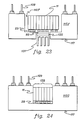
- Fig. 12 shows an hermetically sealed electronic package. Included in the package is electronic module 11 which may be formed using the techniques previously described herein. The electronic module is then bonded to interposer 95, which may be formed, using conventional substrate fabrication techniques, of a material such as a ceramic. The interposer provides a variety of functions for the electronic package. First, electrically conductive vias 85 formed within the interposer connect the electronic module to an active circuit layer, such as logic/control chip 93.
- an active circuit layer such as logic/control chip 93.
- the wiring within the interposer may be designed to facilitate the connection of "off-the-shelf" chips (such as a processor chip) with a predetermined contact pattern to an electronic module. Further, wiring 97 is provided within the interposer to connect the electronic package to external circuitry through electrical contacts 89 and leadframe connections 87. Optionally, the interposer may contain wiring (not shown) used to interconnect the various chips within the electronic module.
- a hermetically sealed package is necessary in certain environmentally stressful environments.
- a "thick" interposer such as a ceramic substrate, enables the electronic package to be hermetically sealed.
- Hermeticity is achieved across the interposer using hermetic caps 83 and 91 in conjunction with hermetic seals 99.
- a portion of the package may be hermetically sealed by only encapsulating one element of the package such as the stack of chips (11).
- non-hermetic sealing using, for example, a polymeric seal 99, e.g. a high temperature epoxy may be used to protect the package from an external environment.
- thin-film wiring/interconnect layer 101 is formed between the interposer and logic/control chip 103. Fabrication of layer 101 may be performed using the temporary workpiece techniques described herein. Layer 101 can be formed on a substrate, a flex or on a semiconductor chip. Functions provided by the thin-film wiring/interconnection layer include redistributing and busing signals between the electronic module and the logic/control chip, and providing for simplified interconnection between the logic/control chip and external circuitry. Layer 101 allows "off-the-shelf" processor or logic control chips to be used in conjunction with an electronic module. Layer 101 assures that proper pads of chip 103 are connected to pads of the electronic module. If chip 103 is large enough, layer 101 can be included as an additional wiring level on chip 103 itself. Thus, the standard off-the-shelf microprocessor can be converted by layer 101 to interface with pads of an electronic module.
- the additional layer of wiring/interconnection enables the use of a smaller logic/control chip because interconnection functions required of the logic/control chip have been simplified. As shown, in this embodiment, the physical area of the logic/control chip is smaller than the electronic module's side surface.
- hermetic sealing it is important that the thin-film wiring/interconnection layer (101) be contained within the hermetic cap area, because hermeticity can not be achieved across the polymeric passivation associated with a thin-film layer.
- the thin-film wiring/interconnect layer and logic/control chip are both contained within the area of hermetic cap 91. Hermeticity may thus be achieved on both sides of interposer substrate 95, protecting the electronic module and logic/control chip. It should also be noted that the portion of the interposer that extends beyond the hermetic cap is unsealed.
- non-hermetic sealing using, for example, a polymeric seal 99 may be used to protect the package from an external environment.
- FIGs. 14-15 Further embodiments of hermetically (or non-hermetically) sealed electronic packages are shown in Figs. 14-15 . Each of these embodiments includes alternate means for connecting the electronic package to external circuitry.
- two- sided leadframe 105 is used for connecting to external circuitry.
- another embodiment includes I/O pads 107 and adjoining I/O pins 109 used to connect to external circuitry. Accordingly, simple, standard connectivity to external circuits is provided.
- an electronic package may comprise a stack of memory chips. Associated therewith may be a logic/control chip, processor chip, or any active integrated circuit chip related to the function of the package.
- the memory may be primarily fast cache memory. Compared with current methods of packaging processors and associated cache memories, this invention provides significant advantages, including:
- the present invention provides several packaging embodiments to remove that heat notwithstanding the closely integrated electronic module.
- the invention also provides several embodiments for interconnecting the processor, the electronic module, the package and an external circuit board. Embodiments of such electronic packages are described in detail with respect to Figs. 16-26 below.
- Fig. 16 illustrates a processor/fast cache package.
- Processor chip 113 is die bonded to substrate 115A for thermal management and mechanical support. Electrical connectivity between the processor and the substrate (115A) is provided by wirebonds (111) connecting the processor to substrate wirebond pads 123. Within the substrate, signals are interconnected and then routed externally through input/output (I/O) pins 109.
- Processor chip 113 is also electrically connected to electronic module 11 by solder bump (29) bonding. Signals entering the electronic package at I/O pins 109 pass through conductive wiring (not shown) contained within substrate 115A and wirebonds 111 to processor chip 113 and electronic module 110.
- top surface 117 of cavity substrate 115A covers and protects the interior components.
- Heat can be removed from the package by, for example, the inherent heat radiating ability of substrate 115A, or the addition of cooling fins (not shown) on top surface (117) of substrate 115A.
- the packaging scheme provides the ability to remove heat from the processor despite the closely integrated electronic module.
- Logic/control chip 93 (one possible use being memory management) is bonded to cavity substrate 115B that removes heat and provides mechanical support. Wirebonds 111 electrically attach logic control chip 93 to substrate wirebond pads 123. Electronic module 11 is bonded to the logic/control chip on an end surface using die attach material 119. Additional wirebonds 111 electrically connect pads on the opposite end surface of the electronic module to both the logic/control chip and the substrate (115B). Wiring within substrate 115B interconnects I/O pins 109, electronic module 11, and logic/control chip 93 to form an integrated memory controller/memory package.
- wirebond pads 123 are located in various positions within the substrate's cavity to facilitate simplified wirebonding between structures. For example, first wirebond pad level 112 is closest to the logic/control chip and second wirebond pad level 114 is closest to the electronic module. Wirebonds are routed along the most efficient path between a structure and a corresponding wirebond pad level.
- lid 121 may be attached, covering the cavity and protecting the elements within.
- a thermally conductive compound (see, for example, Fig. 23) may be used to join the lid and the electronic module.
- the lid may be used to hermetically or non-hermetically seal the electronic package.
- a further enhancement entails the attachment of cooling fins (see, for example, Fig. 23) on the top-side of the substrate, resulting in a further improvement to the thermal management of the electronic module.
- Fig. 18 represents an embodiment of the present invention in which solder bump connections are used throughout.
- An end surface of a "pancake" format electronic module 11 is flush mounted within cavity 110C of cavity substrate 115C, and the resulting planar surface is solder bump bonded to processor chip 113.
- electronic module 11 is solder bump bonded to chip 113 and then chip 113 is solder bump bonded to the substrate 115C with electronic module 11 within cavity 110C.
- the substrate contains internal wiring (not shown) that connects the processor to the solder bump connections on the bottom surface of the substrate for connection to external circuitry. Heat is removed through a top lid thermally joined to chip 113 by thermal grease or thermal bonding.
- Yet another embodiment of the present invention is illustrated in Figs. 19-20 .
- both dynamic random access memory (DRAM) chips 125 and static random access memory (SRAM) chips 127 are contained within electronic module 11 ( Fig. 20 ).
- the processor chip is flush mounted within the cavity substrate (115D) so that the SRAM chips may, for example, act as a fast cache, and be solder bump (129) bonded directly to processor 113, while the DRAM chips may, for example, act as main memory, and be solder bump (131) bonded to the substrate (Note: Although solder bump connections 129 and 131 would not be visible in a top view, they are shown in the top schematic view of Fig. 20 for clarity).
- the processor chip and the substrate are electrically connected by wirebonds 111 leading from the processor to wirebond pads 123.
- this embodiment incorporates both a processor and multiple memory levels into a single, ultra-high density electronic package.
- wirebond interconnections between the electronic module, logic/control chip, and/or substrate wiring nets enable a cost effective technique to tailor the function of the electronic package to individual customer specifications.
- Multiple wirebond pads and wirebond interconnection patterns, i.e., "wirebond programming", between the electronic module, logic/control chip, and substrate can be used to vary the function of the electronic package. This wirebond programming provides substantial flexibility in the assembly of the package in that it can be done either prior to or subsequent to the mechanical coupling of the electronic module, logic/control chip, and substrate.
- a logic/control chip attached to an electronic module may provide a variety of memory management functions and capabilities. These may include, as previously discussed, for example, error correction, memory handshaking, automatic chip sparing within the stack, and/or buffering (see copending application Serial No. 08/220,086, entitled “Semiconductor Stack Structures and Fabrication/Sparing Methods Utilizing Programmable Spare Circuit.”). Examples of such arrangements are shown in Figs. 21-23 .
- Fig. 21 illustrates an embodiment of the present invention wherein logic/control chip 93 is flush mounted within cavity 110E of cavity substrate 115E. This enables electronic module 11 to be simultaneously solder bump bonded (29) to both the logic/control chip and the substrate.
- a thin-film wiring/interconnect layer (not shown) is optionally deposited between electronic module 11 and both logic/control chip 93 and substrate 115E. This layer provides electrical interconnection between the electronic module, active integrated circuit chip and substrate. In forming such a layer, the temporary workpiece techniques previously described herein, or conventional side-face metallization methods may be employed.
- flush mounted semiconductor structures e.g., chips and/or electronic modules
- bonded to various other semiconductor structures are possible.
- the embodiment of Fig. 22 includes cavity substrate 115F having both cavity 110F and opening 133.
- This opening enables (1) enhanced thermal management; (2) a wider range of electronic module build options; and (3) independent subcomponent removal and replacement.
- Thermal management is controlling the temperature of the device. It may include providing or removing heat.
- Shown in Fig. 23 is one such technology.
- Heat sink 137 is attached to the back side of logic control chip 93 using thermal compound 135 (such as thermal grease).
- the opening also permits various alternative build options to be exercised. For example, a variety of user selectable logic/control chips, or other types of chips (e.g., processor), may be selectively attached to a standard electronic module.
- a thin-film wiring/interconnect layer (not shown) may be used to interconnect substrate 115F, electronic module 11 and logic/control chip 93.
- Cooling channel 139 is fabricated in the substrate, providing for a direct gas or fluid coolant flow pathway around the electronic module. Supplemental thermal management may be provided by adding additional coolant flow channels in the substrate and/or attachment of heat transfer fins to the electronic module.
- FIG. 26 An hermetically sealed embodiment of the present invention incorporating a heat sink is shown in Fig. 26 .
- Hermetic seals 99 are disposed between heat sink 143 and cavity substrate 115H, and between hermetic cap 83 and substrate 115.
- Thermal management of the electronic module is provided by heat sink 143 attached to logic control chip 93 (by thermal compound 141), as well as heat transfer through hermetic cap 83.
- cooling fins could be attached to the hermetic cap or a thermal compound could be applied between the electronic module and the hermetic cap (neither shown).
- the hermetic seal may be replaced with a non-hermetic seal utilizing, for example, a high temperature epoxy.
- L1 cache memory, L2 cache memory and main (“L3") memory may be selectively disposed within an electronic module (or multiple electronic modules) electrically and mechanically coupled to the processor chip.
- Other chips associated with the processor may be added to the combination of processor and electronic memory module(s) providing further functions (for example, bus controllers, interface chips, or graphics controllers). Accordingly, a complete "computer unit" is formed in one package. Embodiments of such computer units are described in detail with respect to Figs. 27-32 below.
- Fig. 27 illustrates a computer unit containing multiple levels of cache memory and a main memory.
- Processor 150A contains cache memory controller 152 and L1 cache memory (not shown).
- the cache controller manages both L1 (on-chip) and L2 (off-chip) cache memory.
- the L2 cache memory is provided by electronic module 154, which includes a plurality of memory chips. Interconnection between the electronic module and the processor is provided by solder bumps (29).
- a second electronic module (156) including main memory chips (for example, DRAMs) is electrically and mechanically coupled to electronic module 154 by solder bumps.
- the solder bumps (29) electrically and mechanically bond to contacts disposed on a substantially planar surface of each electronic module. Formation of these electrical contacts may be performed using standard techniques for forming T-connects or through deposition of BLM pads as described herein.
- An interposer substrate (158) is electrically and mechanically bonded (using solder bumps) to a top surface of main memory electronic module 156. Further, main memory controller chip 160 is solder bump bonded to the top surface of interposer 158.
- Bussing chips 162 are disposed within both electronic modules. These chips provide a direct electrical connection from processor 150A through both sets of electronic modules up to, and through, interposer substrate 158 to memory controller 160. The memory controller then electrically communicates with the chips comprising main memory module 156 through electrical interconnections provided in interposer substrate 158.
- the resulting computer unit therefore includes: a processor chip having an integral L1 cache memory and L1/L2 cache memory controller; an L2 cache memory provided on an electronic module; a main memory provided on another electronic module; a main memory controller chip; and a combination of bussing chips and an interposer substrate closely interconnecting and integrating the entire computer unit.
- solder bump connections between the two electronic modules merely provide mechanical support.
- the only solder bumps disposed therein which provide electrical contact are those attached to busing chips 162.
- processor 150B has been provided without an on-chip L1 cache memory. Accordingly, electronic module 166 has been provided containing both L1 and L2 cache memories. It should be noted that this may comprise separate L1 and L2 cache memory circuits or one memory which serves as a very large L1 cache memory eliminating the need for L2 cache. This is possible because of the close integration of memory module 166 to processor chip 150B.
- High density Input/Output (“I/O") interconnect 164 is provided interconnecting the L1/L2 electronic module with the processor chip. (See, for example, U.S. Patent No. 5,202,754, "Three-Dimensional Multi Chip Packages and Method of Fabrication," issued April 13, 1993 and previously incorporated herein by reference).
- Integral L1/L2 cache memory 166 is controlled by cache memory controller 152 provided on the processor chip.
- Fig. 28 The remainder of the computer unit shown in Fig. 28 is similar to that shown in Fig. 27 . Specifically, an L3 main memory module (156) is provided, and solder bump bonded to integral L1/L2 cache memory module 166. Further, both interposer substrate 158 and main memory chip controller 160 have been provided, connected to the processor by busing chips 162 disposed within both electronic modules.
- the embodiment of the present invention shown in Fig. 29 represents a computer unit containing single electronic module 157 having three levels (L1, L2 and L3) of memory.
- main memory chips 156 for example, DRAMs
- Cache memory chips 166 for example, high speed SRAMs
- bussing chips 162 are disposed in the center of the stack of chips comprising electronic module 157.
- interposer substrate 158 and memory control chip 160 are included within the computer unit.
- I/O interconnect 164 Interconnection between processor 150C and combined L1/L2 memory is provided by high Input/Output ("I/O") interconnect 164. As shown, no direct connections exist between the main memory chips (156) and processor chip 150C. The computer unit is organized in this manner because all connections to main memory chips 156 take place through high I/O interconnect 164, bussing chips 162, main memory controller 160 and interposer substrate 158.
- Fig. 30 represents an enhancement to the computer unit of Fig. 29 , however, the additional features shown may be incorporated into the other embodiments described herein.
- Peripheral Component Interconnect (“PCI") bus controller 172 has been mechanically and electrically coupled to the interposer substrate 158 using solder bump bonding. Wiring within the interposer substrate connects PCI bus controller 172 to appropriate elements such as processor 150D and the memory chips of electronic module 159.
- bussing chip 170 has been added to the electronic module to connect PCI bus controller 172 (connected through interposer substrate 158) to processor chip 150D.
- the high I/O interconnect (164) has been extended to accommodate processor connections to busing chip 170.
- An interface cable (180) is mechanically and electrically connected to the interposer substrate (158).
- This cable provides electrical connection from PCI bus controller 172 to a PCI bus (not shown, external to the computer unit).
- the interposer substrate provides appropriate connections between the PCI bus controller and the interface cable.
- other types of interface chips could be used.
- a graphics controller could be substituted for the PCI bus controller integrating a graphics function within the computer unit.
- the interface cable would then provide external connection to the graphics controller.
- the graphics controller and the PCI bus controller could both be attached to the interposer substrate providing even more functions within the computer unit.
- any integrated circuit chip, or combination of integrated circuit chips, useful in conjunction with a computer unit may be implemented using the structures and methods described herein.
- Second interface cable 182 is shown attached to an end surface of electronic module 11.
- the second interface cable may electrically attach directly to one of the chips within the electronic module, or to an end or side surface metallization pattern (not shown).
- Metallization may be deposited using traditional techniques or those described herein.
- Second interface cable 182 may provide additional I/O functions for the computer unit, or may serve as an additional source of power and grounding. This may be necessary, to alleviate the need to distribute large amounts of power through the processor chip to the various componentry attached thereto. By supplying the power directly to the electronic module, processor chip 150D can have reduced wiring, and requires less heat dissipation.
- bussing chips are depicted in Figs. 31A-C . Regardless of the particular type of bussing chip, the bussing chips are located within electronic modules such that edge surfaces are parallel with side surfaces of the electronic module. Wiring 176 on bussing chip 162 electrically connects points on a first side surface of the electronic module to points on a second side surface of the electronic module.
- Fig. 31A shows bussing chip 162 containing wiring 176 that connects to two opposite edges of the chip.
- This type of chip is useful in the embodiments of the present invention depicted up to this point.
- wiring 176 need not be straight. Thus, wiring may connect to points not disposed opposite each other.
- Fig. 31B depicts a more complicated combination of wiring disposed on bussing chip 162A.
- Both "horizontal” and “vertical” wiring is shown connecting opposite edges of bussing chip 162.
- “arc” shaped bussing is shown connecting points on perpendicular edges of the bussing chip.
- the various wirings are located on different levels so as to be electrically insulated from each other. For example, most simply, all “horizontal” wirings are on one level, all “vertical” wirings are on another level and all “arc” wirings are on a third level. Alternatively, by using vias, all three wirings can be accommodated and kept insulated on two wiring levels.
- Bussing chip 178 of Fig. 31C represents an alternate technique for providing bussing from one surface of an electronic module to another surface.
- a typical IC chip with transfer wiring 175 is shown.
- additional "vertical" transfer wirings 176 are included within the transfer wiring layer to provide bussing connections.
- a single chip can provide both active functions and bus interconnects between surfaces of an electronic module containing the chip.
- the dedicated bussing chips of previous embodiments can be replaced with active chips having bussing wiring.
- an electronic module (188) is bonded to two processors (150E).
- the electronic module comprises all three levels (L1/L2 cache and L3 main) of memory.
- This memory is interconnected to the processors by means of high I/O interconnects (164).
- the combination of processors and electronic module is solder bump bonded to substrate 190. Wiring within the substrate facilitates interconnection of the various chips within the electronic module as well as external electrical contact through, for example, pins (not shown).
- each processor may have its own dedicated memory chips within the electronic module, or the processors may share common memory (of all levels). Coordination of activities between processors may be achieved through connections provided on bussing chips or through bussing contained on the individual integrated circuit chips within the stack (for example, as shown in Fig. 31C ), or either bussing method used in conjunction with wiring in the substrate.
Abstract
A fabrication method and resultant monolithic electronic module having a separately formed thin-film layer attached to a side surface. The fabrication method includes providing an electronic module (154,156) composed of stacked integrated circuit chips. A thin-film layer is separately formed on a temporary support which is used to attach the thin-film layer to the electronic module. The disclosed techniques may also be used for attaching an interposer (158), which may include active circuity, to an electronic module. Specific details of the fabrication method, resulting multichip packages, and various thin-film structures are set forth.
Description
- The present invention relates in general to high density electronic packaging which permits optimization of the number of circuit elements to be included in a given volume. More particularly, this invention relates to a technique for establishing a side surface interconnection structure on an electronic module, comprising for example a densely stacked array of multiple semiconductor layers interconnected at least partially by the interconnection structure. A variety of packaging options for electronic modules and associated elements are also presented. These include, for example, combinations of electronic modules and active integrated circuit chips coupled to various substrates. For example, this invention includes attaching an electronic module comprising memory chips to a processor chip. Further, encapsulated electronic packages are disclosed.
- Since the development of integrated circuit technology, computers and computer storage devices have been made from integrated circuit chips formed from wafers of semiconductor material. After a wafer is made, the chips are typically separated from each other by dicing the wafer. Thereafter, the individual chips are bonded to carriers of various types, interconnected by wires and packaged. As technology enhancements increase, more circuits are required per chip. This is accomplished by (a) making the circuits smaller and (b) making the chips larger. However, there is a practical limit to both. Making chips larger requires larger field size optics, which is now at a physical limitation. Thus, increasing the density by expanding the "two-dimensions" of the chips becomes prohibitive. Currently, physical chip size limitations are overcome by making chips as large as possible, and dividing the required entire circuit function into several chips, which are electrically connected together. However, this introduces undesirable signal delays, capacitance, and inductance, as signals travel between chips.
- Recently, semiconductor structures comprising three-dimensional arrays of chips have emerged as an important packaging approach. A typical three-dimensional electronic module (one example of a semiconductor structure) consists of multiple integrated circuit chips adhesively secured together as a monolithic structure (a "stack"). A metallization pattern is often provided directly on one (or more) side surface(s) of the electronic module for interconnecting the chips in the stack and for electrical connection of the stack to circuitry external to the module. The metallization pattern can include both individual contacts and bussed contacts, and multi-level wiring.
- One significant parameter in the fabrication of any electronic module is inter-chip spacing. If not controlled, then the number of semiconductor chips stackable in a given volume is potentially adversely affected because the wiring on the side of the stack takes into account the chip to chip final thickness. If the final thickness is allowed to vary too much, the wiring density on the side of the stack suffers. Also, the thickness of the individual semiconductor chips to be packaged in an electronic module can vary. The combined variance of the chip thickness and inter-chip spacing in turn causes alignment problems when a metallization pattern is to be formed directly on a side surface of the electronic module, as has been the conventional approach. This is because a prefabricated pattern mask is typically employed during the side surface metallization formation process and if inter-chip spacing is inconsistent, then alignment of the mask with the transfer wirings may be impossible.
- A number of methods have been proposed for regulating inter-chip spacing, including: selecting and ordering the chips so that the average spacing remains constant; varying the thickness of the adhesive layer to compensate for variances in inter-chip thicknesses (see, for example, U.S. Patent No. 4,999,311); or improving the consistency of the thickness of the chips and the adhesive layers. All of these methods are useful in forming the electronic module of the present invention.
- Typically, the metallization pattern is formed using photolithography directly on a side surface of the electronic module. Thus, conventional fabrication of the electronic module must be completed before side surface metallization begins. The extra process steps associated with lithography on a side surface detracts from the yield of functional electronic modules and can increase cost and complexity of electronic module fabrication. The fabrication technique proposed herein eliminates this complex sequential processing.
- Before an electronic module with associated side surface metallization may be incorporated into the next level of packaging, possibly interconnecting other chips, the electronic module must be appropriately packaged. In packaging electronic modules and related components, consideration must be given to the tradeoff between achieving high circuit density and providing means to remove heat.
- For example, it is desirable to locate a stack of memory chips (i.e., a memory module) in close proximity to other high-power electronic modules or high powered devices (such as processors). Close proximity, however, introduces a substantial heat dissipation problem. The present invention is also directed towards solving these problems.
- Briefly described, the present invention comprises, in a first aspect, a process for establishing a thin-film layer on a substantially planar surface of a semiconductor structure. The thin-film layer is first formed in association with a temporary support separate from the semiconductor structure. Thereafter, the layer is electrically coupled to the substantially planar surface of the semiconductor structure such that the thin-film layer physically bonds to the substantially planar surface, and the temporary support is coupled to the semiconductor structure. The temporary support is then decoupled from the semiconductor structure such that the thin-film layer remains electrically coupled and physically bonded to the substantially planar surface.
- As one enhancement, the thin-film layer may comprise a metallization layer and the semiconductor structure may comprise a plurality of stacked integrated circuit (IC) chips having a plurality of edge surfaces that at least partially define the substantially planar surface of the semiconductor structure. The electrical coupling step would then include electrically coupling the metallization layer to the substantially planar surface of the semiconductor structure such that the metallization layer at least partially electrically interconnects the stack of IC chips.
- In another aspect, the thin-film layer may comprise a metallization layer formed on a first main surface of a substrate; the substrate having an active circuit layer formed on a second main surface. The metallization layer and the active circuit layer are electrically connected by conductive vias, or trenches, in the substrate extending between the two main surfaces. Further, the active circuit layer may have electrical contacts disposed on it for facilitating electrical connection of the semiconductor structure to external circuitry.
- In an alternate aspect, the thin-film layer may comprise a first metallization layer formed on a first main surface of a passive film; the passive film having a second metallization layer formed on a second main surface. The metallization layers are connected by conductive vias in the passive film extending between the two main surfaces. Further, the second metallization layer may have electrical contacts disposed on it for facilitating electrical connection of the semiconductor structure to external circuitry.
- In both the passive film and substrate embodiments, processing might include, for example, formation of the various layers separate from the semiconductor structure on a temporary adhesive layer positioned on a temporary support. Processing then continues as described above. Specifically, the metallization layer is electrically coupled to the substantially planar surface of the semiconductor structure such that the metallization layer physically bonds thereto and the temporary support is physically coupled to the semiconductor structure. Thereafter, the temporary support is detached from the semiconductor structure along the temporary adhesive layer, while the metallization layer, substrate and active circuit layer (or second metallization layer) remain physically bonded to the substantially planar surface of the semiconductor structure.
- In yet another aspect, the present invention comprises a novel temporary workpiece for attaching a thin-film layer to a substantially planar surface of a semiconductor structure. The temporary workpiece includes a temporary support, a temporary adhesive layer disposed on a surface of the temporary support, and the thin-film layer coupled to the temporary support by the temporary adhesive layer. The workpiece may be employed to "transfer" the thin-film layer to the substantially planar surface of the semiconductor structure as summarized above. In particular, the thin-film layer can be physically bonded to the substantially planar surface of the semiconductor structure, after which the temporary support would be decoupled from the thin-film layer along with the temporary adhesive layer. The thin-film layer electrically connects to the semiconductor structure. As an enhancement, the workpiece may also include either an active circuit layer or a metallization layer for transfer with the thin-film layer to the semiconductor structure.
- In another aspect, the present invention consists of an enhanced electronic module comprising a semiconductor structure having a substantially planar surface, and a separately formed, thin-film layer bonded to the substantially planar surface of the semiconductor structure. The thin-film layer is electrically attached to the semiconductor structure, and provides functions associated therewith. By way of example, the thin-film layer may comprise a metallization layer. Alternatively, the thin-film layer may comprise an active circuit layer, in which case it provides functions associated with the semiconductor structure.
- If the thin-film layer is a first metallization layer, it may be formed on either a substrate or a passive film. The passive film might have a second metallization pattern formed on an opposite planar surface from the first metallization pattern; a substrate may have an active circuit layer formed on the opposite planar surface. In either case, the two opposite planar layers (e.g., first metallization layer and second metallization layer, or metallization layer and active circuit layer) may be electrically connected by conductive vias (or trenches) extending through the passive film or substrate. Further, either the active circuit layer or second metallization layer may have electrical contacts disposed on it for facilitating electrical connection of the electronic module to external circuitry.
- To restate, in all embodiments discussed up to this point, the present invention advantageously produces a semiconductor structure, for example, an electronic module comprising multiple IC chips, having separately formed side surface metallization. The metallization layer is transferred to the electronic module from a temporary support that is detached along a temporary adhesive layer. If desired, the metallization layer may be formed in conjunction with an active circuit layer and/or electrical contact pads for connecting the associated electronic module to an external device(s). Those skilled in the art will note that the metallization layer is established on the side surface of the electronic module without any lithography steps directly on the side surface of the module, thus avoiding the time, expense, inability to test or rework and complexity associated with complex processing on the side surface of the electronic module.
- The present invention further encompasses various packages for semiconductor structures, electronic modules and associated components as well as processes for creating the packages. In one embodiment, an electronic package includes an electronic module and an interposer having an active circuit layer for providing functions associated with the electronic module. The electronic module comprises a stack of integrated circuit chips whose edges partially define a side surface of the module. The substrate has a substantially planar main surface which is electrically and mechanically coupled to the side surface of the electronic module. As an enhancement, the side surface of the electronic module may have a length x and the substantially planar surface of the substrate may have a length y, wherein x ≤ y. Further, the electronic package may include a cap which may hermetically seal the electronic module.
- In another aspect, the present invention comprises an electronic package having an electronic module, a cavity substrate having a cavity therein, and an active integrated circuit chip. The electronic module comprises a stack of integrated circuit chips and has a substantially planar surface. The active integrated circuit chip is mechanically coupled to, and disposed between, the substantially planar surface of the electronic module and the cavity substrate. Both the electronic module and the active integrated circuit chip are recessed within the substrate's cavity. As an enhancement, the cavity substrate may be formed to have a plurality of wirebond pad levels for efficiently accommodating wirebond connections to structures contained within the electronic package.
- A further aspect of the invention includes an electronic package comprising a cavity substrate having a cavity therein, a first semiconductor structure, and a second semiconductor structure. The first semiconductor structure is contained within the cavity such that the substrate and a substantially planar surface of the first element comprise a substantially planar receiving surface. Mechanically coupled to this surface is the second semiconductor structure. As an enhancement, the first semiconductor structure may be an active integrated circuit chip and the second semiconductor structure may be an electronic module comprising a stack of integrated circuit chips. Alternatively, the elements corresponding to the first and second semiconductor structures may be interchanged.
- In yet another aspect, the present invention encompasses an electronic package comprising an electronic module having a stack of integrated circuit chips, and a substrate having both a cavity and an opening therein. Recessed within the cavity is the electronic module having a substantially planar surface mechanically coupled to the substrate. As an enhancement, the opening may facilitate a coolant to pass around the electronic module for cooling the module. Further, the opening may accommodate an active integrated circuit chip attached to the electronic module, and even a means for thermal management attached to the active integrated circuit chip.
- A further aspect of the present invention comprises a computer unit having a processor chip and a first electronic module, and method for forming the same. The processor chip has a substantially planar main surface and includes a cache memory controller. The first electronic module comprises a plurality of stacked integrated circuit chips and has a first substantially planar surface. Further, the first electronic module includes a cache memory circuit. The substantially planar main surface of the processor chip is mechanically and electrically coupled to the first substantially planar surface of the first electronic module such that the cache memory controller is electrically connected to the cache memory circuit.
- As an enhancement, the first electronic module may have a second substantially planar surface having a first plurality of electrical contacts thereon. At least some of the electrical contacts are electrically coupled to the processor chip for facilitating electrical contact to the processor. Furthermore, the invention may comprise a second electronic module having a plurality of stacked IC chips and having a first substantially planar surface. The second electronic module also includes a second memory circuit. The first substantially planar surface of the second electronic module is mechanically coupled to the second substantially planar surface of the first electronic module such that the first and second electronic modules are electrically coupled via the first plurality of electrical contacts on the first electronic module.
- The subject matter which is regarded as the present invention is particularly pointed out and distinctly claimed in the concluding portion of the specification. The invention, however, both as to organization and method of practice, together with further objects and advantages thereof, may best be understood by reference to the following detailed description taken in conjunction with the accompanying drawings in which:
- Fig. 1 is a partial cross-sectional view of a stack of multiple semiconductor chips laminated together according to an embodiment of the present invention;
- Fig. 2A is a partial cross-sectional view of the stack of Fig. 1 subsequent to partial removal of a side surface of the stack;
- Fig. 2B is a partial cross-sectional view of the stack of Fig. 2A subsequent to the patterned formation of an insulating layer on the planarized side surface;
- Fig. 3A is a partial cross-sectional view of the stack of Fig. 2A subsequent to the preferential removal of a portion of the edges of the chips pursuant to the present invention;
- Fig. 3B is a partial cross-sectional view of the stack of Fig. 3A subsequent to the formation of an insulating layer on the edges of the chips and exposing of the interchip transfer metal leads;
- Fig. 4 is a perspective view of an electronic module and Molybdenum (Mo) mask according to the present invention;
- Fig. 5 is a partial cross-sectional view of an electronic module after completion of fabrication in accordance with one embodiment of the present invention;
- Fig. 5A is a partial cross-sectional view of the electronic module of Fig. 5 subsequent to the removal of a solder bump;
- Fig. 5B is a partial cross-sectional view of a fabricated electronic module having an insulated electrical contact pursuant to an embodiment of the present invention;
- Fig. 5C is a partial cross-sectional view of a fabricated electronic module having a multi-size/multi-layer contact with one contact surface electrically insulated;
- Fig. 6 is a partial cross-sectional view of an electronic module having a thin-film structure (including a metallization layer), and a temporary support coupled thereto in accordance with the present invention;
- Fig. 7 is a partial cross-sectional view of the electronic module of Fig. 6 after the temporary support has been removed;
- Fig. 8 is a partial cross-sectional view of an alternate embodiment of the electronic module of Fig. 7, wherein balancing pads are interposed between the thin-film structure and the semiconductor chips;
- Fig. 9 is a partial cross-sectional view of an electronic module having a passive film (including two metallization layers), and a temporary support coupled thereto in accordance with the present invention;
- Fig. 10 is a partial cross-sectional view of the electronic module of Fig. 9 after the temporary support has been removed;
- Fig. 11 is a perspective view of an electronic module having thinned layers bonded to two side surfaces thereof in accordance with the present invention;
- Fig. 12 is a cross-sectional view of a hermetically sealed electronic package containing an electronic module and an associated logic/control chip;
- Fig. 13 is a cross-sectional view of the hermetically sealed electronic package of Fig. 12 having a thin-film metallization layer disposed between the interposer and the logic/control chip;
- Fig. 14 is a cross-sectional view of the hermetically sealed electronic package of Fig. 12 with external electrical connection provided by a two-sided leadframe;
- Fig. 15 is a cross-sectional view of the hermetically sealed electronic package of Fig. 12 with external electrical connection provided by input/output pins;
- Fig. 16 is a cross-sectional view of an electronic package having an electronic module in a "loaf" format bonded to a processor, both contained within a cavity substrate;
- Fig. 17 is a cross-sectional view of an electronic package having an electronic module fabricated in a "pancake" format bonded to a logic/control chip, both wirebonded to various wirebond pad levels with a cavity substrate;
- Fig. 18 is a cross-sectional view of an electronic package having a "pancake" format electronic module recessed flush within a substrate, with a processor chip being solder bump bonded to both the substrate and the electronic module;
- Figs. 19 and 20 are cross-sectional and top-schematic views, respectively, of an electronic package wherein an electronic module is bonded by solder bumps to both a flush mounted processor chip and a substrate;
- Fig. 21 is a cross-sectional view of an electronic package having an electronic module bonded to both a substrate and a flush mounted logic/control chip;
- Fig. 22 is a cross-sectional view of a three-dimensional electronic package wherein an electronic module is bonded to both a substrate and a logic/control chip which is contained within an opening in the substrate;
- Fig. 23 is a cross-sectional view of the electronic package of Fig. 22 having a heat sink added to the logic control chip for enhanced thermal management of the package;
- Figs. 24 and 25 are side and top views, respectively, of an electronic package having cooling channels provided within the substrate to enhance thermal management of the package;
- Fig. 26 is a cross-sectional view of a hermetically sealed electronic package with enhanced thermal management;
- Fig. 27 is a cross-sectional view of a computer unit with multiple memory levels contained in multiple electronic modules in accordance with the present invention;
- Fig. 28 is a cross-sectional view of the computer unit of Fig. 27 having a high I/O interconnect electrically coupling the processor to an electronic module;
- Fig. 29 is a cross-sectional view of a computer unit of the present invention having three levels of memory contained in a single electronic module;
- Fig. 30 is a cross-sectional view of the computer unit of Fig. 29 having a PCI bus controller chip as well as an interface cable for connection of the computer unit to the PCI bus;
- Figs. 31A·C are schematic views of busing chips in accordance with the present invention; and
- Fig. 32 is a cross-sectional view of a computer unit having multiple processors sharing a common electronic module containing three levels of memory.
- Certain preferred embodiments for establishing a metallization layer on a side surface of a semiconductor structure are presented herein. While particular embodiments presented describe a semiconductor structure comprising an electronic module, other semiconductor structures may be utilized (for example, wafers or IC chips).
- Fig. 1 is a partial cross-sectional view of an
electronic module 11, comprising a plurality of stacked integrated circuit chips 13 (a plurality of chips, "stacked" to form an electronic module). Typical functions implemented bychips 13 may include, for example, memory, interface, processor (for example, a microprocessor) and/or control functions, although each chip may include any function known in the art for implementation on a semiconductor chip. Atransfer metal 15 is associated with each integrated circuit (IC) chip to connect the IC chip to other chips inelectronic module 11 or to external circuitry. When stacked,transfer metal 15 ofchips 13 extend towards at least one selectedside surface 14 of the unprocessedelectronic module 11.Insulator 17, disposed on the surface of eachchip 13 both above and belowtransfer metal 15, electrically insulates and physically isolates the respective transfer metal(s). The semiconductor chips are laminated together via layers of an adhesive 19. - As a specific example,
electronic module 11 may comprise a memory module, with eachsemiconductor chip 13 having arespective insulator layer 17, such as a polyimide, formed above the active surface of the chip.Insulator 17 also electrically insulates the respective transfer metal(s) 15, which may comprise a Ti/Al(Cu) structure.Transfer metal 15 electrically connects to the active I/O pads of the respective chips via conventional metallized vias formed in theinsulator 17. The layers of adhesive may comprise any one of various commercially available high-temperature adhesive materials, such as Thermid manufactured by National Starch and Chemical Co., Bridgewater, N.J. - As a specific process example, once the semiconductor chips have been laminated into a stack, the selected
side surface 14 undergoes processing to expose the ends of the transfer metal 15 (Fig. 2A). Thereafter, aninsulation layer 21 is deposited and patterned so as to formvias 22 to the exposed ends of transfer metal 15 (Fig. 2b). Thus, transfermetal 15 extends to the chip edges with adequate insulation but without the need for alternate insulating means (for example, a moat of insulation formed underneath the transfer metal). - An alternative example of insulating the selected side surface of the electronic module and exposing the ends of the transfer metal is depicted in Figs. 3A & 3B. Once the semiconductor chips have been laminated into a stack, selected
side surface 14 undergoes processing to expose the transfer metal 15 (Fig. 2A). The edges ofchips 13 are preferentially removed (Fig. 3A), e.g., using a selective etch process. Thereafter, an insulation layer is deposited and planarized, e.g. polishing, to expose only the ends of the transfer metal 15 (Fig. 3B). - As shown in Figs. 4 & 5, appropriate
electrical contacts 27 are next formed on theresultant side surface 25 ofelectronic module 11 in association with therespective transfer metal 15. Formation of these electrical contacts may proceed by use of a Molybdenum (Mo) mask 20 (Fig. 4) havingholes 22 formed therein located to align with the exposedtransfer metal 15 when the mask is appropriately positioned on the side surface of the electronic module. - It should be noted that the T-Connect structure depicted in Fig. 5 (and subsequent figures) have been simplified for reasons of clarity. T-Connects are typically formed by well known processes including the deposition of a metallurgical structure on the side surface of electronic modules such as, for example, those shown in Fig. 2B or Fig. 3B.
- As shown in Fig. 5, in one embodiment, Ball Limiting Metallurgy (BLM)
pads 27 are used as electrical contacts. Formation of BLMs can be accomplished through the masking/evaporation process described above. In particular, a BLM structure can be created by evaporating a three layer metal structure composed of chrome, copper and gold. Alternately, structures of, for example, Ni/Au, Ti/Cu/Au, Cu, Cr/Cu and Ti/Cu may be used. Onceelectrical contacts 27 have been deposited on the electronic module, solder bumps 29 may be formed on the electrical contacts using thesame Mo mask 20. Afterbumps 29 have been formed, the electronic module is ready for soldering to external electrical circuitry (not shown) or chip interconnect metallization (described below). - Note that the process described herein above for forming BLM pads with solder bumps is achieved without any photolithography (or other lithography) steps. The process is faster, easier, and less expensive than photolithography processes used to achieve a functionally similar structure (such as fabricating T-connect pads on a surface of an electronic module using photolithography steps).
- A variation of this process that is capable of handling shorts (or other severe electrical defects) associated with specific chips in the stack entails: (1) deposition of the BLM pads and solder bumps on the side surface of the electronic module; (2) electrical test of the chips comprising the electronic module; and (3) electrical isolation of the defective chip(s) by removal of the solder bumps (Fig. 5A) associated with the BLM pads connected to the defective chip(s). When the electronic module is joined to the next level of assembly (e.g., a substrate/temporary workpiece) there will be no mechanical or electrical interconnection between the BLM pads and the substrate/temporary workpiece pads on which the solder bumps have been removed. This technique is a particularly good processing option in that no photolithographic steps are required.
- A further process that is capable of handling shorts (or other severe electrical defects) associated with specific chips in the stack entails: (1) deposition of the BLM pads on the side surface of the electronic module; (2) electrical test of the chips comprising the electronic module; (3) electrical isolation of defective chip(s) (accomplished by depositing an insulation layer over the BLM pads connected to the defective chips); and (4) redeposition of BLM pad and solder bumps. As described above, the BLM and solder bump deposition may utilize a Mo mask process. The deposition of an insulation layer, for example, polyimide, would entail application, patterning, and curing techniques that are well known and currently practiced in the microelectronics industry. Moreover, the redepositions of a BLM pad ensures that solder bumps over the electrically isolated chips adhere well to the surface and act as mechanical support solder bumps when joined to the next level of assembly.
- Fig. 5B illustrates the resulting structure following this process wherein
electrical insulation layer 27A is used to isolatechip 13A to which transfer metal 15A is connected. Theinsulation layer 27A thickness is chosen (for example, 1- 3µm) such that the height variation between electrically connected and non-connected solder bumps is not significant and can easily be accommodated in the join to the next level of assembly. - Variations on this process, exploiting the same inventive concepts are also possible. An alternative process entails executing this selective isolation process on the substrate contact pads to which the electronic module will be joined.
- Moreover, a further variation used to electrically isolate the defective chip(s) is shown in Fig. 5C. Although similar to Fig. 5B regarding the use of an insulating layer (27A) to isolate a defective chip, the contact pads are sized significantly differently. Bottom contact pad 27' is sized larger than the
BLM 27 disposed above it. This difference in size is useful with respect to the testing of the chips within the module. Particularly, before the BLM pads (27) are deposited, probes are used which make contact with contact pads 27'. These probes may cause damage to the surface of the contact pads. Thus, by provisioning the pads larger than the BLMs deposited on top of them, testing is performed to areas of the bottom contact pads at locations outside where the BLMs will be deposited. Thus, the areas on which the BLMs are deposited are undisturbed by the test probes. In order to eliminate solder wetting pad 27' during solder reflow, a non-wettable material such as, for example, chrome can be used as the top layer of pad 27'. - An additional benefit regarding the larger bottom contact pads is derived with respect to the inter-chip spacing tolerance of the electronic module. If the chip lamination processes result in a large variation in the inter chip spacing, then larger contact pads will be required in order to "capture," i.e., electrically contact, all of the transfer metal leads 15 presented to the side surface of the module. The smaller BLM pads may then be deposited on top of the larger pads, without regard to variances in inter-chip spacing.
- If a contact needs to be electrically isolated (i.e., a defective chip) an insulating layer may be used similar to the embodiment shown in Fig. 5B. Again, an insulating layer (Fig. 5C, 27A) is deposited between the contact pad and the BLM pad disposed above it. In this particular embodiment, the insulation layer must be larger than in previous embodiments (Fig. 5B) in order to account for the larger sized bottom contact pad.
- Fig. 6 depicts one embodiment of a separate side surface interconnect/active circuit structure, generally denoted
thin film structure 41, pursuant to the present invention. A temporary support 57 (composed of, for example, silicon) provides a physically strong temporary support forstructure 41, which resides thereon during fabrication and attachment of the structure to the electronic module. Advantageously, supportingstructure 57 enables the fabrication and attachment of layers to the electronic module that likestructure 41 are significantly thinner and mechanically weaker than conventional semiconductor structures. Thus, "thin-film" structures, such as thin-film structure 41, can be attached to the electronic module without fabricating them directly on the electronic module. - A thin-film structure such as thin-
film structure 41 may be fabricated using standard wafer processing techniques. To begin, a wafer comprising IC chips having deep conductive trenches (i.e., vias) is fabricated (see, for example, U.S. Patent No. 5,202,754, "Three-Dimensional Multi Chip Packages and Method of Fabrication," issued April 13, 1993 and incorporated herein by reference). The wafer is then mounted onto a temporary workpiece using a temporary adhesive (the active side of the wafer faces the temporary workpiece). The mounted wafer is then thinned using mechanical and/or chemical techniques, exposing the conductive trenches. Thin-film layers are then built on the wafer, connected to the exposed conductive trenches. These layers may be composed of appropriate combinations of metallization and insulation. The wafer/temporary workpiece combination is then diced forming "thinned two-sided chips" attached to a temporary workpiece. - The temporary workpiece is necessary during this fabrication for providing mechanical support. For example, high yield deposition of insulating films on thin wafers would not be possible without the temporary workpiece. The wafers are far too fragile to withstand the forces developed during, for example, "spin apply" of insulation.
- In accordance with the present invention,
temporary support 57 is removed oncestructure 41 has been electrically and mechanically connected to the electronic module via solder bumps 29. This is made possible by interposing temporaryadhesive layer 59 betweenstructure 41 andtemporary support 57. Many temporary adhesives for use in semiconductor fabrication processing are known in the art, one example being Ditac, manufactured by E.I. DuPont De Nemours and Co. Another temporary adhesive is Ultem, manufactured by General Electric Corp. The combination oftemporary support 57, adhesive 59 andstructure 41 comprises a "temporary workpiece" that transfersstructure 41 to the electronic module. This is because when the temporary support is removed, thin-film structure 41 remains physically and electrically attached to the electronic module via the solder bumps. - Fig. 7 shows the resultant electronic module after
temporary support 57 has been removed along the temporary adhesive layer.Layer 51 ofstructure 41 comprises a metallization layer, which has been formed on asubstrate 49. This metallization layer serves two functions. First, as described below, contacts are provided to match those of the electronic module. Second, metallization 51 interconnects at least some of themultiple chips 13 within the electronic module (i.e., at least some chips are electrically connected to at least some other chips).Metallization layer 51 can comprise any standard wiring/metallization layout previously directly formed on the side surface of the electronic module. -
Electrical contacts 53 are formed onmetallization layer 51 to facilitate electrical attachment of the metallization layer toBLM pads 27 via the solder bumps 29.Electrical contacts 53 may be formed by well known masking/evaporation techniques, for example, by evaporation of BLM pads. Note that solder bumps 29 formed onBLM pads 27 may alternately be formed onelectrical contacts 53 of thin-film structure 41, or on a combination of bothpads 27 andcontacts 53. Whichever embodiment, solder will be reflowed onto both sets of electrical contacts (or BLM pads) to provide a proper electrical/mechanical connection ofstructure 41 to the side surface of the electronic module. - Specifically, attachment can be achieved by physically positioning the electronic module so that the
BLM pads 27 are aligned with theelectrical contacts 53. Once properly positioned, heat is applied until solder bumps 29 melt. The solder bumps are then allowed to cool, thereby establishing a good mechanical and electrical connection. A polymeric material 55 (for example, a silica or alumina filled high-temperature epoxy) is preferably added between thin-film structure 41 and the electronic module to enhance the mechanical connection. - Continuing with the description of the thin-film structure, an
active circuit layer 45 is disposed on a planar surface ofsubstrate 49 opposite frommetallization layer 51.Active circuit layer 45 may implement any one of various functions, again depending upon thechips 13 to which the layer is connected. For example, ifchips 13 comprise memory chips, then theactive circuit layer 45 might, for instance, provide a memory controller function. - In one embodiment,
substrate 49 is formed using the thin-film techniques described in commonly assigned U.S. Patent No. 5,270,261, entitled: "Three Dimensional Multichip Package Methods of Fabrication," issued December 14, 1993 and incorporated herein by reference. Briefly summarized, this patent teaches the formation of a stacked chip structure including "trench" interconnects running through a thinned substrate. Using this technique, electrically conductive trenches 47 (i.e., vias) can be formed throughsubstrate 49 so as to extend between its two main planar surfaces, and if desired, to electricallyinterconnect metallization layer 51 andactive circuit layer 45.Trenches 47 significantly simplify electrical connection between layers ofstructure 41, reduce the need for external interconnect wiring, and further increase interconnect density of the resultant electronic module. - It is also possible that thin-
film structure 41 will be flipped over, using a second temporary adhesive and a second temporary support, so that the active circuit layer will be connected adjacent to the electronic module. This provides an advantage in terms of signal propagation. - To continue in the current embodiment, provision is made for connection of thin-
film structure 41, and the electronic module to which it is affixed, to external circuitry. In this regard,electrical contacts 43 are deposited on an exposed surface ofactive circuit layer 45 ofstructure 41.Contacts 43 can be deposited beforeactive circuit layer 45 is adhesively attached totemporary support 57.Contacts 43 can also be deposited after thin-film structure 41 has been transferred to the electronic module. Conventional techniques may be used to deposit these electrical contacts.Contacts 43 may electrically connect to respective semiconductor chips in the electronic module, toactive circuit layer 45, or to both. Many different methods are known in the art which can be used for connecting toelectrical contacts 43, including, for example, solder bumps, Tape Automated Bonding (TAB) or wirebond technologies. - From the above discussion, those skilled in the art will note that a highly sophisticated, electronic module has been presented with side surface interconnects, active control circuitry, and contacts ready for electrical attachment to external devices. However, note that the presented structure comprises only one embodiment of the inventive concepts set forth herein. By way of example, variations on the basic inventive concepts are next presented.
- As one variation, the process step of laminating semiconductor chips together into an electronic module (a "stack" of integrated circuit chips) may be eliminated if used in combination with a thin-film structure such as presented above. In such an embodiment, spacers could be employed between the semiconductor chips in place of the permanent adhesive layers 19. As shown in Fig. 8,
spacers 65 can provide uniform chip spacing within the electronic module and protect the active surface of each semiconductor chip during fabrication processing. Preferably, uniform interchip spacing is maintained within the electronic module by selecting the widths ofindividual spacers 65 to compensate for variation in the widths of the semiconductor chips comprising the electronic module.Spacers 65 provide greater control over inter-chip spacing than the use of an adhesive layer between chips, thereby reducing alignment problems with masks, and allowing stacks of greater numbers of chips to be fabricated. Further, if desired, the spacers can be removed after the electronic module is bonded to the metallization layer in order to facilitate improved thermal management (e.g. dissipation of heat from the electronic module by allowing air or liquid to flow between the chips). - The methods used to form
electrical contacts 27 on an unglued stack of semiconductor chips differ from the methods presented above. This is because an unglued stack of chips must be aligned and then the alignment must be maintained whileelectrical contacts 27 on the thin-filmed structure are formed, e.g., using the techniques discussed above. One approach to maintaining alignment of the stack is to use a spring-loaded fixture (not shown). - After
chips 13, separated byspacers 65, have been soldered to a thin-film structure (such asstructure 41 of Fig. 7), additional mechanical support for the chips might be needed. This is because the stack is not held together by adhesive, and individual chips are mechanically supported only by, e.g., the BLM pads on the edges of the chips. Thus, the chips may tend to tilt, placing mechanical stress on the electrical contacts on both the electronic module and the thin-film structures. - As shown in Fig. 8, 'balancing'
pads 63, fabricated on the edge of each chip, can be used to mechanically supportchips 13 on thin-film structure 41. These provide support so that eachchip 13 may rest on its edge without placing undue stress on associated "active"BLM pads 27. Balancingpads 63 can be fabricated using a Mo mask, with holes corresponding to desired balancing pad locations, in conjunction with conventional evaporation techniques. Both "active" and "balancing" pads may be formed simultaneously by using a Mo mask containing both sets of mask holes. The thickness of balancingpads 63 will then be such as to properly support the associated chips. - As another variation, the thin-film structure may comprise a passive film. Referring to Figs. 9-10, passive film 71 (one type, for example, is known as a 'flex circuit'), is electrically and mechanically bonded to the electronic module. In the particular embodiment shown in Figs. 9 and 10, the electronic module has a preexisting side
surface metallization layer 79, which may be formed by conventional techniques known in the art (optionally,layer 79 may be omitted). Similar to thin-film structure 41 (Figs. 6-8), the passive film contains afirst metallization layer 73 disposed on a main planar surface bonded to the electronic module. The opposite planar surface of the passive film contains asecond metallization layer 75, rather than theactive circuit layer 45 of Figs. 6-8. However, the remaining structure associated with the passive film is similar to that of the thin-film structure of the embodiment presented above. Electrical contacts are disposed on both surfaces of the passive film for connecting the first metallization layer to the electronic module, and the second metallization layer to external circuitry, respectively. Electricallyconductive vias 77 interconnect both metallization layers, thereby allowing signals to pass between the electronic module (connected to the first metallization layer) to external circuitry (connected to the second metallization layer). - Numerous materials exist for forming a passive film including polyimide tape for the flex circuit and a wide range of ceramic substrates. In a manner similar to the formation of the previously described thin-film structure, a passive film can be built in layers on a temporary workpiece 57 (Fig. 9.). The workpiece is used during fabrication of the passive film, and subsequent bonding of the electronic module. In this particular embodiment, however, fabrication does not begin with a base chip. Instead, thin-film layers of metallization and insulation are built up on top of the temporary support/temporary adhesive layer. Vias are opened up within the layers as appropriate, interconnecting various thin-film layers within the film. After bonding has taken place, the temporary workpiece is removed along temporary adhesive 59 (Figs. 10), with the passive film remaining bonded to the electronic module.
- The passive film can have many functions associated therewith. For example, it may be used to (a) provide electrical "bus" connections between chips of the electronic module; (b) provide electrical replacement of a defective chip(s) in the electronic module with spare chips in the module; and (c) provide complex interconnection of the chips within the electronic module in association with the signals provided by external circuitry.
- In accordance with the present invention, use of a passive film containing metallized interconnects offers many advantages over conventional side surface metallization. The passive film (1) may be fabricated separate from the electronic module; (2) may contain personalized metallization patterns on both surfaces of the film; and (3) is less expensive than conventional side surface metallization. Personalization processes known in the art for passive film fabrication include (a) line removal processes (for example, laser ablation); (b) line add processes (for example, laser chemical vapor deposition or staple bonding); and (c) prefabrication of the film.
- As yet another embodiment, shown in Fig. 11, an active circuit layer 81 (for example, processor circuitry) may be formed on a second side surface of the electronic module. This embodiment thus utilizes side surface processing (for example, deposition of BLM pads) on two side surfaces of the stack, which may be performed as previously described herein for one side surface. Thin-film structure 41 (or passive film 71) is bonded to a first side surface, while an
active circuit layer 81 is formed and deposited on a second side surface using the temporary workpiece and thin-film techniques described above, or using standard processor chips that have been thinned. - Advantageously, by providing an active circuit layer on a second side surface of the electronic module, the first surface
active circuit layer 45 and associated electrically conductive trenches 47 (Fig. 7) may no longer be necessary (however, the transfer metallurgy pattern on each chip of the electronic module becomes more complex because it must connect to two edges (comprising the two side surfaces), as well as the I/O pads on the surface of each chip). Thus, an electronic module with a thin-film structure bonded to a first side surface, and an active circuit layer bonded to a second side surface is formed. Furthermore, these techniques may be extended to provide various combinations of thin or conventional structures on more than two side surfaces of the electronic module. An electronic module with an attached structure such as separately formed side-surface metallization, is considered an "enhanced" electronic module. - As a further variation of the present invention, the electrical contacts on the electronic module may be formed by a plurality of different processes. Such processes are known in the art, and can be accomplished without lithography steps, thus eliminating the time, complexity, and expense associated therewith. For example, an electroplating process may be used to deposit BLM pads. Alternatively, an electroless plating process may be used. Specifically, the stack of chips could be dipped into a sequence of tanks, each to deposit a respective metal. The metals deposit preferentially on exposed conductors, so alignment of the
transfer metals 15 with electrical contacts would be automatic. There is a limitation to this process, however. Transfer metal conductors are typically only 1-3 µm wide, so the electroless plating BLM pads would be very narrow. - As another variation, the electrical contacts on the electronic module may be electrically and mechanically attached to contacts on the thin-film structures, substrates or other electronic modules using techniques other than soldering. Alternative techniques would include, for example, the use of conductive polymers, polymer-metal composite pastes or anisotropic conductive polymers.
- Further, depending on the electronic module, the function of
active circuit layer 45 may vary. As one embodiment, chips 13 might comprise memory chips, in which case the circuitry may act as a memory buffer and a memory control overseeing memory allocation and utilization. Moreover, this function may be especially important should aspecific chip 13 fail and need to be replaced, or spared, with anotherchip 13 in the electronic module 11 (see copending applications Serial No. 08/120,876, entitled: "Integrated Multichip Memory Module, Structure and Fabrication," and Serial No. 08/120,993, entitled: "Integrated Memory Cube, Structure and Fabrication"). - Alternatively,
active circuit layer 45 may provide a means to replace failed bits within one or more semiconductor chips of the electronic module (see copending application Serial No. 08/220,086, entitled: "Semiconductor Stack Structures and Fabrication/Sparing Methods Utilizing Programmable Spare Circuit"). In another embodiment, the active circuitry may provide customer specific functions such as, for example, error correction, memory handshaking, or a self-test (see, for example, copending applications Serial No. 08/120,876, entitled: "Integrated Multichip Memory Module, Structure and Fabrication," and Serial No. 08/120,993, entitled: "Integrated Memory Cube, Structure and Fabrication"). Thus,active circuit layer 45 may provide a wide variety of functions in support of the stack of integrated circuit chips 13. - The concepts and techniques of the present invention may be used to fabricate a variety of high-density electronic packages. Advantageously, as is known, higher density packaging results in shorter interconnections between components, yielding a higher speed, better performing electronic package.
- As one embodiment, Fig. 12 shows an hermetically sealed electronic package. Included in the package is
electronic module 11 which may be formed using the techniques previously described herein. The electronic module is then bonded tointerposer 95, which may be formed, using conventional substrate fabrication techniques, of a material such as a ceramic. The interposer provides a variety of functions for the electronic package. First, electricallyconductive vias 85 formed within the interposer connect the electronic module to an active circuit layer, such as logic/control chip 93. - The wiring within the interposer may be designed to facilitate the connection of "off-the-shelf" chips (such as a processor chip) with a predetermined contact pattern to an electronic module. Further, wiring 97 is provided within the interposer to connect the electronic package to external circuitry through
electrical contacts 89 andleadframe connections 87. Optionally, the interposer may contain wiring (not shown) used to interconnect the various chips within the electronic module. - A hermetically sealed package is necessary in certain environmentally stressful environments. The use of a "thick" interposer, such as a ceramic substrate, enables the electronic package to be hermetically sealed. Hermeticity is achieved across the interposer using
hermetic caps hermetic seals 99. A portion of the package may be hermetically sealed by only encapsulating one element of the package such as the stack of chips (11). Optionally, non-hermetic sealing using, for example, apolymeric seal 99, e.g. a high temperature epoxy may be used to protect the package from an external environment. - Another embodiment of a hermetically sealed electronic package is shown in Fig. 13. In addition to the structures previously recited, thin-film wiring/
interconnect layer 101 is formed between the interposer and logic/control chip 103. Fabrication oflayer 101 may be performed using the temporary workpiece techniques described herein.Layer 101 can be formed on a substrate, a flex or on a semiconductor chip. Functions provided by the thin-film wiring/interconnection layer include redistributing and busing signals between the electronic module and the logic/control chip, and providing for simplified interconnection between the logic/control chip and external circuitry.Layer 101 allows "off-the-shelf" processor or logic control chips to be used in conjunction with an electronic module.Layer 101 assures that proper pads ofchip 103 are connected to pads of the electronic module. Ifchip 103 is large enough,layer 101 can be included as an additional wiring level onchip 103 itself. Thus, the standard off-the-shelf microprocessor can be converted bylayer 101 to interface with pads of an electronic module. - The additional layer of wiring/interconnection enables the use of a smaller logic/control chip because interconnection functions required of the logic/control chip have been simplified. As shown, in this embodiment, the physical area of the logic/control chip is smaller than the electronic module's side surface.
- When hermetic sealing is used, it is important that the thin-film wiring/interconnection layer (101) be contained within the hermetic cap area, because hermeticity can not be achieved across the polymeric passivation associated with a thin-film layer. As shown, the thin-film wiring/interconnect layer and logic/control chip are both contained within the area of
hermetic cap 91. Hermeticity may thus be achieved on both sides ofinterposer substrate 95, protecting the electronic module and logic/control chip. It should also be noted that the portion of the interposer that extends beyond the hermetic cap is unsealed. Optionally, non-hermetic sealing using, for example, apolymeric seal 99 may be used to protect the package from an external environment. - Further embodiments of hermetically (or non-hermetically) sealed electronic packages are shown in Figs. 14-15. Each of these embodiments includes alternate means for connecting the electronic package to external circuitry. In the embodiment shown in Fig. 14, two-
sided leadframe 105 is used for connecting to external circuitry. As shown in Fig. 15, another embodiment includes I/O pads 107 and adjoining I/O pins 109 used to connect to external circuitry. Accordingly, simple, standard connectivity to external circuits is provided. - Other embodiments of high-density electronic packages are possible. For example, an electronic package may comprise a stack of memory chips. Associated therewith may be a logic/control chip, processor chip, or any active integrated circuit chip related to the function of the package. As one example, the memory may be primarily fast cache memory. Compared with current methods of packaging processors and associated cache memories, this invention provides significant advantages, including:
- 1. The ultra high density capability of the electronic package technology described herein allows much larger cache memories to be provided.
- 2. There is a significant performance advantage due not only to the higher density of the electronic module, but also due to the intimate interconnection between the electronic module and the processor. There are no intervening levels of packaging with all their associated delays and system performance impacts.
- 3. Because the cache memory is now in intimate contact with the processor, one can now envision a migration of level one ("L1") cache memory from the processor chip to the closely spaced memory chips of the electronic module. This simplifies the design and fabrication of the processor chip by substantially reducing its size and cost. Note: L1 cache memory is typically the fastest cache memory and is usually located on the processor chip.
- 4. This simplified processor chip coupled with its reduced size can now be fabricated at much higher yields per wafer.
- 5. An alternative for the standard processor having on-chip L1 cache and having a larger and slower level two ("L2") cache externally on separate modules is a processor and an electronic module directly connected together, the electronic module having both L1 and L2 memory in one package. The integration of L1 and L2 caches is made possible by the reduced wiring delay, improved access time, higher hit ratio, and larger size of the memory in the closely coupled electronic module.
- 6. Main memory, which is even larger and slower than L2 cache, may also be incorporated into an electronic module coupled to a processor chip. Again, the tight integration of memory and processor increases speed, and overall density of the system.
- 7. All of these advantages cumulatively translate directly into lower product cost and higher system performance, thereby enabling higher profit margins compared with the current methods for providing this function to the end user.
- High speed processors generate a lot of heat that must be removed. The present invention provides several packaging embodiments to remove that heat notwithstanding the closely integrated electronic module. The invention also provides several embodiments for interconnecting the processor, the electronic module, the package and an external circuit board. Embodiments of such electronic packages are described in detail with respect to Figs. 16-26 below.
- As one embodiment, Fig. 16 illustrates a processor/fast cache package.
Processor chip 113 is die bonded to substrate 115A for thermal management and mechanical support. Electrical connectivity between the processor and the substrate (115A) is provided by wirebonds (111) connecting the processor tosubstrate wirebond pads 123. Within the substrate, signals are interconnected and then routed externally through input/output (I/O) pins 109.Processor chip 113 is also electrically connected toelectronic module 11 by solder bump (29) bonding. Signals entering the electronic package at I/O pins 109 pass through conductive wiring (not shown) contained within substrate 115A and wirebonds 111 toprocessor chip 113 andelectronic module 110. - Structurally,
electronic module 11 andprocessor 113 are completely recessed within cavity 110A in cavity substrate 115A. When mounted to, for example, a printed circuit board,top surface 117 of cavity substrate 115A covers and protects the interior components. Heat can be removed from the package by, for example, the inherent heat radiating ability of substrate 115A, or the addition of cooling fins (not shown) on top surface (117) of substrate 115A. The packaging scheme provides the ability to remove heat from the processor despite the closely integrated electronic module. - Another electronic package is shown in Fig. 17. Logic/control chip 93 (one possible use being memory management) is bonded to cavity substrate 115B that removes heat and provides mechanical support.
Wirebonds 111 electrically attachlogic control chip 93 tosubstrate wirebond pads 123.Electronic module 11 is bonded to the logic/control chip on an end surface using die attachmaterial 119.Additional wirebonds 111 electrically connect pads on the opposite end surface of the electronic module to both the logic/control chip and the substrate (115B). Wiring within substrate 115B interconnects I/O pins 109,electronic module 11, and logic/control chip 93 to form an integrated memory controller/memory package. - A unique organization of wirebonds interconnect
electronic module 11, logic/control chip 93 and substrate 115B, all being contained withincavity 110B of cavity substrate 115B. As shown,wirebond pads 123 are located in various positions within the substrate's cavity to facilitate simplified wirebonding between structures. For example, firstwirebond pad level 112 is closest to the logic/control chip and secondwirebond pad level 114 is closest to the electronic module. Wirebonds are routed along the most efficient path between a structure and a corresponding wirebond pad level. - After fabrication is complete,
lid 121 may be attached, covering the cavity and protecting the elements within. As an enhancement, a thermally conductive compound (see, for example, Fig. 23) may be used to join the lid and the electronic module. In addition, the lid may be used to hermetically or non-hermetically seal the electronic package. A further enhancement entails the attachment of cooling fins (see, for example, Fig. 23) on the top-side of the substrate, resulting in a further improvement to the thermal management of the electronic module. - Fig. 18 represents an embodiment of the present invention in which solder bump connections are used throughout. An end surface of a "pancake" format
electronic module 11 is flush mounted within cavity 110C ofcavity substrate 115C, and the resulting planar surface is solder bump bonded toprocessor chip 113. Alternatively,electronic module 11 is solder bump bonded tochip 113 and then chip 113 is solder bump bonded to thesubstrate 115C withelectronic module 11 within cavity 110C. The substrate contains internal wiring (not shown) that connects the processor to the solder bump connections on the bottom surface of the substrate for connection to external circuitry. Heat is removed through a top lid thermally joined to chip 113 by thermal grease or thermal bonding. Yet another embodiment of the present invention is illustrated in Figs. 19-20. In this embodiment, both dynamic random access memory (DRAM)chips 125 and static random access memory (SRAM)chips 127 are contained within electronic module 11 (Fig. 20). The processor chip is flush mounted within the cavity substrate (115D) so that the SRAM chips may, for example, act as a fast cache, and be solder bump (129) bonded directly toprocessor 113, while the DRAM chips may, for example, act as main memory, and be solder bump (131) bonded to the substrate (Note: Althoughsolder bump connections wirebond pads 123. Advantageously, this embodiment incorporates both a processor and multiple memory levels into a single, ultra-high density electronic package. - The wirebond interconnections between the electronic module, logic/control chip, and/or substrate wiring nets enable a cost effective technique to tailor the function of the electronic package to individual customer specifications. Multiple wirebond pads and wirebond interconnection patterns, i.e., "wirebond programming", between the electronic module, logic/control chip, and substrate can be used to vary the function of the electronic package. This wirebond programming provides substantial flexibility in the assembly of the package in that it can be done either prior to or subsequent to the mechanical coupling of the electronic module, logic/control chip, and substrate.
- A logic/control chip attached to an electronic module may provide a variety of memory management functions and capabilities. These may include, as previously discussed, for example, error correction, memory handshaking, automatic chip sparing within the stack, and/or buffering (see copending application Serial No. 08/220,086, entitled "Semiconductor Stack Structures and Fabrication/Sparing Methods Utilizing Programmable Spare Circuit."). Examples of such arrangements are shown in Figs. 21-23.
- Fig. 21 illustrates an embodiment of the present invention wherein logic/
control chip 93 is flush mounted withincavity 110E of cavity substrate 115E. This enableselectronic module 11 to be simultaneously solder bump bonded (29) to both the logic/control chip and the substrate. A thin-film wiring/interconnect layer (not shown) is optionally deposited betweenelectronic module 11 and both logic/control chip 93 and substrate 115E. This layer provides electrical interconnection between the electronic module, active integrated circuit chip and substrate. In forming such a layer, the temporary workpiece techniques previously described herein, or conventional side-face metallization methods may be employed. - It should be generally noted that other combinations of flush mounted semiconductor structures (e.g., chips and/or electronic modules) bonded to various other semiconductor structures are possible.
- The embodiment of Fig. 22 includes cavity substrate 115F having both
cavity 110F andopening 133. This opening enables (1) enhanced thermal management; (2) a wider range of electronic module build options; and (3) independent subcomponent removal and replacement. In addition to the inherent heat transfer provided by the opening, it may be used to add low cost thermal management technologies. Thermal management is controlling the temperature of the device. It may include providing or removing heat. Shown in Fig. 23 is one such technology.Heat sink 137 is attached to the back side oflogic control chip 93 using thermal compound 135 (such as thermal grease). The opening also permits various alternative build options to be exercised. For example, a variety of user selectable logic/control chips, or other types of chips (e.g., processor), may be selectively attached to a standard electronic module. Further, the opening permits the logic/control chip to be removed for repair and/or replacement in a simplified manner. In a similar manner to the embodiment of Fig. 22, a thin-film wiring/interconnect layer (not shown) may be used to interconnect substrate 115F,electronic module 11 and logic/control chip 93. - Yet another embodiment incorporating advanced thermal management is shown in the two views presented in Figs. 24-25.
Cooling channel 139 is fabricated in the substrate, providing for a direct gas or fluid coolant flow pathway around the electronic module. Supplemental thermal management may be provided by adding additional coolant flow channels in the substrate and/or attachment of heat transfer fins to the electronic module. - An hermetically sealed embodiment of the present invention incorporating a heat sink is shown in Fig. 26.
Hermetic seals 99 are disposed betweenheat sink 143 andcavity substrate 115H, and betweenhermetic cap 83 andsubstrate 115. Thermal management of the electronic module is provided byheat sink 143 attached to logic control chip 93 (by thermal compound 141), as well as heat transfer throughhermetic cap 83. In a further embodiment, cooling fins could be attached to the hermetic cap or a thermal compound could be applied between the electronic module and the hermetic cap (neither shown). In yet another embodiment, if a hermetic seal is not required, and only mechanical protection for the components is, the hermetic seal may be replaced with a non-hermetic seal utilizing, for example, a high temperature epoxy. - The close integration of an electronic module(s) comprising memory chips with a processor chip permits a variety of different memory organizations and structures. Particularly, L1 cache memory, L2 cache memory and main ("L3") memory may be selectively disposed within an electronic module (or multiple electronic modules) electrically and mechanically coupled to the processor chip. Other chips associated with the processor may be added to the combination of processor and electronic memory module(s) providing further functions (for example, bus controllers, interface chips, or graphics controllers). Accordingly, a complete "computer unit" is formed in one package. Embodiments of such computer units are described in detail with respect to Figs. 27-32 below.
- As one embodiment, Fig. 27 illustrates a computer unit containing multiple levels of cache memory and a main memory.
Processor 150A containscache memory controller 152 and L1 cache memory (not shown). The cache controller manages both L1 (on-chip) and L2 (off-chip) cache memory. The L2 cache memory is provided byelectronic module 154, which includes a plurality of memory chips. Interconnection between the electronic module and the processor is provided by solder bumps (29). - A second electronic module (156) including main memory chips (for example, DRAMs) is electrically and mechanically coupled to
electronic module 154 by solder bumps. The solder bumps (29) electrically and mechanically bond to contacts disposed on a substantially planar surface of each electronic module. Formation of these electrical contacts may be performed using standard techniques for forming T-connects or through deposition of BLM pads as described herein. - An interposer substrate (158) is electrically and mechanically bonded (using solder bumps) to a top surface of main memory
electronic module 156. Further, mainmemory controller chip 160 is solder bump bonded to the top surface ofinterposer 158. - A novel method of electrical interconnection between the elements is provided within the computer unit shown in Fig. 27. Bussing
chips 162 are disposed within both electronic modules. These chips provide a direct electrical connection fromprocessor 150A through both sets of electronic modules up to, and through,interposer substrate 158 tomemory controller 160. The memory controller then electrically communicates with the chips comprisingmain memory module 156 through electrical interconnections provided ininterposer substrate 158. The resulting computer unit therefore includes: a processor chip having an integral L1 cache memory and L1/L2 cache memory controller; an L2 cache memory provided on an electronic module; a main memory provided on another electronic module; a main memory controller chip; and a combination of bussing chips and an interposer substrate closely interconnecting and integrating the entire computer unit. - It should be noted that the majority of solder bump connections between the two electronic modules merely provide mechanical support. The only solder bumps disposed therein which provide electrical contact are those attached to
busing chips 162. - In another embodiment shown in Fig. 28,
processor 150B has been provided without an on-chip L1 cache memory. Accordingly,electronic module 166 has been provided containing both L1 and L2 cache memories. It should be noted that this may comprise separate L1 and L2 cache memory circuits or one memory which serves as a very large L1 cache memory eliminating the need for L2 cache. This is possible because of the close integration ofmemory module 166 toprocessor chip 150B. - One of the advantages of on-chip cache memory is the large number of interconnections available between processor and memory, permitting wide words. The present invention provides comparable or greater total number of interconnections between the processor chip and the integrated L1/L2 cache memory module. High density Input/Output ("I/O")
interconnect 164 is provided interconnecting the L1/L2 electronic module with the processor chip. (See, for example, U.S. Patent No. 5,202,754, "Three-Dimensional Multi Chip Packages and Method of Fabrication," issued April 13, 1993 and previously incorporated herein by reference). Integral L1/L2 cache memory 166 is controlled bycache memory controller 152 provided on the processor chip. - The remainder of the computer unit shown in Fig. 28 is similar to that shown in Fig. 27. Specifically, an L3 main memory module (156) is provided, and solder bump bonded to integral L1/L2
cache memory module 166. Further, bothinterposer substrate 158 and mainmemory chip controller 160 have been provided, connected to the processor by busingchips 162 disposed within both electronic modules. - The embodiment of the present invention shown in Fig. 29 represents a computer unit containing single electronic module 157 having three levels (L1, L2 and L3) of memory. In particular, main memory chips 156 (for example, DRAMs) are grouped at "opposite" ends of the electronic module. Cache memory chips 166 (for example, high speed SRAMs) are grouped together "inside" the main memory chips. As in the previous embodiments, bussing
chips 162 are disposed in the center of the stack of chips comprising electronic module 157. Other organizations of various types of chips within the electronic module are also possible. Again, as in the previous embodiments,interposer substrate 158 andmemory control chip 160 are included within the computer unit. - Interconnection between
processor 150C and combined L1/L2 memory is provided by high Input/Output ("I/O")interconnect 164. As shown, no direct connections exist between the main memory chips (156) andprocessor chip 150C. The computer unit is organized in this manner because all connections tomain memory chips 156 take place through high I/O interconnect 164, bussingchips 162,main memory controller 160 andinterposer substrate 158. - Fig. 30 represents an enhancement to the computer unit of Fig. 29, however, the additional features shown may be incorporated into the other embodiments described herein. Peripheral Component Interconnect ("PCI")
bus controller 172 has been mechanically and electrically coupled to theinterposer substrate 158 using solder bump bonding. Wiring within the interposer substrate connectsPCI bus controller 172 to appropriate elements such asprocessor 150D and the memory chips of electronic module 159. For example, as shown, bussingchip 170 has been added to the electronic module to connect PCI bus controller 172 (connected through interposer substrate 158) toprocessor chip 150D. It will be noted, as shown, that the high I/O interconnect (164) has been extended to accommodate processor connections tobusing chip 170. - An interface cable (180) is mechanically and electrically connected to the interposer substrate (158). This cable provides electrical connection from
PCI bus controller 172 to a PCI bus (not shown, external to the computer unit). The interposer substrate provides appropriate connections between the PCI bus controller and the interface cable. Similarly, other types of interface chips could be used. For example, a graphics controller could be substituted for the PCI bus controller integrating a graphics function within the computer unit. The interface cable would then provide external connection to the graphics controller. Alternatively, the graphics controller and the PCI bus controller could both be attached to the interposer substrate providing even more functions within the computer unit. In fact, any integrated circuit chip, or combination of integrated circuit chips, useful in conjunction with a computer unit may be implemented using the structures and methods described herein. -
Second interface cable 182 is shown attached to an end surface ofelectronic module 11. The second interface cable may electrically attach directly to one of the chips within the electronic module, or to an end or side surface metallization pattern (not shown). Metallization may be deposited using traditional techniques or those described herein. -
Second interface cable 182 may provide additional I/O functions for the computer unit, or may serve as an additional source of power and grounding. This may be necessary, to alleviate the need to distribute large amounts of power through the processor chip to the various componentry attached thereto. By supplying the power directly to the electronic module,processor chip 150D can have reduced wiring, and requires less heat dissipation. - Various types of bussing chips are depicted in Figs. 31A-C. Regardless of the particular type of bussing chip, the bussing chips are located within electronic modules such that edge surfaces are parallel with side surfaces of the electronic module. Wiring 176 on bussing
chip 162 electrically connects points on a first side surface of the electronic module to points on a second side surface of the electronic module. - As a first example, Fig. 31A shows bussing
chip 162 containingwiring 176 that connects to two opposite edges of the chip. This type of chip is useful in the embodiments of the present invention depicted up to this point. As shown, wiring 176 need not be straight. Thus, wiring may connect to points not disposed opposite each other. - Fig. 31B depicts a more complicated combination of wiring disposed on bussing
chip 162A. Both "horizontal" and "vertical" wiring is shown connecting opposite edges of bussingchip 162. Further, "arc" shaped bussing is shown connecting points on perpendicular edges of the bussing chip. In this particular example, it should be noted that the various wirings are located on different levels so as to be electrically insulated from each other. For example, most simply, all "horizontal" wirings are on one level, all "vertical" wirings are on another level and all "arc" wirings are on a third level. Alternatively, by using vias, all three wirings can be accommodated and kept insulated on two wiring levels. - Bussing
chip 178 of Fig. 31C represents an alternate technique for providing bussing from one surface of an electronic module to another surface. A typical IC chip withtransfer wiring 175 is shown. However, additional "vertical" transfer wirings 176 are included within the transfer wiring layer to provide bussing connections. Thus, a single chip can provide both active functions and bus interconnects between surfaces of an electronic module containing the chip. Thus, the dedicated bussing chips of previous embodiments can be replaced with active chips having bussing wiring. - The techniques of the present invention may be applied to multiprocessor implementations of computer units. As shown in Fig. 32, an electronic module (188) is bonded to two processors (150E). The electronic module comprises all three levels (L1/L2 cache and L3 main) of memory. This memory is interconnected to the processors by means of high I/O interconnects (164). The combination of processors and electronic module is solder bump bonded to
substrate 190. Wiring within the substrate facilitates interconnection of the various chips within the electronic module as well as external electrical contact through, for example, pins (not shown). - The electrical connections from each processor to the substrate are achieved through
bussing chip 162A. Becausesubstrate 190 is perpendicular to each processor chip, "arc" type wiring as shown in Fig. 31B is used. As a general note, each processor may have its own dedicated memory chips within the electronic module, or the processors may share common memory (of all levels). Coordination of activities between processors may be achieved through connections provided on bussing chips or through bussing contained on the individual integrated circuit chips within the stack (for example, as shown in Fig. 31C), or either bussing method used in conjunction with wiring in the substrate. - While the invention has been described in detail herein in accordance with certain preferred embodiments thereof, many modifications and changes therein may be effected by those skilled in the art. Accordingly, it is intended by the appended claims to cover all such modifications and changes as fall within the true spirit and scope of the invention.
Claims (17)
- A method for forming a computer unit comprising the steps of:(a) providing a processor chip having a substantially planar main surface, said processor chip including a cache memory controller;(b) providing a first electronic module comprising a plurality of stacked integrated circuit (IC) chips and having a first substantially planar surface, said first electronic module including a cache memory circuit; and(c) mechanically and electrically coupling the first substantially planar surface of the first electronic module to the substantially planar surface of the processor chip such that the cache memory controller is electrically connected to the cache memory circuit.
- The method of claim 1, wherein said providing step (b) includes providing the first electronic module with a second substantially planar surface, said second substantially planar surface having a first plurality of electrical contacts thereon, at least some electricalcontacts of said first plurality of electrical contacts being electrically coupled to said processor chip for facilitating electrical contact to said processor chip.
- The method of claim 2, wherein said computer unit includes a second processor chip having a substantially planar main surface, and wherein said method includes mechanically and electrically coupling the substantially planar main surface of the second processor chip to the second substantially planar surface of the first electronic module.
- The method of claim 2 or 3, wherein the providing step (b) further comprises providing a bussing chip within the plurality of stacked IC chips of the first electronic module, said bussing chip having a first edge surface parallel with the first substantially planar surface of the first electronic module, and a second edge surface parallel with the second substantially planar surface of the first electronic module, and wherein said bussing chip electrically connects the processor chip coupled to the first substantially planar surface of the first electronic module to the at least some electrical contacts of the first plurality of electrical contacts coupled to the second substantially planar surface of the electronic module.
- The method of claim 2, 3 or 4, wherein the computer unit includes an interposer substrate having a substantially planar main surface, and wherein said method includes mechanically coupling the substantially planar main surface of the interposer substrate to the second substantially planar surface of the first electronic module such that said interposer substrate electrically attaches to the first plurality of electrical contacts and at least partially electrically interconnects the plurality of stacked IC chips of the first electronic module.
- The method of anyone of claims 2 to 5, wherein said computer unit includes a second electronic module comprising a plurality of stacked IC chips and having a first substantially planar surface, said second electronic module including a second memory circuit, and wherein said method further comprises mechanically coupling the first substantially planar surface of the second electronic module to the second substantially planar surface of the first electronic module such that the first electronic module and second electronic module are electrically coupled via the first plurality of electrical contacts such that the second electronic module is electrically coupled to the processor chip.
- The computer unit of claim 6, wherein the second electronic module has a second substantially planar surface, said second substantially planar surface having a second plurality of electrical contacts thereon, and wherein said step of mechanically coupling the first substantially planar surface of the second electronic module to the second substantially planar surface of the first electronic module includes electrically coupling at least some of said electrical contacts of said second plurality of electrical contacts through said at least some electrical contacts of said first electronic module to said processor chip, for providing electrical contact to devices associated with said computer unit.
- The computer unit of claim 7, wherein said computer unit includes a main memory controller chip having a substantially planar main surface, and wherein said method includes mechanically coupling the substantially planar main surface of the main memory controller chip to the second substantially planar surface of the second electronic module such that said main memory controller chip is electrically coupled to the at least some electrical contacts of the second plurality of electrical contacts of the second electronic module.
- The computer unit of claim 8, wherein the plurality of stacked IC chips of the second electronic module includes a bussing chip, said bussing chip having a first edge surface parallel with the first substantially planar surface of the second electronic module, and a second edge surface parallel with the second substantially planar surface of the second electronic module, and wherein said step of mechanically coupling the first substantially planar surface of the second electronic module to the second substantially planar surface of the first electronic module includes electrically connecting the at least some electrical contacts of the first plurality of electrical contacts of the first electronic module to the at least some electrical contacts of the second plurality of electrical contacts of the second electronic module using said bussing chip.
- The computer unit of anyone of claims 1 to 9, wherein said providing step (b) includes providing a first electronic module having a main memory circuit, said electrical coupling step (c) being such that the main memory circuit functions in association with the processor chip.
- A computer unit comprising means for implementing anyone of the method steps of claims 1 to 10.
- The computer unit of claim 11 further, including an interface chip having a substantially planar main surface mechanically and electrically coupled to the second substantially planar surface of the first electronic module such that said interface chip is electrically coupled to the at least some electrical contacts of the first plurality of electrical contacts electrically coupled to the processor chip.
- The computer unit of claim 11 or 12, wherein the plurality of stacked IC chips of the first electronic module includes an active integrated circuit chip, said active integrated circuit chip having a first edge surface parallel with the first substantially planar surface of the first electronic module, and a second edge surface parallel with the second substantially planar surface of the first electronic module, and wherein said active integrated circuit chip electrically connects the processor chip coupled to the first substantially planar surface of the first electronic module to the at least some electrical contacts of the first plurality of electrical contacts coupled to the second substantially planar surface of the electronic module.
- The computer unit of claim 11, 12 or 13, further including an interface cable electrically and mechanically connected to the interposer substrate for facilitating external electrical connection to the computer unit via the interposer substrate.
- The computer unit of anyone of claims 11 to 14, further comprising a high density interconnect disposed between and mechanically and electrically coupling the first electronic module to the processor chip.
- The computer unit of anyone of claims 11 to 15, wherein the first electronic module has a second substantially planar surface, and wherein the computer unit includes an interface cable mechanically and electrically coupled to said second substantially planar surface.
- The computer unit of anyone of claims 11 to 16, wherein the cache memory circuit comprises a combined level one ("L1") cache memory circuit and level two ("L2") cache memory circuit.
Applications Claiming Priority (2)
| Application Number | Priority Date | Filing Date | Title |
|---|---|---|---|
| US08/313,976 US5567654A (en) | 1994-09-28 | 1994-09-28 | Method and workpiece for connecting a thin layer to a monolithic electronic module's surface and associated module packaging |
| US313976 | 1994-09-28 |
Publications (1)
| Publication Number | Publication Date |
|---|---|
| EP0706220A1 true EP0706220A1 (en) | 1996-04-10 |
Family
ID=23218000
Family Applications (1)
| Application Number | Title | Priority Date | Filing Date |
|---|---|---|---|
| EP95480148A Withdrawn EP0706220A1 (en) | 1994-09-28 | 1995-09-22 | Method and workpiece for connecting a thin layer to a monolithic electronic module's surface and associated module packaging |
Country Status (3)
| Country | Link |
|---|---|
| US (3) | US5567654A (en) |
| EP (1) | EP0706220A1 (en) |
| TW (2) | TW377500B (en) |
Cited By (6)
| Publication number | Priority date | Publication date | Assignee | Title |
|---|---|---|---|---|
| DE19725464A1 (en) * | 1996-06-17 | 1997-12-18 | Lg Semicon Co Ltd | Semiconductor chip stack housing |
| EP0827203A2 (en) * | 1996-08-20 | 1998-03-04 | International Business Machines Corporation | Clock skew minimisation system and method for integrated circuits |
| WO1999019911A1 (en) * | 1997-10-10 | 1999-04-22 | Gennum Corporation | Three-dimensional packaging configuration for multi-chip module assembly |
| WO1999036962A1 (en) * | 1998-01-15 | 1999-07-22 | Infineon Technologies Ag | Semiconductor component with several substrate layers and at least one semiconductor chip and method for producing a semiconductor component |
| EP1598868A1 (en) * | 2004-05-18 | 2005-11-23 | Texas Instruments Inc. | Stacked dies having shared access to memory |
| CN105789139A (en) * | 2016-03-31 | 2016-07-20 | 上海新储集成电路有限公司 | Method for preparing neural network chip |
Families Citing this family (148)
| Publication number | Priority date | Publication date | Assignee | Title |
|---|---|---|---|---|
| US5946553A (en) * | 1991-06-04 | 1999-08-31 | Micron Technology, Inc. | Process for manufacturing a semiconductor package with bi-substrate die |
| US5567654A (en) * | 1994-09-28 | 1996-10-22 | International Business Machines Corporation | Method and workpiece for connecting a thin layer to a monolithic electronic module's surface and associated module packaging |
| KR0137826B1 (en) * | 1994-11-15 | 1998-04-28 | 문정환 | Package method and device package |
| US5657537A (en) * | 1995-05-30 | 1997-08-19 | General Electric Company | Method for fabricating a stack of two dimensional circuit modules |
| EP0774888B1 (en) | 1995-11-16 | 2003-03-19 | Matsushita Electric Industrial Co., Ltd | Printed wiring board and assembly of the same |
| US5952725A (en) | 1996-02-20 | 1999-09-14 | Micron Technology, Inc. | Stacked semiconductor devices |
| US5880530A (en) * | 1996-03-29 | 1999-03-09 | Intel Corporation | Multiregion solder interconnection structure |
| US5903045A (en) * | 1996-04-30 | 1999-05-11 | International Business Machines Corporation | Self-aligned connector for stacked chip module |
| FR2748851B1 (en) * | 1996-05-15 | 1998-08-07 | Commissariat Energie Atomique | PROCESS FOR PRODUCING A THIN FILM OF SEMICONDUCTOR MATERIAL |
| US6784023B2 (en) * | 1996-05-20 | 2004-08-31 | Micron Technology, Inc. | Method of fabrication of stacked semiconductor devices |
| JP2842378B2 (en) * | 1996-05-31 | 1999-01-06 | 日本電気株式会社 | High-density mounting structure for electronic circuit boards |
| DE19626126C2 (en) * | 1996-06-28 | 1998-04-16 | Fraunhofer Ges Forschung | Method for forming a spatial chip arrangement and spatial chip arrangement |
| US6043559A (en) * | 1996-09-09 | 2000-03-28 | Intel Corporation | Integrated circuit package which contains two in plane voltage busses and a wrap around conductive strip that connects a bond finger to one of the busses |
| US6498074B2 (en) | 1996-10-29 | 2002-12-24 | Tru-Si Technologies, Inc. | Thinning and dicing of semiconductor wafers using dry etch, and obtaining semiconductor chips with rounded bottom edges and corners |
| JP3537447B2 (en) * | 1996-10-29 | 2004-06-14 | トル‐シ・テクノロジーズ・インコーポレイテッド | Integrated circuit and manufacturing method thereof |
| US6882030B2 (en) | 1996-10-29 | 2005-04-19 | Tru-Si Technologies, Inc. | Integrated circuit structures with a conductor formed in a through hole in a semiconductor substrate and protruding from a surface of the substrate |
| JP2964983B2 (en) * | 1997-04-02 | 1999-10-18 | 日本電気株式会社 | Three-dimensional memory module and semiconductor device using the same |
| US6551857B2 (en) * | 1997-04-04 | 2003-04-22 | Elm Technology Corporation | Three dimensional structure integrated circuits |
| US5915167A (en) * | 1997-04-04 | 1999-06-22 | Elm Technology Corporation | Three dimensional structure memory |
| US5892287A (en) * | 1997-08-18 | 1999-04-06 | Texas Instruments | Semiconductor device including stacked chips having metal patterned on circuit surface and on edge side of chip |
| US6069026A (en) * | 1997-08-18 | 2000-05-30 | Texas Instruments Incorporated | Semiconductor device and method of fabrication |
| US6525414B2 (en) | 1997-09-16 | 2003-02-25 | Matsushita Electric Industrial Co., Ltd. | Semiconductor device including a wiring board and semiconductor elements mounted thereon |
| US7786562B2 (en) * | 1997-11-11 | 2010-08-31 | Volkan Ozguz | Stackable semiconductor chip layer comprising prefabricated trench interconnect vias |
| FR2773261B1 (en) | 1997-12-30 | 2000-01-28 | Commissariat Energie Atomique | METHOD FOR THE TRANSFER OF A THIN FILM COMPRISING A STEP OF CREATING INCLUSIONS |
| US6140696A (en) | 1998-01-27 | 2000-10-31 | Micron Technology, Inc. | Vertically mountable semiconductor device and methods |
| US6091138A (en) * | 1998-02-27 | 2000-07-18 | Advanced Micro Devices, Inc. | Multi-chip packaging using bump technology |
| US6137164A (en) * | 1998-03-16 | 2000-10-24 | Texas Instruments Incorporated | Thin stacked integrated circuit device |
| US6147411A (en) * | 1998-03-31 | 2000-11-14 | Micron Technology, Inc. | Vertical surface mount package utilizing a back-to-back semiconductor device module |
| US6104082A (en) * | 1998-04-24 | 2000-08-15 | International Business Machines Corporation | Metallization structure for altering connections |
| KR100290886B1 (en) * | 1998-05-09 | 2001-07-12 | 김영환 | ultra high density integrated circuit semiconductor package and method for fabricating the same |
| US6025638A (en) * | 1998-06-01 | 2000-02-15 | International Business Machines Corporation | Structure for precision multichip assembly |
| US6320126B1 (en) * | 1998-07-14 | 2001-11-20 | Texas Instruments Incorporated | Vertical ball grid array integrated circuit package |
| US6281042B1 (en) * | 1998-08-31 | 2001-08-28 | Micron Technology, Inc. | Structure and method for a high performance electronic packaging assembly |
| US6219237B1 (en) | 1998-08-31 | 2001-04-17 | Micron Technology, Inc. | Structure and method for an electronic assembly |
| US6586835B1 (en) * | 1998-08-31 | 2003-07-01 | Micron Technology, Inc. | Compact system module with built-in thermoelectric cooling |
| US6392296B1 (en) | 1998-08-31 | 2002-05-21 | Micron Technology, Inc. | Silicon interposer with optical connections |
| US6049465A (en) * | 1998-09-25 | 2000-04-11 | Advanced Micro Devices, Inc. | Signal carrying means including a carrier substrate and wire bonds for carrying signals between the cache and logic circuitry of a microprocessor |
| US6187680B1 (en) * | 1998-10-07 | 2001-02-13 | International Business Machines Corporation | Method/structure for creating aluminum wirebound pad on copper BEOL |
| US6255852B1 (en) | 1999-02-09 | 2001-07-03 | Micron Technology, Inc. | Current mode signal interconnects and CMOS amplifier |
| US6191477B1 (en) * | 1999-02-17 | 2001-02-20 | Conexant Systems, Inc. | Leadless chip carrier design and structure |
| US6891110B1 (en) | 1999-03-24 | 2005-05-10 | Motorola, Inc. | Circuit chip connector and method of connecting a circuit chip |
| US6617681B1 (en) * | 1999-06-28 | 2003-09-09 | Intel Corporation | Interposer and method of making same |
| US7554829B2 (en) | 1999-07-30 | 2009-06-30 | Micron Technology, Inc. | Transmission lines for CMOS integrated circuits |
| US6448106B1 (en) * | 1999-11-09 | 2002-09-10 | Fujitsu Limited | Modules with pins and methods for making modules with pins |
| US6322903B1 (en) | 1999-12-06 | 2001-11-27 | Tru-Si Technologies, Inc. | Package of integrated circuits and vertical integration |
| JP4403631B2 (en) * | 2000-04-24 | 2010-01-27 | ソニー株式会社 | Manufacturing method of chip-shaped electronic component and manufacturing method of pseudo wafer used for manufacturing the same |
| JP2001313350A (en) * | 2000-04-28 | 2001-11-09 | Sony Corp | Chip-shaped electronic component and its manufacturing method, and pseudo-wafer used for manufacture of chip- shaped electronic component and its manufacturing method |
| US6774315B1 (en) | 2000-05-24 | 2004-08-10 | International Business Machines Corporation | Floating interposer |
| FR2809867B1 (en) * | 2000-05-30 | 2003-10-24 | Commissariat Energie Atomique | FRAGILE SUBSTRATE AND METHOD FOR MANUFACTURING SUCH SUBSTRATE |
| JP2001352035A (en) * | 2000-06-07 | 2001-12-21 | Sony Corp | Assembling jig for multilayer semiconductor device and manufacturing method therefor |
| TW455964B (en) * | 2000-07-18 | 2001-09-21 | Siliconware Precision Industries Co Ltd | Multi-chip module package structure with stacked chips |
| US6627998B1 (en) * | 2000-07-27 | 2003-09-30 | International Business Machines Corporation | Wafer scale thin film package |
| US6487083B1 (en) * | 2000-08-10 | 2002-11-26 | Nortel Networks Ltd. | Multilayer circuit board |
| US6445591B1 (en) * | 2000-08-10 | 2002-09-03 | Nortel Networks Limited | Multilayer circuit board |
| JP2002076250A (en) * | 2000-08-29 | 2002-03-15 | Nec Corp | Semiconductor device |
| US6812726B1 (en) * | 2002-11-27 | 2004-11-02 | Inapac Technology, Inc. | Entering test mode and accessing of a packaged semiconductor device |
| US7240254B2 (en) * | 2000-09-21 | 2007-07-03 | Inapac Technology, Inc | Multiple power levels for a chip within a multi-chip semiconductor package |
| US6732304B1 (en) * | 2000-09-21 | 2004-05-04 | Inapac Technology, Inc. | Chip testing within a multi-chip semiconductor package |
| US7444575B2 (en) * | 2000-09-21 | 2008-10-28 | Inapac Technology, Inc. | Architecture and method for testing of an integrated circuit device |
| CN1184684C (en) * | 2000-10-05 | 2005-01-12 | 三洋电机株式会社 | Semiconductor device and semiconductor module |
| KR20020029990A (en) * | 2000-10-16 | 2002-04-22 | 윤종용 | Semiconductor package and manufacturing method thereof comprising substrate with mounting lead |
| US6582979B2 (en) | 2000-11-15 | 2003-06-24 | Skyworks Solutions, Inc. | Structure and method for fabrication of a leadless chip carrier with embedded antenna |
| US6611055B1 (en) | 2000-11-15 | 2003-08-26 | Skyworks Solutions, Inc. | Leadless flip chip carrier design and structure |
| US6960824B1 (en) | 2000-11-15 | 2005-11-01 | Skyworks Solutions, Inc. | Structure and method for fabrication of a leadless chip carrier |
| US6867493B2 (en) * | 2000-11-15 | 2005-03-15 | Skyworks Solutions, Inc. | Structure and method for fabrication of a leadless multi-die carrier |
| US6710433B2 (en) | 2000-11-15 | 2004-03-23 | Skyworks Solutions, Inc. | Leadless chip carrier with embedded inductor |
| US6858941B2 (en) * | 2000-12-07 | 2005-02-22 | International Business Machines Corporation | Multi-chip stack and method of fabrication utilizing self-aligning electrical contact array |
| US6507115B2 (en) * | 2000-12-14 | 2003-01-14 | International Business Machines Corporation | Multi-chip integrated circuit module |
| US6486415B2 (en) * | 2001-01-16 | 2002-11-26 | International Business Machines Corporation | Compliant layer for encapsulated columns |
| US6717254B2 (en) | 2001-02-22 | 2004-04-06 | Tru-Si Technologies, Inc. | Devices having substrates with opening passing through the substrates and conductors in the openings, and methods of manufacture |
| US20020117753A1 (en) * | 2001-02-23 | 2002-08-29 | Lee Michael G. | Three dimensional packaging |
| JP4780844B2 (en) * | 2001-03-05 | 2011-09-28 | Okiセミコンダクタ株式会社 | Semiconductor device |
| US6734538B1 (en) * | 2001-04-12 | 2004-05-11 | Bae Systems Information & Electronic Systems Integration, Inc. | Article comprising a multi-layer electronic package and method therefor |
| FR2823596B1 (en) * | 2001-04-13 | 2004-08-20 | Commissariat Energie Atomique | SUBSTRATE OR DISMOUNTABLE STRUCTURE AND METHOD OF MAKING SAME |
| FR2823599B1 (en) | 2001-04-13 | 2004-12-17 | Commissariat Energie Atomique | DEMOMTABLE SUBSTRATE WITH CONTROLLED MECHANICAL HOLDING AND METHOD OF MAKING |
| JP4468609B2 (en) * | 2001-05-21 | 2010-05-26 | 株式会社ルネサステクノロジ | Semiconductor device |
| JP4166035B2 (en) * | 2001-06-18 | 2008-10-15 | 富士通テン株式会社 | Mounting structure, mounting method and mounting apparatus for high-frequency circuit components |
| US6882046B2 (en) * | 2001-07-09 | 2005-04-19 | Koninklijke Phillips Electronics N.V. | Single package containing multiple integrated circuit devices |
| US6433413B1 (en) * | 2001-08-17 | 2002-08-13 | Micron Technology, Inc. | Three-dimensional multichip module |
| US6747347B2 (en) * | 2001-08-30 | 2004-06-08 | Micron Technology, Inc. | Multi-chip electronic package and cooling system |
| US6787916B2 (en) | 2001-09-13 | 2004-09-07 | Tru-Si Technologies, Inc. | Structures having a substrate with a cavity and having an integrated circuit bonded to a contact pad located in the cavity |
| US20030054583A1 (en) * | 2001-09-20 | 2003-03-20 | Eastman Kodak Company | Method for producing an image sensor assembly |
| US8166361B2 (en) * | 2001-09-28 | 2012-04-24 | Rambus Inc. | Integrated circuit testing module configured for set-up and hold time testing |
| US8001439B2 (en) * | 2001-09-28 | 2011-08-16 | Rambus Inc. | Integrated circuit testing module including signal shaping interface |
| US8286046B2 (en) | 2001-09-28 | 2012-10-09 | Rambus Inc. | Integrated circuit testing module including signal shaping interface |
| US7313740B2 (en) * | 2002-07-25 | 2007-12-25 | Inapac Technology, Inc. | Internally generating patterns for testing in an integrated circuit device |
| US6528352B1 (en) | 2001-10-17 | 2003-03-04 | International Business Machines Corporation | Use of conductive adhesive to form temporary electrical connections for use in TCA (temporary chip attach) applications |
| US6956284B2 (en) * | 2001-10-26 | 2005-10-18 | Staktek Group L.P. | Integrated circuit stacking system and method |
| US7656678B2 (en) | 2001-10-26 | 2010-02-02 | Entorian Technologies, Lp | Stacked module systems |
| US6599778B2 (en) * | 2001-12-19 | 2003-07-29 | International Business Machines Corporation | Chip and wafer integration process using vertical connections |
| US7101770B2 (en) | 2002-01-30 | 2006-09-05 | Micron Technology, Inc. | Capacitive techniques to reduce noise in high speed interconnections |
| JP2003243604A (en) * | 2002-02-13 | 2003-08-29 | Sony Corp | Electronic component and manufacturing method of electronic component |
| US7235457B2 (en) | 2002-03-13 | 2007-06-26 | Micron Technology, Inc. | High permeability layered films to reduce noise in high speed interconnects |
| US20030183943A1 (en) * | 2002-03-28 | 2003-10-02 | Swan Johanna M. | Integrated circuit die and an electronic assembly having a three-dimensional interconnection scheme |
| US6908845B2 (en) * | 2002-03-28 | 2005-06-21 | Intel Corporation | Integrated circuit die and an electronic assembly having a three-dimensional interconnection scheme |
| US6848177B2 (en) * | 2002-03-28 | 2005-02-01 | Intel Corporation | Integrated circuit die and an electronic assembly having a three-dimensional interconnection scheme |
| US20030183934A1 (en) * | 2002-03-29 | 2003-10-02 | Barrett Joseph C. | Method and apparatus for stacking multiple die in a flip chip semiconductor package |
| US6659512B1 (en) * | 2002-07-18 | 2003-12-09 | Hewlett-Packard Development Company, L.P. | Integrated circuit package employing flip-chip technology and method of assembly |
| AU2003255254A1 (en) * | 2002-08-08 | 2004-02-25 | Glenn J. Leedy | Vertical system integration |
| US6964881B2 (en) * | 2002-08-27 | 2005-11-15 | Micron Technology, Inc. | Multi-chip wafer level system packages and methods of forming same |
| US20040084766A1 (en) * | 2002-10-30 | 2004-05-06 | Pei-Ying Shieh | System-in-a-package device |
| US8063650B2 (en) | 2002-11-27 | 2011-11-22 | Rambus Inc. | Testing fuse configurations in semiconductor devices |
| FR2848336B1 (en) | 2002-12-09 | 2005-10-28 | Commissariat Energie Atomique | METHOD FOR PRODUCING A STRESS STRUCTURE FOR DISSOCIATING |
| DE10303463B4 (en) * | 2003-01-29 | 2006-06-14 | Infineon Technologies Ag | Semiconductor device having at least two integrated in a housing and contacted by a common contact clip chips |
| FR2856844B1 (en) | 2003-06-24 | 2006-02-17 | Commissariat Energie Atomique | HIGH PERFORMANCE CHIP INTEGRATED CIRCUIT |
| FR2857953B1 (en) | 2003-07-21 | 2006-01-13 | Commissariat Energie Atomique | STACKED STRUCTURE, AND METHOD FOR MANUFACTURING THE SAME |
| FR2861497B1 (en) | 2003-10-28 | 2006-02-10 | Soitec Silicon On Insulator | METHOD FOR CATASTROPHIC TRANSFER OF A FINE LAYER AFTER CO-IMPLANTATION |
| US6998703B2 (en) * | 2003-12-04 | 2006-02-14 | Palo Alto Research Center Inc. | Thin package for stacking integrated circuits |
| US7009296B1 (en) | 2004-01-15 | 2006-03-07 | Amkor Technology, Inc. | Semiconductor package with substrate coupled to a peripheral side surface of a semiconductor die |
| US7251160B2 (en) * | 2005-03-16 | 2007-07-31 | Sandisk Corporation | Non-volatile memory and method with power-saving read and program-verify operations |
| FR2889887B1 (en) | 2005-08-16 | 2007-11-09 | Commissariat Energie Atomique | METHOD FOR DEFERING A THIN LAYER ON A SUPPORT |
| FR2891281B1 (en) | 2005-09-28 | 2007-12-28 | Commissariat Energie Atomique | METHOD FOR MANUFACTURING A THIN FILM ELEMENT |
| JP4708176B2 (en) * | 2005-12-08 | 2011-06-22 | エルピーダメモリ株式会社 | Semiconductor device |
| TWI287273B (en) * | 2006-01-25 | 2007-09-21 | Advanced Semiconductor Eng | Three dimensional package and method of making the same |
| TWI293499B (en) | 2006-01-25 | 2008-02-11 | Advanced Semiconductor Eng | Three dimensional package and method of making the same |
| US7952184B2 (en) * | 2006-08-31 | 2011-05-31 | Micron Technology, Inc. | Distributed semiconductor device methods, apparatus, and systems |
| US7466603B2 (en) | 2006-10-03 | 2008-12-16 | Inapac Technology, Inc. | Memory accessing circuit system |
| US7754532B2 (en) * | 2006-10-19 | 2010-07-13 | Micron Technology, Inc. | High density chip packages, methods of forming, and systems including same |
| FR2910179B1 (en) | 2006-12-19 | 2009-03-13 | Commissariat Energie Atomique | METHOD FOR MANUFACTURING THIN LAYERS OF GaN BY IMPLANTATION AND RECYCLING OF A STARTING SUBSTRATE |
| WO2008123116A1 (en) * | 2007-03-26 | 2008-10-16 | Semiconductor Energy Laboratory Co., Ltd. | Soi substrate and method for manufacturing soi substrate |
| WO2008123117A1 (en) * | 2007-03-26 | 2008-10-16 | Semiconductor Energy Laboratory Co., Ltd. | Soi substrate and method for manufacturing soi substrate |
| SG178762A1 (en) * | 2007-04-13 | 2012-03-29 | Semiconductor Energy Lab | Display device, method for manufacturing display device, and soi substrate |
| FR2917233B1 (en) * | 2007-06-07 | 2009-11-06 | Commissariat Energie Atomique | 3D INTEGRATION OF VERTICAL COMPONENTS IN RECONSTITUTED SUBSTRATES. |
| US20090045444A1 (en) * | 2007-08-13 | 2009-02-19 | Holger Huebner | Integrated device and circuit system |
| US7623365B2 (en) * | 2007-08-29 | 2009-11-24 | Micron Technology, Inc. | Memory device interface methods, apparatus, and systems |
| FR2925221B1 (en) | 2007-12-17 | 2010-02-19 | Commissariat Energie Atomique | METHOD FOR TRANSFERRING A THIN LAYER |
| US7964976B2 (en) * | 2008-08-20 | 2011-06-21 | Headway Technologies, Inc. | Layered chip package and method of manufacturing same |
| US8106520B2 (en) * | 2008-09-11 | 2012-01-31 | Micron Technology, Inc. | Signal delivery in stacked device |
| DE102008048005B3 (en) * | 2008-09-19 | 2010-04-08 | Infineon Technologies Ag | Power semiconductor module arrangement and method for producing a power semiconductor module arrangement |
| US7968374B2 (en) * | 2009-02-06 | 2011-06-28 | Headway Technologies, Inc. | Layered chip package with wiring on the side surfaces |
| FR2947098A1 (en) | 2009-06-18 | 2010-12-24 | Commissariat Energie Atomique | METHOD OF TRANSFERRING A THIN LAYER TO A TARGET SUBSTRATE HAVING A THERMAL EXPANSION COEFFICIENT DIFFERENT FROM THAT OF THE THIN LAYER |
| EP2339627A1 (en) * | 2009-12-24 | 2011-06-29 | Imec | Window interposed die packaging |
| TWI419302B (en) * | 2010-02-11 | 2013-12-11 | Advanced Semiconductor Eng | Package process |
| US8472190B2 (en) * | 2010-09-24 | 2013-06-25 | Ati Technologies Ulc | Stacked semiconductor chip device with thermal management |
| US20120119345A1 (en) * | 2010-11-15 | 2012-05-17 | Cho Sungwon | Integrated circuit packaging system with device mount and method of manufacture thereof |
| US8363418B2 (en) * | 2011-04-18 | 2013-01-29 | Morgan/Weiss Technologies Inc. | Above motherboard interposer with peripheral circuits |
| DE102011081099A1 (en) * | 2011-08-17 | 2013-02-21 | Siemens Aktiengesellschaft | Arrangement with sensor or actuator and components |
| US8779789B2 (en) | 2012-04-09 | 2014-07-15 | Advanced Inquiry Systems, Inc. | Translators coupleable to opposing surfaces of microelectronic substrates for testing, and associated systems and methods |
| US8978247B2 (en) * | 2012-05-22 | 2015-03-17 | Invensas Corporation | TSV fabrication using a removable handling structure |
| US20140089609A1 (en) * | 2012-09-26 | 2014-03-27 | Advanced Micro Devices, Inc. | Interposer having embedded memory controller circuitry |
| US20140097544A1 (en) * | 2012-10-05 | 2014-04-10 | Altera Corporation | Side Stack Interconnection for Integrated Circuits and The Like |
| US9431064B2 (en) * | 2012-11-02 | 2016-08-30 | Taiwan Semiconductor Manufacturing Company, Ltd. | Memory circuit and cache circuit configuration |
| KR20140065678A (en) * | 2012-11-20 | 2014-05-30 | 에스케이하이닉스 주식회사 | Semiconductor apparatus and operating method for semiconductor apparatus using the same |
| KR101845143B1 (en) * | 2013-01-31 | 2018-05-18 | 파크 테크-파카징 테크놀로지이스 게엠베하 | Semiconductor chip assembly and method for manufacturing the same |
| CN107706170A (en) * | 2016-08-09 | 2018-02-16 | 晟碟信息科技(上海)有限公司 | Vertical semiconductor device |
| MY192051A (en) * | 2016-12-29 | 2022-07-25 | Intel Corp | Stacked dice systems |
| TWI681695B (en) * | 2019-01-31 | 2020-01-01 | 瑞昱半導體股份有限公司 | Signal processing circuit capable of avoiding cooperating memory chip from performance degradation |
| CN111508942B (en) * | 2019-01-31 | 2022-02-25 | 瑞昱半导体股份有限公司 | Signal processing circuit capable of avoiding performance degradation of collocated memory chip |
Citations (5)
| Publication number | Priority date | Publication date | Assignee | Title |
|---|---|---|---|---|
| EP0354708A2 (en) * | 1988-08-08 | 1990-02-14 | Texas Instruments Incorporated | General three dimensional packaging |
| US4999311A (en) | 1989-08-16 | 1991-03-12 | Unisys Corporation | Method of fabricating interconnections to I/O leads on layered electronic assemblies |
| US5202754A (en) | 1991-09-13 | 1993-04-13 | International Business Machines Corporation | Three-dimensional multichip packages and methods of fabrication |
| US5270261A (en) | 1991-09-13 | 1993-12-14 | International Business Machines Corporation | Three dimensional multichip package methods of fabrication |
| WO1994013121A1 (en) * | 1992-12-03 | 1994-06-09 | Irvine Sensors Corporation | Module comprising ic memory stack dedicated to and structurally combined with an ic microprocessor |
Family Cites Families (40)
| Publication number | Priority date | Publication date | Assignee | Title |
|---|---|---|---|---|
| JPS57152147A (en) * | 1981-03-16 | 1982-09-20 | Matsushita Electric Ind Co Ltd | Formation of metal projection on metal lead |
| US4390598A (en) * | 1982-04-05 | 1983-06-28 | Fairchild Camera & Instrument Corp. | Lead format for tape automated bonding |
| DE3322382A1 (en) * | 1983-06-22 | 1985-01-10 | Preh, Elektrofeinmechanische Werke Jakob Preh Nachf. Gmbh & Co, 8740 Bad Neustadt | METHOD FOR PRODUCING PRINTED CIRCUITS |
| JPS61296749A (en) * | 1985-06-25 | 1986-12-27 | Toray Silicone Co Ltd | Lead frame for semiconductor device |
| JPS629642A (en) * | 1985-07-05 | 1987-01-17 | Matsushita Electric Ind Co Ltd | Manufacture of semiconductor device |
| JPH0770675B2 (en) * | 1985-09-30 | 1995-07-31 | 株式会社東芝 | Semiconductor device and manufacturing method thereof |
| US4706166A (en) * | 1986-04-25 | 1987-11-10 | Irvine Sensors Corporation | High-density electronic modules--process and product |
| JPS62293749A (en) * | 1986-06-13 | 1987-12-21 | Nippon Telegr & Teleph Corp <Ntt> | Three-dimensional mounting structure of semiconductor device and manufacture thereof |
| US4922378A (en) * | 1986-08-01 | 1990-05-01 | Texas Instruments Incorporated | Baseboard for orthogonal chip mount |
| US5031072A (en) * | 1986-08-01 | 1991-07-09 | Texas Instruments Incorporated | Baseboard for orthogonal chip mount |
| US4801992A (en) * | 1986-12-01 | 1989-01-31 | Motorola Inc. | Three dimensional interconnected integrated circuit |
| US4876221A (en) * | 1988-05-03 | 1989-10-24 | Matsushita Electric Industrial Co., Ltd. | Bonding method |
| ES2005505A6 (en) * | 1988-08-05 | 1989-03-01 | Pastor Vicente M Segui | Disposable syringe. |
| FR2635916B1 (en) * | 1988-08-23 | 1990-10-12 | Bull Sa | HIGH DENSITY INTEGRATED CIRCUIT SUPPORT AND MANUFACTURING METHOD THEREOF |
| US5008997A (en) * | 1988-09-16 | 1991-04-23 | National Semiconductor | Gold/tin eutectic bonding for tape automated bonding process |
| US5107586A (en) * | 1988-09-27 | 1992-04-28 | General Electric Company | Method for interconnecting a stack of integrated circuits at a very high density |
| US5192716A (en) * | 1989-01-25 | 1993-03-09 | Polylithics, Inc. | Method of making a extended integration semiconductor structure |
| US4996583A (en) * | 1989-02-15 | 1991-02-26 | Matsushita Electric Industrial Co., Ltd. | Stack type semiconductor package |
| US5059557A (en) * | 1989-08-08 | 1991-10-22 | Texas Instruments Incorporated | Method of electrically connecting integrated circuits by edge-insertion in grooved support members |
| AU8519891A (en) * | 1990-08-01 | 1992-03-02 | Staktek Corporation | Ultra high density integrated circuit packages, method and apparatus |
| US5338900A (en) * | 1991-03-06 | 1994-08-16 | International Business Machines Corporation | Structures for electrically conductive decals filled with inorganic insulator material |
| US5155067A (en) * | 1991-03-26 | 1992-10-13 | Micron Technology, Inc. | Packaging for a semiconductor die |
| JPH0513666A (en) * | 1991-06-29 | 1993-01-22 | Sony Corp | Complex semiconductor device |
| US5252857A (en) * | 1991-08-05 | 1993-10-12 | International Business Machines Corporation | Stacked DCA memory chips |
| US5239447A (en) * | 1991-09-13 | 1993-08-24 | International Business Machines Corporation | Stepped electronic device package |
| US5281852A (en) * | 1991-12-10 | 1994-01-25 | Normington Peter J C | Semiconductor device including stacked die |
| US5266833A (en) * | 1992-03-30 | 1993-11-30 | Capps David F | Integrated circuit bus structure |
| DE69330630T2 (en) * | 1992-05-15 | 2002-06-13 | Irvine Sensors Corp | NON-CONDUCTIVE EDGE LAYER FOR INTEGRATED STACK OF IC CHIPS |
| US5343366A (en) * | 1992-06-24 | 1994-08-30 | International Business Machines Corporation | Packages for stacked integrated circuit chip cubes |
| US5386627A (en) * | 1992-09-29 | 1995-02-07 | International Business Machines Corporation | Method of fabricating a multi-layer integrated circuit chip interposer |
| US5426072A (en) * | 1993-01-21 | 1995-06-20 | Hughes Aircraft Company | Process of manufacturing a three dimensional integrated circuit from stacked SOI wafers using a temporary silicon substrate |
| DE69426695T2 (en) * | 1993-04-23 | 2001-08-09 | Irvine Sensors Corp | ELECTRONIC MODULE WITH A STACK OF IC CHIPS |
| US5432681A (en) * | 1993-04-30 | 1995-07-11 | The United States Of America As Represented By The Secretary Of The Air Force | Density improvement for planar hybrid wafer scale integration |
| US5362986A (en) * | 1993-08-19 | 1994-11-08 | International Business Machines Corporation | Vertical chip mount memory package with packaging substrate and memory chip pairs |
| US5502667A (en) * | 1993-09-13 | 1996-03-26 | International Business Machines Corporation | Integrated multichip memory module structure |
| US5523619A (en) * | 1993-11-03 | 1996-06-04 | International Business Machines Corporation | High density memory structure |
| US5434745A (en) * | 1994-07-26 | 1995-07-18 | White Microelectronics Div. Of Bowmar Instrument Corp. | Stacked silicon die carrier assembly |
| US5567654A (en) * | 1994-09-28 | 1996-10-22 | International Business Machines Corporation | Method and workpiece for connecting a thin layer to a monolithic electronic module's surface and associated module packaging |
| DE9417045U1 (en) * | 1994-10-22 | 1994-12-15 | Schaeffler Waelzlager Kg | Device for damping torsional vibrations in a drive train |
| US5552633A (en) * | 1995-06-06 | 1996-09-03 | Martin Marietta Corporation | Three-dimensional multimodule HDI arrays with heat spreading |
-
1994
- 1994-09-28 US US08/313,976 patent/US5567654A/en not_active Expired - Fee Related
-
1995
- 1995-06-06 US US08/469,090 patent/US5719438A/en not_active Expired - Lifetime
- 1995-07-15 TW TW084107335A patent/TW377500B/en active
- 1995-07-15 TW TW088100306A patent/TW400630B/en not_active IP Right Cessation
- 1995-09-22 EP EP95480148A patent/EP0706220A1/en not_active Withdrawn
-
1997
- 1997-10-16 US US08/951,663 patent/US5786628A/en not_active Expired - Fee Related
Patent Citations (5)
| Publication number | Priority date | Publication date | Assignee | Title |
|---|---|---|---|---|
| EP0354708A2 (en) * | 1988-08-08 | 1990-02-14 | Texas Instruments Incorporated | General three dimensional packaging |
| US4999311A (en) | 1989-08-16 | 1991-03-12 | Unisys Corporation | Method of fabricating interconnections to I/O leads on layered electronic assemblies |
| US5202754A (en) | 1991-09-13 | 1993-04-13 | International Business Machines Corporation | Three-dimensional multichip packages and methods of fabrication |
| US5270261A (en) | 1991-09-13 | 1993-12-14 | International Business Machines Corporation | Three dimensional multichip package methods of fabrication |
| WO1994013121A1 (en) * | 1992-12-03 | 1994-06-09 | Irvine Sensors Corporation | Module comprising ic memory stack dedicated to and structurally combined with an ic microprocessor |
Non-Patent Citations (2)
| Title |
|---|
| H.I. STOLLER: "edge-mounted chip assembly for microprocessors", IBM TECHNICAL DISCLOSURE BULLETIN, vol. 23, no. 2, July 1980 (1980-07-01), NEW YORK, pages 581 - 582 * |
| I. FEINBERG ET AL.: "interposer for chip-on-chip module attachment", IBM TECHNICAL DISCLOSURE BULLETIN, vol. 26, no. 9, February 1984 (1984-02-01), NEW YORK, pages 44590 - 4591 * |
Cited By (13)
| Publication number | Priority date | Publication date | Assignee | Title |
|---|---|---|---|---|
| DE19725464A1 (en) * | 1996-06-17 | 1997-12-18 | Lg Semicon Co Ltd | Semiconductor chip stack housing |
| DE19725464C2 (en) * | 1996-06-17 | 2002-05-16 | Lg Semicon Co Ltd | Semiconductor assembly and method for its production, in which an adhesive made of anisotropically conductive material is used |
| KR100267430B1 (en) * | 1996-08-20 | 2000-10-16 | 포만 제프리 엘 | Clock skew minimization system and method for integrated circuits |
| US6040203A (en) * | 1996-08-20 | 2000-03-21 | International Business Machines Corporation | Clock skew minimization and method for integrated circuits |
| EP0827203A3 (en) * | 1996-08-20 | 1998-04-15 | International Business Machines Corporation | Clock skew minimisation system and method for integrated circuits |
| EP0827203A2 (en) * | 1996-08-20 | 1998-03-04 | International Business Machines Corporation | Clock skew minimisation system and method for integrated circuits |
| WO1999019911A1 (en) * | 1997-10-10 | 1999-04-22 | Gennum Corporation | Three-dimensional packaging configuration for multi-chip module assembly |
| US6133626A (en) * | 1997-10-10 | 2000-10-17 | Gennum Corporation | Three dimensional packaging configuration for multi-chip module assembly |
| WO1999036962A1 (en) * | 1998-01-15 | 1999-07-22 | Infineon Technologies Ag | Semiconductor component with several substrate layers and at least one semiconductor chip and method for producing a semiconductor component |
| US6380616B1 (en) | 1998-01-15 | 2002-04-30 | Infineon Technologies Ag | Semiconductor component with a number of substrate layers and at least one semiconductor chip, and method of producing the semiconductor component |
| EP1598868A1 (en) * | 2004-05-18 | 2005-11-23 | Texas Instruments Inc. | Stacked dies having shared access to memory |
| CN105789139A (en) * | 2016-03-31 | 2016-07-20 | 上海新储集成电路有限公司 | Method for preparing neural network chip |
| CN105789139B (en) * | 2016-03-31 | 2018-08-28 | 上海新储集成电路有限公司 | A kind of preparation method of neural network chip |
Also Published As
| Publication number | Publication date |
|---|---|
| TW377500B (en) | 1999-12-21 |
| US5786628A (en) | 1998-07-28 |
| US5567654A (en) | 1996-10-22 |
| TW400630B (en) | 2000-08-01 |
| US5719438A (en) | 1998-02-17 |
Similar Documents
| Publication | Publication Date | Title |
|---|---|---|
| US5719438A (en) | Method and workpiece for connecting a thin layer to a monolithic electronic module's surface and associated module packaging | |
| KR101277429B1 (en) | Stacked Die BGA or LGA Component Assembly | |
| KR100404373B1 (en) | Highly integrated chip-on-chip packaging | |
| US6091143A (en) | Stacked leads-over chip multi-chip module | |
| JP3239909B2 (en) | Stackable 3D multi-chip semiconductor device and its manufacturing method | |
| US8012803B2 (en) | Vertically stacked pre-packaged integrated circuit chips | |
| US7198980B2 (en) | Methods for assembling multiple semiconductor devices | |
| JP3649993B2 (en) | Semiconductor device and manufacturing method of semiconductor device | |
| US6822316B1 (en) | Integrated circuit with improved interconnect structure and process for making same | |
| US20020074637A1 (en) | Stacked flip chip assemblies | |
| KR100269528B1 (en) | High performance, low cost multi-chip module package | |
| JP5016811B2 (en) | Semiconductor device | |
| JPH07263625A (en) | Perpendicular integrated circuit chip laminated body with discrete chip carrier formed of dielectric tape | |
| TW200536130A (en) | Multiple chip package module having inverted package stacked over die | |
| US20100314730A1 (en) | Stacked hybrid interposer through silicon via (TSV) package | |
| JP2004281919A (en) | Semiconductor device, electronic device, electronic apparatus, process for producing semiconductor device, and process for producing electronic device | |
| CN110246812A (en) | A kind of semiconductor package and preparation method thereof | |
| CN100552942C (en) | Link block structure and manufacture method thereof with passive component | |
| CN115527961A (en) | Multi-chip interconnection packaging structure with heat dissipation plate and preparation method thereof | |
| KR20010063236A (en) | Stack package and manufacturing method thereof | |
| CN114512464B (en) | Fan-out type packaging structure and preparation method thereof | |
| US20230378072A1 (en) | Electronic package and manufacturing method thereof | |
| US20220352123A1 (en) | Semiconductor devices and methods of manufacture | |
| JPH07312380A (en) | Device and preparation with thin film overlay that interconnects bond pad of semiconductor device to lead framethat is,flex circuit | |
| JP2002083923A (en) | Semiconductor integrated circuit device and semiconductor module packaging the same |
Legal Events
| Date | Code | Title | Description |
|---|---|---|---|
| PUAI | Public reference made under article 153(3) epc to a published international application that has entered the european phase |
Free format text: ORIGINAL CODE: 0009012 |
|
| AK | Designated contracting states |
Kind code of ref document: A1 Designated state(s): DE FR GB |
|
| 17P | Request for examination filed |
Effective date: 19960827 |
|
| 17Q | First examination report despatched |
Effective date: 19970602 |
|
| STAA | Information on the status of an ep patent application or granted ep patent |
Free format text: STATUS: THE APPLICATION IS DEEMED TO BE WITHDRAWN |
|
| 18D | Application deemed to be withdrawn |
Effective date: 19971014 |