EP0707214A2 - Multiport membrane probe for full-wafer testing - Google Patents
Multiport membrane probe for full-wafer testing Download PDFInfo
- Publication number
- EP0707214A2 EP0707214A2 EP95116078A EP95116078A EP0707214A2 EP 0707214 A2 EP0707214 A2 EP 0707214A2 EP 95116078 A EP95116078 A EP 95116078A EP 95116078 A EP95116078 A EP 95116078A EP 0707214 A2 EP0707214 A2 EP 0707214A2
- Authority
- EP
- European Patent Office
- Prior art keywords
- probe
- test
- membrane
- chips
- port
- Prior art date
- Legal status (The legal status is an assumption and is not a legal conclusion. Google has not performed a legal analysis and makes no representation as to the accuracy of the status listed.)
- Withdrawn
Links
Images

Classifications
-
- G—PHYSICS
- G01—MEASURING; TESTING
- G01R—MEASURING ELECTRIC VARIABLES; MEASURING MAGNETIC VARIABLES
- G01R1/00—Details of instruments or arrangements of the types included in groups G01R5/00 - G01R13/00 and G01R31/00
- G01R1/02—General constructional details
- G01R1/06—Measuring leads; Measuring probes
- G01R1/067—Measuring probes
- G01R1/073—Multiple probes
- G01R1/07307—Multiple probes with individual probe elements, e.g. needles, cantilever beams or bump contacts, fixed in relation to each other, e.g. bed of nails fixture or probe card
- G01R1/0735—Multiple probes with individual probe elements, e.g. needles, cantilever beams or bump contacts, fixed in relation to each other, e.g. bed of nails fixture or probe card arranged on a flexible frame or film
Definitions
- the present invention relates to testing of integrated circuits and more particularly concerns improved membrane probes.
- Integrated circuits or chips including conductive traces, electrical components, and active devices are fabricated in batches of large numbers of similar or identical circuits on a single wafer and then individually cut from the wafer for use. Because production techniques and processes are pushed to the limits of accuracy and repeatability, significant numbers of circuits fabricated on a single wafer may prove to be unacceptable or inoperable. Therefore, before each circuit is separated from the others by severing the wafer into its many component circuits for its intended use, it is desirable to test each circuit individually.
- Probe cards presently employed for testing of integrated circuits while still on the wafer employ a number of probe contact elements, commonly in the form of very small blades or needles that are mechanically and electrically fixed to a circuit board or the like and have leads that fan out to outer edges of the probe card for making connections between the probe card and testing circuitry.
- the contact blades or needles of the probe card are moved into contact with specific areas, namely the pads of the integrated circuit or chip under test, and may be electrically connected so as to apply selected input signals and to read output signals from the device under test. In this manner the chips are tested on the wafer, before being connected for intended use, by applying operating signals and monitoring and evaluating resultant outputs.
- the probe may have from fifty to several hundred contacts, each of which must be precisely and individually positioned with respect to all others so that upon contact with the circuit chip all probe contacts will contact all pads of the chip under test. All of this means that the probe cards presently used are exceedingly expensive, require much maintenance, and are subject to many errors.
- Patent No. 5,148,103 describing apparatus for testing integrated circuits has a number of features including employing a flexible diaphragm, conductive contact pads and an arrangement for applying pressure to one side of the flexible diaphragm to accomplish self planarizing contact of the probe pads against the pads of a die or chip under test.
- Patent 5,148,103 also provides probe arrangements that adapt the probe for use in wafer testing processes using conventional pick and place loading and cassette storage of both membrane probes and test wafers.
- the diaphanous nature of the membrane in a single large aperture probe precludes mounting of the heavier circuit elements such as decoupling capacitors and isolating resistors within that central aperture, at points close to the test contacts.
- a test probe set consists of two or more test heads.
- one test head is configured for testing chips in one grouping of alternate columns or rows of chips on a certain wafer, and the other is configured for testing chips in the remaining interleaved alternate columns or rows of chips on the same wafer.
- the probe sets corresponding to the configurations of different wafers are stored in a cassette.
- a membrane probe test fixture insert is installed in a test fixture for each test head configuration.
- a wafer containing chips to be tested is positioned adjacent a test fixture, and a pick and place machine is employed to selectively extract a chosen probe test head from the cassette and move it to the fixture to which it is detachably connected, both mechanically and electrically at the same time, to allow the probe test head to contact the chips of one grouping of chips to be tested.
- an individual test head of a probe set is formed of a substrate having elongated mutually spaced ports spatially corresponding to alternate columns or rows of chips on the wafer to be tested, and a flexible transparent membrane having a pattern of electrically conductive traces formed on the membrane.
- a plurality of contact pads are formed on selected ones of the traces, the contact pads being visually accessible through the substrate elongated ports.
- Connector pads on the membrane are connected to the traces to facilitate rapid detachable electrical connection to a test fixture.
- the test head membrane may have a terminating resistor for terminating a high frequency transmission line or may have a buffer chip to provide high impedance, low capacitance loading.
- These and other circuit elements may be mounted on the substrate ribs, i.e., the material between and separating the elongated ports. Multiple layers of a test head membrane may be employed to attain complex geometry of probe contact pads and trace patterns.
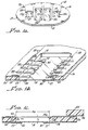
- FIGS. 1a through 1c illustrate a membrane probe embodying principles of the present invention.
- This probe is an improved version of the diaphragm test probe disclosed in the above-identified U.S. Patent No. 5,148,103.
- a flexible diaphragm, conductive contact pads and an arrangement for applying pressure to one side of the flexible diaphragm to accomplish self planarizing contact of the probe pads against the pads of a die or chip under test are features of the 5,148,103 patent as are a probe arrangement that adapts the probe for use in wafer testing processes using conventional pick and place loading and cassette storage of both membrane probes and test wafers.
- a typical wafer, of three to eight inches in diameter, for example, is formed with as many as several hundred individual dies, each of which has a width W d (Fig. 4a) of about 500 mils, and all positioned usually, but not necessarily in an array of columns of dies that are each spaced from all adjacent columns of dies on the wafer. It is desirable to test these dies on the wafer in as short a time as possible. Therefore it is desirable to enable simultaneous testing of all dies on the wafer, or at least of all dies of a group of dies on the wafer.
- FIGS. 1a through 1c An exemplary membrane probe test head configured for testing all dies in only two operations is illustrated in FIGS. 1a through 1c for purposes of explaining the present invention.
- the dies on a wafer are divided (operationally, but not physically) into two groups for use of a two test head probe set, or probe pair.
- the first group is composed of alternate columns of dies, such as the odd numbered columns illustrated in Fig. 4a as 56a, 56c, 56e and 56g, for example, and the second group is composed of the remaining dies, namely the even numbered columns (56b, 56d and 56f of Fig. 4b) which are interlaced between the odd numbered columns.
- a probe pair includes a first test head 10 uniquely configured for simultaneous testing of all dies of the first group of dies, and a second test head 110 uniquely (and differently) configured for simultaneous testing of all dies of the second group of dies.
- the probe pair 10,110 thus completely tests all chips on a full wafer with only two touchdowns of the probe, one for each test head of the probe pair.
- Test heads 10 and 110 of a probe pair are shown in FIGs. 4a and 4b respectively.
- Each of the probe tests heads 10,110 is formed of an electrically non-conductive rigid or semi-rigid and self supporting substrate 12,112 in the configuration of a generally flat, thin disc having multiple elongated ports 14,114 extending completely through the substrate and clad on both sides with thin layers of a transparent flexible dielectric such as polyimide layers 16,116 and 18,118.
- Ports on first test head 10 are numbered 14a, 14c, 14e and 14g to better portray the alternate row configuration of the test head.
- ports on second test head 110 are in like manner numbered 114b, 114d and 114f as shown in Fig. 4b.
- test head 10 For simplicity of explanation, the remainder of the discussion will address only test head 10, it being understood that the discussion applies as well to corresponding features of complementary test head 110, since the two test heads are identical except for the differences (to be described below) in the location and configuration of their elongated ports.
- Outer layer 18 extends across each port 14 but inner layer 16 does not, being of a configuration congruent with substrate 12 having apertures coextensive with substrate elongated ports 14 as illustrated in Fig. 1a.
- each port is closed on one (outer) side of the substrate by a layer, but is open on the other (inner) substrate side to admit air pressure, as will be described below.
- Those straight portions of substrate 12 immediately adjacent ports 14 are designated rib portions 20 and include those substrate portions separating adjacent ports from one another.
- a pattern of electrically conductive contact traces 22 is formed on one (outer) side of the substrate, upon polyimide layer 18. The contact traces extend from contact trace end portions disposed in a selected pattern upon the membrane 18 within the boundaries of each substrate port 14.
- the traces run generally perpendicular to substrate rib portions 20 and extend to a plurality of metallized vias (conduits) 24 that extend through the substrate and polyimide layers on each side, as seen in FIG.1b.
- the inner side of the probe test head, which bears the polyimide layer 16 carries on the periphery of the test head a plurality of relatively short, radially extending electrically conductive connector pads 26 (Figs. 1a and 1c) connected to signal traces 28 extending along rib portions 20.
- Each of these signal traces may be connected to one or more of the contact traces 22 by means of the appropriately located metallized substrate vias 24.
- connector pads 26 may be formed directly on the substrate 12, omitting layer 16.
- each contact trace opposite its substrate via bears an axially projecting contact pad, such as pads 30, such contact pads being positioned in a configuration that will match the pads of a circuit die that is to be tested.
- the contact pads are positioned on an unsupported area of the membrane within each port.
- the contact pads 30 are the lowest points of the probe, so that only these pads will contact a chip to be tested, particularly after the pads are displaced outwardly by air pressure applied to each port to bend the flexible membrane outwardly.
- Substrate 12 is formed preferably of a thin rigid photoceram material having a flat edge section 31 (FIG. 1a) formed on one side thereof to enable handling and orientation by well known, pick and place equipment, as will be described below.
- the entire membrane probe is dimensioned, configured and arranged to be handled by known pick and place equipment which may be substantially identical to equipment arranged to handle the wafers to be tested.
- the photoceram substrate 12 in the form of a solid, substantially rigid and self-supporting disc, is provided with a number of preformed holes to be used as the vias 24.
- the photoceram disc may have a diameter larger than the diameter of a standard wafer and may be six inches to ten inches in diameter, for example, having a thickness T s (Fig. 1c) of about 90 to 125 mils.
- T s Fig. 1c
- a thinner substrate will provide less support for the membrane segments stretched across each port, while a thicker substrate presents problems in filling of the vias with conductive material as described below.
- a layer of the membrane 16,18 is applied to each side of the photoceram substrate by employing standard spinning techniques in which a small amount of polyimide is placed on the photoceram surface and the disc spun to centrifugally distribute the polyimide evenly and radially outwardly. Several repetitions of this spinning process will build up the membrane thickness to provide a finished polyimide membrane of about 1 mil in thickness on each side of the photoceram substrate.
- the polyimide is highly transparent, as described in my above-identified patent 5,148,103 to enable visual registration of the membrane probe contact pads 30 with appropriate pads on the wafer die being tested.
- the spinning process is preferred because it yields a film that, although axially flexible within ports 14, is laterally taut across the relatively narrow transverse span of a port 14 so that the film is dimensionally stable in the plane of the film but may be flexed outwardly by gas pressure, as will be described below.
- the contact traces 22 and contact pads 30 are formed on one side of the substrate, on membrane 18.
- the connector pads 26 are then formed on the other side and the ports 14 are formed in the photoceram and also in the inner polyimide layer 16 but not in outer layer 18.
- a metal such as a mixture of tungsten with a small amount of titanium, W(Ti)
- W(Ti) titanium
- the vias may be filled with silver glass frit to provide superior conductivity.
- the entire lower surface, except for those areas at the end of traces 22 that are to be covered by contact pads 30, is coated with a dielectric passivation layer (not shown), which may be of a polyimide, to effectively electrically insulate the conductive trace surfaces.
- the contact pads 30 are plated (up to a height of 1 mil above traces 22, for example) on the ends of contact traces 22. If deemed necessary or desirable the contact pads finally may be flash coated with a highly stable conductive material such as a nickel-gold flash coating.
- photolithography employing suitable application of resist, development of the resist and removal of the undeveloped resist, is then employed to first sputter a thin metal coating on inner layer 16 in the desired pattern of connector pads 26 which then may be copper plated to provide a plurality of connecting pads (about 1 mil high) that extend in closely spaced relation circumferentially around the periphery of the inner side of the membrane probe, as can be best seen in FIG. 1a.
- Each of these pads is connected to a signal trace 28 that extends to a metallized via 24 so that at least some peripheral connector pads are electrically connected by way of such vias to associated ones of the contact traces 22.
- power and ground traces may be formed on the surface of polyimide layer 16, on an adjacent polyimide layer (not shown), or on a layer or layers (not shown) adjacent outer membrane 18. These power and ground traces may then be connected to connector pads 26 in the manner described above.
- electrical circuit elements may be mounted on the probe 10 and supported by the substrate 12 rigid surface, such as, for example, thin film resistor 29 (Fig. 1b) for isolating a power or data trace from a shorted chip 37 (Fig. 4a).
- the several elongated ports 14 are etched through the central region of substrate 12 (and through layer 16), resulting in the final probe configuration illustrated in FIGS. 1a and 1b.
- the result is a thin, relatively rigid, self-supporting disc having a flat edge 31 for orientation by automatic handling equipment and thin, flexible, taut, transparent port membranes 18 to the outer side of which are affixed the projecting probe contact pads 30 in a selected pattern that matches the pattern of pads on a grouping of alternate columns of dies to be tested.
- each die of a column of dies has a set of fifty contact pads and there are fifty dies in a column
- the portion of membrane 18 that is stretched across that port that corresponds to the particular column of dies will have fifty sets of membrane contact pads with fifty pads in each set, all configured so that in a single touchdown of the test head to the wafer, each pad of each die of the column will be contacted by a membrane pad.
- the other (inner) side of the probe test head has an annular array of connector pads 26, all lying in a single plane on the periphery of the test head, and a flat port-surrounding surface 32 (FIG. 4a) defining the test head area between the connector pads 26 and elongated ports 14 and including the area between the ports.
- Surface 32 comprising all of the probe substrate surface except for areas taken up by pads 26 and the ports (and their sealing O-rings), is used for vacuum attachment of the probe test head, as will be described below.
- the configuration of the ports and their grouping is specifically chosen to match the configuration of a column of dies and the configuration of a group of alternate columns in the illustrated arrangement. For example, if the aspect ratio of the dies on the wafer is such that the width (W d ) of a die is substantially less than its length, the distance between columns (i.e., vertical arrangement of FIG. 4a) is relatively narrower than the distance between rows (i.e., horizontal arrangement) of the same dies. Consequently, an arrangement of ports 14 spaced on alternate columns (FIG.
- probe 10 may be configured to space ports 14 on alternate rows rather than alternate columns to provide desirably wider ribs 20 under the described conditions.
- reference herein is made generally to columns of dies, but it will be understood that the description applies equally to rows of dies.
- the illustrated membrane probe may be used with many different types of testers and test fixtures. It is preferably used with application of a suitable pressure, such as a gas pressure, against the inner surfaces of the flexible transparent membrane 18 within elongated ports 14.
- a suitable pressure such as a gas pressure
- the probe illustrated is specifically designed for use in a test fixture to which the probe may be readily mechanically and electrically connected and disconnected, either manually or by automatic machines.
- both electrical and mechanical connection of the probe to a test fixture are accomplished in coordination with the configuration of the inner surface of the probe.
- This inner surface of the probe test head includes the connector pads 26 that form a substantially circular array around the periphery of the inner side of the test head, and the flat inwardly facing surface 32 (FIG.
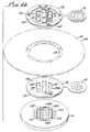
- This flat surface 32 is configured and arranged to enable vacuum attachment of the membrane to a test fixture insert 34 of a test fixture 50, shown in FIGS. 2a, 2b and 3.
- FIG. 3 Illustrated in FIG. 3 is a test fixture, generally indicated at 50, fixedly mounted to and above a support 52 that carries a movable work table 54 on which is mounted a test wafer 56 bearing dies that are to be tested by a membrane probe test head 10.
- the latter may be of the configuration illustrated in FIGS. 1a and 1b.
- the work table is movable in X,Y and Z, that is, in two perpendicular directions horizontally, and in one direction vertically by suitable manually controllable means (not shown).
- a rigid mounting plate 58 is fixedly carried on support 52 and has a central aperture defined by a radially inwardly directed lip 59 which supports a circumferential radially outwardly extending flange 60 of a test fixture insert 34 including a gas chamber housing 62.
- Housing 62 is circular in horizontal section and includes vertical partitioning members 90 forming walls 92 of elongated communicating pressure chambers 94 corresponding to and generally slightly larger in horizontal cross section than the elongated ports 14 of test head 10.
- Pressure chambers 94 are closed and sealed at their upper ends by a clear, transparent glass window 68 held in place by a retainer ring 72.
- Chamber housing 62 has a planar annular lower surface defining an annular peripheral seating rim 66 that defines a recess 70 congruent with the surface portion 32 of probe test head 10, i.e., that portion of the probe surface that lies radially between the connector pads 26 and the boundaries of elongated ports 14 of the test head including the probe surface between the ports.
- Recess 70 enclosed by the bottom surface rim 66 of the chamber housing 62 and test head surface portion 32 is connected by a conduit 74 to a source of vacuum (not shown) so as to firmly affix the probe test head 10 to the bottom surface of housing 62 in a gas tight sealing relation when vacuum is applied through the conduit.
- a source of vacuum not shown
- An angulated gas conduit 76 formed at and extending through one side of the housing 62, connects to the interior of all pressure chambers 94.
- Conduit 76 is adapted to be connected by means of a fitting 78 to a source of pressurized gas, such as air, which will apply a pressure to and within all communicating chambers 94 in the order of two to four pounds per square inch, thereby causing flexible membrane layer 18 to flex outwardly within each elongated port.
- Pressure chambers 94 all are sealed to window 68 by window O-ring seals 69 positioned between the window and partitioning members 90.
- the pressure chambers are in fluid communication with one another by accessible portions of conduit 76 extending through input partitions 90 as shown in Fig. 2b.
- the large area vacuum chamber 70 is isolated from the pressurized communicating chambers 94 in test fixture 34 by vacuum O-ring seals 71 mounted in partitioning members 90 and bearing against peripheral edges of the test head ports.
- vacuum O-ring seals 71 mounted in partitioning members 90 and bearing against peripheral edges of the test head ports.
- a multilevel printed circuit board 80 as shown in FIG. 3 is fixedly secured to the fixture mounting plate 58 as by mechanical fasteners, clamps or adhesive (not shown). Leads on the printed circuit board 80 are connected to an elastomeric electrical connector 84 in the form of an annular metal-on-elastomer ring known as an annular MOE.
- the MOE comprises a suitable elastomer, such as a silicon sponge, that has a plurality of circumferentially spaced, closely positioned, narrow metal connector elements positioned thereon as shown in my prior patent 5,148,103.
- the connector elements of the MOE and the connector pads 26 of the probe test head are positioned to mate with one another when the membrane probe test head is secured by the vacuum of annular recess 70 to the test fixture housing 62.
- a middle level of printed circuit board 80 is radially set back to provide a recess that receives the MOE 84 as best seen in FIG 3.
- MOE 84 includes elongated electrically conductive connector elements 86 (FIG 1c) on its lower surface which contact the connector pads 26 of the membrane probe and also the signal leads of the multi-level printed circuit board.
- the MOE also includes elongated contact strips on its upper surface which contact ground traces of the printed circuit board, thereby electrically connecting the membrane probe to the test fixture. Suitable electrical connections in the form of vias (not shown) extending through the MOE connect the elongated strips on its upper surface to associated connector pads 26 on the membrane probe test head.
- the signal leads and ground leads of the circuit board are coupled to testing circuitry by means of circuit connectors 82 (FIG. 3).
- FIG. 4a Shown in the pictorial view of FIG. 4a are the probe test head 10 and the work table 54.
- the table temporarily but fixedly supports the wafer 56 which is to be tested.
- the small rectangular dots indicated at 36 on the wafer 56 represent die pads of the chips or dies 37 that are to be tested.
- the dies are actually separated from one another on the wafer so that they can be individually severed.
- the die pads of each die define a pattern that is precisely matched by respective ones of each pattern of contact pads of the test head 10.
- the number and pattern of test head contact pads on all ports of one test head is the same as the number and pattern of die pads of all dies in alternate columns of dies on the wafer so that all dies can be contacted in two touchdowns of the membrane probe, one for each test head 10,110 in the membrane probe pair.
- port 14a covers die column 56a
- port 14c covers die column 56c
- port 14e covers die column 56e
- port 14g covers die column 56g, in the illustrated exemplary configuration.
- the ports of the second test head 110 of a pair respectively cover each of the die columns not covered by a port of first test head 10.
- a prime purpose of narrowing the span of the membrane within a port is to overcome the membrane sag or drape that is characteristic of the wider span of the prior art. It is desirable, therefore, to keep the width W p (Fig. 1c) of such a port 14 to a minimum, preferably not much greater than the width of a single die in the column of dies covered by the port.
- the membrane contact pads must lie on a membrane segment that is between the edges of a port, the port can be no narrower than the width between contact pads of such a die, and in fact must be at least wide enough to allow for sufficient distance between the edge of the port and the die contact pads to permit the membrane to flex downward to the die pads where air pressure is applied via the insert to the test head ports.
- Fig. 4a illustrates the critical distances just described.
- the membrane distance D d from one edge of the port (e.g. 14c) to its adjacent die column (e.g., 56c) edge is preferably about 60 mils to provide sufficient downward membrane displacement in the exemplary embodiment. Since the die pads 37 are inset within the die in the order of 5 to 10 mils from the edge of the die, the distance D c from the edge of the port to the center of the die pad is D d plus the 5-10 mils die inset distance, or a total D c of about 65 to 70 mils, which determines and corresponds to the length of contact traces 22 from the port edge to contact pads 30 in Fig. 1c.
- membrane distance D d is required on both sides of die column 56c, so that the total width W p of port 14c, for example, is the width of the die column 56c (500 mils) plus the sum of the membrane distances D d on either side of the die column 56c (120 mils) or about 620 mils.
- the port width is not greater than one and one-half times the die width and the port length is not less than an integral number of die lengths, so as to minimize drape and still allow simultaneous testing of a number of dies.
- the metal-on-elastomer (MOE) fixture connector 84 affords a simple, rapid detachable electrical connection between the test fixture printed circuit board 80 and connector pads on the membrane probe test head 10.
- the test head is formed with its circular peripheral array of connector pads 26, which mate with the circular array of the connector elements of the MOE.
- the resilient elasticity of the MOE ensures good electrical contact of all connector pads when the test head is pressed upwardly against the fixture by means of the applied vacuum.
- the resilient support and mounting of the MOE connector elements may readily deflect individually relative to one another when contacted by the associated connector pads 26 of the membrane probe test head to assure good firm, but detachable, electrical connection of the test head to the test fixture and to ensure planarity so that all connector pads will be in good electrical contact.
- a wafer cassette storage device stores a plurality of test wafers (bearing dies to be tested) which may be selectively extracted by a conventional type of pick and place machine.
- a test wafer is extracted from a wafer storage cassette and placed on the work table 54 of the test fixture.
- a second cassette storage device stores a number of different membrane probe test heads, all of which have the same mechanical size but which differ from one another by different patterns of traces and contact pads.
- a test fixture insert 34 or 134 corresponding to a selected test head 10 or 110 is manually installed as by suitable mechanical fasteners (not shown) in test fixture 50 as shown in FIG. 3.
- a second pick and place machine, or the same machine that was employed for emplacement of wafers 56, is arranged to extract a selected membrane probe test head from a probe storage cassette and position it in test fixture insert 34 of the test fixture 50 for connection in the manner illustrated in FIGS. 3 and 4a.
- test fixture After the test probe has been positioned in contact with the elastomeric probe connector (MOE), vacuum is applied via conduit 74 to mechanically fix the probe test head to the test fixture, and the test wafer is moved upwardly to or toward a very light contact with the test head contact pads. Now the operator visually observes the contact pads, which are readily visible through the probe ports 14 and the transparent membrane 18 upon which the contact pads are mounted. While the operator observes relative registration of the probe contact pads 30 with the die pads 36, the table 54 and wafer 56 thereon are moved to precisely align the probe contact pads with the die pads of each chip 37. The table then may be slightly raised an additional amount to a point where the contact pads are barely or almost contacting the die pads, and gas pressure then is applied to the test fixture communicating gas chambers 94.
- the applied gas pressure on the thin flexible polyimide film stretched across each elongated port 14 forces the probe contact pads into contact with the wafer die pads, providing a high contact pressure and excellent registration consistency because of the taut span of the membrane in the transverse direction, i.e., across the narrow dimension of the port, while the flexibility of the membrane that carries the contact pads 30 provides a self planarization of the contact pads to ensure good firm electrical contact between each probe contact pad and its associated wafer die pad.
- a typical wafer may contain dozens or hundreds dies and therefore dozens or hundreds of groups of die pads.
- Each probe membrane test head contains sufficient groups of contact pads so that one group of alternate columns of chips on the wafer under test may be tested at a given time.
- the gas pressure is released from the pressure chambers 94 and the second test head of a probe pair is similarly installed in the test fixture along with its corresponding test fixture insert which is uniquely configured with a plurality of pressure chambers 94 in a pattern conforming to the pattern of ports in the second test head. Then the test of the remaining die groups (alternate die columns) is accomplished after repressurization of the test fixture insert communicating gas chambers.
- the test procedure itself after the appropriate contact is made between the test fixture and the wafer to be tested, can be carried out in an exceedingly short time because all dies of a plurality of columns of dies (e.g., substantially half of the total number of dies on the wafer) can be tested either simultaneously or one column or one die at a time, using only one touchdown of a single test head.
- the time required to properly position the test probe and wafer under test is considerably longer than the time required for the actual testing. Therefore, the ability to test many dies with only a single probe positioning effort is a major time saver.
- test fixture insert 34 for odd column testing is installed in one such test fixture
- test fixture insert 134 for even column testing is installed in the other such test fixture.
- the wafer under test is positioned in the first test fixture and tested as described above, then is moved by its pick and place machine to the second test fixture to complete the testing of the remaining columns of chips.
- only one test head of each probe pair need be stored in a designated cassette and handled by one pick and place machine, greatly decreasing the positioning and registration time and significantly facilitating visual registration so as to greatly increase the rate of testing.
- wafer and probe connection means are feasible which retain the pressurization aspects of the present invention for deflection of the membrane, but feature mechanical fasteners rather than vacuum attachment of the probe.
- test probe and fixture and the method of testing described herein have a great many advantages. These advantages include the capability of testing a full wafer having 10,000 to 30,000 contacts, including burn-in testing, in just two massive touchdowns of a membrane probe pair, a capability that was not available heretofore because of the inability to simultaneously connect to widely separated dies and die pads on the test wafer.
- the ability to successfully contact such die pads is now achieved through the novel employment of a multiplicity of elongated ports on a test head which overcomes the membrane sag problem while retaining the soft pad contact which causes less damage to die pads than needle or blade contacts of prior probe cards.
- Such utilizing of multiple ports provides the additional advantage of permitting traces and circuit elements to be placed on the rib portions of the substrate that surround the ports, in positions very close to the probe test contact pads.
- each port has at least one dimension that is not greater than about one and one half times the width of a single die on the wafer.
- the test head enables the testing of many dies with but one single touchdown, but still avoids the problem of membrane drape, or sag, which would otherwise cause a large unsupported area of membrane to sag and consequently make contact with other wafer parts and dies other than the dies under test.
- the outward pressurization of the membrane would effect varying and uncontrolled relative lateral displacement of different membrane areas, thus preventing precision alignment.
- the temperature coefficient of expansion of the substrate can be matched to the temperature coefficient of expansion of a wafer under test so that testing over an extended range of temperatures is possible. Without such matching of temperature coefficients of expansion, a different expansion of the test probe substrate and the wafer would cause serious misalignment or require use of different probes at different temperatures.
- the multiport feature of the present invention minimizes excessive drape or sag of the membrane, and the soft contact between the contact pads of the probe and the die pads causes considerably decreased wear on the probe contacts which require only routine cleaning and need not be frequently adjusted and readjusted.
Abstract
A probe is disclosed for simultaneously testing a grouping of integrated circuit chips formed adjacent one another in the grouping on a semiconductor wafer. Each chip has a longitudinal dimension and a transverse dimension. The probe comprises a substantially rigid substrate having at least one elongated port (14) formed therein, the port (14) having a width not greater than one and one half times the transverse dimension. A flexible transparent membrane (16) extends across the elongated port (14) at least with a segment thereof. A plurality of electrically conductive traces (22) is formed on the membrane (16). A plurality of contact pads (30) is formed on selective ones of the traces (22). The contact pads (30) are disposed within the segments of the membrane (16).
Description
- The present invention relates to testing of integrated circuits and more particularly concerns improved membrane probes.
- Integrated circuits or chips including conductive traces, electrical components, and active devices are fabricated in batches of large numbers of similar or identical circuits on a single wafer and then individually cut from the wafer for use. Because production techniques and processes are pushed to the limits of accuracy and repeatability, significant numbers of circuits fabricated on a single wafer may prove to be unacceptable or inoperable. Therefore, before each circuit is separated from the others by severing the wafer into its many component circuits for its intended use, it is desirable to test each circuit individually.
- Probe cards presently employed for testing of integrated circuits while still on the wafer employ a number of probe contact elements, commonly in the form of very small blades or needles that are mechanically and electrically fixed to a circuit board or the like and have leads that fan out to outer edges of the probe card for making connections between the probe card and testing circuitry. The contact blades or needles of the probe card are moved into contact with specific areas, namely the pads of the integrated circuit or chip under test, and may be electrically connected so as to apply selected input signals and to read output signals from the device under test. In this manner the chips are tested on the wafer, before being connected for intended use, by applying operating signals and monitoring and evaluating resultant outputs.
- In the use of such probe cards, the contact between the probe card blades or needles and the circuit chip is frequently made by a scrubbing action, which tends to deflect the slender probe elements as much as several mils on each touchdown. This displacement, which occurs repetitively upon each test, further tends to change the desired positioning of the elements.
- The probe may have from fifty to several hundred contacts, each of which must be precisely and individually positioned with respect to all others so that upon contact with the circuit chip all probe contacts will contact all pads of the chip under test. All of this means that the probe cards presently used are exceedingly expensive, require much maintenance, and are subject to many errors.
- As integrated circuit speeds increase, so too do the difficulty and extent of the testing problems. Such problems are caused by cross-talk between adjacent signal traces, signal loss and degradation due to capacitative loading of the circuit under test, and increased need for shielding and impedance matching of signal lines throughout the test fixture and test head. High frequency probe transmission lines must be properly terminated. Although high frequency hardware can be provided up to the test head itself, the physical connection between the test head and the integrated circuit pad, which relies upon exposed metallic blades or needles, provides poor high frequency performance and extremely fragile components. Thus the final part of the probe transmission line cannot be properly terminated.
- As size and spacing of integrated circuit chips decrease and density of chip contacts increases, it becomes ever more difficult to make mechanical blade or needle contacts as small and closely spaced as required for proper testing of modern integrated circuit chips. Moreover, the great bulk and complex configuration of prior art probe cards do not readily lend themselves to automated handling or simplified storage.
- My U.S. Patent No. 5,148,103 describing apparatus for testing integrated circuits has a number of features including employing a flexible diaphragm, conductive contact pads and an arrangement for applying pressure to one side of the flexible diaphragm to accomplish self planarizing contact of the probe pads against the pads of a die or chip under test. Patent 5,148,103 also provides probe arrangements that adapt the probe for use in wafer testing processes using conventional pick and place loading and cassette storage of both membrane probes and test wafers.
- However, neither the 5,148,103 patent nor any other known arrangement provides for economically fast full-wafer testing at high temperatures nor for a number of improvements that are available with the methods and apparatus described herein. Membranes of the prior art have a single port, which is not suitable for full wafer burn-in testing, i.e., simultaneous testing of all or substantial numbers of the hundreds of chips on a three, six or eight inch diameter wafer, because the deflection, or sag, of a large single membrane is too severe for chips, and even contacts, widely separated on the wafer. Although numerous attempts have been made by others to avoid excessive sag in the testing for individual chips (see, e.g., U.S. Patent No. 5,264,747 to Woith et al., assigned to the assignee of the present application), no suitable solution to the problem of simultaneous testing of plural chips has been known heretofore.
- Additionally, the diaphanous nature of the membrane in a single large aperture probe precludes mounting of the heavier circuit elements such as decoupling capacitors and isolating resistors within that central aperture, at points close to the test contacts.
- Accordingly, it is an object of the present invention to provide for multi-chip testing of integrated circuit chips while avoiding or minimizing the problems mentioned above.
- In carrying out principles of the present invention in accordance with an exemplary embodiment of one feature thereof, a plurality of columns or rows of integrated circuit chips formed on a single wafer are simultaneously tested by providing a test probe set. A test probe set consists of two or more test heads. In a specific embodiment, using only two test heads for a complete probe set, one test head is configured for testing chips in one grouping of alternate columns or rows of chips on a certain wafer, and the other is configured for testing chips in the remaining interleaved alternate columns or rows of chips on the same wafer. The probe sets corresponding to the configurations of different wafers are stored in a cassette. A membrane probe test fixture insert is installed in a test fixture for each test head configuration. A wafer containing chips to be tested is positioned adjacent a test fixture, and a pick and place machine is employed to selectively extract a chosen probe test head from the cassette and move it to the fixture to which it is detachably connected, both mechanically and electrically at the same time, to allow the probe test head to contact the chips of one grouping of chips to be tested.
- According to another feature of the invention, an individual test head of a probe set is formed of a substrate having elongated mutually spaced ports spatially corresponding to alternate columns or rows of chips on the wafer to be tested, and a flexible transparent membrane having a pattern of electrically conductive traces formed on the membrane. A plurality of contact pads are formed on selected ones of the traces, the contact pads being visually accessible through the substrate elongated ports. Connector pads on the membrane are connected to the traces to facilitate rapid detachable electrical connection to a test fixture.
- According to other features of the invention, the test head membrane may have a terminating resistor for terminating a high frequency transmission line or may have a buffer chip to provide high impedance, low capacitance loading. These and other circuit elements may be mounted on the substrate ribs, i.e., the material between and separating the elongated ports. Multiple layers of a test head membrane may be employed to attain complex geometry of probe contact pads and trace patterns.
- In the accompanying drawings:
- FIG. 1a is a pictorial view of one membrane probe test head of a pair of test heads embodying principles of the present invention;
- FIG. 1b is an enlarged pictorial view, partly in cross section of part of the probe test head of FIG. 1a;
- FIG. 1c is a cross section view of a peripheral portion of the probe test head of FIG. 1a;
- FIG. 2a is a pictorial view of a test fixture insert of the present invention;
- FIG. 2b is a cross section taken on
line 2b-2b of FIG. 2a; - FIG. 3 is a sectional view of a test fixture and work table for testing integrated circuit chips of a wafer;
- FIG. 4a is a pictorial view with parts exploded of the test fixture and work table of FIG.3 showing one of two test heads of a probe pair and its insert; and
- FIG. 4b is a pictorial view with parts exploded of the test fixture and work table of FIG.3 like FIG. 4a, but showing the other of two test heads of a probe pair and its insert.
- FIGS. 1a through 1c illustrate a membrane probe embodying principles of the present invention. This probe is an improved version of the diaphragm test probe disclosed in the above-identified U.S. Patent No. 5,148,103. A flexible diaphragm, conductive contact pads and an arrangement for applying pressure to one side of the flexible diaphragm to accomplish self planarizing contact of the probe pads against the pads of a die or chip under test are features of the 5,148,103 patent as are a probe arrangement that adapts the probe for use in wafer testing processes using conventional pick and place loading and cassette storage of both membrane probes and test wafers.
- Significant improvements of the present invention over the prior art include a multiport configuration of probe test heads that overcomes membrane sag or drape to advantageously permit an entire column or row, or a group of entire columns or rows, either odd or even, of integrated circuit chips on the wafer to be contacted and tested during one massive touchdown of a probe test head. Additionally, the more rigid nature of the probe central region surrounding and separating the probe ports allows mounting of circuit components such as high current leads, decoupling capacitors and isolating resistors within that supportive probe central region.
- A typical wafer, of three to eight inches in diameter, for example, is formed with as many as several hundred individual dies, each of which has a width Wd (Fig. 4a) of about 500 mils, and all positioned usually, but not necessarily in an array of columns of dies that are each spaced from all adjacent columns of dies on the wafer. It is desirable to test these dies on the wafer in as short a time as possible. Therefore it is desirable to enable simultaneous testing of all dies on the wafer, or at least of all dies of a group of dies on the wafer.
- An exemplary membrane probe test head configured for testing all dies in only two operations is illustrated in FIGS. 1a through 1c for purposes of explaining the present invention. The dies on a wafer are divided (operationally, but not physically) into two groups for use of a two test head probe set, or probe pair. The first group is composed of alternate columns of dies, such as the odd numbered columns illustrated in Fig. 4a as 56a, 56c, 56e and 56g, for example, and the second group is composed of the remaining dies, namely the even numbered columns (56b, 56d and 56f of Fig. 4b) which are interlaced between the odd numbered columns. A probe pair includes a
first test head 10 uniquely configured for simultaneous testing of all dies of the first group of dies, and asecond test head 110 uniquely (and differently) configured for simultaneous testing of all dies of the second group of dies. The probe pair 10,110 thus completely tests all chips on a full wafer with only two touchdowns of the probe, one for each test head of the probe pair. Test heads 10 and 110 of a probe pair are shown in FIGs. 4a and 4b respectively. - Each of the probe tests heads 10,110 is formed of an electrically non-conductive rigid or semi-rigid and self supporting substrate 12,112 in the configuration of a generally flat, thin disc having multiple elongated ports 14,114 extending completely through the substrate and clad on both sides with thin layers of a transparent flexible dielectric such as polyimide layers 16,116 and 18,118. Ports on
first test head 10 are numbered 14a, 14c, 14e and 14g to better portray the alternate row configuration of the test head. Accordingly, ports onsecond test head 110 are in like manner numbered 114b, 114d and 114f as shown in Fig. 4b. - For simplicity of explanation, the remainder of the discussion will address only test
head 10, it being understood that the discussion applies as well to corresponding features ofcomplementary test head 110, since the two test heads are identical except for the differences (to be described below) in the location and configuration of their elongated ports. -
Outer layer 18 extends across eachport 14 butinner layer 16 does not, being of a configuration congruent withsubstrate 12 having apertures coextensive with substrate elongatedports 14 as illustrated in Fig. 1a. Thus each port is closed on one (outer) side of the substrate by a layer, but is open on the other (inner) substrate side to admit air pressure, as will be described below. Those straight portions ofsubstrate 12 immediatelyadjacent ports 14 are designatedrib portions 20 and include those substrate portions separating adjacent ports from one another. A pattern of electrically conductive contact traces 22 is formed on one (outer) side of the substrate, uponpolyimide layer 18. The contact traces extend from contact trace end portions disposed in a selected pattern upon themembrane 18 within the boundaries of eachsubstrate port 14. The traces run generally perpendicular tosubstrate rib portions 20 and extend to a plurality of metallized vias (conduits) 24 that extend through the substrate and polyimide layers on each side, as seen in FIG.1b. The inner side of the probe test head, which bears thepolyimide layer 16, carries on the periphery of the test head a plurality of relatively short, radially extending electrically conductive connector pads 26 (Figs. 1a and 1c) connected to signaltraces 28 extending alongrib portions 20. Each of these signal traces may be connected to one or more of the contact traces 22 by means of the appropriately located metallizedsubstrate vias 24. Alternatively,connector pads 26 may be formed directly on thesubstrate 12, omittinglayer 16. The end of each contact trace opposite its substrate via bears an axially projecting contact pad, such aspads 30, such contact pads being positioned in a configuration that will match the pads of a circuit die that is to be tested. Thus the contact pads are positioned on an unsupported area of the membrane within each port. In use of the probe, with theouter layer 18 facing downwardly, thecontact pads 30 are the lowest points of the probe, so that only these pads will contact a chip to be tested, particularly after the pads are displaced outwardly by air pressure applied to each port to bend the flexible membrane outwardly. -
Substrate 12 is formed preferably of a thin rigid photoceram material having a flat edge section 31 (FIG. 1a) formed on one side thereof to enable handling and orientation by well known, pick and place equipment, as will be described below. The entire membrane probe is dimensioned, configured and arranged to be handled by known pick and place equipment which may be substantially identical to equipment arranged to handle the wafers to be tested. - In manufacture of the described membrane probe test head the
photoceram substrate 12, in the form of a solid, substantially rigid and self-supporting disc, is provided with a number of preformed holes to be used as thevias 24. Preferably the photoceram disc may have a diameter larger than the diameter of a standard wafer and may be six inches to ten inches in diameter, for example, having a thickness Ts (Fig. 1c) of about 90 to 125 mils. A thinner substrate will provide less support for the membrane segments stretched across each port, while a thicker substrate presents problems in filling of the vias with conductive material as described below. A layer of themembrane probe contact pads 30 with appropriate pads on the wafer die being tested. Although the polyimide film may be applied in various ways, the spinning process is preferred because it yields a film that, although axially flexible withinports 14, is laterally taut across the relatively narrow transverse span of aport 14 so that the film is dimensionally stable in the plane of the film but may be flexed outwardly by gas pressure, as will be described below. - After application of the polyimide film to both sides, the contact traces 22 and
contact pads 30 are formed on one side of the substrate, onmembrane 18. Theconnector pads 26 are then formed on the other side and theports 14 are formed in the photoceram and also in theinner polyimide layer 16 but not inouter layer 18. To perform these steps, after photolithographically applying resist in a suitable pattern to theouter polyimide layer 18, a metal such as a mixture of tungsten with a small amount of titanium, W(Ti), is sputtered over the entire surface including the resist and vias, and the resist (and portions of the sputtered metal) is then lifted to leave a pattern of thin, sputtered traces forming the pattern of contact traces 22 on thepolyimide layer 18. The contact traces 22, which may be formed of copper, for example, are then electrolytically plated upon the pattern of sputtered-on metal traces, at the same time metallizing the interior of thevias 24. The vias may be filled with silver glass frit to provide superior conductivity. Then the entire lower surface, except for those areas at the end oftraces 22 that are to be covered bycontact pads 30, is coated with a dielectric passivation layer (not shown), which may be of a polyimide, to effectively electrically insulate the conductive trace surfaces. Now, using photolithography, masking and applying resist, thecontact pads 30 are plated (up to a height of 1 mil above traces 22, for example) on the ends of contact traces 22. If deemed necessary or desirable the contact pads finally may be flash coated with a highly stable conductive material such as a nickel-gold flash coating. - Similarly, photolithography, employing suitable application of resist, development of the resist and removal of the undeveloped resist, is then employed to first sputter a thin metal coating on
inner layer 16 in the desired pattern ofconnector pads 26 which then may be copper plated to provide a plurality of connecting pads (about 1 mil high) that extend in closely spaced relation circumferentially around the periphery of the inner side of the membrane probe, as can be best seen in FIG. 1a. Each of these pads is connected to asignal trace 28 that extends to a metallized via 24 so that at least some peripheral connector pads are electrically connected by way of such vias to associated ones of the contact traces 22. In addition, power and ground traces (not shown) may be formed on the surface ofpolyimide layer 16, on an adjacent polyimide layer (not shown), or on a layer or layers (not shown) adjacentouter membrane 18. These power and ground traces may then be connected toconnector pads 26 in the manner described above. In addition, electrical circuit elements may be mounted on theprobe 10 and supported by thesubstrate 12 rigid surface, such as, for example, thin film resistor 29 (Fig. 1b) for isolating a power or data trace from a shorted chip 37 (Fig. 4a). - After forming the conductive traces on both sides of the membrane probe by suitable masking and application of resist, the several elongated
ports 14 are etched through the central region of substrate 12 (and through layer 16), resulting in the final probe configuration illustrated in FIGS. 1a and 1b. The result is a thin, relatively rigid, self-supporting disc having aflat edge 31 for orientation by automatic handling equipment and thin, flexible, taut,transparent port membranes 18 to the outer side of which are affixed the projectingprobe contact pads 30 in a selected pattern that matches the pattern of pads on a grouping of alternate columns of dies to be tested. For example, if each die of a column of dies has a set of fifty contact pads and there are fifty dies in a column, the portion ofmembrane 18 that is stretched across that port that corresponds to the particular column of dies will have fifty sets of membrane contact pads with fifty pads in each set, all configured so that in a single touchdown of the test head to the wafer, each pad of each die of the column will be contacted by a membrane pad. - The other (inner) side of the probe test head has an annular array of
connector pads 26, all lying in a single plane on the periphery of the test head, and a flat port-surrounding surface 32 (FIG. 4a) defining the test head area between theconnector pads 26 andelongated ports 14 and including the area between the ports.Surface 32, comprising all of the probe substrate surface except for areas taken up bypads 26 and the ports (and their sealing O-rings), is used for vacuum attachment of the probe test head, as will be described below. - Although only four mutually opposed and parallel ports are shown, other numbers and configurations of ports may be used as deemed necessary or desirable. The configuration of the ports and their grouping is specifically chosen to match the configuration of a column of dies and the configuration of a group of alternate columns in the illustrated arrangement. For example, if the aspect ratio of the dies on the wafer is such that the width (Wd) of a die is substantially less than its length, the distance between columns (i.e., vertical arrangement of FIG. 4a) is relatively narrower than the distance between rows (i.e., horizontal arrangement) of the same dies. Consequently, an arrangement of
ports 14 spaced on alternate columns (FIG. 4a) will result in a rib width (Wr) narrower than would result from an arrangement ofports 14 spaced on alternate rows. Accordingly, probe 10 may be configured tospace ports 14 on alternate rows rather than alternate columns to provide desirablywider ribs 20 under the described conditions. For simplicity in explanation, reference herein is made generally to columns of dies, but it will be understood that the description applies equally to rows of dies. - The illustrated membrane probe may be used with many different types of testers and test fixtures. It is preferably used with application of a suitable pressure, such as a gas pressure, against the inner surfaces of the flexible
transparent membrane 18 withinelongated ports 14. However, the probe illustrated is specifically designed for use in a test fixture to which the probe may be readily mechanically and electrically connected and disconnected, either manually or by automatic machines. In the illustrated probe configuration, both electrical and mechanical connection of the probe to a test fixture are accomplished in coordination with the configuration of the inner surface of the probe. This inner surface of the probe test head includes theconnector pads 26 that form a substantially circular array around the periphery of the inner side of the test head, and the flat inwardly facing surface 32 (FIG. 4a) ofpolyimide layer 16 that extends between theconnector pads 26 and the boundaries of theelongated ports 14 that extend through the substrate. Thisflat surface 32 is configured and arranged to enable vacuum attachment of the membrane to atest fixture insert 34 of atest fixture 50, shown in FIGS. 2a, 2b and 3. - Illustrated in FIG. 3 is a test fixture, generally indicated at 50, fixedly mounted to and above a
support 52 that carries a movable work table 54 on which is mounted atest wafer 56 bearing dies that are to be tested by a membraneprobe test head 10. The latter may be of the configuration illustrated in FIGS. 1a and 1b. The work table is movable in X,Y and Z, that is, in two perpendicular directions horizontally, and in one direction vertically by suitable manually controllable means (not shown). - As can be seen in FIGs. 2b and 3, a rigid mounting
plate 58 is fixedly carried onsupport 52 and has a central aperture defined by a radially inwardly directedlip 59 which supports a circumferential radially outwardly extendingflange 60 of atest fixture insert 34 including agas chamber housing 62.Housing 62 is circular in horizontal section and includesvertical partitioning members 90 formingwalls 92 of elongated communicatingpressure chambers 94 corresponding to and generally slightly larger in horizontal cross section than theelongated ports 14 oftest head 10.Pressure chambers 94 are closed and sealed at their upper ends by a clear, transparent glass window 68 held in place by aretainer ring 72.Chamber housing 62 has a planar annular lower surface defining an annular peripheral seating rim 66 that defines arecess 70 congruent with thesurface portion 32 ofprobe test head 10, i.e., that portion of the probe surface that lies radially between theconnector pads 26 and the boundaries ofelongated ports 14 of the test head including the probe surface between the ports. -
Recess 70, enclosed by the bottom surface rim 66 of thechamber housing 62 and testhead surface portion 32 is connected by a conduit 74 to a source of vacuum (not shown) so as to firmly affix theprobe test head 10 to the bottom surface ofhousing 62 in a gas tight sealing relation when vacuum is applied through the conduit. Thus the membrane test head is attached in a readily attachable and detachable fashion to the test fixture. - An angulated
gas conduit 76, formed at and extending through one side of thehousing 62, connects to the interior of allpressure chambers 94.Conduit 76 is adapted to be connected by means of a fitting 78 to a source of pressurized gas, such as air, which will apply a pressure to and within all communicatingchambers 94 in the order of two to four pounds per square inch, thereby causingflexible membrane layer 18 to flex outwardly within each elongated port.Pressure chambers 94 all are sealed to window 68 by window O-ring seals 69 positioned between the window andpartitioning members 90. The pressure chambers are in fluid communication with one another by accessible portions ofconduit 76 extending throughinput partitions 90 as shown in Fig. 2b. The largearea vacuum chamber 70 is isolated from the pressurized communicatingchambers 94 intest fixture 34 by vacuum O-ring seals 71 mounted inpartitioning members 90 and bearing against peripheral edges of the test head ports. Thus the probe attaching vacuum extends around and between the ports whereas the membrane distending positive pressure is confined to the areas within the ports. - For readily detachable and attachable electrical connection of the test head to the test fixture, a multilevel printed
circuit board 80 as shown in FIG. 3 is fixedly secured to thefixture mounting plate 58 as by mechanical fasteners, clamps or adhesive (not shown). Leads on the printedcircuit board 80 are connected to an elastomericelectrical connector 84 in the form of an annular metal-on-elastomer ring known as an annular MOE. The MOE comprises a suitable elastomer, such as a silicon sponge, that has a plurality of circumferentially spaced, closely positioned, narrow metal connector elements positioned thereon as shown in my prior patent 5,148,103. The connector elements of the MOE and theconnector pads 26 of the probe test head are positioned to mate with one another when the membrane probe test head is secured by the vacuum ofannular recess 70 to thetest fixture housing 62. - A middle level of printed
circuit board 80 is radially set back to provide a recess that receives theMOE 84 as best seen in FIG 3.MOE 84 includes elongated electrically conductive connector elements 86 (FIG 1c) on its lower surface which contact theconnector pads 26 of the membrane probe and also the signal leads of the multi-level printed circuit board. The MOE also includes elongated contact strips on its upper surface which contact ground traces of the printed circuit board, thereby electrically connecting the membrane probe to the test fixture. Suitable electrical connections in the form of vias (not shown) extending through the MOE connect the elongated strips on its upper surface to associatedconnector pads 26 on the membrane probe test head. The signal leads and ground leads of the circuit board are coupled to testing circuitry by means of circuit connectors 82 (FIG. 3). - Shown in the pictorial view of FIG. 4a are the
probe test head 10 and the work table 54. The table temporarily but fixedly supports thewafer 56 which is to be tested. The small rectangular dots indicated at 36 on thewafer 56 represent die pads of the chips or dies 37 that are to be tested. The dies are actually separated from one another on the wafer so that they can be individually severed. The die pads of each die define a pattern that is precisely matched by respective ones of each pattern of contact pads of thetest head 10. The number and pattern of test head contact pads on all ports of one test head is the same as the number and pattern of die pads of all dies in alternate columns of dies on the wafer so that all dies can be contacted in two touchdowns of the membrane probe, one for each test head 10,110 in the membrane probe pair. For example, as shown by the dotted lines in FIG 4a, port 14a covers die column 56a, port 14c covers die column 56c,port 14e covers diecolumn 56e and port 14g covers die column 56g, in the illustrated exemplary configuration. The ports of thesecond test head 110 of a pair respectively cover each of the die columns not covered by a port offirst test head 10. - As noted earlier, a prime purpose of narrowing the span of the membrane within a port is to overcome the membrane sag or drape that is characteristic of the wider span of the prior art. It is desirable, therefore, to keep the width Wp (Fig. 1c) of such a
port 14 to a minimum, preferably not much greater than the width of a single die in the column of dies covered by the port. However, because the membrane contact pads must lie on a membrane segment that is between the edges of a port, the port can be no narrower than the width between contact pads of such a die, and in fact must be at least wide enough to allow for sufficient distance between the edge of the port and the die contact pads to permit the membrane to flex downward to the die pads where air pressure is applied via the insert to the test head ports. Fig. 4a illustrates the critical distances just described. - For a typical die width Wd, (Fig. 4a) of 500 mils, the membrane distance Dd from one edge of the port (e.g. 14c) to its adjacent die column (e.g., 56c) edge is preferably about 60 mils to provide sufficient downward membrane displacement in the exemplary embodiment. Since the
die pads 37 are inset within the die in the order of 5 to 10 mils from the edge of the die, the distance Dc from the edge of the port to the center of the die pad is Dd plus the 5-10 mils die inset distance, or a total Dc of about 65 to 70 mils, which determines and corresponds to the length of contact traces 22 from the port edge to contactpads 30 in Fig. 1c. - As can be seen in Fig. 4a, membrane distance Dd is required on both sides of die column 56c, so that the total width Wp of port 14c, for example, is the width of the die column 56c (500 mils) plus the sum of the membrane distances Dd on either side of the die column 56c (120 mils) or about 620 mils. A
typical rib 20, therefore, separating forexample ports 14c and 14e, will have a width Wr equal to the width Wd of a die minus the sum of the membrane distances Dd on either side of the rib, i.e.,
typical rib 20. These dimensions provide the necessary balance between increased substrate rigidity for optimum membrane sag minimization and component support on the one hand, and the necessary membrane flexibility on the other hand to permit themembrane contact pads 30 to be displaced under pressure so as to mate positively with thedie contact pads 37. In general the port width is not greater than one and one-half times the die width and the port length is not less than an integral number of die lengths, so as to minimize drape and still allow simultaneous testing of a number of dies. - Referring again to FIG. 3, the metal-on-elastomer (MOE)
fixture connector 84 affords a simple, rapid detachable electrical connection between the test fixture printedcircuit board 80 and connector pads on the membraneprobe test head 10. The test head is formed with its circular peripheral array ofconnector pads 26, which mate with the circular array of the connector elements of the MOE. The resilient elasticity of the MOE ensures good electrical contact of all connector pads when the test head is pressed upwardly against the fixture by means of the applied vacuum. Because of the resilient support and mounting of the MOE connector elements, they may readily deflect individually relative to one another when contacted by the associatedconnector pads 26 of the membrane probe test head to assure good firm, but detachable, electrical connection of the test head to the test fixture and to ensure planarity so that all connector pads will be in good electrical contact. - The described arrangement of fixture and membrane probe readily lend themselves to automatic test operation in a well-known pick and place system. In such an automatic system a wafer cassette storage device stores a plurality of test wafers (bearing dies to be tested) which may be selectively extracted by a conventional type of pick and place machine. A test wafer is extracted from a wafer storage cassette and placed on the work table 54 of the test fixture.
- Similarly, a second cassette storage device stores a number of different membrane probe test heads, all of which have the same mechanical size but which differ from one another by different patterns of traces and contact pads. A
test fixture insert test head test fixture 50 as shown in FIG. 3. A second pick and place machine, or the same machine that was employed for emplacement ofwafers 56, is arranged to extract a selected membrane probe test head from a probe storage cassette and position it intest fixture insert 34 of thetest fixture 50 for connection in the manner illustrated in FIGS. 3 and 4a. After the test probe has been positioned in contact with the elastomeric probe connector (MOE), vacuum is applied via conduit 74 to mechanically fix the probe test head to the test fixture, and the test wafer is moved upwardly to or toward a very light contact with the test head contact pads. Now the operator visually observes the contact pads, which are readily visible through theprobe ports 14 and thetransparent membrane 18 upon which the contact pads are mounted. While the operator observes relative registration of theprobe contact pads 30 with thedie pads 36, the table 54 andwafer 56 thereon are moved to precisely align the probe contact pads with the die pads of eachchip 37. The table then may be slightly raised an additional amount to a point where the contact pads are barely or almost contacting the die pads, and gas pressure then is applied to the test fixture communicatinggas chambers 94. The applied gas pressure on the thin flexible polyimide film stretched across eachelongated port 14 forces the probe contact pads into contact with the wafer die pads, providing a high contact pressure and excellent registration consistency because of the taut span of the membrane in the transverse direction, i.e., across the narrow dimension of the port, while the flexibility of the membrane that carries thecontact pads 30 provides a self planarization of the contact pads to ensure good firm electrical contact between each probe contact pad and its associated wafer die pad. - A typical wafer may contain dozens or hundreds dies and therefore dozens or hundreds of groups of die pads. Each probe membrane test head contains sufficient groups of contact pads so that one group of alternate columns of chips on the wafer under test may be tested at a given time. After completing a test on one group of dies, (e.g., all dies in one group of alternate columns of dies), the gas pressure is released from the
pressure chambers 94 and the second test head of a probe pair is similarly installed in the test fixture along with its corresponding test fixture insert which is uniquely configured with a plurality ofpressure chambers 94 in a pattern conforming to the pattern of ports in the second test head. Then the test of the remaining die groups (alternate die columns) is accomplished after repressurization of the test fixture insert communicating gas chambers. - The test procedure itself, after the appropriate contact is made between the test fixture and the wafer to be tested, can be carried out in an exceedingly short time because all dies of a plurality of columns of dies (e.g., substantially half of the total number of dies on the wafer) can be tested either simultaneously or one column or one die at a time, using only one touchdown of a single test head. In contrast, the time required to properly position the test probe and wafer under test is considerably longer than the time required for the actual testing. Therefore, the ability to test many dies with only a single probe positioning effort is a major time saver.
- It will be readily understood that two test fixtures may be employed for rapid parallel operation, wherein test fixture insert 34 (FIG. 4a) for odd column testing is installed in one such test fixture, while a test fixture insert 134 (FIG. 4b) for even column testing is installed in the other such test fixture. Accordingly, the wafer under test is positioned in the first test fixture and tested as described above, then is moved by its pick and place machine to the second test fixture to complete the testing of the remaining columns of chips. In this way, only one test head of each probe pair need be stored in a designated cassette and handled by one pick and place machine, greatly decreasing the positioning and registration time and significantly facilitating visual registration so as to greatly increase the rate of testing.
- Additionally, other methods of firmly securing the membrane probe test heads to the test fixture are contemplated. For example, wafer and probe connection means are feasible which retain the pressurization aspects of the present invention for deflection of the membrane, but feature mechanical fasteners rather than vacuum attachment of the probe.
- It will be readily appreciated that the test probe and fixture and the method of testing described herein have a great many advantages. These advantages include the capability of testing a full wafer having 10,000 to 30,000 contacts, including burn-in testing, in just two massive touchdowns of a membrane probe pair, a capability that was not available heretofore because of the inability to simultaneously connect to widely separated dies and die pads on the test wafer. The ability to successfully contact such die pads is now achieved through the novel employment of a multiplicity of elongated ports on a test head which overcomes the membrane sag problem while retaining the soft pad contact which causes less damage to die pads than needle or blade contacts of prior probe cards. Such utilizing of multiple ports provides the additional advantage of permitting traces and circuit elements to be placed on the rib portions of the substrate that surround the ports, in positions very close to the probe test contact pads.
- Importantly, each port has at least one dimension that is not greater than about one and one half times the width of a single die on the wafer. With this very small transverse dimension and a longitudinal dimension that is many times greater than the dimension of a single die (e.g., great enough to cover one full column of dies, or a full row of dies as noted earlier), the test head enables the testing of many dies with but one single touchdown, but still avoids the problem of membrane drape, or sag, which would otherwise cause a large unsupported area of membrane to sag and consequently make contact with other wafer parts and dies other than the dies under test. Moreover, with a large unsupported membrane area bearing several sets of contacts for plural dies on a wafer, the outward pressurization of the membrane would effect varying and uncontrolled relative lateral displacement of different membrane areas, thus preventing precision alignment.
- The temperature coefficient of expansion of the substrate can be matched to the temperature coefficient of expansion of a wafer under test so that testing over an extended range of temperatures is possible. Without such matching of temperature coefficients of expansion, a different expansion of the test probe substrate and the wafer would cause serious misalignment or require use of different probes at different temperatures.
- Manufacture of the probes described herein is much faster, more efficient, and less expensive since once the appropriate dies and masks for the photolithographic techniques employed have been manufactured it is relatively simple to manufacture a large number of membrane probes. This is to be distinguished from those probes employing needles and blades which must be individually adjusted on each probe. More importantly, the multiport feature of the present invention minimizes excessive drape or sag of the membrane, and the soft contact between the contact pads of the probe and the die pads causes considerably decreased wear on the probe contacts which require only routine cleaning and need not be frequently adjusted and readjusted.
- With the described membrane probe, alignment accuracy of 1 to 2 microns is possible with a high accuracy probe station that enables precision X,Y motion of the wafer under test. Having such high accuracy alignment, it is feasible to make and employ probe pads of less than 1 mil in diameter.
Claims (10)
- A probe for simultaneously testing a grouping (56a - 56g) of integrated circuit chips (37) formed adjacent one another in said grouping (56a - 56g) on a semiconductor wafer (56), each chip (37) having a longitudinal dimension and a transverse dimension, characterized by:- a substantially rigid substrate (12, 112) having at least one elongated port (14, 114) formed therein, said port (14, 114) having a width (Wp) not greater than one and one half times said transverse dimension;- a flexible transparent membrane (16, 18, 116, 118), at least a segment of which extending across said elongated port (14, 114);- a plurality of electrically conductive traces (22) formed on said membrane (16, 18, 116, 118); and- a plurality of contact pads (30) formed on selected ones of said traces (22), said contact pads (30) being disposed within said segment of said membrane (16, 18, 116, 118).
- The probe of claim 1, characterized in that said port (14, 16, 114, 116) has a length not less than an integral number of said longitudinal dimensions.
- The probe of claim 1 or 2, characterized in that said grouping (56a - 56g) of chips (37) includes at least two alternate columns of said chips (37) transversely spaced by an alternate column distance (Dc) and that said substrate (12, 112) further includes first and second elongated ports (14a - 14g, 114a - 114f) mutually spaced and corresponding to said alternate columns of chips (37), said second port also having a segment of said flexible membrane (16, 18, 116, 118) extending thereacross, said ports (14a - 14g, 114a - 114f) of each said substrate (12) being separated by a rib region of said substrate (12) having at least one rib (20), each said rib (20) having a width (Wr) less than said alternate column distance (Dc), said probe (10) further comprising:- a second plurality of electrically conductive traces (22) formed on said second of said membrane (16, 18, 116, 118) of said second port; and- a second plurality of contacts (30) formed on said second plurality of traces (22).
- The probe of any of claims 1 - 3, characterized in that said grouping (56a - 56g) of chips (37) includes at least two alternate rows of said chips (37) transversely spaced by an alternate row distance, and that said substrate (12) further includes first and second elongated ports (14, 114) mutually spaced and corresponding to said alternate rows of chips (37), said second port also having a segment of said flexible membrane (16) extending thereacross, said ports (14, 114) of each said substrate (12) being separated by a rib region of said substrate (12) having at least one rib (20), each said rib (20) having a width (Wr) less than said alternate row distance, said probe (10) further comprising:- a second plurality of electrically conductive traces (22) formed on said segment of said membrane (16, 18, 116, 118) of said second port; and- a second plurality of contacts (30) formed on said second plurality of traces (22).
- The probe of claim 3 or 4, characterized by at least one electrical circuit element (29) disposed along at least one of said substrate ribs (20).
- A method for simultaneously testing all integrated circuit chips (37) in a grouping (56a - 56g) of such chips (37) formed adjacent one another on a semiconductor (56), each chip (37) having a longitudinal dimension and a transverse dimension, characterized by:- providing a substantially rigid test probe (10) having at least one elongated port (14, 114) formed therein, said port having a width (Wp) not greater than one and one half times said transverse dimension, said probe (10) including a membrane (16, 18, 116, 118) having a segment thereof extending across said port (14, 114), said segment of said membrane (16 18, 116, 118) having probe contact pads (30) formed thereon;- positioning said probe (10) adjacent to said wafer (56) so that said port (14, 114) is congruent with said grouping (56a - 56g) of chips (37); and- relatively moving said probe (10) and said wafer (56) to cause said probe contact pads (30) to contact all chips (37) in said grouping (56a - 56g) of chips (37) at the same time.
- The method of claim 6, characterized by the step of defining first (56a - 56g) and second groupings of said chips (37) on said wafer (56), said step of providing a test probe (10) comprising providing a probe test head pair (10, 110) configured for serially testing both said groupings (56a - 56g) on said wafer (56) and comprising a first test head (10) for simultaneously contacting all chips (37) in said first grouping (56a - 56g), and a second test head (110) for simultaneously contacting all chips (37) in said second grouping.
- The method of claim 7, characterized by:- providing a test fixture (50);- providing a first test fixture insert (34) configured to cooperate with said first test head (10) and a second test fixture insert (134) configured to cooperate with said second test head (110);- installing said first test fixture insert (34) in said test fixture (50);- attaching said first test head (10) to said test fixture (50);- relatively moving said test fixture (50) and wafer (56) to cause said first test head (10) to contact said first grouping (56a - 56g) of chips (37) to be tested;- removing said first test head (10) from said test fixture (50);- installing said second test fixture insert (134) in said test fixture (50); and- attaching said second test head (134) to said test fixture (50).
- The method of claim 7 or 8, characterized in that said step of providing said probe test head pair (10, 110) comprises:- forming a first substrate (12) having a plurality of mutually spaced elongated ports (14) formed therein;- securing to said first substrate (12) a flexible membrane (16) having segments extending across said ports (14), and traces (22) and contact pads (30) on an outer side of said segments of said membrane (16), said ports (14) being arranged in a pattern corresponding to a first set of alternate columns of chips (37) on said wafer (56); and- similarly forming a second substrate (112) having ports (114) arranged in a second pattern corresponding to a second set of alternate columns of chips (37) on said wafer (56).
- An apparatus for testing integrated circuit chips (37) on a semiconductor wafer (56) having predetermined arrangements of said chips (37) divided into at least two chip groupings (56a - 56g), characterized by:- a test fixture (50) having test circuitry connection terminals (82);- a membrane test probe set having at least two probe test heads (10, 110), each test head (10, 110) having a plurality of ports (14, 114) and a segment of a membrane (16, 116) stretched across each said port (14, 114) and supporting a plurality of contact pads (30) on each said segment, the ports (14, 114) of each test head (10, 110) being configured to test a different one of said groupings (56a - 56g) of said chips (37); and- a test fixture insert set having two insert set members (34, 134) respectively corresponding to each said probe test head (10, 110), said insert set members (34, 134) being interchangeably mounted to said test fixture (50), each said insert set member (34, 134) being configured to provide a plurality of gas pressure chambers (94) respectively corresponding to the individual ports (14, 114) of one of said probe test heads (10, 110).
Applications Claiming Priority (2)
| Application Number | Priority Date | Filing Date | Title |
|---|---|---|---|
| US323290 | 1989-03-14 | ||
| US32329094A | 1994-10-14 | 1994-10-14 |
Publications (2)
| Publication Number | Publication Date |
|---|---|
| EP0707214A2 true EP0707214A2 (en) | 1996-04-17 |
| EP0707214A3 EP0707214A3 (en) | 1997-04-16 |
Family
ID=23258543
Family Applications (1)
| Application Number | Title | Priority Date | Filing Date |
|---|---|---|---|
| EP95116078A Withdrawn EP0707214A3 (en) | 1994-10-14 | 1995-10-12 | Multiport membrane probe for full-wafer testing |
Country Status (4)
| Country | Link |
|---|---|
| US (1) | US5623214A (en) |
| EP (1) | EP0707214A3 (en) |
| JP (1) | JPH08211101A (en) |
| TW (1) | TW274636B (en) |
Cited By (1)
| Publication number | Priority date | Publication date | Assignee | Title |
|---|---|---|---|---|
| EP1045438A2 (en) * | 1999-04-16 | 2000-10-18 | Fujitsu Limited | Probe card for testing semiconductor device, and semiconductor device test method |
Families Citing this family (52)
| Publication number | Priority date | Publication date | Assignee | Title |
|---|---|---|---|---|
| JP3550225B2 (en) * | 1995-08-24 | 2004-08-04 | 株式会社日本マイクロニクス | Probe card |
| JP3135825B2 (en) | 1995-09-27 | 2001-02-19 | 株式会社東芝 | Probe card and probing test method for semiconductor integrated circuit using the probe card |
| US5914613A (en) | 1996-08-08 | 1999-06-22 | Cascade Microtech, Inc. | Membrane probing system with local contact scrub |
| JP3142801B2 (en) | 1997-09-04 | 2001-03-07 | 松下電器産業株式会社 | Inspection method for semiconductor integrated circuit, probe card and burn-in board |
| JPH1197494A (en) * | 1997-09-18 | 1999-04-09 | Hitachi Ltd | Semiconductor device and its manufacture |
| US6256882B1 (en) * | 1998-07-14 | 2001-07-10 | Cascade Microtech, Inc. | Membrane probing system |
| US6081110A (en) * | 1998-09-30 | 2000-06-27 | Credence Systems Corporation | Thermal isolation plate for probe card |
| US6441315B1 (en) | 1998-11-10 | 2002-08-27 | Formfactor, Inc. | Contact structures with blades having a wiping motion |
| US6233184B1 (en) | 1998-11-13 | 2001-05-15 | International Business Machines Corporation | Structures for wafer level test and burn-in |
| JP2000227446A (en) * | 1998-11-30 | 2000-08-15 | Japan Electronic Materials Corp | Probe card |
| US6137297A (en) * | 1999-01-06 | 2000-10-24 | Vertest Systemsn Corp. | Electronic test probe interface assembly and method of manufacture |
| US6578264B1 (en) | 1999-06-04 | 2003-06-17 | Cascade Microtech, Inc. | Method for constructing a membrane probe using a depression |
| JP2001091543A (en) * | 1999-09-27 | 2001-04-06 | Hitachi Ltd | Semiconductor inspecting device |
| US6262582B1 (en) | 1999-10-15 | 2001-07-17 | International Business Machines Corporation | Mechanical fixture for holding electronic devices under test showing adjustments in multiple degrees of freedom |
| US6437587B1 (en) * | 1999-11-04 | 2002-08-20 | Agilent Technologies, Inc. | ICT test fixture for fine pitch testing |
| US6838890B2 (en) * | 2000-02-25 | 2005-01-04 | Cascade Microtech, Inc. | Membrane probing system |
| US6603323B1 (en) * | 2000-07-10 | 2003-08-05 | Formfactor, Inc. | Closed-grid bus architecture for wafer interconnect structure |
| US6690184B1 (en) * | 2000-08-31 | 2004-02-10 | Micron Technology, Inc. | Air socket for testing integrated circuits |
| US6437364B1 (en) * | 2000-09-26 | 2002-08-20 | United Microelectronics Corp. | Internal probe pads for failure analysis |
| DE10143173A1 (en) | 2000-12-04 | 2002-06-06 | Cascade Microtech Inc | Wafer probe has contact finger array with impedance matching network suitable for wide band |
| DE10130976C2 (en) * | 2001-06-27 | 2003-06-12 | Infineon Technologies Ag | Method of arranging sets of needles on a needle card |
| US6912778B2 (en) | 2001-07-19 | 2005-07-05 | Micron Technology, Inc. | Methods of fabricating full-wafer silicon probe cards for burn-in and testing of semiconductor devices |
| AU2002327490A1 (en) | 2001-08-21 | 2003-06-30 | Cascade Microtech, Inc. | Membrane probing system |
| US7127550B1 (en) * | 2001-10-31 | 2006-10-24 | Sandisk Corporation | Multi-module simultaneous program, erase test, and performance method for flash memory |
| US7057404B2 (en) | 2003-05-23 | 2006-06-06 | Sharp Laboratories Of America, Inc. | Shielded probe for testing a device under test |
| US7427868B2 (en) | 2003-12-24 | 2008-09-23 | Cascade Microtech, Inc. | Active wafer probe |
| US6943573B1 (en) * | 2004-03-23 | 2005-09-13 | Texas Instruments Incorporated | System and method for site-to-site yield comparison while testing integrated circuit dies |
| US7420381B2 (en) | 2004-09-13 | 2008-09-02 | Cascade Microtech, Inc. | Double sided probing structures |
| US7282933B2 (en) * | 2005-01-03 | 2007-10-16 | Formfactor, Inc. | Probe head arrays |
| US7414418B2 (en) * | 2005-01-07 | 2008-08-19 | Formfactor, Inc. | Method and apparatus for increasing operating frequency of a system for testing electronic devices |
| US7535247B2 (en) | 2005-01-31 | 2009-05-19 | Cascade Microtech, Inc. | Interface for testing semiconductors |
| US7656172B2 (en) | 2005-01-31 | 2010-02-02 | Cascade Microtech, Inc. | System for testing semiconductors |
| JP2006343182A (en) * | 2005-06-08 | 2006-12-21 | Renesas Technology Corp | Manufacturing method of semiconductor integrated circuit device |
| JP2007101373A (en) * | 2005-10-05 | 2007-04-19 | Renesas Technology Corp | Probe sheet bonding holder, probe card, semiconductor inspection device, and method of manufacturing semiconductor device |
| JP2007121180A (en) * | 2005-10-31 | 2007-05-17 | Fujitsu Ltd | Testing device test method for semiconductor device |
| US7723999B2 (en) | 2006-06-12 | 2010-05-25 | Cascade Microtech, Inc. | Calibration structures for differential signal probing |
| US7403028B2 (en) | 2006-06-12 | 2008-07-22 | Cascade Microtech, Inc. | Test structure and probe for differential signals |
| US7764072B2 (en) | 2006-06-12 | 2010-07-27 | Cascade Microtech, Inc. | Differential signal probing system |
| US7649366B2 (en) | 2006-09-01 | 2010-01-19 | Formfactor, Inc. | Method and apparatus for switching tester resources |
| US7852094B2 (en) * | 2006-12-06 | 2010-12-14 | Formfactor, Inc. | Sharing resources in a system for testing semiconductor devices |
| US7764076B2 (en) * | 2007-02-20 | 2010-07-27 | Centipede Systems, Inc. | Method and apparatus for aligning and/or leveling a test head |
| KR101106607B1 (en) * | 2007-03-28 | 2012-01-20 | 후지쯔 세미컨덕터 가부시키가이샤 | Test device for semiconductor device |
| US7876114B2 (en) | 2007-08-08 | 2011-01-25 | Cascade Microtech, Inc. | Differential waveguide probe |
| US7888957B2 (en) | 2008-10-06 | 2011-02-15 | Cascade Microtech, Inc. | Probing apparatus with impedance optimized interface |
| US8410806B2 (en) | 2008-11-21 | 2013-04-02 | Cascade Microtech, Inc. | Replaceable coupon for a probing apparatus |
| US8278958B2 (en) * | 2009-05-01 | 2012-10-02 | Cambridge Silicon Radio Ltd. | Semiconductor test system and method |
| US8347689B2 (en) * | 2009-12-08 | 2013-01-08 | GM Global Technology Operations LLC | Tool for assisting leak testing of an enclosed volume and method incorporating the tool |
| US8174793B2 (en) | 2010-06-22 | 2012-05-08 | Tdk Corporation | Thin film magnetic head and magnetic disk device and electronic component |
| TWI473189B (en) * | 2012-06-15 | 2015-02-11 | Powertech Technology Inc | Method for wafer-level testing diced multi-dice stacked packages |
| JP5928203B2 (en) * | 2012-07-10 | 2016-06-01 | 三菱電機株式会社 | Inspection device |
| US9891266B2 (en) * | 2014-02-25 | 2018-02-13 | Taiwan Semiconductor Manufacturing Co., Ltd. | Test circuit and method |
| CN114966139B (en) * | 2022-07-22 | 2022-10-25 | 威海双丰物探设备股份有限公司 | Impedance matcher parameter measuring device for hydrophone |
Citations (2)
| Publication number | Priority date | Publication date | Assignee | Title |
|---|---|---|---|---|
| US5148103A (en) | 1990-10-31 | 1992-09-15 | Hughes Aircraft Company | Apparatus for testing integrated circuits |
| US5264747A (en) | 1990-10-31 | 1993-11-23 | Sony Corporation | Permanent magnet type stepping motor and adjusting method for minimizing its detent torque |
Family Cites Families (32)
| Publication number | Priority date | Publication date | Assignee | Title |
|---|---|---|---|---|
| FR2194108B3 (en) * | 1972-07-27 | 1975-09-05 | Itt Produits Ind | |
| JPS51121268A (en) * | 1975-04-17 | 1976-10-23 | Seiko Epson Corp | Semiconductor wafer measuring device |
| US4161692A (en) * | 1977-07-18 | 1979-07-17 | Cerprobe Corporation | Probe device for integrated circuit wafers |
| JPS5929151B2 (en) * | 1981-08-03 | 1984-07-18 | 日本電子材料株式会社 | Semiconductor wafer testing equipment |
| US4649339A (en) * | 1984-04-25 | 1987-03-10 | Honeywell Inc. | Integrated circuit interface |
| US4697143A (en) * | 1984-04-30 | 1987-09-29 | Cascade Microtech, Inc. | Wafer probe |
| US4721198A (en) * | 1985-11-13 | 1988-01-26 | Ando Electric Co., Ltd. | Probe card clamping and changing mechanism |
| EP0230348A2 (en) * | 1986-01-07 | 1987-07-29 | Hewlett-Packard Company | Test probe |
| JPS62169341A (en) * | 1986-01-21 | 1987-07-25 | Tokyo Electron Ltd | Automatic replacing prober for probe card |
| US4733172A (en) * | 1986-03-08 | 1988-03-22 | Trw Inc. | Apparatus for testing I.C. chip |
| JPS62263647A (en) * | 1986-05-12 | 1987-11-16 | Tokyo Electron Ltd | Prober for wafer |
| US4783625A (en) * | 1986-08-21 | 1988-11-08 | Tektronix, Inc. | Wideband high impedance card mountable probe |
| US4943767A (en) * | 1986-08-21 | 1990-07-24 | Tokyo Electron Limited | Automatic wafer position aligning method for wafer prober |
| JPS6362245A (en) * | 1986-09-02 | 1988-03-18 | Canon Inc | Wafer prober |
| EP0259163A3 (en) * | 1986-09-05 | 1989-07-12 | Tektronix, Inc. | Semiconductor wafer probe |
| JPS6377129A (en) * | 1986-09-19 | 1988-04-07 | Oki Electric Ind Co Ltd | Probe card |
| US4912399A (en) * | 1987-06-09 | 1990-03-27 | Tektronix, Inc. | Multiple lead probe for integrated circuits in wafer form |
| EP0304868A3 (en) * | 1987-08-28 | 1990-10-10 | Tektronix Inc. | Multiple lead probe for integrated circuits in wafer form |
| US4791363A (en) * | 1987-09-28 | 1988-12-13 | Logan John K | Ceramic microstrip probe blade |
| US4820976A (en) * | 1987-11-24 | 1989-04-11 | Advanced Micro Devices, Inc. | Test fixture capable of electrically testing an integrated circuit die having a planar array of contacts |
| JPH0833433B2 (en) * | 1987-11-30 | 1996-03-29 | 東京エレクトロン株式会社 | Probe device |
| US5034685A (en) * | 1988-05-16 | 1991-07-23 | Leedy Glenn J | Test device for testing integrated circuits |
| US4924589A (en) * | 1988-05-16 | 1990-05-15 | Leedy Glenn J | Method of making and testing an integrated circuit |
| US4922192A (en) * | 1988-09-06 | 1990-05-01 | Unisys Corporation | Elastic membrane probe |
| US4849689A (en) * | 1988-11-04 | 1989-07-18 | Cascade Microtech, Inc. | Microwave wafer probe having replaceable probe tip |
| US4972143A (en) * | 1988-11-30 | 1990-11-20 | Hughes Aircraft Company | Diaphragm test probe |
| US4928061A (en) * | 1989-03-29 | 1990-05-22 | International Business Machines Corporation | Multi-layer printed circuit board |
| US5012187A (en) * | 1989-11-03 | 1991-04-30 | Motorola, Inc. | Method for parallel testing of semiconductor devices |
| US4975638A (en) * | 1989-12-18 | 1990-12-04 | Wentworth Laboratories | Test probe assembly for testing integrated circuit devices |
| US5027063A (en) * | 1990-04-24 | 1991-06-25 | John Fluke Mfg. Co., Inc. | Vacuum-actuated test fixture for testing electronic components |
| US5090118A (en) * | 1990-07-31 | 1992-02-25 | Texas Instruments Incorporated | High performance test head and method of making |
| EP0508707A1 (en) * | 1991-04-12 | 1992-10-14 | Texas Instruments Incorporated | System for testing on-wafer devices |
-
1995
- 1995-10-12 EP EP95116078A patent/EP0707214A3/en not_active Withdrawn
- 1995-10-13 TW TW084110791A patent/TW274636B/zh active
- 1995-10-16 JP JP7267178A patent/JPH08211101A/en active Pending
-
1996
- 1996-09-04 US US08/708,360 patent/US5623214A/en not_active Expired - Lifetime
Patent Citations (2)
| Publication number | Priority date | Publication date | Assignee | Title |
|---|---|---|---|---|
| US5148103A (en) | 1990-10-31 | 1992-09-15 | Hughes Aircraft Company | Apparatus for testing integrated circuits |
| US5264747A (en) | 1990-10-31 | 1993-11-23 | Sony Corporation | Permanent magnet type stepping motor and adjusting method for minimizing its detent torque |
Cited By (3)
| Publication number | Priority date | Publication date | Assignee | Title |
|---|---|---|---|---|
| EP1045438A2 (en) * | 1999-04-16 | 2000-10-18 | Fujitsu Limited | Probe card for testing semiconductor device, and semiconductor device test method |
| EP1045438A3 (en) * | 1999-04-16 | 2004-10-06 | Fujitsu Limited | Probe card for testing semiconductor device, and semiconductor device test method |
| EP2023386A3 (en) * | 1999-04-16 | 2014-05-14 | Fujitsu Semiconductor Limited | Probe card for testing semiconductor device, and semiconductor device test method |
Also Published As
| Publication number | Publication date |
|---|---|
| TW274636B (en) | 1996-04-21 |
| EP0707214A3 (en) | 1997-04-16 |
| JPH08211101A (en) | 1996-08-20 |
| US5623214A (en) | 1997-04-22 |
Similar Documents
| Publication | Publication Date | Title |
|---|---|---|
| US5623214A (en) | Multiport membrane probe for full-wafer testing | |
| US5872459A (en) | Method of testing integrated circuits | |
| US5642054A (en) | Active circuit multi-port membrane probe for full wafer testing | |
| US5623213A (en) | Membrane probing of circuits | |
| US4518914A (en) | Testing apparatus of semiconductor wafers | |
| US4912399A (en) | Multiple lead probe for integrated circuits in wafer form | |
| US6060891A (en) | Probe card for semiconductor wafers and method and system for testing wafers | |
| US6025730A (en) | Direct connect interconnect for testing semiconductor dice and wafers | |
| US7578057B2 (en) | Method of fabricating segmented contactor | |
| EP0230348A2 (en) | Test probe | |
| US4623839A (en) | Probe device for testing an integrated circuit | |
| US5847571A (en) | Membrane probing of circuits | |
| US5336992A (en) | On-wafer integrated circuit electrical testing | |
| US7692433B2 (en) | Sawing tile corners on probe card substrates | |
| EP0304868A2 (en) | Multiple lead probe for integrated circuits in wafer form | |
| JPH10227826A (en) | Apparatus and method for test of printed-circuit board | |
| US20030052319A1 (en) | Fixture for multiple known good die processing | |
| US6734688B1 (en) | Low compliance tester interface | |
| EP2389594B1 (en) | Prober cleaning block assembly | |
| JPS61252642A (en) | Chip supporting table for testing semiconductor ic chip | |
| US20010050567A1 (en) | Segmented architecture for wafer test & burn-in | |
| EP0107327A1 (en) | Probe device for testing an integrated circuit and method of making same | |
| IL106890A (en) | Method and apparatus for testing integrated circuits | |
| KR20030068629A (en) | Test board assemble | |
| JPH11121553A (en) | Probe card for wafer batch type measurement inspection and inspection method of semiconductor device using the probe card |
Legal Events
| Date | Code | Title | Description |
|---|---|---|---|
| PUAI | Public reference made under article 153(3) epc to a published international application that has entered the european phase |
Free format text: ORIGINAL CODE: 0009012 |
|
| AK | Designated contracting states |
Kind code of ref document: A2 Designated state(s): DE FR GB |
|
| PUAL | Search report despatched |
Free format text: ORIGINAL CODE: 0009013 |
|
| AK | Designated contracting states |
Kind code of ref document: A3 Designated state(s): DE FR GB |
|
| STAA | Information on the status of an ep patent application or granted ep patent |
Free format text: STATUS: THE APPLICATION IS DEEMED TO BE WITHDRAWN |
|
| 18D | Application deemed to be withdrawn |
Effective date: 19971017 |