EP0707320A1 - Transparent conductors comprising zinc-indium-oxide and methods for making films - Google Patents

Transparent conductors comprising zinc-indium-oxide and methods for making films Download PDF

Info

Publication number
EP0707320A1
EP0707320A1 EP95307028A EP95307028A EP0707320A1 EP 0707320 A1 EP0707320 A1 EP 0707320A1 EP 95307028 A EP95307028 A EP 95307028A EP 95307028 A EP95307028 A EP 95307028A EP 0707320 A1 EP0707320 A1 EP 0707320A1
Authority
EP
European Patent Office
Prior art keywords
oxide
indium
zinc
composition
transparent
Prior art date
Legal status (The legal status is an assumption and is not a legal conclusion. Google has not performed a legal analysis and makes no representation as to the accuracy of the status listed.)
Withdrawn
Application number
EP95307028A
Other languages
German (de)
French (fr)
Inventor
Sue Anne Carter
Robert Joseph Cava
Jueinai Raynien Kwo
Julia Mae Phillips
Gordon Albert Thomas
Current Assignee (The listed assignees may be inaccurate. Google has not performed a legal analysis and makes no representation or warranty as to the accuracy of the list.)
AT&T Corp
Original Assignee
AT&T Corp
Priority date (The priority date is an assumption and is not a legal conclusion. Google has not performed a legal analysis and makes no representation as to the accuracy of the date listed.)
Filing date
Publication date
Application filed by AT&T Corp filed Critical AT&T Corp
Publication of EP0707320A1 publication Critical patent/EP0707320A1/en
Withdrawn legal-status Critical Current

Links

Images

Classifications

    • HELECTRICITY
    • H01ELECTRIC ELEMENTS
    • H01BCABLES; CONDUCTORS; INSULATORS; SELECTION OF MATERIALS FOR THEIR CONDUCTIVE, INSULATING OR DIELECTRIC PROPERTIES
    • H01B1/00Conductors or conductive bodies characterised by the conductive materials; Selection of materials as conductors
    • H01B1/06Conductors or conductive bodies characterised by the conductive materials; Selection of materials as conductors mainly consisting of other non-metallic substances
    • H01B1/08Conductors or conductive bodies characterised by the conductive materials; Selection of materials as conductors mainly consisting of other non-metallic substances oxides
    • CCHEMISTRY; METALLURGY
    • C01INORGANIC CHEMISTRY
    • C01GCOMPOUNDS CONTAINING METALS NOT COVERED BY SUBCLASSES C01D OR C01F
    • C01G15/00Compounds of gallium, indium or thallium
    • CCHEMISTRY; METALLURGY
    • C01INORGANIC CHEMISTRY
    • C01GCOMPOUNDS CONTAINING METALS NOT COVERED BY SUBCLASSES C01D OR C01F
    • C01G15/00Compounds of gallium, indium or thallium
    • C01G15/006Compounds containing, besides gallium, indium, or thallium, two or more other elements, with the exception of oxygen or hydrogen
    • CCHEMISTRY; METALLURGY
    • C01INORGANIC CHEMISTRY
    • C01GCOMPOUNDS CONTAINING METALS NOT COVERED BY SUBCLASSES C01D OR C01F
    • C01G17/00Compounds of germanium
    • C01G17/006Compounds containing, besides germanium, two or more other elements, with the exception of oxygen or hydrogen
    • CCHEMISTRY; METALLURGY
    • C01INORGANIC CHEMISTRY
    • C01GCOMPOUNDS CONTAINING METALS NOT COVERED BY SUBCLASSES C01D OR C01F
    • C01G19/00Compounds of tin
    • C01G19/006Compounds containing, besides tin, two or more other elements, with the exception of oxygen or hydrogen
    • YGENERAL TAGGING OF NEW TECHNOLOGICAL DEVELOPMENTS; GENERAL TAGGING OF CROSS-SECTIONAL TECHNOLOGIES SPANNING OVER SEVERAL SECTIONS OF THE IPC; TECHNICAL SUBJECTS COVERED BY FORMER USPC CROSS-REFERENCE ART COLLECTIONS [XRACs] AND DIGESTS
    • Y10TECHNICAL SUBJECTS COVERED BY FORMER USPC
    • Y10STECHNICAL SUBJECTS COVERED BY FORMER USPC CROSS-REFERENCE ART COLLECTIONS [XRACs] AND DIGESTS
    • Y10S420/00Alloys or metallic compositions
    • Y10S420/903Semiconductive

Abstract

Applicant has discovered that aliovalently doped zinc-indium-oxide where In is 40-75% of the metal elements can achieve electrical conductivity comparable to wide band-gap semiconductors presently in use while exhibiting enhanced transparency in both the visible and infrared. The material can be doped to resistivity of less than 1 milliohm-cm by small quantities of aliovalent dopants, such as tetravalent atoms. It can be deposited on glass substrates in amorphous and polycrystalline films.

Description

    Field of the Invention
  • This invention relates to conducting materials and, in particular, to conducting materials comprising zinc-indium-oxide, where In is 40-75 atomic % of the metal elements. These materials, especially when doped with aliovalent dopants, exhibit electrical conductivity in a transparent state.
  • Background of the Invention
  • Only a handful of materials provide the highly useful combination of electrical conduction and optical transparency. The earliest used materials were thin films of gold, silver and platinum used as electrodes on photoelectric cells. Wide band-gap semiconductor transparent electrodes including tin oxide coatings came into use during World War II (Nesa glass), and indium oxide coatings became commercially available in the 1970's. See G. Haacke, "Transparent Conducting Coatings", 7 Ann. Rev. Mater. Sci. 73-93 (1977).
  • Transparent conductive materials are important components in visual communications devices and useful in a variety of other applications. In modern liquid crystal displays, for example, arrays of transparent electrodes define the display segments or even pixels to be activated. Moreover transparent conductors can be used as antistatic coatings on instrument panels, heating elements on aircraft windows, and electrodes on solar cells. Such materials are also useful as heat retaining and ultraviolet light-rejecting coatings on windows.
  • One difficulty with presently available transparent conductive materials is their narrow transmission spectrum. They tend to absorb blue light in the visible spectrum and some tend even to absorb red light. For example, indium tin oxide, widely used because of its high conductivity, tends to absorb blue light and, as a consequence, appears yellow or green. Such absorption requires higher power levels, limits choice in coloration, and presents an impediment to the development of full color flat panel displays. Presently known transparent conducting materials are absorbing in the infrared portion of the electromagnetic spectrum. Conducting materials that are transparent in the infrared can also to be useful for devices emitting at these wavelengths, for example, surface-emitting lasers operating at 980 nm, 1.3 µm or 1.5 µm.
  • Summary of the Invention
  • Applicant has discovered that zinc-indium-oxide where In is 40-75 atomic % of the metal elements is a transparent conductive material and, when aliovalently doped, it can achieve electrical conductivity comparable to wide band-gap semiconductors presently in use while exhibiting enhanced transparency. The material can be doped to resistivity of less than 600 micro ohm-cm by small quantities of aliovalent dopants, such as tetravalent atoms. It is transparent in the visible and a significant part of the infrared spectrum.
  • Brief Description of the Drawings
  • In the drawings:
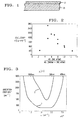
    • FIG. 1 is a schematic cross section of a substrate coated with conductively doped zinc-indium-oxide; and
    • FIG. 2 is a diagram showing the conductivity of several different tin-doped zinc-indium-oxide films deposited by pulsed laser deposition and dc magnetron sputter deposition.
    • FIG. 3 is a graphical display of absorption versus wavelength for conductively doped zinc-indium-oxide in comparison with conventional indium tin oxide (ITO).
    • FIG. 4 shows the use of conductively doped zinc-indium-oxide electrodes in a liquid crystal display device.
    Detailed Description
  • Applicants have discovered a composition of matter comprising zinc-indium-oxide wherein indium is 40-75 atomic % of the metal elements. The composition is useful as a transparent conductive material, especially in devices comprising a layer of the material disposed on a substrate such as a transparent substrate of glass, plastic or semiconductor. The material is advantageously doped with an aliovalent material having a valence different from either zinc (+2) or indium (+3). Preferably the doping material is a tetravalent material. Compositions and devices employing the new material can be advantageously aliovalently doped to resistivities less than 1 milliohm-cm. It is possible to substitute a material M having a valence greater than 3 for the indium to produce Znx(In2-yMy)z oxide where 2z is 40-75 atomic % of the metal elements and 0.005 ≤ y ≤ 0.4. It is also possible to substitute a material M having a valence greater than 2 for the zinc to produce Zn1-w Mw Iny oxide where y is 40-75 atomic % of the metal elements and 0.005 ≤ w ≤ 0.4. In addition, one can simultaneously substitute for Zn a material M having a valence greater than 2 and for In a material M' having a valence greater than 3 to produce Znx-wMw(In2-yM ' y
    Figure imgb0001
    ) oxide where 2/(x+2) is 40-75 atomic % of the metal elements. In a series of experiments using zinc-indium-oxide ceramic samples prepared as described below, it was determined that films prepared from ceramic targets with composition Zn2.5 In 2-x Snx Oy with 0.1 ≤ x ≤ 0. 3 had optimal properties. It was further determined that a target of Zn2.5 In 1.7 Sn.3 Oy yielded a film 0.5 micrometer thick with composition Zn1.4 In1.7 Sn.3 Oy. Methods for preparing conductively doped zinc-indium-oxide can be understood by consideration of the following examples.
  • Example 1
  • Powdered zinc oxide, ZnO, indium oxide, In₂O₃, and tin oxide, SnO₂, are weighed out to yield the appropriate mole ratios for Zn2.5 In 2-x Snx Oy, O ≤ x ≤ 0.3. For instance, for a 5-gram total weight sample of Zn2.5 In1.7 Sn₃ Oy, 2.0899 grams of ZnO, 2.4348 grams of In₂O₃ and 0.4664 grams of SnO₂ are used. The powders are mixed together and ground together in a mechanical mortar and pestle for a minimum of five minutes to insure good mixing and contact of powder particles. The mixed powders are transferred into high density aluminum oxide crucibles with cover and heated in air for an initial period of 12-15 hours at 1100 °C. The resulting powders are then ground mechanically again, re-introduced into the covered aluminum oxide crucibles, and heated for a period of 12-15 hours at 1200°C in air. After a third grinding, pellets are pressed in a standard steel dye (typically to a load of 3000 pounds for a half-inch diameter pellet). The pellets are then heated at 1300°C in air for a period of up to 16 hours. Pellets are typically buried in powder of their own composition inside the covered aluminum oxide crucibles for the pellet firing step. The pellets are cooled after this heating step at the natural cooling rate of the furnace, which in our case results in reaching 300°C in approximately three hours, at which point the pellets are removed from the furnace. Air is selected as an ambient for the initial processing steps because of its convenience. Covers are placed over the crucibles as a precaution to prevent evaporation of the oxides, but we have not observed evaporation under the conditions described. The times of these treatments are expected to be dependent on the reactivities of the starting materials and the efficiencies of the grinding operations. Shorter times can be expected to give equally satisfactory results, for example, in the preparation of ceramic targets for sputtering or laser ablation.
  • The bulk material after air firing is not in its optimally conducting state. A further treatment is advantageous to improve the conductivity. In this treatment, a heating of duration 10-12 hours in flowing N₂ (approximately 100 cc/min, N₂ typically approximately 50-100 ppm O₂) in a ceramic tube furnace at 1200°C is employed, again with the pellets allowed to cool at the natural furnace cooling rate. Covered aluminum oxide crucibles and a powder bed for the pellets need not necessarily be employed for this step. The pellets emerge from the N₂ treatment with good electrical conductivity.
  • Example 2
  • Processing conditions are as described in Example 1 except that after firing in air the pellets are heated in a nitrogen-hydrogen (15 mole percent hydrogen) ambient rather than in N ₂, and at a temperature of 400°C rather than 1200°C, for a period of one hour.
  • Example 3
  • Processing conditions as described in Examples 1 and 2, with ZnO, Al₂O₃, and In₂O₃ in appropriate mole ratios to yield Zn2.5-x Alx In₂Oy. For example for Zn2.3 Al.2 In₂ Oy in an 8 gram batch, 3.1521 grams of ZnO, 0.1717 grams of Al₂O₃ and 4.6762 grams of In₂O₃ are employed.
  • Example 4
  • Processing conditions as described in Examples 1 and 2, with ZnO, Ga₂O₃ and In₂O₃ mixed in appropriate mole ratios to yield Zn2.5-x Gax In₂Oy. For example for Zn2.3 Ga.2 In₂Oy in an 8 gram batch, 3.0964 grams of ZnO, 0.3101 grams of Ga₂O₃ and 4.5935 grams of In₂O₃ are employed.
  • Example 5
  • Processing as described in examples 1 and 2 with ZnO, GeO₂ and In₂O₃ mixed in the appropriate mole ratios to yield Zn2.5-x Gex In₂Oy. For example for Zn2.3 Ge.2 In₂Oy in an 8 gram batch, 3.0825 grams of ZnO, 0.3445 grams of GeO₂, and 4.5729 grams of In₂O₃ are employed.
  • It is contemplated that a basic use of zinc-indium-oxide is to provide transparent coatings on substrates such as glass, semiconductor or plastic. For example, the ability of the material to transmit light of any wavelength from 0.45µm to 1.5µm makes it useful as a coating material for windows, solar cells or display devices. Such coated substrates permit selective entry of visible and infrared light while reflecting ultraviolet. FIG. 1 is a schematic cross section of a substrate 30, such as a transparent glass, coated with a thin layer 31 comprising conductively doped zinc-indium-oxide. Preferably the coating is in the form of a thin continuous amorphous or polycrystalline layer having a thickness typically in the range 0.1µm to 1 µm. The method for coating a substrate 30 can be understood by considering the following examples.
  • Example 6 (Deposition By Laser Ablation)
  • A pressed pellet of Zn2.5 In1.7 Sn.3 Ox was placed in the target holder of a pulsed laser deposition vacuum chamber and a vitreous quartz substrate was mounted onto a heatable substrate holder facing the target and positioned about 8 cm from the target. The chamber was evacuated to a base pressure of 1-10x10⁻⁷ Torr and 1 m Torr of oxygen was bled into the chamber. The substrate was heated to 250°C, and then the target was bombarded by pulses from a KrF excimer laser operating at 248 nm with a pulse repetition rate at 10 Hz. The energy density of the laser on target was 1-4 J/cm. The deposition rate was 1000-2000 angstroms per hour. After growth of several thousand angstroms, the chamber was again evacuated and the substrate was permitted to cool to room temperature. The films subsequently removed from the chamber were transparent to the eye with good electrical conductivity, i.e., resistivity as low as 500 µΩ-cm. Film composition as determined by Rutherford backscattering was Zn0.7(In1.7 Sn.3)0.5Oy. FIG. 2 is a diagram showing conductivities of several different tin doped zinc-indium-oxide films deposited by pulsed laser deposition and by sputtering. In the figure the abcissa is the ratio in the film of zinc content to (In+Sn) content.
  • Example 7 (Deposition By Sputtering)
  • A pressed pellet of zinc-indium-oxide doped with tin Zn2.5 In1.7 Sn0.3 Ox was placed in the target holder of a dc magnetron sputter deposition chamber. Corning glass and vitreous quartz substrates were placed in proximity to the target in two configurations: (1) on-axis geometry directly underneath the target and (2) off-axis geometry outside the plasma plume, approximately 0.5-2.0 cm from the edge of the sputtering gun. The chamber was evacuated, and a sputtering gas consisting of an argon-oxygen mixture (15-1 ratio) at 4-20 m Torr was introduced. The substrate was heated to 250°C - 500°C. The film composition was Zn₁ In1.7 Sn0.3 Ox at 350°C and Zn1.2 In1.7 Sn0.3 Ox at 450°C. The target was then impacted by the sputter gun (a US 1" magnetron source) operating at a dc voltage of 350V, a current of 0.78A, and a power level of 25 Watts. The growth rate was about 1.3 µm per hour in the on-axis geometry and .25 to 0.5 µm per hour in the off-axis geometry. Film resistivity as low as 380 µΩ-cm was obtained for a film deposited at 450°C.
  • FIG. 3 is a graphical illustration of the absorption spectrum of conductively doped zinc-indium-oxide (curve 1) in comparison with that of conventional ITO (curve 2). As can be seen, the zinc-indium-oxide film exhibits uniformly small absorption across the visible spectrum (from about 400 to 700 nm).
  • One important use of zinc-indium-oxide coated substrates is in flat panel display devices using transparent electrodes such as liquid crystal displays. Electrodes comprising zinc-indium-oxide can provide enhanced transparency, particularly in the visible blue region. FIG. 4, which is a schematic rendering of a portion of an active matrix liquid crystal display device (AMLCD), shows how the product of FIG. 1 can be used to make an improved flat panel display. In essence the AMLCD comprises a liquid crystal medium (not shown) disposed between a transparent common electrode 50 and an array of transistors 51 and a local electrodes 52 (preferably pixel-size) disposed on a common substrate 30. Each local electrode is switched by an associated transistor 51 interconnected to an associated storage capacitor 53. The transistors 51 thereby control the state of the voltage on each local electrode 52 and, in accordance with well known principles, control the optical state of a pixel-size liquid crystal region.
  • In accordance with conventional structure, the AMLCD includes a back light (not shown), a diffuser 54, polarizers 55 and a grid of color filter layers 56 disposed on a transparent substrate 59. Rows of transistor gates can be interconnected via conductive gate lines 57 and columns of transistor sources can be interconnected via conductive data lines 58 for switchable control of individual pixels.
  • The AMLCD of FIG. 4 is of conventional construction except that the transparent electrodes comprise zinc-indium-oxide coated on glass substrates as shown in FIG. 1. The material is preferably conductively doped with an aliovalent dopant. The advantage of using the inventive transparent conducting material in this AMLCD include greater conductivity, enhanced transparency and more realistic color display, especially in the blue portion of the visible spectrum. While zinc-indium-oxide is the preferred composition for the transparent electrodes, any of the new conductively doped compositions disclosed herein can be used with similar advantages. Moreover, while liquid crystal displays have been described, the conductively doped compositions can be used as transparent electrodes on other types of flat panel displays such as electron emission displays.

Claims (19)

  1. A transparent conductive material comprising zinc-indium-oxide wherein indium is 40-75 atomic % of the metal elements.
  2. The transparent conductive material of claim 1 doped with an aliovalent material.
  3. The transparent conductive material of claim 2 wherein said aliovalent material is a tetravalent material.
  4. The composition of matter comprising zinc-indium-oxide doped with an aliovalent material to a resistivity less than 1 milliohm-cm.
  5. The composition of claim 4 wherein said aliovalent material is a tetravalent material.
  6. The composition of matter comprising Znx(In2-yMy)z oxide where M is a material with a valence greater than 3, 2z is 40-75 atomic % of the metal elements and 0.005 ≤ y ≤ 0.4.
  7. The composition of claim 6 wherein M is a tetravalent material.
  8. The composition of claim 7 where M is Sn.
  9. The composition of matter comprising Zn1-w MwIny oxide where M is a material having a valence greater than 2, where y is 40-75 atomic % of the metal elements and 0.005 ≤ w ≤ 0.4.
  10. The composition of claim 9 where M is Al, Ga or Ge.
  11. The composition of matter comprising Znx-wMw(In2-yM ' y
    Figure imgb0002
    ) oxide where M is a material having a valence greater than 2 and M' is a material having a valence greater than 3 and wherein 2 x+2
    Figure imgb0003
    is 40-75 %.
  12. A device comprising a substrate and disposed thereon a transparent conductive material comprising zinc-indium-oxide containing 40-75 atomic % In.
  13. A device according to claim 12 wherein said substrate is transparent.
  14. A device according to claim 12 wherein said substrate comprises glass, plastic or a semiconductor.
  15. A device according to claim 12 wherein said zinc-indium-oxide is doped with a tetravalent material.
  16. A device comprising a substrate and disposed thereon a transparent conductive material comprising the composition of claim 6 or 7 or 8 or 9 or 10 or 11.
  17. In a liquid crystal display device comprising a pair of electrodes, a liquid crystal medium disposed between said electrodes and means for applying a voltage between said electrodes, the improvement wherein:
       at least one of said electrodes comprises a transparent, conductive layer comprising zinc-indium-oxide where indium is 40-75 atomic % of the metal elements.
  18. The improved liquid crystal display of claim 17 wherein said zinc-indium-oxide is doped with an aliovalent material.
  19. A flat panel display device comprising a pair of electrodes and means for applying a voltage between said electrodes, wherein said transparent electrode comprises the composition of claim 6 or 7 or 8 or 9 or 10 or 11.
EP95307028A 1994-10-13 1995-10-03 Transparent conductors comprising zinc-indium-oxide and methods for making films Withdrawn EP0707320A1 (en)

Applications Claiming Priority (4)

Application Number Priority Date Filing Date Title
US335615 1981-12-30
US32290294A 1994-10-13 1994-10-13
US322902 1994-10-13
US33561594A 1994-11-08 1994-11-08

Publications (1)

Publication Number Publication Date
EP0707320A1 true EP0707320A1 (en) 1996-04-17

Family

ID=26983669

Family Applications (1)

Application Number Title Priority Date Filing Date
EP95307028A Withdrawn EP0707320A1 (en) 1994-10-13 1995-10-03 Transparent conductors comprising zinc-indium-oxide and methods for making films

Country Status (2)

Country Link
US (1) US5628933A (en)
EP (1) EP0707320A1 (en)

Cited By (2)

* Cited by examiner, † Cited by third party
Publication number Priority date Publication date Assignee Title
DE29711973U1 (en) * 1997-07-08 1998-11-05 Glas Platz Fa Electrical device, electrical device or lighting device
US6221520B1 (en) 1996-07-26 2001-04-24 Asahi Glass Company Ltd. Transparent conductive film and process for forming a transparent electrode

Families Citing this family (10)

* Cited by examiner, † Cited by third party
Publication number Priority date Publication date Assignee Title
JP4837811B2 (en) * 1998-04-09 2011-12-14 出光興産株式会社 Organic electroluminescence device
US6480633B1 (en) * 1999-06-17 2002-11-12 Agere Systems Inc. Electro-optic device including a buffer layer of transparent conductive material
JP2001306258A (en) * 2000-02-18 2001-11-02 Nippon Sheet Glass Co Ltd Substrate with transparent conductive film for touch panel
KR100776505B1 (en) * 2000-12-30 2007-11-16 엘지.필립스 엘시디 주식회사 Fabricating Method of Pixel Pole in the Liquid Crystal Display
US6645843B2 (en) * 2001-01-19 2003-11-11 The United States Of America As Represented By The Secretary Of The Navy Pulsed laser deposition of transparent conducting thin films on flexible substrates
US6748264B2 (en) 2002-02-04 2004-06-08 Fook Tin Technologies Limited Body fat analyzer with integral analog measurement electrodes
US7300617B2 (en) * 2004-05-13 2007-11-27 David Gerling Method of making fusion cast articles
US8197908B2 (en) * 2008-03-14 2012-06-12 Hestia Tec, Llc Method for preparing electrically conducting materials
KR101153900B1 (en) 2009-08-27 2012-06-18 한국세라믹기술원 Power factor improved Zinc-Indium oxide composition and the manufacturing method of sintered body of the same
US9927667B2 (en) 2014-08-11 2018-03-27 Sci Engineered Materials, Inc. Display having a transparent conductive oxide layer comprising metal doped zinc oxide applied by sputtering

Citations (4)

* Cited by examiner, † Cited by third party
Publication number Priority date Publication date Assignee Title
JPH06187832A (en) * 1992-12-15 1994-07-08 Idemitsu Kosan Co Ltd Manufacture of transparent conductive film
JPH06234522A (en) * 1992-12-16 1994-08-23 Idemitsu Kosan Co Ltd Electrically conductive material and its production
JPH07235219A (en) * 1993-12-28 1995-09-05 Idemitsu Kosan Co Ltd Conductive transparent substrate and its manufacture
EP0677593A1 (en) * 1992-12-15 1995-10-18 Idemitsu Kosan Company Limited Transparent conductive film, transparent conductive base material, and conductive material

Family Cites Families (6)

* Cited by examiner, † Cited by third party
Publication number Priority date Publication date Assignee Title
US4172922A (en) * 1977-08-18 1979-10-30 Trw, Inc. Resistor material, resistor made therefrom and method of making the same
JPS56143443A (en) * 1980-04-11 1981-11-09 Fuji Photo Film Co Ltd Electrically conductive support for electrophotographic material
DE3566184D1 (en) * 1984-06-22 1988-12-15 Hitachi Ltd Oxide resistor
US4990286A (en) * 1989-03-17 1991-02-05 President And Fellows Of Harvard College Zinc oxyfluoride transparent conductor
US5196102A (en) * 1991-08-08 1993-03-23 Microelectronics And Computer Technology Corporation Method and apparatus for applying a compound of a metal and a gas onto a surface
JP3834339B2 (en) * 1992-12-15 2006-10-18 出光興産株式会社 Transparent conductive film and method for producing the same

Patent Citations (4)

* Cited by examiner, † Cited by third party
Publication number Priority date Publication date Assignee Title
JPH06187832A (en) * 1992-12-15 1994-07-08 Idemitsu Kosan Co Ltd Manufacture of transparent conductive film
EP0677593A1 (en) * 1992-12-15 1995-10-18 Idemitsu Kosan Company Limited Transparent conductive film, transparent conductive base material, and conductive material
JPH06234522A (en) * 1992-12-16 1994-08-23 Idemitsu Kosan Co Ltd Electrically conductive material and its production
JPH07235219A (en) * 1993-12-28 1995-09-05 Idemitsu Kosan Co Ltd Conductive transparent substrate and its manufacture

Non-Patent Citations (4)

* Cited by examiner, † Cited by third party
Title
DATABASE CHEMABS CHEMICAL ABSTRACTS SERVICE, COLUMBUS, OHIO, US; OOYAMA, MASATSUGU ET AL: "Electroconductive transparent substrates and their manufacture" *
DATABASE CHEMABS CHEMICAL ABSTRACTS SERVICE, COLUMBUS, OHIO, US; UMIGAMI, AKIRA ET AL: "Manufacture of transparent electric conductive films" *
MINAMI, TADATSUGU ET AL: "Highly transparent and conductive Zn2In2O5 thin films prepared by RF magnetron sputtering", JPN. J. APPL. PHYS., PART 2 (1995), 34(8A), L971-L974 CODEN: JAPLD8;ISSN: 0021-4922 *
PATENT ABSTRACTS OF JAPAN vol. 018, no. 610 (C - 1276) 21 November 1994 (1994-11-21) *

Cited By (3)

* Cited by examiner, † Cited by third party
Publication number Priority date Publication date Assignee Title
US6221520B1 (en) 1996-07-26 2001-04-24 Asahi Glass Company Ltd. Transparent conductive film and process for forming a transparent electrode
US6465117B2 (en) 1996-07-26 2002-10-15 Asahi Glass Company Ltd. Transparent conductive film and process for forming a transparent electrode
DE29711973U1 (en) * 1997-07-08 1998-11-05 Glas Platz Fa Electrical device, electrical device or lighting device

Also Published As

Publication number Publication date
US5628933A (en) 1997-05-13

Similar Documents

Publication Publication Date Title
EP0651399B1 (en) Transparent conductors comprising gallium-indium-oxide
US5397920A (en) Light transmissive, electrically-conductive, oxide film and methods of production
Nagatomo et al. Electrical and optical properties of vacuum-evaporated indium-tin oxide films with high electron mobility
Phillips et al. Zinc‐indium‐oxide: a high conductivity transparent conducting oxide
Mizuhashi Electrical properties of vacuum-deposited indium oxide and indium tin oxide films
Nath et al. Preparation of In2O3 and tin-doped In2O3 films by a novel activated reactive evaporation technique
Haacke Transparent electrode properties of cadmium stannate
US7858206B2 (en) Transparent conductor, transparent electrode, solar cell, light emitting device and display panel
US6761986B2 (en) Thin film infrared transparent conductor
EP2128876B1 (en) Process for producing electroconductor
US4349425A (en) Transparent conductive films and methods of producing same
US5628933A (en) Transparent conductors comprising zinc-indium-oxide and methods for making films
Ma et al. Preparation and properties of transparent conducting indium tin oxide films deposited by reactive evaporation
JP2000067657A (en) Transparent conductive film excellent in infrared transmission and its manufacture
WO2002031215A2 (en) Method of forming indium tin oxide film
JP3644647B2 (en) Conductive oxide and electrode using the same
Farahamndjou The study of electro-optical properties of nanocomposite ITO thin films prepared by e-beam evaporation
Dutta et al. Variations in structural and electrical properties of magnetron-sputtered indium tin oxide films with deposition parameters
US5652062A (en) Devices using transparent conductive GaInO3 films
US5473456A (en) Method for growing transparent conductive gallium-indium-oxide films by sputtering
Lloyd Properties of cadmium stannate films prepared by rf sputtering from powder targets
Fujinaka et al. Tin-doped In2O3 films deposited by RF sputtering
JPH08227614A (en) Transparent conductor containing zinc-indium oxide and manufacture of thin-film
CA2156557A1 (en) Transparent conductors comprising zinc-indium-oxide and methods for making films
JP2001133814A (en) Self-power supply type dimming element

Legal Events

Date Code Title Description
PUAI Public reference made under article 153(3) epc to a published international application that has entered the european phase

Free format text: ORIGINAL CODE: 0009012

AK Designated contracting states

Kind code of ref document: A1

Designated state(s): DE FR GB NL

STAA Information on the status of an ep patent application or granted ep patent

Free format text: STATUS: THE APPLICATION HAS BEEN WITHDRAWN

18W Application withdrawn

Withdrawal date: 19960416