EP0709741A1 - Photolithographic process for circular dense patterns - Google Patents
Photolithographic process for circular dense patterns Download PDFInfo
- Publication number
- EP0709741A1 EP0709741A1 EP95410118A EP95410118A EP0709741A1 EP 0709741 A1 EP0709741 A1 EP 0709741A1 EP 95410118 A EP95410118 A EP 95410118A EP 95410118 A EP95410118 A EP 95410118A EP 0709741 A1 EP0709741 A1 EP 0709741A1
- Authority
- EP
- European Patent Office
- Prior art keywords
- layer
- microbeads
- photolithography
- circular patterns
- resin
- Prior art date
- Legal status (The legal status is an assumption and is not a legal conclusion. Google has not performed a legal analysis and makes no representation as to the accuracy of the status listed.)
- Granted
Links
Images

Classifications
-
- G—PHYSICS
- G03—PHOTOGRAPHY; CINEMATOGRAPHY; ANALOGOUS TECHNIQUES USING WAVES OTHER THAN OPTICAL WAVES; ELECTROGRAPHY; HOLOGRAPHY
- G03F—PHOTOMECHANICAL PRODUCTION OF TEXTURED OR PATTERNED SURFACES, e.g. FOR PRINTING, FOR PROCESSING OF SEMICONDUCTOR DEVICES; MATERIALS THEREFOR; ORIGINALS THEREFOR; APPARATUS SPECIALLY ADAPTED THEREFOR
- G03F7/00—Photomechanical, e.g. photolithographic, production of textured or patterned surfaces, e.g. printing surfaces; Materials therefor, e.g. comprising photoresists; Apparatus specially adapted therefor
- G03F7/20—Exposure; Apparatus therefor
-
- G—PHYSICS
- G03—PHOTOGRAPHY; CINEMATOGRAPHY; ANALOGOUS TECHNIQUES USING WAVES OTHER THAN OPTICAL WAVES; ELECTROGRAPHY; HOLOGRAPHY
- G03F—PHOTOMECHANICAL PRODUCTION OF TEXTURED OR PATTERNED SURFACES, e.g. FOR PRINTING, FOR PROCESSING OF SEMICONDUCTOR DEVICES; MATERIALS THEREFOR; ORIGINALS THEREFOR; APPARATUS SPECIALLY ADAPTED THEREFOR
- G03F7/00—Photomechanical, e.g. photolithographic, production of textured or patterned surfaces, e.g. printing surfaces; Materials therefor, e.g. comprising photoresists; Apparatus specially adapted therefor
- G03F7/0015—Production of aperture devices, microporous systems or stamps
-
- G—PHYSICS
- G03—PHOTOGRAPHY; CINEMATOGRAPHY; ANALOGOUS TECHNIQUES USING WAVES OTHER THAN OPTICAL WAVES; ELECTROGRAPHY; HOLOGRAPHY
- G03F—PHOTOMECHANICAL PRODUCTION OF TEXTURED OR PATTERNED SURFACES, e.g. FOR PRINTING, FOR PROCESSING OF SEMICONDUCTOR DEVICES; MATERIALS THEREFOR; ORIGINALS THEREFOR; APPARATUS SPECIALLY ADAPTED THEREFOR
- G03F7/00—Photomechanical, e.g. photolithographic, production of textured or patterned surfaces, e.g. printing surfaces; Materials therefor, e.g. comprising photoresists; Apparatus specially adapted therefor
- G03F7/20—Exposure; Apparatus therefor
- G03F7/2002—Exposure; Apparatus therefor with visible light or UV light, through an original having an opaque pattern on a transparent support, e.g. film printing, projection printing; by reflection of visible or UV light from an original such as a printed image
- G03F7/2014—Contact or film exposure of light sensitive plates such as lithographic plates or circuit boards, e.g. in a vacuum frame
- G03F7/2016—Contact mask being integral part of the photosensitive element and subject to destructive removal during post-exposure processing
-
- H—ELECTRICITY
- H01—ELECTRIC ELEMENTS
- H01J—ELECTRIC DISCHARGE TUBES OR DISCHARGE LAMPS
- H01J9/00—Apparatus or processes specially adapted for the manufacture, installation, removal, maintenance of electric discharge tubes, discharge lamps, or parts thereof; Recovery of material from discharge tubes or lamps
- H01J9/02—Manufacture of electrodes or electrode systems
- H01J9/022—Manufacture of electrodes or electrode systems of cold cathodes
- H01J9/025—Manufacture of electrodes or electrode systems of cold cathodes of field emission cathodes
Definitions
- the present invention relates to a process for photolithography of circular patterns. It applies more particularly to a process of photolithography of circular patterns of small diameter in a layer to be etched which must have a high density of patterns.
- photolithography of circular patterns consists in depositing a layer of photosensitive product commonly called resin on the layer to be etched, to insolate this layer of resin by means of a mask, and to etch.
- This technique is no longer applicable or becomes excessively expensive when it is desired to produce patterns of very small diameter at high density on large surface layers.
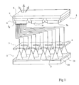
- Figure 1 shows the structure of a microtip flat screen.
- a microtip screen is essentially consisting of a cathode 1 with microtips 2 and a grid 3 provided with holes 4 corresponding to the locations of the microtips 2.
- the cathode 1 is placed opposite a cathodoluminescent anode 5 of which a glass substrate 6 constitutes the surface of screen.
- the cathode 1 is organized in columns and consists, on a glass substrate 10, of cathode conductors organized in meshes from a conductive layer.
- the microtips 2 are produced on a resistive layer 11 deposited on the cathode conductors and are arranged inside the meshes defined by the cathode conductors.
- FIG. 1 partially represents the interior of a mesh, the cathode conductors do not appear in this figure.
- the cathode 1 is associated with the grid 3 which is organized in lines. The intersection of a line of the grid 3 and a column of the cathode 1 defines a pixel.
- This device uses the electric field created between the anode 5 and the cathode 1 so that electrons are extracted from the microtips 2 towards a cathodoluminescent layer 7 of the anode 5, under the control of the grid 3.
- the anode 5 is provided with alternating bands of phosphor elements 7, each corresponding to a color (Blue, Red, Green). The strips are separated from each other by an insulator 8.
- the phosphor elements 7 are deposited on electrodes 9, consisting of corresponding strips of a transparent conductive layer such as indium tin oxide (ITO) .
- ITO indium tin oxide
- the sets of blue, red and green bands are alternately polarized with respect to the cathode 1 so that the electrons extracted from the microtips 2 of a pixel of the cathode / grid are alternately directed towards the phosphor elements 7 opposite each of the colors.
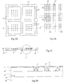
- FIGS. 2A to 2D illustrate an example of a constitution of this type, FIGS. 2B and 2D being respectively enlargements of parts of FIGS. 2A and 2C.
- Several microtips 2, for example sixteen, are arranged in each mesh 12 defined by the cathode conductors 13 (FIG. 2B).
- the intersection of a line 14 of the grid 3 and a column 15 of the cathode 1 corresponds here, for example, to sixty-four meshes 12 of a cathode pixel (FIG. 2A).
- the cathode 1 generally consists of layers deposited successively on the glass substrate 10.
- FIGS. 2C and 2D partially show a sectional view along the line A-A 'of FIG. 2B.
- a conductive layer 13, for example made of niobium, is deposited on the substrate 10. This layer 13 is etched in a pattern of columns 15, each column having meshes 12 surrounded by cathode conductors 13.
- a resistive layer 11 is then deposited on these cathode conductors 13.
- the purpose of this resistive layer 11, made for example of amorphous silicon doped with phosphorus, is to protect each microtip 2 against an excess of current at the start of a microtip 2.
- the affixing of such a resistive layer 11 aims to homogenize the electronic emission of the microtips 2 of a pixel of the cathode 1 and thus to increase its lifetime.
- the grid 3 is formed of a conductive layer, for example of niobium.
- Holes 4 and wells 17 are respectively made in layers 3 and 16 to receive the microtips 2 which are for example made of molybdenum.
- the production of the cathode 1 with microtips 2 therefore requires the formation of circular holes 4 and cylindrical wells 17 in the grid 3 and in the insulating layer 16.
- the formation of these holes 4 and wells 17 calls for a method of photolithography of circular patterns.
- a photosensitive resin is applied to the grid layer 3 which is exposed to the sun after being partially masked to determine the position of the holes 4 and therefore of the microtips 2.
- the diameter of a well 17 has a value between 1 and 2 ⁇ m, the pitch being of the order of 2 to 10 ⁇ m, and the number of microtips is several thousand per screen pixel.
- the object of the present invention is to overcome the drawbacks of current techniques by proposing a process for photolithography of circular patterns which makes it possible to obtain a regular diameter of the circular patterns and a regular density of patterns, regardless of the surface of the layer to be engrave.
- the present invention provides a process for photolithography of dense circular patterns of small diameter in a layer, consisting in depositing a layer of resin on said layer and in exposing this layer of resin, a process which consists in carrying out, beforehand at a sunshine step, a deposit of calibrated microbeads, opaque for sunshine radiation, on the surface of the resin layer.
- the microbeads have a given diameter of between 1 and 5 ⁇ m.
- the insolation step is carried out by means of a quasi-parallel beam of ultraviolet radiation.
- the step of depositing the microbeads consists in spraying, on the resin layer, an alcohol-based solvent with which the microbeads have been previously mixed.
- the step of depositing the microbeads consists in drowning the resin layer in a bath containing microbeads in suspension, and in allowing the microbeads to settle on the resin layer by gravity.
- the insolation step is carried out by means of a beam insulator almost parallel to a given axis; and the resin layer is arranged at a predetermined angle relative to this axis around which it is rotated.
- the method consists in carrying out, prior to the step of depositing the microbeads, a step of pre-insulating the resin layer, by masking predetermined surfaces in which the circular patterns must be engraved.
- the invention also provides for the application of such a method of photolithography of circular patterns, for the manufacture of a cathode of a microtip screen, the resin layer being applied to a stack of layers comprising successively from a substrate, a layer of cathode conductors organized in columns provided with meshes, a resistive layer, an insulation layer and a grid conductive layer; the circular patterns defining in the grid and isolation layers, locations of holes and wells for receiving the microtips.
- a step of pre-exposure of the resin layer is carried out, prior to the step of depositing the microbeads, by masking surfaces at most equivalent to the meshes defined by the cathode conductors.
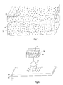
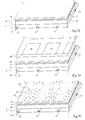
- a layer of photosensitive resin 18 of negative type is applied to a layer 19 to be etched.
- microbeads 20 are deposited on the resin layer 18.
- These microbeads 20 are for example microbeads of glass or plastic. They are opaque to sunshine to obtain a maximum masking effect on the areas on which they are deposited.
- the distribution of the microbeads 20 on the resin layer 18 is random. The invention therefore applies more particularly to a method of photolithography of circular patterns for which an essentially regularity is sought in the diameter of the patterns and in the density of the patterns throughout the layer.
- microbeads 20 of small diameter regular from one microbead to another, for example at a given value between 1 and 2 ⁇ m are used better than 10 % near.
- microbeads 20 are random. It is however important to ensure that the density of the microbeads 20 deposited on the layer 18 is sufficient and regular. To do this, it is possible to use, according to the invention, several methods of depositing microbeads 20, which will be described later in relation to FIGS. 5 and 6.
- this resin layer 18 is exposed by means of an insolator 21 with quasi-parallel light during a third step (FIG. 3C).
- the wavelength of the radiation from the insolator 21 is chosen as a function of the resin used and the precision sought, for example in the ultraviolet range.
- the microbeads 20 are then removed from the resin layer 18 during a fourth step (not shown).
- a fifth step (FIG. 3D) the resin is developed by the implementation of a conventional process under conditions compatible with the type of resin used. Circular patterns 22 are thus formed in the resin layer 18 at the locations of the microbeads 20, and are then used to engrave corresponding patterns in layer 19.
- FIGS. 4A and 4B A variant of the insolation step (third step) is shown in FIGS. 4A and 4B.
- This variant consists in exposing the resin layer 18, still by means of an insulator 21 with quasi-parallel light, but by tilting the layer 18 relative to the axis Y of the beam, and by rotating it around this axis. Y.
- the etching layer 19, coated with the resin layer 18 on which the microbeads 20 have been deposited is placed for example on a rotary support 23 inclined by a given angle ⁇ relative to the axis. Y of the beam.
- the diameter d actually insulated directly above each microbead 20 is less than the diameter of the microbeads 20.
- the ratio between the diameter of the microbeads 20 and the diameter d of the patterns 22 obtained depends on the angle of inclination ⁇ of the support 23 relative to the axis Y of the quasi-parallel beam of radiation from the insulator 21.
- This variant further improves the resolution obtained by implementing the method according to the invention. It is indeed possible to use microbeads 20 of larger size which will have better uniformity between them. It is possible, for example, to produce patterns 22 of diameter 2 ⁇ m by means of microbeads 20 having a diameter of 5 ⁇ m.
- a first method (FIG. 5) consists in immersing the etching layer 19, coated with the resin layer 18, in a bath 24 containing microbeads 20 in suspension.
- the density of the microbeads 20 in the bath is fixed as a function of the density of patterns 22 desired.
- the deposit of microbeads 20 is carried out by decantation, the microbeads used in this case being made of glass. It is also possible to carry out the insolation step through the bath 24 as soon as the microbeads 20 have decanted, which accelerates the execution of the process.
- the evacuation of the microbeads 20, after exposure, is carried out here simply by removing the layer to be etched 19 and its possible support from the bath 24.
- a second method (FIG. 6) consists in spraying, on the resin layer 18, a mixture of solvent 25 and microbeads 20 contained in a tank 26.
- the solvent 25 is alcohol-based, which allows its evaporation during the spray.
- the distribution of the microbeads 20 on the resin layer 18 has good homogeneity, the density of microbeads 20 being fixed by the duration of the spraying carried out.
- the microbeads 20 hold on the resin layer 18 by electrostatic effect, resulting from charges acquired during their passage of air between a nozzle 27 of the sprayer and the resin layer 18.
- the evacuation of the microbeads 20 after insolation can be performed by blowing or any other means.
- Another variant (not shown) of the invention consists in embedding microbeads 20 in a viscous material, for example polyvinyl alcohol.
- a viscous material for example polyvinyl alcohol.
- the resin layer 18 is covered with a layer of this material, for example by scraping or by screen printing without a pattern.
- the polyvinyl alcohol is then dried and then exposed as described above. Subsequently, the polyvinyl alcohol is dissolved, for example in water, and the microbeads 20 are removed at the same time.
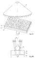
- FIGS. 7A to 7C illustrate an example of application of the method described above to the production of circular patterns defining the locations of the microtips in a microtip cathode of a flat display screen.
- FIG. 7A represents the stack of layers that a cathode 1 with microtips comprises prior to the implementation of the photolithography method according to the invention.
- a conductive layer for example based on niobium, is deposited on a substrate 10. This conductive layer is etched to define cathode conductors 13. These conductors 13 are organized in columns provided with meshes 12, each mesh 12 defining a microtip reception area 2, and each column having a width corresponding to that of a screen pixel.
- a resistive layer 11 is then deposited on the cathode conductors 13.
- an insulating layer 16 is deposited, for example made of silicon oxide (SiO2), which isolates the cathode conductors 13 from a grid layer 3, by example based on niobium, which ends the stack.
- the layer 19 to be etched by the implementation of the method according to the invention here consists of the two grid 3 and insulation 16 layers in which it is desired to form holes 4 and cylindrical wells 17 for receiving the microtips 2.
- the use of the photolithography process according to the invention is made possible by the fact that it has been observed that the quality of a screen was linked to the regularity of the density of the microtips 2 of a pixel of the screen. to another and to the regularity of the diameter of the microtips 2.
- the difference between two microtips 2 has no influence on the quality of the screen provided that the density of microtips is high.
- the random distribution of the patterns 22 in the layer 19 has no consequence on the quality of the screen. It was thus found that a good quality flat screen was obtained with a number and a diameter of circular patterns 22 in each pixel of the screen which are the same to the nearest five percent, the density of patterns 22 of a pixel being high so as not to affect the brightness of the screen.
- a deposit of 20 calibrated microbeads of a given diameter with a value between 1 and 5 ⁇ m with a tolerance of 10 percent for the diameter of the microbeads 20 achieves this result.
- This variant consists in carrying out a double exposure of the resin layer 18 by carrying out a pre-exposure step before the step of depositing the microbeads 20.
- the resin layer 18 is pre-insulated through a conventional mask 28 for closing the surfaces 29 contained in the meshes 12 defined by the cathode conductors 13.
- a conventional mask 28 is here satisfactory insofar as the intervals between the groups of microtips 2 represent a sufficient distance (of the order of 10 to 20 ⁇ m) for the resolutions of this type of mask, the meshes 12 being devoid of microtips 2 at their periphery. In addition, this distance makes it possible to accept a certain tolerance in the mask 28. Then the execution of the process as described using FIGS. 3B to 3D is resumed.
- FIGS. 3B to 3D is resumed.
- the microbeads 20 are deposited by any of the methods set out above in relation to FIGS. 5 and 6.
- the exposure from the third step (FIG. 3C or 4A) is then carried out. This exposure is only effective in the surfaces 29 which were masked during the intermediate pre-exposure step, ie towards the center of the meshes 12.
- patterns 22 are obtained in the resin layer 18 only in the central surface 29 of the meshes 12.
- the implementation of such a variant makes it possible to position the microtip zones 2 of the cathode 1 at the center of the meshes 12, limiting the formation of patterns 22 to surfaces 29 of the screen which correspond to areas to receive microtips 2.
- the present invention is susceptible of various variants and modifications which will appear to those skilled in the art.
- the present description has referred to an example of implementation of the method for producing a microtip cathode, the method according to the invention can be implemented for producing other elements for which circular patterns are needed in a photolithography process.
- the constituents of the various layers have been given by way of example, the method according to the invention applies to any type of layer provided that its constituents are compatible with the stages of the method and the desired application.
- ultraviolet radiation is suitable for a conventional photosensitive resin of negative type sensitive to ultraviolet.
- other types of radiation can be used depending on the resin chosen.
Abstract
Description
La présente invention concerne un procédé de photolithogravure de motifs circulaires. Elle s'applique plus particulièrement à un procédé de photolithogravure de motifs circulaires de faible diamètre dans une couche à graver devant présenter une forte densité de motifs.The present invention relates to a process for photolithography of circular patterns. It applies more particularly to a process of photolithography of circular patterns of small diameter in a layer to be etched which must have a high density of patterns.
Classiquement, la photolithogravure de motifs circulaires consiste à déposer une couche de produit photosensible couramment appelé résine sur la couche à graver, à insoler cette couche de résine par l'intermédiaire d'un masque, et à graver. Cette technique n'est plus applicable ou devient excessivement coûteuse quand on veut réaliser des motifs de très faible diamètre à haute densité sur des couches de surface importante.Conventionally, photolithography of circular patterns consists in depositing a layer of photosensitive product commonly called resin on the layer to be etched, to insolate this layer of resin by means of a mask, and to etch. This technique is no longer applicable or becomes excessively expensive when it is desired to produce patterns of very small diameter at high density on large surface layers.
De tels problèmes se rencontrent par exemple dans la réalisation de membranes finement perforées, dans la réalisation d'affichage à cristaux liquides, ou autres.Such problems are encountered, for example, in the production of finely perforated membranes, in the production of liquid crystal displays, or the like.
On détaillera plus particulièrement, à titre d'exemple, l'application d'un procédé de photolithogravure pour la réalisation de micropointes d'une cathode d'un écran plat de visualisation.We will detail in particular, by way of example, the application of a photolithography method for producing microtips of a cathode of a flat display screen.
La figure 1 représente la structure d'un écran plat à micropointes. Un tel écran à micropointes est essentiellement constitué d'une cathode 1 à micropointes 2 et d'une grille 3 pourvue de trous 4 correspondant aux emplacements des micropointes 2. La cathode 1 est placée en regard d'une anode cathodoluminescente 5 dont un substrat de verre 6 constitue la surface d'écran.Figure 1 shows the structure of a microtip flat screen. Such a microtip screen is essentially consisting of a
Le principe de fonctionnement et le détail de la constitution d'un exemple d'écran à micropointes sont décrits dans le brevet américain numéro 4 940 916 du Commissariat à l'Energie Atomique.The operating principle and the detail of the constitution of an example of microtip screen are described in the American patent number 4 940 916 of the French Atomic Energy Commission.
La cathode 1 est organisée en colonnes et est constituée, sur un substrat de verre 10, de conducteurs de cathode organisés en mailles à partir d'une couche conductrice. Les micropointes 2 sont réalisées sur une couche résistive 11 déposée sur les conducteurs de cathode et sont disposées à l'intérieur des mailles définies par les conducteurs de cathode. La figure 1 représentant partiellement l'intérieur d'une maille, les conducteurs de cathode n'apparaissent pas sur cette figure. La cathode 1 est associée à la grille 3 qui est elle organisée en lignes. L'intersection, d'une ligne de la grille 3 et d'une colonne de la cathode 1, définit un pixel.The
Ce dispositif utilise le champ électrique créé entre l'anode 5 et la cathode 1 pour que des électrons soient extraits des micropointes 2 vers une couche cathodoluminescente 7 de l'anode 5, sous la commande de la grille 3. Dans le cas d'un écran couleur, tel que représenté à la figure 1, l'anode 5 est pourvue de bandes alternées d'éléments luminophores 7, correspondant chacune à une couleur (Bleu, Rouge, Vert). Les bandes sont séparées les unes des autres par un isolant 8. Les éléments luminophores 7 sont déposés sur des électrodes 9, constituées de bandes correspondantes d'une couche conductrice transparente telle que de l'oxyde d'indium et d'étain (ITO). Les ensembles de bandes bleues, rouges, vertes sont alternativement polarisés par rapport à la cathode 1 pour que les électrons extraits des micropointes 2 d'un pixel de la cathode/grille soient alternativement dirigés vers les éléments luminophores 7 en vis à vis de chacune des couleurs.This device uses the electric field created between the
Les figures 2A à 2D illustrent un exemple d'une constitution de ce type, les figures 2B et 2D étant respectivement des agrandissements de parties des figures 2A et 2C. Plusieurs micropointes 2, par exemple seize, sont disposées dans chaque maille 12 définie par les conducteurs de cathode 13 (figure 2B). L'intersection d'une ligne 14 de la grille 3 et d'une colonne 15 de la cathode 1 correspond ici, par exemple, à soixante-quatre mailles 12 d'un pixel de cathode (figure 2A).FIGS. 2A to 2D illustrate an example of a constitution of this type, FIGS. 2B and 2D being respectively enlargements of parts of FIGS. 2A and 2C.
La cathode 1 est généralement constituée de couches déposées successivement sur le substrat de verre 10. Les figures 2C et 2D représentent partiellement une vue en coupe selon la ligne A-A' de la figure 2B. Une couche conductrice 13, par exemple constituée de niobium, est déposée sur le substrat 10. Cette couche 13 est gravée selon un motif de colonnes 15, chaque colonne comportant des mailles 12 entourées de conducteurs de cathode 13. Une couche résistive 11 est ensuite déposée sur ces conducteurs de cathode 13. Cette couche résistive 11, constituée par exemple de silicium amorphe dopé au phosphore, a pour objet de protéger chaque micropointe 2 contre un excès de courant à l'amorçage d'une micropointe 2. L'apposition d'une telle couche résistive 11 vise à homogénéiser l'émission électronique des micropointes 2 d'un pixel de la cathode 1 et à accroître ainsi sa durée de vie. Une couche isolante 16, par exemple d'oxyde de silicium (SiO₂), est déposée sur la couche résistive 11 pour isoler les conducteurs de cathode 13 de la grille 3 (figure 2D). La grille 3 est formée d'une couche conductrice, par exemple de niobium. Des trous 4 et des puits 17 sont respectivement pratiqués dans les couches 3 et 16 pour recevoir les micropointes 2 qui sont par exemple en molybdène.The
La réalisation de la cathode 1 à micropointes 2 requiert donc la formation de trous circulaires 4 et de puits cylindriques 17 dans la grille 3 et dans la couche isolante 16. La formation de ces trous 4 et puits 17 fait appel à un procédé de photolithogravure de motifs circulaires. On applique sur la couche de grille 3 une résine photosensible qui fait l'objet d'une insolation après avoir été partiellement masquée pour déterminer la position des trous 4 et donc des micropointes 2.The production of the
Classiquement le diamètre d'un puits 17 a une valeur comprise entre 1 et 2 µm, le pas étant de l'ordre de 2 à 10 µm, et le nombre de micropointes est de plusieurs milliers par pixel d'écran.Conventionally, the diameter of a
En raison de ces contraintes dimensionnelles, les procédés de photolithogravure existants limitent la surface des écrans plats pouvant être réalisés.Due to these dimensional constraints, existing photolithography processes limit the surface area of flat screens that can be produced.
La présente invention a pour objet de pallier les inconvénients des techniques actuelles en proposant un procédé de photolithogravure de motifs circulaires qui permette d'obtenir un diamètre régulier des motifs circulaires et une densité régulière de motifs, et ce indépendamment de la surface de la couche à graver.The object of the present invention is to overcome the drawbacks of current techniques by proposing a process for photolithography of circular patterns which makes it possible to obtain a regular diameter of the circular patterns and a regular density of patterns, regardless of the surface of the layer to be engrave.
Pour atteindre cet objet, la présente invention prévoit un procédé de photolithogravure de motifs circulaires denses et de faible diamètre dans une couche, consistant à déposer une couche de résine sur ladite couche et à insoler cette couche de résine, procédé qui consiste à réaliser, préalablement à une étape d'insolation, un dépôt de microbilles calibrées, opaques pour le rayonnement d'insolation, sur la surface de la couche de résine.To achieve this object, the present invention provides a process for photolithography of dense circular patterns of small diameter in a layer, consisting in depositing a layer of resin on said layer and in exposing this layer of resin, a process which consists in carrying out, beforehand at a sunshine step, a deposit of calibrated microbeads, opaque for sunshine radiation, on the surface of the resin layer.
Selon un mode de réalisation de l'invention, les microbilles présentent un diamètre donné d'une valeur comprise entre 1 et 5 µm.According to one embodiment of the invention, the microbeads have a given diameter of between 1 and 5 μm.
Selon un mode de réalisation de l'invention, l'étape d'insolation est réalisée au moyen d'un faisceau quasi-parallèle de rayonnement ultraviolet.According to one embodiment of the invention, the insolation step is carried out by means of a quasi-parallel beam of ultraviolet radiation.
Selon un mode de réalisation de l'invention, l'étape de dépôt des microbilles consiste à pulvériser, sur la couche de résine, un solvant à base d'alcool auquel ont été préalablement mélangées les microbilles.According to one embodiment of the invention, the step of depositing the microbeads consists in spraying, on the resin layer, an alcohol-based solvent with which the microbeads have been previously mixed.
Selon un mode de réalisation de l'invention, l'étape de dépôt des microbilles consiste à noyer la couche de résine dans un bain contenant des microbilles en suspension, et à laisser les microbilles se déposer sur la couche de résine par gravité.According to one embodiment of the invention, the step of depositing the microbeads consists in drowning the resin layer in a bath containing microbeads in suspension, and in allowing the microbeads to settle on the resin layer by gravity.
Selon un mode de réalisation de l'invention, l'étape d'insolation est effectuée au moyen d'un insolateur à faisceau quasi-parallèle à un axe donné ; et la couche de résine est disposée avec un angle prédéterminé par rapport à cet axe autour duquel elle est entraînée en rotation.According to one embodiment of the invention, the insolation step is carried out by means of a beam insulator almost parallel to a given axis; and the resin layer is arranged at a predetermined angle relative to this axis around which it is rotated.
Selon un mode de réalisation de l'invention, le procédé consiste à effectuer, préalablement à l'étape de dépôt des microbilles, une étape de pré-insolation de la couche de résine, par masquage de surfaces prédéterminées dans lesquelles les motifs circulaires doivent être gravés.According to one embodiment of the invention, the method consists in carrying out, prior to the step of depositing the microbeads, a step of pre-insulating the resin layer, by masking predetermined surfaces in which the circular patterns must be engraved.
L'invention prévoit également l'application d'un tel procédé de photolithogravure de motifs circulaires, à la fabrication d'une cathode d'un écran à micropointes, la couche de résine étant appliquée sur un empilement de couches comprenant successivement à partir d'un substrat, une couche de conducteurs de cathode organisés en colonnes munies de mailles, une couche résistive, une couche d'isolement et une couche conductrice de grille ; les motifs circulaires définissant dans les couches de grille et d'isolement, des emplacements de trous et de puits de réception des micropointes.The invention also provides for the application of such a method of photolithography of circular patterns, for the manufacture of a cathode of a microtip screen, the resin layer being applied to a stack of layers comprising successively from a substrate, a layer of cathode conductors organized in columns provided with meshes, a resistive layer, an insulation layer and a grid conductive layer; the circular patterns defining in the grid and isolation layers, locations of holes and wells for receiving the microtips.
Selon un mode de réalisation de l'invention, une étape de pré-insolation de la couche de résine est effectuée, préalablement à l'étape de dépôt des microbilles, par masquage de surfaces au plus équivalentes aux mailles définies par les conducteurs de cathode.According to one embodiment of the invention, a step of pre-exposure of the resin layer is carried out, prior to the step of depositing the microbeads, by masking surfaces at most equivalent to the meshes defined by the cathode conductors.
Ces objets, caractéristiques et avantages, ainsi que d'autres de la présente invention seront exposés en détail dans la description suivante de modes de réalisation particuliers faite à titre non limitatif en relation avec les figures jointes parmi lesquelles :
- les figures 1 et 2A à 2D, décrites précédemment, sont destinées à exposer l'état de la technique et le problème posé dans une application particulière de la présente invention ;
- les figures 3A à 3D représentent schématiquement une couche à graver à différentes étapes du procédé de photolithogravure selon un mode de réalisation de l'invention ;
- les figures 4A et 4B représentent une variante de mise en oeuvre de l'étape d'insolation du procédé objet de l'invention ;
- la figure 5 représente un exemple de mise en oeuvre de l'étape de dépôt des microbilles du procédé selon l'invention ;
- la figure 6 représente une variante de mise en oeuvre de l'étape de dépôt des microbilles du procédé selon l'invention ; et
- les figures 7A à 7C représentent un exemple d'application du procédé selon l'invention à une cathode à micropointes.
- Figures 1 and 2A to 2D, described above, are intended to explain the state of the art and the problem posed in a particular application of the present invention;
- FIGS. 3A to 3D schematically represent a layer to be etched at different stages of the photolithography process according to an embodiment of the invention;
- FIGS. 4A and 4B represent an alternative embodiment of the insolation step of the method which is the subject of the invention;
- FIG. 5 represents an example of implementation of the step of depositing the microbeads of the method according to the invention;
- FIG. 6 represents an alternative embodiment of the step of depositing the microbeads of the method according to the invention; and
- FIGS. 7A to 7C show an example of application of the method according to the invention to a microtip cathode.
Les représentations des figures ne sont pas à l'échelle pour des raisons de clarté.The representations of the figures are not to scale for reasons of clarity.
Selon un aspect de la présente invention, on a pu se rendre compte que, lorsque l'on a recours à un procédé de photolithogravure de motifs circulaires du type auquel s'applique l'invention, il est important que les motifs présentent des dimensions régulières. Par contre, il est fréquent qu'il ne soit pas nécessaire que ces motifs soient équidistants les uns des autres, mais qu'il suffise que la densité moyenne de motifs soit constante.According to one aspect of the present invention, it has been realized that, when a photolithography process of circular patterns of the type to which the invention applies is used, it is important that the patterns have regular dimensions. . On the other hand, it is frequent that it is not necessary that these patterns are equidistant from each other, but that it suffices that the average density of patterns is constant.
Dans une première étape d'un exemple de mise en oeuvre du procédé selon l'invention, comme le montre la figure 3A, une couche de résine photosensible 18 de type négatif est appliquée sur une couche 19 à graver.In a first step of an exemplary implementation of the method according to the invention, as shown in FIG. 3A, a layer of
Dans une deuxième étape (figure 3B), des microbilles 20 sont déposées sur la couche de résine 18. Ces microbilles 20 sont par exemple des microbilles de verre ou de plastique. Elles sont opaques au rayonnement d'insolation pour obtenir un effet de masquage maximal des zones sur lesquelles elles sont déposées. La répartition des microbilles 20 sur la couche de résine 18 est aléatoire. L'invention s'applique donc plus particulièrement à un procédé de photolithogravure de motifs circulaires pour lesquels on recherche essentiellement une régularité dans le diamètre des motifs et dans la densité des motifs dans toute la couche.In a second step (FIG. 3B),
On utilise donc pour effectuer le masquage des emplacements des motifs dans la couche de résine 18, des microbilles 20 de faible diamètre, régulier d'une microbille à une autre, par exemple à une valeur donnée comprise entre 1 et 2 µm à mieux que 10% près.Therefore, to mask the locations of the patterns in the
Comme on vient de le voir, la répartition des microbilles 20 est aléatoire. Il est cependant important de s'assurer que la densité des microbilles 20 déposées sur la couche 18 est suffisante et régulière. Pour ce faire on peut utiliser, selon l'invention, plusieurs méthodes de dépôt des microbilles 20, qui seront décrites plus loin en relation avec les figures 5 et 6.As we have just seen, the distribution of
Une fois que les microbilles 20 ont été déposées sur la couche de résine 18, cette couche de résine 18 est insolée au moyen d'un insolateur 21 à lumière quasi-parallèle au cours d'une troisième étape (figure 3C). La longueur d'onde du rayonnement de l'insolateur 21 est choisie en fonction de la résine utilisée et de la précision visée, par exemple dans le domaine des ultraviolets. Les microbilles 20 sont ensuite évacuées de la couche de résine 18 au cours d'une quatrième étape (non représentée).Once the
Dans une cinquième étape (figure 3D), on développe la résine par la mise en oeuvre d'un procédé classique dans des conditions compatibles avec le type de résine utilisé. Des motifs circulaires 22 sont ainsi formés dans la couche de résine 18 aux emplacements des microbilles 20, et sont ensuite utilisés pour graver des motifs correspondants dans la couche 19.In a fifth step (FIG. 3D), the resin is developed by the implementation of a conventional process under conditions compatible with the type of resin used.
Une variante de l'étape d'insolation (troisième étape) est représentée aux figures 4A et 4B. Cette variante consiste à insoler la couche de résine 18, toujours au moyen d'un insolateur 21 à lumière quasi-parallèle, mais en inclinant la couche 18 par rapport à l'axe Y du faisceau, et en la faisant tourner autour de cet axe Y. Pour ce faire, on pose par exemple la couche à graver 19, revêtue de la couche de résine 18 sur laquelle ont été déposées les microbilles 20, sur un support rotatif 23 incliné d'un angle donné α par rapport à l'axe Y du faisceau.A variant of the insolation step (third step) is shown in FIGS. 4A and 4B. This variant consists in exposing the
Ainsi, comme le montre la figure 4B, le diamètre d effectivement insolé à l'aplomb de chaque microbille 20 est inférieur au diamètre des microbilles 20. On obtient ainsi des motifs 22 de diamètre d inférieur au diamètre des microbilles 20. Le rapport entre le diamètre des microbilles 20 et le diamètre d des motifs 22 obtenus dépend de l'angle d'inclinaison α du support 23 par rapport à l'axe Y du faisceau quasi-parallèle de rayonnement de l'insolateur 21. Cette variante améliore encore la résolution obtenue par la mise en oeuvre du procédé selon l'invention. On peut en effet utiliser des microbilles 20 de taille plus importante qui présenteront une meilleure uniformité entre elles. On peut par exemple réaliser des motifs 22 de diamètre 2 µm au moyen de microbilles 20 présentant un diamètre de 5 µm.Thus, as shown in FIG. 4B, the diameter d actually insulated directly above each
On décrira par la suite, en relation avec les figures 5 et 6, des méthodes pouvant être utilisées pour déposer les microbilles 20, de manière aléatoire et en densité élevée, sur la couche de résine 18.There will be described subsequently, in relation to FIGS. 5 and 6, methods which can be used to deposit the
Une première méthode (figure 5) consiste à immerger la couche à graver 19, revêtue de la couche de résine 18, dans un bain 24 contenant des microbilles 20 en suspension. La densité des microbilles 20 dans le bain est fixée en fonction de la densité de motifs 22 souhaitée. Le dépôt des microbilles 20 s'effectue par décantation, les microbilles utilisées étant dans ce cas en verre. Il est de plus possible d'effectuer l'étape d'insolation à travers le bain 24 dès que les microbilles 20 ont décanté, ce qui accélère l'exécution du procédé. L'évacuation des microbilles 20, après insolation, s'effectue ici simplement en retirant la couche à graver 19 et son éventuel support du bain 24.A first method (FIG. 5) consists in immersing the
Une seconde méthode (figure 6) consiste à pulvériser, sur la couche de résine 18, un mélange de solvant 25 et de microbilles 20 contenu dans un réservoir 26. Le solvant 25 est à base d'alcool, ce qui permet son évaporation pendant la pulvérisation. La distribution des microbilles 20 sur la couche de résine 18 présente une bonne homogénéité, la densité de microbilles 20 étant fixée par la durée de la pulvérisation réalisée. Ici, les microbilles 20 tiennent sur la couche de résine 18 par effet électrostatique, résultant de charges acquises lors de leur traversée de l'air entre une buse 27 du pulvérisateur et la couche de résine 18. L'évacuation des microbilles 20 après insolation peut être effectuée par soufflage ou tout autre moyen. Un avantage de cette technique est qu'il se crée entre les microbilles, du fait de leur charge, une force répulsive qui tend à améliorer la régularité de leur répartition.A second method (FIG. 6) consists in spraying, on the
Une autre variante (non représentée) de l'invention consiste à noyer des microbilles 20 dans un matériau visqueux, par exemple du polyvinylalcool. On couvre la couche de résine 18 d'une couche de ce matériau par exemple par raclage ou par sérigraphie sans motif. On sèche ensuite le polyvinylalcool puis on insole de la manière décrite plus haut. Par la suite, le polyvinylalcool est dissous, par exemple dans de l'eau, et les microbilles 20 sont évacuées en même temps.Another variant (not shown) of the invention consists in embedding
Les figures 7A à 7C illustrent un exemple d'application du procédé décrit ci-dessus à la réalisation de motifs circulaires définissant les emplacements des micropointes dans une cathode à micropointes d'un écran plat de visualisation.FIGS. 7A to 7C illustrate an example of application of the method described above to the production of circular patterns defining the locations of the microtips in a microtip cathode of a flat display screen.
La figure 7A représente l'empilement de couches que comporte une cathode 1 à micropointes préalablement à la mise en oeuvre du procédé de photolithogravure selon l'invention. Comme cela a déjà été exposé en relation avec les figures 2A à 2D, une couche conductrice, par exemple à base de niobium, est déposée sur un substrat 10. Cette couche conductrice est gravée pour définir des conducteurs de cathode 13. Ces conducteurs 13 sont organisés en colonnes munies de mailles 12, chaque maille 12 définissant une zone de réception de micropointes 2, et chaque colonne présentant une largeur correspondant à celle d'un pixel de l'écran. Une couche résistive 11 est ensuite déposée sur les conducteurs de cathode 13. Puis on dépose une couche isolante 16, par exemple constituée d'oxyde de silicium (SiO₂), qui isole les conducteurs de cathode 13 d'une couche de grille 3, par exemple à base de niobium, qui termine l'empilement.FIG. 7A represents the stack of layers that a
La couche 19 à graver par la mise en oeuvre du procédé selon l'invention, est ici constituée des deux couches de grille 3 et d'isolement 16 dans lesquelles on souhaite former des trous 4 et puits cylindriques 17 de réception des micropointes 2.The
L'utilisation du procédé de photolithogravure selon l'invention est rendue possible par le fait que l'on a pu constater que la qualité d'un écran était liée à la régularité de la densité des micropointes 2 d'un pixel de l'écran à un autre et à la régularité du diamètre des micropointes 2. Par contre, l'écart entre deux micropointes 2 n'a pas d'influence sur la qualité de l'écran pourvu que la densité de micropointes soit élevée. Ainsi, la répartition aléatoire des motifs 22 dans la couche 19 n'a pas de conséquence sur la qualité de l'écran. On a ainsi constaté que l'on obtenait un écran plat de bonne qualité avec un nombre et un diamètre de motifs circulaires 22 dans chaque pixel de l'écran qui sont les mêmes à cinq pour cent près, la densité de motifs 22 d'un pixel étant élevée pour ne pas nuire à la brillance de l'écran. Un dépôt de microbilles calibrées 20 d'un diamètre donné d'une valeur comprise entre 1 et 5 µm avec une tolérance de 10 pour cent pour le diamètre des microbilles 20 permet d'atteindre ce résultat.The use of the photolithography process according to the invention is made possible by the fact that it has been observed that the quality of a screen was linked to the regularity of the density of the
Par contre, on préfèrera respecter les espaces entre les groupes de micropointes 2 de deux mailles 12 voisines, c'est-à-dire les intervalles dépourvus de micropointes 2 à l'aplomb des conducteurs de cathode 13 (voir figures 2B à 2D).On the other hand, it is preferable to respect the spaces between the groups of
Pour ce faire, on met en oeuvre une variante du procédé selon l'invention. Cette variante consiste à réaliser une double insolation de la couche de résine 18 en effectuant une étape de pré-insolation avant l'étape de dépôt des microbilles 20.To do this, a variant of the method according to the invention is implemented. This variant consists in carrying out a double exposure of the
Au cours de cette étape intermédiaire (figure 7B), on pré-insole la couche de résine 18 à travers un masque classique 28 d'obturation de surfaces 29 contenues dans les mailles 12 définies par les conducteurs de cathode 13. L'utilisation d'un masque classique 28 est ici satisfaisante dans la mesure où les intervalles entre les groupes de micropointes 2 représentent une distance suffisante (de l'ordre de 10 à 20 µm) pour les résolutions de ce type de masques, les mailles 12 étant dépourvues de micropointes 2 à leur périphérie. De plus, cette distance permet d'accepter une certaine tolérance dans le masque 28. Puis on reprend l'exécution du procédé tel que décrit à l'aide des figures 3B à 3D. Durant la deuxième étape (figure 3B), les microbilles 20 sont déposées par l'une quelconque des méthodes exposées précédemment en relation avec les figures 5 et 6. L'insolation de la troisième étape (figure 3C ou 4A) est alors effectuée. Cette insolation n'est efficace que dans les surfaces 29 qui étaient masquées au cours de l'étape intermédiaire de pré-insolation, soit vers le centre des mailles 12. Ainsi, lors du développement de la résine au moyen d'un procédé classique (figure 7C), on obtient des motifs 22 dans la couche de résine 18 uniquement dans la surface centrale 29 des mailles 12. La mise en oeuvre d'une telle variante permet de positionner les zones de micropointes 2 de la cathode 1 au centre des mailles 12, en limitant la formation des motifs 22 à des surfaces 29 de l'écran qui correspondent à des zones devant recevoir des micropointes 2. Lors de l'étape de pré-insolation, on préfère masquer des surfaces 29 réduites par rapport aux surfaces des mailles 12. Ceci pour préserver une homogénéité du courant circulant dans les micropointes 2 par l'intermédiaire de la couche résistive 11, en évitant que des motifs 22 se forment à la périphérie des mailles 12. A la figure 7C, le tracé des mailles 12, à l'aplomb des conducteurs de cathode 13, a été représenté en traits mixtes, et celui des surfaces pré-insolées 29 a été représenté en pointillés.During this intermediate step (FIG. 7B), the
Par la suite, la réalisation des trous 4 et puits 17 dans les couches de grille 3 et d'isolement 16 s'effectue de manière classique, comme cela est indiqué dans le document de l'art antérieur cité plus haut.Subsequently, the production of holes 4 and
Bien entendu, la présente invention est susceptible de diverses variantes et modifications qui apparaîtront à l'homme de l'art. En particulier, bien que la présente description ait fait référence à un exemple de mise en oeuvre du procédé pour la réalisation d'une cathode à micropointes, le procédé selon l'invention peut être mis en oeuvre pour la réalisation d'autres éléments pour lesquels on a besoin de motifs circulaires dans un procédé de photolithogravure.Of course, the present invention is susceptible of various variants and modifications which will appear to those skilled in the art. In particular, although the present description has referred to an example of implementation of the method for producing a microtip cathode, the method according to the invention can be implemented for producing other elements for which circular patterns are needed in a photolithography process.
De même, les constituants des différentes couches ont été donnés à titre d'exemple, le procédé selon l'invention s'applique à tout type de couche pourvu que ses constituants soient compatibles avec les étapes du procédé et l'application souhaitée. En particulier, le rayonnement ultraviolet convient pour une résine photosensible classique de type négatif sensible aux ultraviolets. On pourra cependant utiliser d'autres types de rayonnements en fonction de la résine choisie.Likewise, the constituents of the various layers have been given by way of example, the method according to the invention applies to any type of layer provided that its constituents are compatible with the stages of the method and the desired application. In particular, ultraviolet radiation is suitable for a conventional photosensitive resin of negative type sensitive to ultraviolet. However, other types of radiation can be used depending on the resin chosen.
Claims (10)
Applications Claiming Priority (2)
| Application Number | Priority Date | Filing Date | Title |
|---|---|---|---|
| FR9412925 | 1994-10-24 | ||
| FR9412925A FR2726098B1 (en) | 1994-10-24 | 1994-10-24 | PROCESS FOR PHOTOLITHOGRAVING DENSITY CIRCULAR PATTERNS |
Publications (2)
| Publication Number | Publication Date |
|---|---|
| EP0709741A1 true EP0709741A1 (en) | 1996-05-01 |
| EP0709741B1 EP0709741B1 (en) | 1999-08-11 |
Family
ID=9468315
Family Applications (1)
| Application Number | Title | Priority Date | Filing Date |
|---|---|---|---|
| EP95410118A Expired - Lifetime EP0709741B1 (en) | 1994-10-24 | 1995-10-12 | Photolithographic process for circular dense patterns |
Country Status (5)
| Country | Link |
|---|---|
| US (1) | US5776644A (en) |
| EP (1) | EP0709741B1 (en) |
| JP (1) | JPH08241856A (en) |
| DE (1) | DE69511356T2 (en) |
| FR (1) | FR2726098B1 (en) |
Cited By (1)
| Publication number | Priority date | Publication date | Assignee | Title |
|---|---|---|---|---|
| FR2751785A1 (en) * | 1996-07-29 | 1998-01-30 | Commissariat Energie Atomique | METHOD AND DEVICE FOR FORMING PATTERNS IN A PHOTOSENSITIVE RESIN LAYER BY CONTINUOUS LASER INSOLATION, APPLICATION TO THE MANUFACTURE OF EMISSIVE MICROPOINT CATHODE ELECTRON SOURCES AND FLAT SCREENS |
Families Citing this family (3)
| Publication number | Priority date | Publication date | Assignee | Title |
|---|---|---|---|---|
| US7253445B2 (en) * | 1998-07-28 | 2007-08-07 | Paul Heremans | High-efficiency radiating device |
| US6504180B1 (en) | 1998-07-28 | 2003-01-07 | Imec Vzw And Vrije Universiteit | Method of manufacturing surface textured high-efficiency radiating devices and devices obtained therefrom |
| EP0977277A1 (en) * | 1998-07-28 | 2000-02-02 | Interuniversitair Microelektronica Centrum Vzw | Devices for emitting radiation with a high efficiency and a method for fabricating such devices |
Citations (7)
| Publication number | Priority date | Publication date | Assignee | Title |
|---|---|---|---|---|
| AT360050B (en) * | 1978-11-29 | 1980-12-10 | Peter Bauer | METHOD FOR AVOIDING UNexposed AREAS ON THE PRINT CARRIER IN THE PRODUCTION OF GRAPHIC PRINT CARRIERS AND MEANS FOR IMPLEMENTING THE METHOD |
| JPS57181549A (en) * | 1981-04-30 | 1982-11-09 | Masatake Sato | Converting method for image |
| JPS584148A (en) * | 1981-06-30 | 1983-01-11 | Masatake Sato | Halftone resolving screen for image conversion and its manufacture |
| US4668080A (en) * | 1985-11-29 | 1987-05-26 | Rca Corporation | Method and apparatus for forming large area high resolution patterns |
| DE3821268A1 (en) * | 1988-06-23 | 1989-12-28 | Siemens Ag | Method and apparatus for producing a printing forme for offset printing |
| US4940916A (en) | 1987-11-06 | 1990-07-10 | Commissariat A L'energie Atomique | Electron source with micropoint emissive cathodes and display means by cathodoluminescence excited by field emission using said source |
| GB2253925A (en) * | 1991-02-27 | 1992-09-23 | Dan Popovici | A method of producing pin holes |
-
1994
- 1994-10-24 FR FR9412925A patent/FR2726098B1/en not_active Expired - Fee Related
-
1995
- 1995-10-12 EP EP95410118A patent/EP0709741B1/en not_active Expired - Lifetime
- 1995-10-12 DE DE69511356T patent/DE69511356T2/en not_active Expired - Fee Related
- 1995-10-16 JP JP29168395A patent/JPH08241856A/en not_active Withdrawn
- 1995-10-23 US US08/551,914 patent/US5776644A/en not_active Expired - Fee Related
Patent Citations (8)
| Publication number | Priority date | Publication date | Assignee | Title |
|---|---|---|---|---|
| AT360050B (en) * | 1978-11-29 | 1980-12-10 | Peter Bauer | METHOD FOR AVOIDING UNexposed AREAS ON THE PRINT CARRIER IN THE PRODUCTION OF GRAPHIC PRINT CARRIERS AND MEANS FOR IMPLEMENTING THE METHOD |
| JPS57181549A (en) * | 1981-04-30 | 1982-11-09 | Masatake Sato | Converting method for image |
| JPS584148A (en) * | 1981-06-30 | 1983-01-11 | Masatake Sato | Halftone resolving screen for image conversion and its manufacture |
| US4668080A (en) * | 1985-11-29 | 1987-05-26 | Rca Corporation | Method and apparatus for forming large area high resolution patterns |
| US4940916A (en) | 1987-11-06 | 1990-07-10 | Commissariat A L'energie Atomique | Electron source with micropoint emissive cathodes and display means by cathodoluminescence excited by field emission using said source |
| US4940916B1 (en) | 1987-11-06 | 1996-11-26 | Commissariat Energie Atomique | Electron source with micropoint emissive cathodes and display means by cathodoluminescence excited by field emission using said source |
| DE3821268A1 (en) * | 1988-06-23 | 1989-12-28 | Siemens Ag | Method and apparatus for producing a printing forme for offset printing |
| GB2253925A (en) * | 1991-02-27 | 1992-09-23 | Dan Popovici | A method of producing pin holes |
Non-Patent Citations (2)
| Title |
|---|
| PATENT ABSTRACTS OF JAPAN vol. 7, no. 30 (P - 173)<1175> 5 February 1983 (1983-02-05) * |
| PATENT ABSTRACTS OF JAPAN vol. 7, no. 75 (P - 187) 29 March 1983 (1983-03-29) * |
Cited By (3)
| Publication number | Priority date | Publication date | Assignee | Title |
|---|---|---|---|---|
| FR2751785A1 (en) * | 1996-07-29 | 1998-01-30 | Commissariat Energie Atomique | METHOD AND DEVICE FOR FORMING PATTERNS IN A PHOTOSENSITIVE RESIN LAYER BY CONTINUOUS LASER INSOLATION, APPLICATION TO THE MANUFACTURE OF EMISSIVE MICROPOINT CATHODE ELECTRON SOURCES AND FLAT SCREENS |
| EP0822569A1 (en) * | 1996-07-29 | 1998-02-04 | Commissariat A L'energie Atomique | Method and apparatus for forming patterns in a photosensitive resin layer by continuous laser exposure, use for the fabrication of electron sources comprising emissive cathodes with microtips and flat display screens |
| US6030266A (en) * | 1996-07-29 | 2000-02-29 | Commissariat A L'energie Atomique | Process and apparatus for the formation of patterns in a photoresist by continuous laser irradiation, application to the production of microtips emissive cathode electron sources and flat display screens |
Also Published As
| Publication number | Publication date |
|---|---|
| JPH08241856A (en) | 1996-09-17 |
| FR2726098B1 (en) | 1997-01-10 |
| EP0709741B1 (en) | 1999-08-11 |
| FR2726098A1 (en) | 1996-04-26 |
| DE69511356T2 (en) | 2000-01-20 |
| DE69511356D1 (en) | 1999-09-16 |
| US5776644A (en) | 1998-07-07 |
Similar Documents
| Publication | Publication Date | Title |
|---|---|---|
| EP0696045B1 (en) | Cathode of a flat display screen with constant access resistance | |
| EP0234989B1 (en) | Method of manufacturing an imaging device using field emission cathodoluminescence | |
| EP0202974B1 (en) | Colour matrix display, its production and device including the same | |
| EP0001030B1 (en) | Process for manufacturing a mask according to a given pattern on a support | |
| FR2634059A1 (en) | VACUUM AUTOSCELLE ELECTRONIC MICROCOMPONENT, IN PARTICULAR DIODE, OR TRIODE, AND PROCESS FOR MANUFACTURING SAME | |
| EP0634769B1 (en) | Manufacturing method for micropoint electron sources | |
| EP0707237B1 (en) | Process for the fabrication of holes in photoresist layers, use for the fabrication of electron sources comprising emissive cathodes with microtips and flat display screens | |
| EP0709741B1 (en) | Photolithographic process for circular dense patterns | |
| EP0546137A1 (en) | Electrically insulating elements for plasma display panels and a method for producing same. | |
| JP2002105621A (en) | Metal plate, its manufacturing method and aligner | |
| FR2705830A1 (en) | Method of manufacturing microtip display devices using heavy ion lithography | |
| FR2723255A1 (en) | Field emission display device | |
| FR2733253A1 (en) | DEVICE FOR DEPOSITING MATERIAL BY EVAPORATION ON SUBSTRATES OF LARGE SURFACE | |
| US5629782A (en) | Holographic display apparatus | |
| EP1000433B1 (en) | Method for making an electron source with microtips, with self-aligned focusing grid | |
| EP0759578A1 (en) | Apparatus for the exposure of micropattern in a photosensitive layer and process for creating a pattern therein | |
| FR2716571A1 (en) | A process for manufacturing a microtip fluorescent screen cathode and the product obtained by this process. | |
| FR2756969A1 (en) | DISPLAY SCREEN COMPRISING A SOURCE OF MICROPOINT ELECTRON, OBSERVABLE THROUGH THE SUPPORT OF MICROPOINTS, AND METHOD FOR MANUFACTURING THE SOURCE | |
| EP0759631B1 (en) | Process and apparatus for the fabrication of holes in a layer of photosensitive material, especially for the fabrication of electron sources | |
| FR2779243A1 (en) | METHOD FOR REALIZING SELF-ALIGNED OPENINGS ON A STRUCTURE BY PHOTOLITHOGRAPHY, PARTICULARLY FOR MICROPOINT FLAT SCREEN | |
| WO1999023680A1 (en) | Method for making an electron source with microtips | |
| US20030224251A1 (en) | Method for photo-imageable lacquer deposition for a display device | |
| FR2647263A1 (en) | Process for manufacturing a display screen, with deposition of aluminium on a photoengraved sub-layer | |
| FR2787631A1 (en) | Plasma display panel having a porous structure utilizing a low hardener content layer of a gettering material in order to assist removal parasitic gases |
Legal Events
| Date | Code | Title | Description |
|---|---|---|---|
| PUAI | Public reference made under article 153(3) epc to a published international application that has entered the european phase |
Free format text: ORIGINAL CODE: 0009012 |
|
| AK | Designated contracting states |
Kind code of ref document: A1 Designated state(s): DE GB IT |
|
| 17P | Request for examination filed |
Effective date: 19961002 |
|
| 17Q | First examination report despatched |
Effective date: 19980402 |
|
| GRAG | Despatch of communication of intention to grant |
Free format text: ORIGINAL CODE: EPIDOS AGRA |
|
| GRAG | Despatch of communication of intention to grant |
Free format text: ORIGINAL CODE: EPIDOS AGRA |
|
| GRAH | Despatch of communication of intention to grant a patent |
Free format text: ORIGINAL CODE: EPIDOS IGRA |
|
| GRAH | Despatch of communication of intention to grant a patent |
Free format text: ORIGINAL CODE: EPIDOS IGRA |
|
| GRAA | (expected) grant |
Free format text: ORIGINAL CODE: 0009210 |
|
| AK | Designated contracting states |
Kind code of ref document: B1 Designated state(s): DE GB IT |
|
| PG25 | Lapsed in a contracting state [announced via postgrant information from national office to epo] |
Ref country code: IT Free format text: LAPSE BECAUSE OF FAILURE TO SUBMIT A TRANSLATION OF THE DESCRIPTION OR TO PAY THE FEE WITHIN THE PRESCRIBED TIME-LIMIT;WARNING: LAPSES OF ITALIAN PATENTS WITH EFFECTIVE DATE BEFORE 2007 MAY HAVE OCCURRED AT ANY TIME BEFORE 2007. THE CORRECT EFFECTIVE DATE MAY BE DIFFERENT FROM THE ONE RECORDED. Effective date: 19990811 |
|
| REF | Corresponds to: |
Ref document number: 69511356 Country of ref document: DE Date of ref document: 19990916 |
|
| GBT | Gb: translation of ep patent filed (gb section 77(6)(a)/1977) |
Effective date: 19990906 |
|
| PGFP | Annual fee paid to national office [announced via postgrant information from national office to epo] |
Ref country code: GB Payment date: 19991008 Year of fee payment: 5 |
|
| PLBE | No opposition filed within time limit |
Free format text: ORIGINAL CODE: 0009261 |
|
| STAA | Information on the status of an ep patent application or granted ep patent |
Free format text: STATUS: NO OPPOSITION FILED WITHIN TIME LIMIT |
|
| 26N | No opposition filed | ||
| PG25 | Lapsed in a contracting state [announced via postgrant information from national office to epo] |
Ref country code: DE Free format text: LAPSE BECAUSE OF NON-PAYMENT OF DUE FEES Effective date: 20000801 |
|
| PG25 | Lapsed in a contracting state [announced via postgrant information from national office to epo] |
Ref country code: GB Free format text: LAPSE BECAUSE OF NON-PAYMENT OF DUE FEES Effective date: 20001012 |
|
| GBPC | Gb: european patent ceased through non-payment of renewal fee |
Effective date: 20001012 |