EP0714136A1 - Heterojunction type or Schottky-barrier type semiconductor element and solar cell - Google Patents
Heterojunction type or Schottky-barrier type semiconductor element and solar cell Download PDFInfo
- Publication number
- EP0714136A1 EP0714136A1 EP95117698A EP95117698A EP0714136A1 EP 0714136 A1 EP0714136 A1 EP 0714136A1 EP 95117698 A EP95117698 A EP 95117698A EP 95117698 A EP95117698 A EP 95117698A EP 0714136 A1 EP0714136 A1 EP 0714136A1
- Authority
- EP
- European Patent Office
- Prior art keywords
- type
- thin film
- semiconductor element
- schottky
- type semiconductor
- Prior art date
- Legal status (The legal status is an assumption and is not a legal conclusion. Google has not performed a legal analysis and makes no representation as to the accuracy of the status listed.)
- Withdrawn
Links
- 239000004065 semiconductor Substances 0.000 title claims abstract description 65
- 239000010409 thin film Substances 0.000 claims abstract description 61
- 239000000758 substrate Substances 0.000 claims abstract description 24
- OKTJSMMVPCPJKN-UHFFFAOYSA-N Carbon Chemical compound [C] OKTJSMMVPCPJKN-UHFFFAOYSA-N 0.000 claims description 11
- 150000001875 compounds Chemical class 0.000 claims description 9
- 229910052799 carbon Inorganic materials 0.000 claims description 7
- IJGRMHOSHXDMSA-UHFFFAOYSA-N Atomic nitrogen Chemical group N#N IJGRMHOSHXDMSA-UHFFFAOYSA-N 0.000 claims description 6
- 229910003460 diamond Inorganic materials 0.000 claims description 5
- 239000010432 diamond Substances 0.000 claims description 5
- 229910021421 monocrystalline silicon Inorganic materials 0.000 claims description 5
- 150000002894 organic compounds Chemical class 0.000 claims description 4
- 229910052760 oxygen Inorganic materials 0.000 claims description 4
- 229910021417 amorphous silicon Inorganic materials 0.000 claims description 3
- QVGXLLKOCUKJST-UHFFFAOYSA-N atomic oxygen Chemical group [O] QVGXLLKOCUKJST-UHFFFAOYSA-N 0.000 claims description 3
- 229910052736 halogen Chemical group 0.000 claims description 3
- 150000002367 halogens Chemical group 0.000 claims description 3
- 125000005842 heteroatom Chemical group 0.000 claims description 3
- 229910052757 nitrogen Inorganic materials 0.000 claims description 3
- 239000001301 oxygen Substances 0.000 claims description 3
- 229910021420 polycrystalline silicon Inorganic materials 0.000 claims description 3
- GDFCWFBWQUEQIJ-UHFFFAOYSA-N [B].[P] Chemical group [B].[P] GDFCWFBWQUEQIJ-UHFFFAOYSA-N 0.000 claims description 2
- XUIMIQQOPSSXEZ-UHFFFAOYSA-N Silicon Chemical compound [Si] XUIMIQQOPSSXEZ-UHFFFAOYSA-N 0.000 description 14
- 229910052710 silicon Inorganic materials 0.000 description 14
- 239000010703 silicon Substances 0.000 description 14
- 239000000463 material Substances 0.000 description 12
- MYKLQMNSFPAPLZ-UHFFFAOYSA-N 2,5-dimethylcyclohexa-2,5-diene-1,4-dione Chemical compound CC1=CC(=O)C(C)=CC1=O MYKLQMNSFPAPLZ-UHFFFAOYSA-N 0.000 description 8
- 239000003575 carbonaceous material Substances 0.000 description 7
- 238000006243 chemical reaction Methods 0.000 description 7
- 230000003287 optical effect Effects 0.000 description 7
- 239000000126 substance Substances 0.000 description 6
- -1 carbocyclic organic compound Chemical class 0.000 description 5
- 238000010586 diagram Methods 0.000 description 5
- 229910002804 graphite Inorganic materials 0.000 description 5
- 239000010439 graphite Substances 0.000 description 5
- 239000002994 raw material Substances 0.000 description 5
- XKRFYHLGVUSROY-UHFFFAOYSA-N Argon Chemical compound [Ar] XKRFYHLGVUSROY-UHFFFAOYSA-N 0.000 description 4
- 238000005229 chemical vapour deposition Methods 0.000 description 4
- 238000000151 deposition Methods 0.000 description 4
- 239000012776 electronic material Substances 0.000 description 3
- AZQWKYJCGOJGHM-UHFFFAOYSA-N 1,4-benzoquinone Chemical compound O=C1C=CC(=O)C=C1 AZQWKYJCGOJGHM-UHFFFAOYSA-N 0.000 description 2
- ZOXJGFHDIHLPTG-UHFFFAOYSA-N Boron Chemical compound [B] ZOXJGFHDIHLPTG-UHFFFAOYSA-N 0.000 description 2
- KRHYYFGTRYWZRS-UHFFFAOYSA-N Fluorane Chemical compound F KRHYYFGTRYWZRS-UHFFFAOYSA-N 0.000 description 2
- OAICVXFJPJFONN-UHFFFAOYSA-N Phosphorus Chemical compound [P] OAICVXFJPJFONN-UHFFFAOYSA-N 0.000 description 2
- 238000010521 absorption reaction Methods 0.000 description 2
- 238000000862 absorption spectrum Methods 0.000 description 2
- 229910045601 alloy Inorganic materials 0.000 description 2
- 239000000956 alloy Substances 0.000 description 2
- 229910003481 amorphous carbon Inorganic materials 0.000 description 2
- 238000004458 analytical method Methods 0.000 description 2
- 229910052786 argon Inorganic materials 0.000 description 2
- 230000015572 biosynthetic process Effects 0.000 description 2
- 229910052796 boron Inorganic materials 0.000 description 2
- 150000001717 carbocyclic compounds Chemical class 0.000 description 2
- 239000012159 carrier gas Substances 0.000 description 2
- 238000010276 construction Methods 0.000 description 2
- CUIWZLHUNCCYBL-UHFFFAOYSA-N decacyclene Chemical compound C12=C([C]34)C=CC=C4C=CC=C3C2=C2C(=C34)C=C[CH]C4=CC=CC3=C2C2=C1C1=CC=CC3=CC=CC2=C31 CUIWZLHUNCCYBL-UHFFFAOYSA-N 0.000 description 2
- 239000002019 doping agent Substances 0.000 description 2
- 239000010408 film Substances 0.000 description 2
- PCHJSUWPFVWCPO-UHFFFAOYSA-N gold Chemical compound [Au] PCHJSUWPFVWCPO-UHFFFAOYSA-N 0.000 description 2
- 239000010931 gold Substances 0.000 description 2
- 229910052737 gold Inorganic materials 0.000 description 2
- 238000010438 heat treatment Methods 0.000 description 2
- 229960002050 hydrofluoric acid Drugs 0.000 description 2
- 230000001678 irradiating effect Effects 0.000 description 2
- 229910052698 phosphorus Inorganic materials 0.000 description 2
- 239000011574 phosphorus Substances 0.000 description 2
- 230000008016 vaporization Effects 0.000 description 2
- 238000003466 welding Methods 0.000 description 2
- ZZHIDJWUJRKHGX-UHFFFAOYSA-N 1,4-bis(chloromethyl)benzene Chemical group ClCC1=CC=C(CCl)C=C1 ZZHIDJWUJRKHGX-UHFFFAOYSA-N 0.000 description 1
- 238000001069 Raman spectroscopy Methods 0.000 description 1
- 238000002441 X-ray diffraction Methods 0.000 description 1
- HSFWRNGVRCDJHI-UHFFFAOYSA-N alpha-acetylene Natural products C#C HSFWRNGVRCDJHI-UHFFFAOYSA-N 0.000 description 1
- 125000004429 atom Chemical group 0.000 description 1
- 150000001555 benzenes Chemical class 0.000 description 1
- 239000012620 biological material Substances 0.000 description 1
- 150000001722 carbon compounds Chemical class 0.000 description 1
- 238000012790 confirmation Methods 0.000 description 1
- 239000000470 constituent Substances 0.000 description 1
- 125000004122 cyclic group Chemical group 0.000 description 1
- 230000007423 decrease Effects 0.000 description 1
- 230000000694 effects Effects 0.000 description 1
- 238000005516 engineering process Methods 0.000 description 1
- 230000005284 excitation Effects 0.000 description 1
- 230000001747 exhibiting effect Effects 0.000 description 1
- 229910052739 hydrogen Inorganic materials 0.000 description 1
- 125000002950 monocyclic group Chemical group 0.000 description 1
- 239000011368 organic material Substances 0.000 description 1
- 229920001197 polyacetylene Polymers 0.000 description 1
- 238000007740 vapor deposition Methods 0.000 description 1
Images


Classifications
-
- B—PERFORMING OPERATIONS; TRANSPORTING
- B82—NANOTECHNOLOGY
- B82Y—SPECIFIC USES OR APPLICATIONS OF NANOSTRUCTURES; MEASUREMENT OR ANALYSIS OF NANOSTRUCTURES; MANUFACTURE OR TREATMENT OF NANOSTRUCTURES
- B82Y10/00—Nanotechnology for information processing, storage or transmission, e.g. quantum computing or single electron logic
-
- H—ELECTRICITY
- H01—ELECTRIC ELEMENTS
- H01L—SEMICONDUCTOR DEVICES NOT COVERED BY CLASS H10
- H01L29/00—Semiconductor devices adapted for rectifying, amplifying, oscillating or switching, or capacitors or resistors with at least one potential-jump barrier or surface barrier, e.g. PN junction depletion layer or carrier concentration layer; Details of semiconductor bodies or of electrodes thereof ; Multistep manufacturing processes therefor
- H01L29/02—Semiconductor bodies ; Multistep manufacturing processes therefor
- H01L29/12—Semiconductor bodies ; Multistep manufacturing processes therefor characterised by the materials of which they are formed
- H01L29/16—Semiconductor bodies ; Multistep manufacturing processes therefor characterised by the materials of which they are formed including, apart from doping materials or other impurities, only elements of Group IV of the Periodic System
- H01L29/161—Semiconductor bodies ; Multistep manufacturing processes therefor characterised by the materials of which they are formed including, apart from doping materials or other impurities, only elements of Group IV of the Periodic System including two or more of the elements provided for in group H01L29/16, e.g. alloys
- H01L29/165—Semiconductor bodies ; Multistep manufacturing processes therefor characterised by the materials of which they are formed including, apart from doping materials or other impurities, only elements of Group IV of the Periodic System including two or more of the elements provided for in group H01L29/16, e.g. alloys in different semiconductor regions, e.g. heterojunctions
-
- H—ELECTRICITY
- H01—ELECTRIC ELEMENTS
- H01L—SEMICONDUCTOR DEVICES NOT COVERED BY CLASS H10
- H01L29/00—Semiconductor devices adapted for rectifying, amplifying, oscillating or switching, or capacitors or resistors with at least one potential-jump barrier or surface barrier, e.g. PN junction depletion layer or carrier concentration layer; Details of semiconductor bodies or of electrodes thereof ; Multistep manufacturing processes therefor
- H01L29/02—Semiconductor bodies ; Multistep manufacturing processes therefor
- H01L29/12—Semiconductor bodies ; Multistep manufacturing processes therefor characterised by the materials of which they are formed
- H01L29/26—Semiconductor bodies ; Multistep manufacturing processes therefor characterised by the materials of which they are formed including, apart from doping materials or other impurities, elements provided for in two or more of the groups H01L29/16, H01L29/18, H01L29/20, H01L29/22, H01L29/24, e.g. alloys
- H01L29/267—Semiconductor bodies ; Multistep manufacturing processes therefor characterised by the materials of which they are formed including, apart from doping materials or other impurities, elements provided for in two or more of the groups H01L29/16, H01L29/18, H01L29/20, H01L29/22, H01L29/24, e.g. alloys in different semiconductor regions, e.g. heterojunctions
-
- H—ELECTRICITY
- H10—SEMICONDUCTOR DEVICES; ELECTRIC SOLID-STATE DEVICES NOT OTHERWISE PROVIDED FOR
- H10K—ORGANIC ELECTRIC SOLID-STATE DEVICES
- H10K30/00—Organic devices sensitive to infrared radiation, light, electromagnetic radiation of shorter wavelength or corpuscular radiation
- H10K30/10—Organic devices sensitive to infrared radiation, light, electromagnetic radiation of shorter wavelength or corpuscular radiation comprising heterojunctions between organic semiconductors and inorganic semiconductors
-
- H—ELECTRICITY
- H10—SEMICONDUCTOR DEVICES; ELECTRIC SOLID-STATE DEVICES NOT OTHERWISE PROVIDED FOR
- H10K—ORGANIC ELECTRIC SOLID-STATE DEVICES
- H10K85/00—Organic materials used in the body or electrodes of devices covered by this subclass
- H10K85/20—Carbon compounds, e.g. carbon nanotubes or fullerenes
-
- H—ELECTRICITY
- H10—SEMICONDUCTOR DEVICES; ELECTRIC SOLID-STATE DEVICES NOT OTHERWISE PROVIDED FOR
- H10K—ORGANIC ELECTRIC SOLID-STATE DEVICES
- H10K85/00—Organic materials used in the body or electrodes of devices covered by this subclass
- H10K85/60—Organic compounds having low molecular weight
- H10K85/615—Polycyclic condensed aromatic hydrocarbons, e.g. anthracene
- H10K85/624—Polycyclic condensed aromatic hydrocarbons, e.g. anthracene containing six or more rings
-
- H—ELECTRICITY
- H10—SEMICONDUCTOR DEVICES; ELECTRIC SOLID-STATE DEVICES NOT OTHERWISE PROVIDED FOR
- H10K—ORGANIC ELECTRIC SOLID-STATE DEVICES
- H10K71/00—Manufacture or treatment specially adapted for the organic devices covered by this subclass
- H10K71/10—Deposition of organic active material
- H10K71/16—Deposition of organic active material using physical vapour deposition [PVD], e.g. vacuum deposition or sputtering
-
- Y—GENERAL TAGGING OF NEW TECHNOLOGICAL DEVELOPMENTS; GENERAL TAGGING OF CROSS-SECTIONAL TECHNOLOGIES SPANNING OVER SEVERAL SECTIONS OF THE IPC; TECHNICAL SUBJECTS COVERED BY FORMER USPC CROSS-REFERENCE ART COLLECTIONS [XRACs] AND DIGESTS
- Y02—TECHNOLOGIES OR APPLICATIONS FOR MITIGATION OR ADAPTATION AGAINST CLIMATE CHANGE
- Y02E—REDUCTION OF GREENHOUSE GAS [GHG] EMISSIONS, RELATED TO ENERGY GENERATION, TRANSMISSION OR DISTRIBUTION
- Y02E10/00—Energy generation through renewable energy sources
- Y02E10/50—Photovoltaic [PV] energy
- Y02E10/549—Organic PV cells
Definitions
- the present invention relates to a heterojunction type or Schottky-barrier type semiconductor element and a solar cell. More particularly, the present invention relates to a novel heterojunction type or Schottky-barrier type semiconductor element comprising a carbonaceous thin film, which is applicable as an electronic device, a solar cell and so on.
- Carbonaceous materials typically represented by graphite having excellent chemical, mechanical, biological and electronic properties are known to be applicable in a wide range of areas including space technology, sporting goods, and biological materials. Furthermore, the important role which may be played by carbonaceous ⁇ electronic materials as next-generation electronic materials is now entertained, in view of such electronic properties as ultra-high speed electron mobility and ultra-polarizability of graphite.
- carbonaceous materials come under the category of semiconductor materials.
- the carbonaceous materials heat-treated at a temperature of up to 800°C shows a positive Hall constant. According as the heat-treatment temperature becomes higher, the Hall constant decreases and changes into a negative one at a temperature of over 800°C.
- the sign of Hall constant once changes into positive at about 1,600°C along with a further increase in temperature, and changes again into negative at 2,400°C. This property of the carbonaceous materials suggests the possibility of making an electronic device by utilizing this property.
- the solar cells practically used at present mainly comprise silicon semiconductor and compound semiconductor, but not one made of organic materials.
- active research efforts have been made on solar cells utilizing organic thin films since invention of conductive polyacetylene in 1977.
- a major problem involved in current organic solar cells is that they are poor in stability and low in energy cenversion ratio.
- the present invention has an object to provide means to permit achievement of a semiconductor element by a new approach to carbonaceous materials. More specifically, the present invention has an object to achieve an optoelectric conversion diode and a solar cell using an amorphous carbonaceous thin film as an application of carbonaceous materials to electronic devices.
- the present invention provides a heterojunction type or Schottky-barier type semiconductor element wherein a carbonaceous thin film is chemically vapor-deposited (CVD) on an n-type or p-type semiconductor substrate and a solar cell as an application thereof.
- CVD chemically vapor-deposited
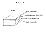
- Figure 1 shows a perspective view illustrating the construction of a carbonaceous thin film/n-type silicon multilayer sample of the present invention.
- Figure 2 shows an I-V characteristic diagram of a carbonaceous thin film/n-type silicon multilayer sample as an embodiment.
- Figure 3 shows a semi-logarithmic I-V characteristic diagram of a carbonaceous thin film/n-type silicon multilayer sample as an embodiment.
- Figure 4 shows a spectroscopic characteristic diagram of a carbonaceous thin film/n-type silicon multilayer sample as an embodiment.
- Figure 5 shows a relational diagram illustrating an absorption spectrum of a carbonaceous thin film as an embodiment.
- Figure 6 shows a schematic view illustrating the junction band structure of a 500°C carbonaceous thin film/n-type silicon multilayer sample as an embodiment.
- Figure 7 shows a temperature characteristic diagram illustrating for the optical band gap Eopt of a carbonaceous thin film as an embodiment.
- the present invention permits achievement of a novel semiconductor element not known so far by the use of the chemically vapor-deposited carbonaceous thin film and the n-type or p-type semiconductor substrate as described above, and allows application thereof to, for example, a diode, a rectifier element, a photodiode, an optical sensor and a solar cell.
- any n-type or p-type semiconductor substrate may be used: monocrystalline silicon, polycrystalline silicon, amorphous silicon, or compound semiconductor, or other n-type or p-type semiconductor substrate corresponding to any one thereof, in the form of a sheet or a thin film.
- the carbonaceous thin film to be chemically vapor-deposited (CVD) on such a semiconductor substrate may be formed from at least a kind of organic compound, particularly a carbocyclic organic compound as the raw material in the present invention.
- This carbocyclic organic compound may be selected from a wide range of kinds of compounds including hexacyclic benzene compounds and pentacyclic or septocyclic no-benzene compounds. Even a monocyclic or polycyclic organic compound including a pentacyclic or septocyclic one may be preferably employed in the present invention.
- any compound selected from a quinone hexacyclic compound such as 2,5-dimethyl-p-benzoquinone of the following formula:
- an organic compound containing such atoms as oxygen, nitrogen, boron, phosphorus and halogen as hetero-elements may be used as a kind of carbocyclic compound.
- a carbonaceous thin film of the present invention can be formed on said n-type or p-type semiconductor substrate by thermochemical vapor deposition.
- a material different from the carbon source material may be used as the source materials of the above-mentioned hetero-atom in the form of doping.
- the chemically vapor-deposited carbonaceous thin film should preferably comprise at least 80% (weight percentage) carbon. With a carbon content of under 80%, it is difficult to obtain a desired element having marked or stable properties as desired.
- the carbonaceous thin film should mainly comprise a non-diamond structure.
- the structure commonly known as the diamond structure, exhibiting insulating property, is naturally named as such.
- the non-diamond structure is considered to be formed by a structure in which a conjugate system of the carbonaceous compound in the above-mentioned carbonaceous thin film sufficiently expands.
- a preferable embodiment comprises, a carbocyclic organic compound as the raw material and a temperature up to 1000°C.
- the heterojunction type or Schottky-barrier type semiconductor element provided by the present invention has specific photoelectric characteristics and is expected to be applied to a solar cell or the like.
- n-type silicon monocrystalline wafer with phosphorus (P) as dopant having a thickness of 0.5 mm, was used as the substrate.
- the substrate Prior to depositing a carbonaceous thin film, the substrate was washed with fluoric acid in a concentration of 20%.
- the raw material for CVD reaction was 2,5-dimethyl-p-benzoquinone.
- the CVD reaction was caused under the following conditions under the atmospheric pressure: Substrate temperature: 500°C Material vaporizing temperature: 110°C Carrier gas: argon Depositing time: 90 minutes
- the thus deposited carbonaceous thin film had a thickness of about 400 ⁇ .
- alloy electrodes were attached to the back of the silicon substrate by ultrasonic welding.
- a gold thin film having a thickness of 80 to 100 ⁇ was vacuum-deposited on the surface of the carbonaceous thin film to form a surface electrode.
- the structure of the thus prepared cell sample is illustrated in Fig. 1.
- Fig. 2 shows current-voltage (I-V) characteristics of the prepared carbonaceous thin film/n-type silicon multilayer cell sample. Without light irradiation, this sample exhibits rectifying I-V characteristics.
- I-V current-voltage
- the sample When irradiating a light (Xe arc lamp) having a wavelength 400 to 850 nm and a power of 15 mW/cm2 onto it, the sample generated short-circuit current I sc of about 2.73 mA/cm2 and open-circuit voltage V oc of 325 mV.
- the fill factor value ff as derived from the I-V curve is about 0.65 and the energy conversion efficiency ⁇ is about 3.8%.
- Fig. 3 shows I-V characteristics of the sample without light irradiation, as measured at room temperature, in the form of a semi-logarithmic graph.
- the current-voltage relationship of the linear portion gives an ideality factor n and a dark current I o , as determined by the following formula, of 1.10 and 1.5 x 10 ⁇ 5 mA/cm2, respectively:
- Fig. 4 illustrates dependence on light wavelength (also known as spectroscopic characteristic) of short-circuit current and open-circuit voltage of this sample.
- This sample generates an almost constant photocurrent within a wavelength range of from 500 to 950 nm. This suggests the possibility of highly efficiently utilizing solar energy by the carbonaceous thin film/n-type silicon multilayer cell, and permits confirmation that this cell constitutes a solar cell or the like as an element known as a photoelectric transducer.
- the substrate Prior to depositing a carbonaceous thin film, the substrate was washed with fluoric acid in a concentration of 20%.
- the raw material for CVD reaction was ⁇ , ⁇ '-dichloro-p-xylene.
- the CVD reaction was caused under the atmospheric pressure under the following conditions: Substrate temperature: 800°C Material vaporizing temperature: 100°C Carrier gas: argon Depositing time: 120 minutes
- the resultant carbonaceous thin film had a thickness of about 500 ⁇ .
- alloy electrodes were attached to the back of the substrate by ultrasonic welding.
- gold was vacuum-deposited into a thickness of 80 to 100 ⁇ on the surface of the carbonaceous thin film as a sufrace electrode.
- this sample When light was not irradiated, this sample showed rectifying I-V characteristics.
- irradiating light Xe arc lamp
- the sample When irradiating light (Xe arc lamp) of a wavelength of 400 to 850 nm and a power of 40 mW/cm2, the sample generated short-circuit current I sc of about 0.26 mA/cm2 and open-circuit voltage V oc of 68 mV.
- the optical band gap E opt of the 500°C carbonaceous thin film as determined by this Formula (2) is about 0.25 eV.
- the 500°C carbonaceous thin film has a band gap of 0.25 eV, as described above.
- the junction type of the carbonaceous thin film/silicon multilayer sample is considered to be heterojunction.
- a typical junction band structure of the 500°C carbonaceous thin film/n-type silicon multilayer sample is shown in Fig. 6.
- Fig. 7 shows the optical band gap Eopt of carbonaceous thin film.
- the carbonaceous thin film heat-treated at a temperature of up to 580°C shows a positive optical band gap Eopt, the optical band gap Eopt changes into a negative one at a temparature of over 580°C.
- junction type of the carbonaceous thin film/semiconductor multilayer sample made at a temperature of up to 580°C is considered to be heterojunction type, and one made at a temperature of over 580°C is considered to be Schottky-barrier type.
- a heterojunction type or Schottky-barrier type semiconductor element comprising a chemical vapor-deposited (CVD) carbonaceous thin film and an n-type or p-type semiconductor substrate was successfully prepared.
- CVD chemical vapor-deposited
Abstract
The present invention provide a heterojunction type or Schottky-barrier type semiconductor element wherein a carbonaceous thin film is chemically vapor-deposited on an n-type or p-type semiconductor substrate and a solar cell or the like as an application thereof.
Description
- The present invention relates to a heterojunction type or Schottky-barrier type semiconductor element and a solar cell. More particularly, the present invention relates to a novel heterojunction type or Schottky-barrier type semiconductor element comprising a carbonaceous thin film, which is applicable as an electronic device, a solar cell and so on.
- Various semiconductor elements have so far been developed as electronic devices, optoelectric transducers and solar cells, and research efforts have actively been made to sophisticate functions thereof and to find new applications based on new properties derived from new combinations of materials.
- While, among these semiconductor elements, silicon semiconductors or compound semiconductors have formed the main current, research on organic semiconductors has recently made a marked progress.
- Carbonaceous materials typically represented by graphite, on the other hand, having excellent chemical, mechanical, biological and electronic properties are known to be applicable in a wide range of areas including space technology, sporting goods, and biological materials. Furthermore, the important role which may be played by carbonaceous π electronic materials as next-generation electronic materials is now entertained, in view of such electronic properties as ultra-high speed electron mobility and ultra-polarizability of graphite.
- From the point of view of physics, carbonaceous materials come under the category of semiconductor materials. In general, for example, the carbonaceous materials heat-treated at a temperature of up to 800°C shows a positive Hall constant. According as the heat-treatment temperature becomes higher, the Hall constant decreases and changes into a negative one at a temperature of over 800°C. The sign of Hall constant once changes into positive at about 1,600°C along with a further increase in temperature, and changes again into negative at 2,400°C. This property of the carbonaceous materials suggests the possibility of making an electronic device by utilizing this property.
- However, practical application of graphite to electronic materials, particularly to electronic devices has not as yet been achieved to date. The main reason is that a high graphite formation temperature of over 2,500°C is required in general. As compared with monocrystalline graphite, amorphous one can be formed at a far lower temperature. Particularly, a thin (<1,000 Å) amorphous carbon thin film produced by the CVD method can have a high electric conductivity (usually within a range of from about 10⁻⁴ to 10³ S/cm) through a heat treatment at a temperature of under 1,000°C, and exhibits a light transmissivity to some extent. This suggests the possibility of application as an electronic device material, particularly, as a solar cell material.
- The solar cells practically used at present mainly comprise silicon semiconductor and compound semiconductor, but not one made of organic materials. On the other hand, however, active research efforts have been made on solar cells utilizing organic thin films since invention of conductive polyacetylene in 1977. A major problem involved in current organic solar cells is that they are poor in stability and low in energy cenversion ratio.
- Various findings to be noted have been reported on carbonaceous materials with increasing expectation as semiconductor materials. But studies or reports teaching achievement of more concrete and practicable semiconductor elements have not as yet been made.
- In view of the circumstances as described above, therefore, the present invention has an object to provide means to permit achievement of a semiconductor element by a new approach to carbonaceous materials. More specifically, the present invention has an object to achieve an optoelectric conversion diode and a solar cell using an amorphous carbonaceous thin film as an application of carbonaceous materials to electronic devices.
- As means to solve the problems as described above, the present invention provides a heterojunction type or Schottky-barier type semiconductor element wherein a carbonaceous thin film is chemically vapor-deposited (CVD) on an n-type or p-type semiconductor substrate and a solar cell as an application thereof.
- Figure 1 shows a perspective view illustrating the construction of a carbonaceous thin film/n-type silicon multilayer sample of the present invention.
- Figure 2 shows an I-V characteristic diagram of a carbonaceous thin film/n-type silicon multilayer sample as an embodiment.
- Figure 3 shows a semi-logarithmic I-V characteristic diagram of a carbonaceous thin film/n-type silicon multilayer sample as an embodiment.
- Figure 4 shows a spectroscopic characteristic diagram of a carbonaceous thin film/n-type silicon multilayer sample as an embodiment.
- Figure 5 shows a relational diagram illustrating an absorption spectrum of a carbonaceous thin film as an embodiment.
- Figure 6 shows a schematic view illustrating the junction band structure of a 500°C carbonaceous thin film/n-type silicon multilayer sample as an embodiment.
- Figure 7 shows a temperature characteristic diagram illustrating for the optical band gap Eopt of a carbonaceous thin film as an embodiment.
- The present invention permits achievement of a novel semiconductor element not known so far by the use of the chemically vapor-deposited carbonaceous thin film and the n-type or p-type semiconductor substrate as described above, and allows application thereof to, for example, a diode, a rectifier element, a photodiode, an optical sensor and a solar cell.
- There is no particular limitation on the kind of the semiconductor substrate which constitutes the heterojunction type semiconductor element, but any n-type or p-type semiconductor substrate may be used: monocrystalline silicon, polycrystalline silicon, amorphous silicon, or compound semiconductor, or other n-type or p-type semiconductor substrate corresponding to any one thereof, in the form of a sheet or a thin film.
- The carbonaceous thin film to be chemically vapor-deposited (CVD) on such a semiconductor substrate may be formed from at least a kind of organic compound, particularly a carbocyclic organic compound as the raw material in the present invention. This carbocyclic organic compound may be selected from a wide range of kinds of compounds including hexacyclic benzene compounds and pentacyclic or septocyclic no-benzene compounds. Even a monocyclic or polycyclic organic compound including a pentacyclic or septocyclic one may be preferably employed in the present invention.
- For example, as such carbocyclic organic compound, any compound selected from a quinone hexacyclic compound such as 2,5-dimethyl-p-benzoquinone of the following formula:
-

or decacyclene having a more complicated ring system of the following formula: -

may be used. - In the present invention, apart from one or more carbocyclic compounds used as raw materials, a chain carbon compound, or as required, an organic compound containing such atoms as oxygen, nitrogen, boron, phosphorus and halogen as hetero-elements may be used as a kind of carbocyclic compound. These constituents make the carbonaceous thin film more interesting.
- While chemical vapor deposition (CVD) can be applied by using any of these materials serving as the carbon source, the reaction may be caused thermally, or separately from, or in combination with excitation by a light or plasma. Most simply, a carbonaceous thin film of the present invention can be formed on said n-type or p-type semiconductor substrate by thermochemical vapor deposition. In this film formation, a material different from the carbon source material may be used as the source materials of the above-mentioned hetero-atom in the form of doping.
- For the purpose of constructing the heterojunction type or Schottky-barrier type semiconductor element of the present invention, the chemically vapor-deposited carbonaceous thin film should preferably comprise at least 80% (weight percentage) carbon. With a carbon content of under 80%, it is difficult to obtain a desired element having marked or stable properties as desired. The carbonaceous thin film should mainly comprise a non-diamond structure. The structure commonly known as the diamond structure, exhibiting insulating property, is naturally named as such. In the present invention, the non-diamond structure is considered to be formed by a structure in which a conjugate system of the carbonaceous compound in the above-mentioned carbonaceous thin film sufficiently expands.
- For example, in chemical vapor deposition from 2,5-dimethyl-p-benzoquinone and decacyclene described above, a carbonaceous thin film expressed in the following structural models are estimated to be formed:
-

-

When chemical vapor deposition is thermally conducted, a preferable embodiment comprises, a carbocyclic organic compound as the raw material and a temperature up to 1000°C. - The heterojunction type or Schottky-barrier type semiconductor element provided by the present invention has specific photoelectric characteristics and is expected to be applied to a solar cell or the like.
- It is needless to mention that various embodiments are possible as to the material for electrodes as semiconductor elements and their arrangement.
- Now therefore, the construction and effects of the present invention will be described further in detail by means of some examples.
- An n-type silicon monocrystalline wafer with phosphorus (P) as dopant, having a thickness of 0.5 mm, was used as the substrate. Prior to depositing a carbonaceous thin film, the substrate was washed with fluoric acid in a concentration of 20%. The raw material for CVD reaction was 2,5-dimethyl-p-benzoquinone. The CVD reaction was caused under the following conditions under the atmospheric pressure:
Substrate temperature: 500°C Material vaporizing temperature: 110°C Carrier gas: argon Depositing time: 90 minutes - The thus deposited carbonaceous thin film had a thickness of about 400 Å. In the resultant multilayer sample of carbonaceous thin film/n-type monocrystalline silicon, alloy electrodes were attached to the back of the silicon substrate by ultrasonic welding. In addition, a gold thin film having a thickness of 80 to 100 Å was vacuum-deposited on the surface of the carbonaceous thin film to form a surface electrode. The structure of the thus prepared cell sample is illustrated in Fig. 1.
- Fig. 2 shows current-voltage (I-V) characteristics of the prepared carbonaceous thin film/n-type silicon multilayer cell sample. Without light irradiation, this sample exhibits rectifying I-V characteristics. When irradiating a light (Xe arc lamp) having a
wavelength 400 to 850 nm and a power of 15 mW/cm² onto it, the sample generated short-circuit current Isc of about 2.73 mA/cm² and open-circuit voltage Voc of 325 mV. The fill factor value ff as derived from the I-V curve is about 0.65 and the energy conversion efficiency η is about 3.8%. - Fig. 3 shows I-V characteristics of the sample without light irradiation, as measured at room temperature, in the form of a semi-logarithmic graph. The current-voltage relationship of the linear portion gives an ideality factor n and a dark current Io, as determined by the following formula, of 1.10 and 1.5 x 10⁻⁵ mA/cm², respectively:
-

- A p-type silicon monocrystalline wafer, with boron (B) as dopant, having a thickness of 0.5 mm, was used as the substrate. Prior to depositing a carbonaceous thin film, the substrate was washed with fluoric acid in a concentration of 20%. The raw material for CVD reaction was α, α'-dichloro-p-xylene. The CVD reaction was caused under the atmospheric pressure under the following conditions:
Substrate temperature: 800°C Material vaporizing temperature: 100°C Carrier gas: argon Depositing time: 120 minutes - The resultant carbonaceous thin film had a thickness of about 500 Å. In the resultant multilayer sample of carbonaceous thin film/p-type monocrystalline silicon, alloy electrodes were attached to the back of the substrate by ultrasonic welding. In addition, gold was vacuum-deposited into a thickness of 80 to 100 Å on the surface of the carbonaceous thin film as a sufrace electrode.
- When light was not irradiated, this sample showed rectifying I-V characteristics. When irradiating light (Xe arc lamp) of a wavelength of 400 to 850 nm and a power of 40 mW/cm², the sample generated short-circuit current Isc of about 0.26 mA/cm² and open-circuit voltage Voc of 68 mV.
- An X-ray diffraction and a Raman analysis as applied to the 2,5-dimethyl-p-benzoquinone carbonaceous thin film deposited at 500°C in Example 1 demonstrated that the film had an amorphous-carbon structure. It has an electric conductivity of about 4.5 x 10⁻³ S/cm at the room temperature in the face direction. The contents of C, H and O as determined by element analysis were 87.2%, 0.37% and 12.4%, respectively. In Fig. 5 showing an absorption spectrum of the carbonaceous thin film, the one deposited at 500°C shows no intrinsic absorption peak, thus suggesting that this is an amorphous structure. The optical band gap Eopt and the absorption coefficient α of an amorphous semiconductor have the following relationship:
-

- The 500°C carbonaceous thin film has a band gap of 0.25 eV, as described above. The junction type of the carbonaceous thin film/silicon multilayer sample is considered to be heterojunction. A typical junction band structure of the 500°C carbonaceous thin film/n-type silicon multilayer sample is shown in Fig. 6.
- Fig. 7 shows the optical band gap Eopt of carbonaceous thin film. The carbonaceous thin film heat-treated at a temperature of up to 580°C shows a positive optical band gap Eopt, the optical band gap Eopt changes into a negative one at a temparature of over 580°C.
- For this reason, the junction type of the carbonaceous thin film/semiconductor multilayer sample made at a temperature of up to 580°C is considered to be heterojunction type, and one made at a temperature of over 580°C is considered to be Schottky-barrier type.
- According to the present invention, as described above in detail, a heterojunction type or Schottky-barrier type semiconductor element comprising a chemical vapor-deposited (CVD) carbonaceous thin film and an n-type or p-type semiconductor substrate was successfully prepared. As a result, the possibility was found to achieve quite a novel solar cell.
- It should be noted that the objects and advantages of the invention may be attained by means of any compatible combination(s) particularly pointed out in the items of the following summary of the invention and the appended claims.
-
- 1. A heterojunction type semiconductor element wherein a carbonaceous thin film is chemically vapor-deposited on an n-type or p-type semiconductor substrate.
- 2. A Schottky-barrier type semiconductor element wherein a carbonaceous thin film is chemicaly vapor-deposited on an n-type or p-type semiconductor substrate.
- 3. A heterojunction type or Schottky-barrier type semiconductor element wherein said semiconductor substrate is a sheet-type or thinfilm-type monocrystalline silicon, polycrystalline silicon, amorphous silicon, a compound semiconductor or an n-type or p-type semiconductor corresponding thereto.
- 4. A heterojunction type or Schottky-barrier type semiconductor element wherein said carbonaceous thin film comprises a thin film chemically vapor-deposited from at least a kind of carbonaceous organic compound.
- 5. A heterojunction type or Schottky-barrier type semiconductor element wherein said carbonaceous thin film has a carbon content of at least 80%.
- 6. A heterojunction type or Schottky-barrier type semiconductor element wherein said carbonaceous thin film substantially has a non-diamond structure.
- 7. A heterojunction type or Schottky-barrier type semiconductor element wherein said carbonaceous thin film contains heteroatoms such as oxygen, nitrogen, boron phosphorus and halogen.
- 8. A heterojunction type or Schottky-barrier type semiconductor element wherein said carbonaceous thin film is chemically vapor-deposited.
- 9. A heterojunction type or Schottky-barrier type semiconductor element wherein said carbonaceous thin film is chemically vapor-deposited at a range of from room temperature to 1000°C.
- 10. A solar cell which comprises the heterojunction type or Schottky-barrier type semiconductor element.
Claims (10)
- A heterojunction type semiconductor element wherein a carbonaceous thin film is chemically vapor-deposited on an n-type or p-type semiconductor substrate.
- A Schottky-barrier type semiconductor element wherein a carbonaceous thin film is chemicaly vapor-deposited on an n-type or p-type semiconductor substrate.
- A heterojunction type or Schottky-barrier type semiconductor element as claimed in claim or 1 or 2, wherein said semiconductor substrate is a sheet-type or thinfilm-type monocrystalline silicon, polycrystalline silicon, amorphous silicon, a compound semiconductor or an n-type or p-type semiconductor corresponding thereto.
- A heterojunction type or Schottky-barrier type semiconductor element as claimed in any one of claims 1 to 3, wherein said carbonaceous thin film comprises a thin film chemically vapor-deposited from at least a kind of carbonaceous organic compound.
- A heterojunction type or Schottky-barrier type semiconductor element as claimed in any one of claims 1 to 4, wherein said carbonaceous thin film has a carbon content of at least 80%.
- A heterojunction type or Schottky-barrier type semiconductor element as claimed in any one of claims 1 to 5, wherein said carbonaceous thin film substantially has a non-diamond structure.
- A heterojunction type or Schottky-barrier type semiconductor element as claimed in any one of claims 1 to 6, wherein said carbonaceous thin film contains heteroatoms such as oxygen, nitrogen, boron phosphorus and halogen.
- A heterojunction type or Schottky-barrier type semiconductor element as claimed in any one of claims 1 to 7, wherein said carbonaceous thin film is chemically vapor-deposited and preferably at a range of from room temperature to 1000°C.
- A solar cell which comprises the heterojunction type or Schottky-barrier type semiconductor element as claimed in any one of claims 1 to 9.
- A semiconductor element wherein a carbonaceous thin film is deposited on a semiconductor substrate.
Applications Claiming Priority (4)
| Application Number | Priority Date | Filing Date | Title |
|---|---|---|---|
| JP274781/94 | 1994-11-09 | ||
| JP27478194 | 1994-11-09 | ||
| JP280596/95 | 1995-10-27 | ||
| JP28059695 | 1995-10-27 |
Publications (1)
| Publication Number | Publication Date |
|---|---|
| EP0714136A1 true EP0714136A1 (en) | 1996-05-29 |
Family
ID=26551195
Family Applications (1)
| Application Number | Title | Priority Date | Filing Date |
|---|---|---|---|
| EP95117698A Withdrawn EP0714136A1 (en) | 1994-11-09 | 1995-11-09 | Heterojunction type or Schottky-barrier type semiconductor element and solar cell |
Country Status (1)
| Country | Link |
|---|---|
| EP (1) | EP0714136A1 (en) |
Cited By (6)
| Publication number | Priority date | Publication date | Assignee | Title |
|---|---|---|---|---|
| KR100421650B1 (en) * | 1998-06-15 | 2004-03-10 | 키시모토 상교 컴퍼니 리미티드 | Insulating film for semiconductor device and semiconductor device |
| WO2005081296A1 (en) * | 2004-02-10 | 2005-09-01 | Infineon Technologies Ag | Method for depositing a conductive carbon material on a semiconductor for forming a schottky contact and semiconductor contact device |
| US7768016B2 (en) | 2008-02-11 | 2010-08-03 | Qimonda Ag | Carbon diode array for resistivity changing memories |
| US7894253B2 (en) | 2006-10-27 | 2011-02-22 | Qimonda Ag | Carbon filament memory and fabrication method |
| US7915603B2 (en) | 2006-10-27 | 2011-03-29 | Qimonda Ag | Modifiable gate stack memory element |
| US8030637B2 (en) | 2006-08-25 | 2011-10-04 | Qimonda Ag | Memory element using reversible switching between SP2 and SP3 hybridized carbon |
Citations (1)
| Publication number | Priority date | Publication date | Assignee | Title |
|---|---|---|---|---|
| EP0472054A1 (en) * | 1990-08-20 | 1992-02-26 | Siemens Aktiengesellschaft | Photocell containing hydrogenated amorphous carbon |
-
1995
- 1995-11-09 EP EP95117698A patent/EP0714136A1/en not_active Withdrawn
Patent Citations (1)
| Publication number | Priority date | Publication date | Assignee | Title |
|---|---|---|---|---|
| EP0472054A1 (en) * | 1990-08-20 | 1992-02-26 | Siemens Aktiengesellschaft | Photocell containing hydrogenated amorphous carbon |
Non-Patent Citations (5)
| Title |
|---|
| BHAGAVAT G K ET AL: "Semiconducting amorphous carbon films and carbon-single-crystal silicon heterojunctions", THIN SOLID FILMS, vol. 64, no. 1, N SOLID FILMS, 15 NOV. 1979, SWITZERLAND, pages 57 - 62, XP024655774, DOI: doi:10.1016/0040-6090(79)90543-1 * |
| CHAN K K ET AL: "ELECTRONIC PROPERTIES OF SEMICONDUCTING DIAMOND-LIKE CARBON-DIAMOND", THIN SOLID FILMS, vol. 212, no. 1 / 2, 15 May 1992 (1992-05-15), pages 232 - 239, XP000360220 * |
| GILDENBLAT G S ET AL: "ELECTRICAL CHARACTERISTICS OF SCHOTTKY DIODES FABRICATED USING PLASMA ASSISTED CHEMICAL VAPOR DEPOSITED DIAMOND FILMS", APPLIED PHYSICS LETTERS, vol. 53, no. 7, 15 August 1988 (1988-08-15), pages 586 - 588, XP000118691 * |
| HWANG S B ET AL: "AMORPHOUS CARBON/CRYSTALLINE SILICON HIGH VOLTAGE HETEROJUNCTION DIODE PREPARED BY PHOTOCHEMICAL VAPOUR DEPOSITION", ELECTRONICS LETTERS, vol. 27, no. 22, 24 October 1991 (1991-10-24), pages 2043 - 2045, XP000253714 * |
| KONOFAOS N ET AL: "AMORPHOUS DIAMONDLIKE CARBON-SILICON HETEROJUNCTION DEVICES FORMED BY ION IMPLANTATION", APPLIED PHYSICS LETTERS, vol. 61, no. 23, 7 December 1992 (1992-12-07), pages 2805 - 2807, XP000335074 * |
Cited By (6)
| Publication number | Priority date | Publication date | Assignee | Title |
|---|---|---|---|---|
| KR100421650B1 (en) * | 1998-06-15 | 2004-03-10 | 키시모토 상교 컴퍼니 리미티드 | Insulating film for semiconductor device and semiconductor device |
| WO2005081296A1 (en) * | 2004-02-10 | 2005-09-01 | Infineon Technologies Ag | Method for depositing a conductive carbon material on a semiconductor for forming a schottky contact and semiconductor contact device |
| US8030637B2 (en) | 2006-08-25 | 2011-10-04 | Qimonda Ag | Memory element using reversible switching between SP2 and SP3 hybridized carbon |
| US7894253B2 (en) | 2006-10-27 | 2011-02-22 | Qimonda Ag | Carbon filament memory and fabrication method |
| US7915603B2 (en) | 2006-10-27 | 2011-03-29 | Qimonda Ag | Modifiable gate stack memory element |
| US7768016B2 (en) | 2008-02-11 | 2010-08-03 | Qimonda Ag | Carbon diode array for resistivity changing memories |
Similar Documents
| Publication | Publication Date | Title |
|---|---|---|
| Matsuyama et al. | Preparation of high-quality n-type poly-Si films by the solid phase crystallization (SPC) method | |
| US4459163A (en) | Amorphous semiconductor method | |
| Krishna et al. | Photovoltaic and spectral photoresponse characteristics of n-C/p-C solar cell on ap-silicon substrate | |
| Yu et al. | Photovoltaic cell of carbonaceous film/n‐type silicon | |
| Saitoh et al. | Optical and electrical properties of amorphous silicon films prepared by photochemical vapor deposition | |
| EP0233613B1 (en) | Deposition feedstock and dopant materials useful in the fabrication of hydrogenated amorphous silicon alloys for photovoltaic devices and other semiconductor devices | |
| Krishna et al. | Photovoltaic solar cell from camphoric carbon A natural source | |
| US4690830A (en) | Activation by dehydrogenation or dehalogenation of deposition feedstock and dopant materials useful in the fabrication of hydrogenated amorphous silicon alloys for photovoltaic devices and other semiconductor devices | |
| Krishna et al. | Solar cells based on carbon thin films | |
| JPH07123111B2 (en) | Method for manufacturing semiconductor film and method for manufacturing photovoltaic structure | |
| Tian et al. | A photovoltaic cell from p-type boron-doped amorphous carbon film | |
| Mathew et al. | Structural and opto-electronic properties of electrodeposited CdTe on stainless steel foil | |
| Miller et al. | Preparation of stable efficient CdSe films for solar PEC cells | |
| EP0714136A1 (en) | Heterojunction type or Schottky-barrier type semiconductor element and solar cell | |
| HU187713B (en) | Method for producing semiconducting amorphous thin layers particularly for semiconductor devices | |
| Koltun et al. | Solar cells from Carbon | |
| Tian et al. | The aC: H/p-Si solar cell deposited by pulsed laser deposition | |
| Rusop et al. | Photovoltaic properties of nC: P/p-Si cells deposited by XeCl eximer laser using graphite target | |
| JP2980546B2 (en) | Semiconductor devices and solar cells | |
| Goswami | Three Generations of Solar Cells | |
| Weisz et al. | The compositional dependence of the optical and electrical properties of hydrogenated amorphous Si-Ge films prepared by co-sputtering | |
| von Huth et al. | Diamond/CdTe: a new inverted heterojunction CdTe thin film solar cell | |
| Honda et al. | Amorphous Carbon-Based Semiconductor Capable of Controlling Its Optical Gap and Conductivity by Incorporating Silicon and Nitrogen Atoms | |
| Faiman et al. | Solar cells from C60 | |
| Yoshinaga et al. | Fabrication of silicon and carbon based wide-gap semiconductor thin films for high conversion efficiency |
Legal Events
| Date | Code | Title | Description |
|---|---|---|---|
| PUAI | Public reference made under article 153(3) epc to a published international application that has entered the european phase |
Free format text: ORIGINAL CODE: 0009012 |
|
| AK | Designated contracting states |
Kind code of ref document: A1 Designated state(s): DE FR IT |
|
| 17P | Request for examination filed |
Effective date: 19961126 |
|
| 17Q | First examination report despatched |
Effective date: 19981028 |
|
| STAA | Information on the status of an ep patent application or granted ep patent |
Free format text: STATUS: THE APPLICATION HAS BEEN WITHDRAWN |
|
| 18W | Application withdrawn |
Withdrawal date: 20000614 |