EP0714231A2 - Component tray and handling apparatus - Google Patents
Component tray and handling apparatus Download PDFInfo
- Publication number
- EP0714231A2 EP0714231A2 EP95307485A EP95307485A EP0714231A2 EP 0714231 A2 EP0714231 A2 EP 0714231A2 EP 95307485 A EP95307485 A EP 95307485A EP 95307485 A EP95307485 A EP 95307485A EP 0714231 A2 EP0714231 A2 EP 0714231A2
- Authority
- EP
- European Patent Office
- Prior art keywords
- tray
- base portion
- integrated circuit
- component
- Prior art date
- Legal status (The legal status is an assumption and is not a legal conclusion. Google has not performed a legal analysis and makes no representation as to the accuracy of the status listed.)
- Ceased
Links
- 238000003780 insertion Methods 0.000 claims description 4
- 230000037431 insertion Effects 0.000 claims description 4
- 230000032258 transport Effects 0.000 abstract description 2
- 239000000463 material Substances 0.000 description 4
- 239000011159 matrix material Substances 0.000 description 3
- 238000004806 packaging method and process Methods 0.000 description 3
- 230000004913 activation Effects 0.000 description 1
- 230000002411 adverse Effects 0.000 description 1
- 230000000994 depressogenic effect Effects 0.000 description 1
- 238000009434 installation Methods 0.000 description 1
- 238000000034 method Methods 0.000 description 1
- 230000001681 protective effect Effects 0.000 description 1
- 239000004065 semiconductor Substances 0.000 description 1
Images

Classifications
-
- H—ELECTRICITY
- H05—ELECTRIC TECHNIQUES NOT OTHERWISE PROVIDED FOR
- H05K—PRINTED CIRCUITS; CASINGS OR CONSTRUCTIONAL DETAILS OF ELECTRIC APPARATUS; MANUFACTURE OF ASSEMBLAGES OF ELECTRICAL COMPONENTS
- H05K13/00—Apparatus or processes specially adapted for manufacturing or adjusting assemblages of electric components
- H05K13/0084—Containers and magazines for components, e.g. tube-like magazines
-
- H—ELECTRICITY
- H01—ELECTRIC ELEMENTS
- H01L—SEMICONDUCTOR DEVICES NOT COVERED BY CLASS H10
- H01L23/00—Details of semiconductor or other solid state devices
-
- H—ELECTRICITY
- H01—ELECTRIC ELEMENTS
- H01L—SEMICONDUCTOR DEVICES NOT COVERED BY CLASS H10
- H01L2221/00—Processes or apparatus adapted for the manufacture or treatment of semiconductor or solid state devices or of parts thereof covered by H01L21/00
- H01L2221/67—Apparatus for handling semiconductor or electric solid state devices during manufacture or treatment thereof; Apparatus for handling wafers during manufacture or treatment of semiconductor or electric solid state devices or components; Apparatus not specifically provided for elsewhere
- H01L2221/683—Apparatus for handling semiconductor or electric solid state devices during manufacture or treatment thereof; Apparatus for handling wafers during manufacture or treatment of semiconductor or electric solid state devices or components; Apparatus not specifically provided for elsewhere for supporting or gripping
- H01L2221/68304—Apparatus for handling semiconductor or electric solid state devices during manufacture or treatment thereof; Apparatus for handling wafers during manufacture or treatment of semiconductor or electric solid state devices or components; Apparatus not specifically provided for elsewhere for supporting or gripping using temporarily an auxiliary support
- H01L2221/68313—Auxiliary support including a cavity for storing a finished device, e.g. IC package, or a partly finished device, e.g. die, during manufacturing or mounting
Definitions
- the present invention relates generally to handling, packaging, storing and shipping integrated circuit components or chips and, more particularly, to a tray for housing one or more chips and protecting the chip against damage and to an apparatus for accurately placing a chip within the tray without causing damage to the chip.
- Integrated circuit components or chips typically are made of semiconductor material and include a desired electrical circuit formed therein.
- the chips also typically include numerous electrical leads extending therefrom and are very fragile and sensitive to adverse handling.
- Such chips are transported from the chip manufacturer in bulk to electronics manufacturers, chip distributors or the like. Distributors typically break a bulk of chips into smaller quantities for shipment to small manufacturers, resellers, repair facilities, individual users etc.
- a distributor In order to protect smaller quantities of chips against damage, a distributor typically places one or more chips in some type of tray or other container and packages the tray and chip for shipping. If more than one tray is required, existing trays typically are arranged in a stack and are banded together with tape or some type of strap, as illustrated in Figure 2, to prevent the stack from falling apart and causing damage to the chips.
- Trays for use with such automated pick-and-place systems rely on positioning of existing trays from a chamfered corner of the tray. Such corner positioning, however, is not precise due to the tolerances involved and can lead to mis-positioning and damage to the chips.
- the invention also provides a cost effective apparatus for use by a distributor or the like to transfer chips from bulk containers to the trays without damaging the chips or associated electrical leads.
- the invention provides for safe handling, packaging, storing and shipping of integrated circuit components or chips, particularly for smaller quantities of chips, which typically is useful for chip distributors.
- a tray is provided for housing one or more chips in a protective manner.
- an apparatus is provided for accurately and safely transferring chips from bulk storage containers or the like to the tray.
- the tray of the invention is designed to be stackable with one or more other like trays and includes a locking member to secure the trays together.
- the locking member is readily activated by a user, preferably in a "twist-lock" manner and does not damage the chips in the tray.
- two trays are secured where a bottom tray holds a desired number of chips and the top tray is empty and merely serves as a cover to retain and protect chips in the bottom tray.
- the transfer apparatus of the invention preferably is a manually activated pick-and-place type mechanism that readily can be activated by a user to transport chips from a bulk tray or similar container to the tray of the invention. Upon holding of a chip by a vacuum head, an operator can readily position the chip for exact placement with respect to the tray which is precisely positioned on the apparatus for accurate placement.
- the device and apparatus of this invention are described in typical operating positions and terms such as upper, lower, horizontal etc. are utilized with reference to these positions. It will be understood, however, that the device and apparatus of this invention may be manufactured, stored, transported and sold in an orientation other than the positions described.
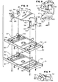
- a tray of the invention is generally designated by the reference numeral 10.
- the tray 10 is utilized to house one or more integrated circuit chips 12 to protect the chip 12 during handling, packaging, storing and shipping.
- the tray 10 can be stacked- to provide a top cover to the bottom tray 10 or to increase the number of chips 12 in a particular shipment.
- a twist-lock fastening or engagement member 14, illustrated in Figure 5 is utilized.
- the tray 10 preferably is designed for use with a pick-and-place mechanism 16 that accurately assembles chips 12 to the tray 10 without damaging the chip 12.
- the mechanism 16 preferably is manually activated, is substantially portable and moves chips 12 from bulk containers 18 to the tray 10 as described in detail below.
- the tray 10 is substantially rectangular in shape and is integrally formed from plastic or similar material.
- the material of the tray 10 is heat resistant to enable processing of the chip 12 within the tray 10 if desired.
- the tray 10 includes a predetermined number of pockets or sockets 20, one each for a respective chip 12. Although four pockets 20 are illustrated, the number of pockets 20 can vary as desired.
- Each pocket 20 is configured to accept the particular shape of the chip 12 which in this embodiment is square.
- the particular shape of the pocket 20, however, can vary to accommodate the chip 12.
- the pockets 20 are inter-connected by a base portion 22 and an outer frame portion 24.
- the base portion 22 is configured to accept the twist-lock engagement member 14 while the outer frame portion 24 adds stability to the tray 10 as well as spacing and stacking of trays 10.
- Each pocket 20 includes a base 26, an upstanding square or rectangular platform 28 and a central aperture 30 through the platform 28.
- the platform 28 supports a body 12a of the chip 12 while "gull-wing" type leads 12b of the chip 12 can extend over the edge of the platform 28.
- each tray 10 includes one or more alignment or registration notches 32 positioned on the exterior surface of the outer frame portion 24.
- the notch 32 provides a seat for a corresponding pin of the mechanism 16 to precisely position the tray 10 with respect to the mechanism 16 as explained in detail below.
- the tray 10 includes three notches 32.
- One notch 32a is positioned on a first minor side 34 of the tray 10 and two notches 32b and 32c are positioned on a second opposite minor side 36 of the tray 10.
- Two opposing major sides 38 and 40 of the tray 10 preferably do not include any notches 32.
- the notches 32b and 32c are positioned equidistant from a longitudinal axis of the tray 10 and the notch 32a is aligned with the notch 32b.
- the notches 32 provide alignment with respect to the centre-line of the tray 10, rather than the corners or edges thereof, which provides increased accuracy in positioning the tray 10 on the mechanism 16.
- a top side 42 of each tray 10 includes an upstanding ridge 44 about its periphery having at least one cut-out 46.
- a bottom side 48 of each tray 10 includes a depending ridge 50 about its periphery having at least one protrusion S2 for seating within the cut-out 46.
- a cut-out 46 and corresponding protrusion 52 are provided along each side 34-40 proximate the middle thereof. It is to be understood, however, that the number, size, shape and position of the cut-out 46 and protrusion 52 can vary so long as they cooperate to provide the desired stacking.
- the twist-lock engagement member 14 can be utilized.
- the engagement member 14 includes a base member 54 and preferably four integrally formed leg members 56 depending from a side thereof.
- the leg members 56 extend through apertures 58 formed in the base 22 of the trays 10 and are secured to a back side 60 of a tray 10 as described herein.
- Each leg member 56 includes a first proximal end 62 connected to the base 54 and a second opposite distal end 64.
- the length of the leg members 56 is selected for accommodating two trays 10, but the number of trays 10 accommodated by the leg members 56 can vary.
- the distal end 64 of the leg members 56 includes a ball member 66 connected to the leg members 56 by a member 68 extending transverse to each leg member 56.
- the ball members 66 seat within corresponding sockets 70 formed in the back side 60 of the tray 10.
- the engagement member 14 is twisted clockwise until each ball member 66 is seated within a respective socket 70.
- the base member can include a slot 72 for a screwdriver or similar article.
- the engagement member 14 merely is twisted counter clockwise to disengage the ball members 66 from the sockets 70.
- the leg members 56 then are removed from the apertures 58.
- the engagement member 14 provides clamping of the centre of the trays 10 which are designed for slight flexing of the base 22 of the trays 10 during installation of the engagement member 14.
- the flexing enables the engagement member 14 to move into position and prevents a top tray 10 from damaging a chip 12 in a bottom tray 10 of the stack.
- flexing of the base portion 22 provides increased gripping of the outer frame portion 24 to increase the stability of the stack.
- a top tray 10 in the stack does not contain any chips 12 and merely serves as a cover to maintain and protect the chips 12 in a bottom tray 10 of a stack. If desired, however, chips 12 can be placed in a top tray 10 of a stack and secured thereto in another manner.
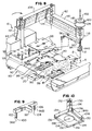
- the mechanism 16 is preferably designed for orthogonal movement and substantially includes a base 80, a movable arm 82 and an integrated circuit chip alignment and gripping head assembly 84 having a head portion 84a.
- the head assembly 84 includes a slight suction which holds a chip 12 for removal from a bulk storage container or tray 18 and placement within a pocket 20 of a tray 10.
- the mechanism 16 substantially is manually activated and precisely positions the chips 12 without damage to the chips 12 or the leads 12b.
- the base 80 includes a first portion 86 for placement of one or more trays 10 and a second portion 88 for placement of chips 12 carried by the bulk carrier container or tray 18.
- the first portion 86 includes two engagement pins 90 for each tray 10 positioned for insertion with the notches 32a and 32b of the tray 10.
- the pins 90 precisely position the trays 10 on the base 80 so that the trays 10 cannot readily move thereon. It is to be noted that the pins 90 and/or notches 32 can be replaced with any other elements so long as the desired precise positioning with respect to a centre-line of the tray 10 is provided.
- the mechanism 16 includes a positioning system including a locator arm 92 in operable connection with the head assembly 84 and a corresponding location plate 94 on the base 80.
- the locator arm 92 includes two locator pins 96 for insertion within desired corresponding apertures 98 positioned within the location plate 94.
- the head 84a of the head assembly 84 is precisely positioned for placement of a chip 12 within a desired pocket 20 of a tray 10.
- one pin 96a has a ball tip 100 with a relieved shaft 102 above the ball 100 while the other pin 96b is formed as a flattened spear tip 104 with a full size shaft 106 above the spear tip 104.
- the movable arm member 82 includes first and second portions 108 and 110 having a belt system therein for providing the orthogonal movement as is known in the art.
- the first portion 108 is connected to the base 80 through a support 112 and a vacuum line 114 runs through the first and second portions 108 and 110 for attachment to the head assembly 84.
- a pick-up assembly 116 is connected to a distal end 118 of the second portion 110 to which the head assembly 84 and the locator arm 92 are secured. Additionally, to assist an operator in positioning the arm 82, a finger wheel 120 is positioned atop the pick up assembly 116.
- the finger wheel 120 preferably includes a button 122 for activation of the vacuum line 114 with respect to the head 84a.
- the button 122 preferably includes a groove 124 formed therein.
- the pick-up assembly 116 includes a first spring (not illustrated) mounted therein for assisting in raising and lowering the entire arm 82 for pick up of the chip 12 and movement thereof. Additionally, to assist an operator in "feeling" the location of the chip 12 and preventing damage to the leads 12b of the chip 12, a light spring (not illustrated) is positioned within the head assembly 84.
- the head 84a includes a stem 126 and a chip engagement portion 128.
- the stem 126 includes a groove 130 positioned about its periphery for snapping engagement of the stem 126 to the pick-up assembly 116.
- the groove 130 includes a detent 132 for seating of a corresponding member (not illustrated) within the pick-up assembly 116.
- the chip engagement portion 128 conforms to the shape of the chip 12 and, in this embodiment, is a substantially square or rectangular planar member including depending side walls 134 positioned about its periphery. To assist in locating the head 84a with respect to a chip 12, the walls 134 are tapered outward. Additionally, to enable release of the chip 12 upon vacuum cut off from an aperture 138 and ensure that the vacuum will not hold unless the chip 12 is properly positioned, the side walls 134 include a passage 136 proximate each corner.
- one or more empty trays 10 are positioned on the first portion 86 of the base 80 and a bulk matrix tray 18 with a potentially large number of chips 12 is positioned on the second portion 88 of the base 80.
- An operator grips the finger wheel 120 and moves the arm 82 to position the head 84 above a chip 12 positioned in the bulk matrix tray 18.
- the head 84 is lowered and the chip 12 is positioned within the confines of the side walls 134 for engagement with the vacuum from the aperture 138.
- the vacuum takes hold and the chip 12 can be lifted out of the bulk matrix tray 18 upon lifting of the finger wheel 120 and arm 82 such as in the direction of arrow "A", for example.
- the arm 82, head assembly 84 and head 84a are then moved in the direction of arrow "B", for example, to a position above a pocket 20 of a tray 10.
- the pins 96 of the locator arm 92 align with apertures 98 of the locator plate 94 which correspond to the position of the selected pocket 20.
- the button 122 of the finger wheel 120 is depressed to shut off the vacuum and release the chip 12 from the head 84a. The process can be repeated until the desired number of chips 12 is provided to a tray 10.
- the tray 10 positioned on the mechanism 16 can be secured to another tray 10 by the twist-lock engagement member 14 as described above.
- the trays 10 then can be stored or shipped as desired.
Abstract
Description
- The present invention relates generally to handling, packaging, storing and shipping integrated circuit components or chips and, more particularly, to a tray for housing one or more chips and protecting the chip against damage and to an apparatus for accurately placing a chip within the tray without causing damage to the chip.
- Integrated circuit components or chips typically are made of semiconductor material and include a desired electrical circuit formed therein. The chips also typically include numerous electrical leads extending therefrom and are very fragile and sensitive to adverse handling.
- Such chips are transported from the chip manufacturer in bulk to electronics manufacturers, chip distributors or the like. Distributors typically break a bulk of chips into smaller quantities for shipment to small manufacturers, resellers, repair facilities, individual users etc.
- In order to protect smaller quantities of chips against damage, a distributor typically places one or more chips in some type of tray or other container and packages the tray and chip for shipping. If more than one tray is required, existing trays typically are arranged in a stack and are banded together with tape or some type of strap, as illustrated in Figure 2, to prevent the stack from falling apart and causing damage to the chips.
- Extreme care must be taken when transferring chips from the bulk containers to the smaller trays to eliminate damage which typically includes damage to the electrical leads from the chip. Automated pick-and-place systems typically can perform this task, but are extremely expensive and complicated and are not available to many chip distributors.
- Trays for use with such automated pick-and-place systems rely on positioning of existing trays from a chamfered corner of the tray. Such corner positioning, however, is not precise due to the tolerances involved and can lead to mis-positioning and damage to the chips.
- It therefore would be desirable to provide a tray for integrated circuit components or chips which accepts one or more chips therein, protects the chip against damage during handling, storage and shipping and can be connected to a like tray by an engagement member formed from the same material as the tray. The invention also provides a cost effective apparatus for use by a distributor or the like to transfer chips from bulk containers to the trays without damaging the chips or associated electrical leads.
- The invention provides for safe handling, packaging, storing and shipping of integrated circuit components or chips, particularly for smaller quantities of chips, which typically is useful for chip distributors. In one aspect of the invention, a tray is provided for housing one or more chips in a protective manner. In another aspect of the invention, an apparatus is provided for accurately and safely transferring chips from bulk storage containers or the like to the tray.
- The tray of the invention is designed to be stackable with one or more other like trays and includes a locking member to secure the trays together. The locking member is readily activated by a user, preferably in a "twist-lock" manner and does not damage the chips in the tray. Preferably, two trays are secured where a bottom tray holds a desired number of chips and the top tray is empty and merely serves as a cover to retain and protect chips in the bottom tray.
- The transfer apparatus of the invention preferably is a manually activated pick-and-place type mechanism that readily can be activated by a user to transport chips from a bulk tray or similar container to the tray of the invention. Upon holding of a chip by a vacuum head, an operator can readily position the chip for exact placement with respect to the tray which is precisely positioned on the apparatus for accurate placement.
- A preferred embodiment of the invention will now be described with reference to the accompanying drawings, in which:-
- Figure 1 is a top plan view of a tray of the present invention including an integrated circuit chip illustrated in partial section and positioned in one pocket portion thereof;
- Figure 2 is a perspective view of a plurality of prior art trays secured together with a strap;
- Figure 3 is a side elevational view of two trays of the present invention illustrating stacking of the trays;
- Figure 4 is an enlarged exploded perspective view illustrating the alignment structure of the trays of the present invention;
- Figure 5 is an exploded perspective view of a twist-lock engagement member of the invention along with portions of two trays of the invention illustrating securing of the trays by the engagement member;
- Figure 6 is an enlarged perspective view of a portion of the bottom of a tray of the invention illustrating details of the twist-lock engagement of the engagement member of the invention;
- Figure 7 is a enlarged fragmentary cross sectional view of a portion of a tray and engagement member illustrating details of the engagement therebetween;
- Figure 8 is a perspective view of the pick-and-place apparatus of the invention;
- Figure 9 is an enlarged fragmentary perspective view of an alignment member of the apparatus of Figure 8; and
- Figure 10 is an enlarged bottom perspective view of the chip gripping head of the invention.
- For ease of description, the device and apparatus of this invention are described in typical operating positions and terms such as upper, lower, horizontal etc. are utilized with reference to these positions. It will be understood, however, that the device and apparatus of this invention may be manufactured, stored, transported and sold in an orientation other than the positions described.
- Some of the figures illustrating the embodiments of the device and apparatus of the present invention show convention components, structural details and mechanical elements that will be recognized by one skilled in the art. The detailed descriptions of such elements, however, are not necessary to an understanding of the invention and, accordingly, are not presented herein.
- Referring to Figure 1, a tray of the invention is generally designated by the
reference numeral 10. Thetray 10 is utilized to house one or more integratedcircuit chips 12 to protect thechip 12 during handling, packaging, storing and shipping. - As Figure 3 illustrates, the
tray 10 can be stacked- to provide a top cover to thebottom tray 10 or to increase the number ofchips 12 in a particular shipment. To maintain at least twotrays 10 in a stacked configuration, a twist-lock fastening or engagement member 14, illustrated in Figure 5, is utilized. - As Figure 8 illustrates, the
tray 10 preferably is designed for use with a pick-and-place mechanism 16 that accurately assembleschips 12 to thetray 10 without damaging thechip 12. Themechanism 16 preferably is manually activated, is substantially portable and moveschips 12 frombulk containers 18 to thetray 10 as described in detail below. - Details of the
tray 10 will first be provided followed by a detailed description of the structure and operation of themechanism 16. - As Figure 1 illustrates, the
tray 10 is substantially rectangular in shape and is integrally formed from plastic or similar material. Preferably, the material of thetray 10 is heat resistant to enable processing of thechip 12 within thetray 10 if desired. - The
tray 10 includes a predetermined number of pockets orsockets 20, one each for arespective chip 12. Although fourpockets 20 are illustrated, the number ofpockets 20 can vary as desired. - Each
pocket 20 is configured to accept the particular shape of thechip 12 which in this embodiment is square. The particular shape of thepocket 20, however, can vary to accommodate thechip 12. - The
pockets 20 are inter-connected by abase portion 22 and anouter frame portion 24. Thebase portion 22 is configured to accept the twist-lock engagement member 14 while theouter frame portion 24 adds stability to thetray 10 as well as spacing and stacking oftrays 10. - Each
pocket 20 includes abase 26, an upstanding square orrectangular platform 28 and acentral aperture 30 through theplatform 28. Theplatform 28 supports a body 12a of thechip 12 while "gull-wing" type leads 12b of thechip 12 can extend over the edge of theplatform 28. - To precisely align the
tray 10 with respect to the pick-and-place mechanism 16, eachtray 10 includes one or more alignment or registration notches 32 positioned on the exterior surface of theouter frame portion 24. The notch 32 provides a seat for a corresponding pin of themechanism 16 to precisely position thetray 10 with respect to themechanism 16 as explained in detail below. - In a preferred form of the invention, the
tray 10 includes three notches 32. One notch 32a is positioned on a firstminor side 34 of thetray 10 and twonotches 32b and 32c are positioned on a second oppositeminor side 36 of thetray 10. Two opposingmajor sides tray 10 preferably do not include any notches 32. - For orientation of the
tray 10 with respect to themechanism 16, thenotches 32b and 32c are positioned equidistant from a longitudinal axis of thetray 10 and the notch 32a is aligned with thenotch 32b. Thus, the notches 32 provide alignment with respect to the centre-line of thetray 10, rather than the corners or edges thereof, which provides increased accuracy in positioning thetray 10 on themechanism 16. - As FIGS. 3 and 4 illustrate, in order to stack two
trays 10 one on top of the other, atop side 42 of eachtray 10 includes anupstanding ridge 44 about its periphery having at least one cut-out 46. Abottom side 48 of eachtray 10 includes a dependingridge 50 about its periphery having at least one protrusion S2 for seating within the cut-out 46. - Preferably, a cut-out 46 and
corresponding protrusion 52 are provided along each side 34-40 proximate the middle thereof. It is to be understood, however, that the number, size, shape and position of the cut-out 46 andprotrusion 52 can vary so long as they cooperate to provide the desired stacking. - In order to secure two
trays 10 together in a stacked relationship, the twist-lock engagement member 14 can be utilized. As Figure 5 illustrates, the engagement member 14 includes abase member 54 and preferably four integrally formedleg members 56 depending from a side thereof. Theleg members 56 extend throughapertures 58 formed in thebase 22 of thetrays 10 and are secured to aback side 60 of atray 10 as described herein. - Each
leg member 56 includes a firstproximal end 62 connected to thebase 54 and a second oppositedistal end 64. Preferably, the length of theleg members 56 is selected for accommodating twotrays 10, but the number oftrays 10 accommodated by theleg members 56 can vary. - As Figures 5 to 7 illustrate, the
distal end 64 of theleg members 56 includes aball member 66 connected to theleg members 56 by amember 68 extending transverse to eachleg member 56. Theball members 66 seat within correspondingsockets 70 formed in theback side 60 of thetray 10. - Accordingly, after insertion of the
ball members 66 of eachleg member 56 through theapertures 58, the engagement member 14 is twisted clockwise until eachball member 66 is seated within arespective socket 70. To assist in turning of the engagement member 14, the base member can include a slot 72 for a screwdriver or similar article. - To separate the
trays 10, the engagement member 14 merely is twisted counter clockwise to disengage theball members 66 from thesockets 70. Theleg members 56 then are removed from theapertures 58. - It is to be noted that the engagement member 14 provides clamping of the centre of the
trays 10 which are designed for slight flexing of thebase 22 of thetrays 10 during installation of the engagement member 14. The flexing enables the engagement member 14 to move into position and prevents atop tray 10 from damaging achip 12 in abottom tray 10 of the stack. At the same time, flexing of thebase portion 22 provides increased gripping of theouter frame portion 24 to increase the stability of the stack. - Preferably, a
top tray 10 in the stack does not contain anychips 12 and merely serves as a cover to maintain and protect thechips 12 in abottom tray 10 of a stack. If desired, however, chips 12 can be placed in atop tray 10 of a stack and secured thereto in another manner. - Details of the pick-and-
place mechanism 16 now will be provided. Themechanism 16 is preferably designed for orthogonal movement and substantially includes abase 80, amovable arm 82 and an integrated circuit chip alignment andgripping head assembly 84 having a head portion 84a. - Briefly, in operation, the
head assembly 84 includes a slight suction which holds achip 12 for removal from a bulk storage container ortray 18 and placement within apocket 20 of atray 10. Themechanism 16 substantially is manually activated and precisely positions thechips 12 without damage to thechips 12 or theleads 12b. - The
base 80 includes afirst portion 86 for placement of one ormore trays 10 and asecond portion 88 for placement ofchips 12 carried by the bulk carrier container ortray 18. Thefirst portion 86 includes twoengagement pins 90 for eachtray 10 positioned for insertion with thenotches 32a and 32b of thetray 10. - Thus, the
pins 90 precisely position thetrays 10 on the base 80 so that thetrays 10 cannot readily move thereon. It is to be noted that thepins 90 and/or notches 32 can be replaced with any other elements so long as the desired precise positioning with respect to a centre-line of thetray 10 is provided. - To ensure accurate positioning of a
chip 12 within a desiredpocket 20 of atray 10, themechanism 16 includes a positioning system including alocator arm 92 in operable connection with thehead assembly 84 and a correspondinglocation plate 94 on thebase 80. Thelocator arm 92 includes two locator pins 96 for insertion within desired correspondingapertures 98 positioned within thelocation plate 94. - When the
pins 96 are aligned with twoapertures 98, the head 84a of thehead assembly 84 is precisely positioned for placement of achip 12 within a desiredpocket 20 of atray 10. As Figure 9 illustrates, to ensure alignment and prevent binding of thepins 96 within theaperture 98, one pin 96a has aball tip 100 with arelieved shaft 102 above theball 100 while theother pin 96b is formed as a flattenedspear tip 104 with afull size shaft 106 above thespear tip 104. - The
movable arm member 82 includes first andsecond portions first portion 108 is connected to the base 80 through asupport 112 and avacuum line 114 runs through the first andsecond portions head assembly 84. - A pick-up
assembly 116 is connected to adistal end 118 of thesecond portion 110 to which thehead assembly 84 and thelocator arm 92 are secured. Additionally, to assist an operator in positioning thearm 82, afinger wheel 120 is positioned atop the pick upassembly 116. - The
finger wheel 120 preferably includes abutton 122 for activation of thevacuum line 114 with respect to the head 84a. To assist in pressing thebutton 122 and moving the head 84a, thebutton 122 preferably includes agroove 124 formed therein. - The pick-up
assembly 116 includes a first spring (not illustrated) mounted therein for assisting in raising and lowering theentire arm 82 for pick up of thechip 12 and movement thereof. Additionally, to assist an operator in "feeling" the location of thechip 12 and preventing damage to theleads 12b of thechip 12, a light spring (not illustrated) is positioned within thehead assembly 84. - As Figure 10 illustrates, the head 84a includes a
stem 126 and achip engagement portion 128. Thestem 126 includes agroove 130 positioned about its periphery for snapping engagement of thestem 126 to the pick-upassembly 116. To locate thestem 126 with respect to the pick-upassembly 116, thegroove 130 includes adetent 132 for seating of a corresponding member (not illustrated) within the pick-upassembly 116. - The
chip engagement portion 128 conforms to the shape of thechip 12 and, in this embodiment, is a substantially square or rectangular planar member including dependingside walls 134 positioned about its periphery. To assist in locating the head 84a with respect to achip 12, thewalls 134 are tapered outward. Additionally, to enable release of thechip 12 upon vacuum cut off from anaperture 138 and ensure that the vacuum will not hold unless thechip 12 is properly positioned, theside walls 134 include apassage 136 proximate each corner. - In operation, one or more
empty trays 10 are positioned on thefirst portion 86 of thebase 80 and abulk matrix tray 18 with a potentially large number ofchips 12 is positioned on thesecond portion 88 of thebase 80. An operator grips thefinger wheel 120 and moves thearm 82 to position thehead 84 above achip 12 positioned in thebulk matrix tray 18. Thehead 84 is lowered and thechip 12 is positioned within the confines of theside walls 134 for engagement with the vacuum from theaperture 138. - When the
chip 12 is properly positioned within the head 84a, the vacuum takes hold and thechip 12 can be lifted out of thebulk matrix tray 18 upon lifting of thefinger wheel 120 andarm 82 such as in the direction of arrow "A", for example. Thearm 82,head assembly 84 and head 84a are then moved in the direction of arrow "B", for example, to a position above apocket 20 of atray 10. - Upon lowering of the head 84a, the
pins 96 of thelocator arm 92 align withapertures 98 of thelocator plate 94 which correspond to the position of the selectedpocket 20. Once thechip 12 is positioned within thepocket 20, thebutton 122 of thefinger wheel 120 is depressed to shut off the vacuum and release thechip 12 from the head 84a. The process can be repeated until the desired number ofchips 12 is provided to atray 10. - To prevent chips from falling off the
tray 10 and protect thechips 12, thetray 10 positioned on themechanism 16 can be secured to anothertray 10 by the twist-lock engagement member 14 as described above. Thetrays 10 then can be stored or shipped as desired.
Claims (10)
- A tray (10) for integrated circuit components, comprising:a base portion (22);a plurality of pockets (20) connected to said base portion (22) and positioned in a predetermined pattern about said base portion (22), each pocket (20) being capable of accepting an integrated circuit component (12) therein; andfastening means (14) for ready connection of said base portion (22) of said tray (10) to another article, for releasable engagement therebetween, for repeatedly engaging and disengaging said tray (10) to said article and for flexing of said base portion (22) between said pockets (20) for increasing gripping between an outer edge (24) of said tray and said article.
- A tray according to claim 1, wherein said fastening means (14) provide for ready releasable and repeatable connection of said base portion (22) of said tray (10) to at least one other similar tray base portion (22) which serves as a cover to maintain and protect the components (12) within said pockets (20).
- A tray according to claim 1 or 2, wherein said base portion (22) includes at least one aperture (58) extending there-through and said fastening means (14) includes an engagement member (62) having at least one leg member (56, 66) for insertion through said aperture (58) and for twist-lock engagement with said article or other tray (10).
- A tray according to any one of the preceding claims, wherein said base portion (22) is positioned substantially in a centre of said tray (10) and said base portion (22) flexes during fastening with respect to outer edges (24) of said tray (10) to provide gripping of said outer edges for increased stability.
- A tray (10) for integrated circuit components, comprising:at least one pocket (20) configured for operably accepting at least one integrated circuit component (12); andalignment means (32) for accurately positioning a centre-line of said tray (10) with respect to another article.
- A tray according to claim 5, wherein said alignment means (32) provide for accurately positioning a centre-line of said tray with respect to an apparatus (18) which places said integrated circuit component (12) within said pocket (20).
- A manually operable system (18) for transporting an integrated circuit component (12) from bulk (18) to a tray (10) for handling, storage and shipping, comprising:a tray (10) having at least one pocket (20) configured for operably accepting at least one integrated circuit component (12); andan apparatus (18) for transporting said component (12), said apparatus (18) including a first portion (80, 90) for accepting one or more trays (10) and manually activated transport means (84) for holding a desired component (12) from bulk, for readily transporting and accurately locating said component (12) with respect to said pocket (20) of said tray (10) and for releasing said component (12) in a predetermined position with respect to said pocket (20).
- A system according to claim 7, wherein said tray (10) includes an alignment member (32) for registration with said first portion (90) of said apparatus (18) for precisely positioning a centre-line of said tray (10) with respect to said apparatus (18).
- A system according to claim 7 or 8, wherein said apparatus (18) includes at least one arm member (82) for orthogonal positioning of a head (84) of said arm member (2), said head having a vacuum in operable communication therewith for holding said component (12) and including a switch (122) for cutting off the vacuum and releasing said component (12) from said head (84).
- A system according to claim 7, 8 or 9, wherein said apparatus (18) includes a locator plate (98) for operable communication with at least one locator pin (96) connected to said arm member (82) for positively locating said head (84) in said predetermined position with respect to said pocket (20) of said tray (10).
Applications Claiming Priority (2)
| Application Number | Priority Date | Filing Date | Title |
|---|---|---|---|
| US330029 | 1994-10-27 | ||
| US08/330,029 US5636745A (en) | 1994-10-27 | 1994-10-27 | Tray for a component and an apparatus for accurately placing a component within the tray |
Publications (2)
| Publication Number | Publication Date |
|---|---|
| EP0714231A2 true EP0714231A2 (en) | 1996-05-29 |
| EP0714231A3 EP0714231A3 (en) | 1996-07-17 |
Family
ID=23288001
Family Applications (1)
| Application Number | Title | Priority Date | Filing Date |
|---|---|---|---|
| EP95307485A Ceased EP0714231A3 (en) | 1994-10-27 | 1995-10-20 | Component tray and handling apparatus |
Country Status (8)
| Country | Link |
|---|---|
| US (1) | US5636745A (en) |
| EP (1) | EP0714231A3 (en) |
| JP (1) | JPH08236607A (en) |
| KR (1) | KR0184913B1 (en) |
| CN (1) | CN1038491C (en) |
| CA (1) | CA2159560C (en) |
| SG (1) | SG65535A1 (en) |
| TW (1) | TW290728B (en) |
Cited By (5)
| Publication number | Priority date | Publication date | Assignee | Title |
|---|---|---|---|---|
| DE19635082C1 (en) * | 1996-08-30 | 1998-03-05 | Mci Computer Gmbh | Stacking tray for integrated circuit components |
| DE19741350A1 (en) * | 1997-09-19 | 1999-03-25 | Mci Computer Gmbh | Transport tray for IC components |
| EP1378152A2 (en) * | 2001-03-14 | 2004-01-07 | Legacy Electronics, Inc. | A method and apparatus for fabricating a circuit board with a three dimensional surface mounted array of semiconductor chips |
| US7102892B2 (en) | 2000-03-13 | 2006-09-05 | Legacy Electronics, Inc. | Modular integrated circuit chip carrier |
| US7405471B2 (en) | 2000-10-16 | 2008-07-29 | Legacy Electronics, Inc. | Carrier-based electronic module |
Families Citing this family (18)
| Publication number | Priority date | Publication date | Assignee | Title |
|---|---|---|---|---|
| US5890599A (en) * | 1990-09-25 | 1999-04-06 | R.H. Murphy Company | Tray for integrated circuits |
| US6527998B1 (en) * | 1994-02-25 | 2003-03-04 | Xilinx, Inc. | Method of fabricating integrated circuit pack trays using modules |
| US5794783A (en) | 1996-12-31 | 1998-08-18 | Intel Corporation | Die-level burn-in and test flipping tray |
| US5848703A (en) * | 1997-10-20 | 1998-12-15 | R. H. Murphy Co., Inc. | Tray for integrated circuits |
| US6029427A (en) * | 1999-04-05 | 2000-02-29 | Lucent Technologies, Inc. | Method and apparatus for handling semiconductor chips |
| US6021904A (en) * | 1999-06-08 | 2000-02-08 | International Business Machines Corporation | Chip carrier processing and shipping array and method of manufacture thereof |
| US6474475B1 (en) * | 2000-02-22 | 2002-11-05 | Micron Technology, Inc. | Apparatus for handling stacked integrated circuit devices |
| US6476629B1 (en) * | 2000-02-23 | 2002-11-05 | Micron Technology, Inc. | In-tray burn-in board for testing integrated circuit devices in situ on processing trays |
| US6474477B1 (en) * | 2001-05-02 | 2002-11-05 | Ching T. Chang | Carrier assembly for semiconductor IC (integrated circuit) packages |
| KR100447394B1 (en) * | 2001-11-02 | 2004-09-04 | 엘지전자 주식회사 | method for processing a message of the communication system |
| KR100566821B1 (en) * | 2002-11-20 | 2006-04-03 | 미래산업 주식회사 | Tray Transferring Apparatus |
| DE102004052339B4 (en) * | 2004-10-27 | 2006-12-07 | Zlb Behring Gmbh | Method for producing a stacking aid for box-shaped containers |
| JP4716928B2 (en) * | 2006-06-07 | 2011-07-06 | 信越ポリマー株式会社 | Wafer storage container |
| US10601216B2 (en) * | 2016-12-15 | 2020-03-24 | International Business Machines Corporation | Distributed environment analog multiplexor with high-voltage protection |
| JP6847729B2 (en) * | 2017-03-28 | 2021-03-24 | 株式会社ディスコ | Cutting equipment |
| CN111776379A (en) * | 2020-06-23 | 2020-10-16 | 安徽三优光电科技有限公司 | Automatic stripping machine and working method thereof |
| CN113066773B (en) * | 2021-03-19 | 2022-04-01 | 深圳群芯微电子有限责任公司 | Multi-chip packaging positioning device of integrated circuit and working method thereof |
| CN114884478A (en) * | 2022-07-01 | 2022-08-09 | 成都泰美克晶体技术有限公司 | Photoetching quartz wafer and design method of electrode thereof |
Family Cites Families (17)
| Publication number | Priority date | Publication date | Assignee | Title |
|---|---|---|---|---|
| US2944722A (en) * | 1958-06-09 | 1960-07-12 | Keystone Steel & Wire Co | Crate stacker |
| US3549018A (en) * | 1968-11-08 | 1970-12-22 | Banner Metals Inc | Plastic tray |
| US3623634A (en) * | 1969-11-03 | 1971-11-30 | Johanness Norgard | Modular container |
| US3907111A (en) * | 1973-06-14 | 1975-09-23 | Rockwell International Corp | Self-cleaning stackable container |
| US3946864A (en) * | 1974-07-01 | 1976-03-30 | Hutson Jearld L | Semiconductor chip package |
| US4483441A (en) * | 1981-03-26 | 1984-11-20 | Tokyo Shibaura Denki Kabushiki Kaisha | Flat-type semiconductor device and packing thereof |
| US4379505A (en) * | 1981-10-20 | 1983-04-12 | Gibson-Egan Company | Integrated circuit carrier |
| US4444309A (en) * | 1982-02-19 | 1984-04-24 | Bourns, Inc. | Carrier for a leadless integrated circuit chip |
| JPS61278159A (en) * | 1985-06-03 | 1986-12-09 | Yamaichi Electric Mfg Co Ltd | Carrier for ic package |
| US5103976A (en) * | 1990-09-25 | 1992-04-14 | R. H. Murphy Company, Inc. | Tray for integrated circuits with supporting ribs |
| GB2264696B (en) * | 1992-02-28 | 1995-10-04 | Murphy R H Co Inc | Tray for integrated circuits |
| US5203452A (en) * | 1992-03-13 | 1993-04-20 | Illinois Tool Works, Inc. | Shipping tray |
| US5186479A (en) * | 1992-03-20 | 1993-02-16 | Flowers Henry C | Multi-function cart |
| US5413224A (en) * | 1993-07-23 | 1995-05-09 | Ply Mar Inc. | Stackable pallet packaging |
| US5400904C1 (en) * | 1993-10-15 | 2001-01-16 | Murphy R H Co Inc | Tray for ball terminal integrated circuits |
| US5492223A (en) * | 1994-02-04 | 1996-02-20 | Motorola, Inc. | Interlocking and invertible semiconductor device tray and test contactor mating thereto |
| US5450959A (en) * | 1994-08-30 | 1995-09-19 | Paragon Electric Company, Inc. | Apparatus for use in separating parts from a panel array of parts |
-
1994
- 1994-10-27 US US08/330,029 patent/US5636745A/en not_active Expired - Fee Related
-
1995
- 1995-09-29 CA CA002159560A patent/CA2159560C/en not_active Expired - Fee Related
- 1995-10-20 JP JP27302295A patent/JPH08236607A/en active Pending
- 1995-10-20 EP EP95307485A patent/EP0714231A3/en not_active Ceased
- 1995-10-21 SG SG1995001620A patent/SG65535A1/en unknown
- 1995-10-24 KR KR1019950036710A patent/KR0184913B1/en not_active IP Right Cessation
- 1995-10-26 CN CN95117664A patent/CN1038491C/en not_active Expired - Fee Related
-
1996
- 1996-03-01 TW TW085102461A patent/TW290728B/zh active
Non-Patent Citations (1)
| Title |
|---|
| None |
Cited By (8)
| Publication number | Priority date | Publication date | Assignee | Title |
|---|---|---|---|---|
| DE19635082C1 (en) * | 1996-08-30 | 1998-03-05 | Mci Computer Gmbh | Stacking tray for integrated circuit components |
| DE19741350A1 (en) * | 1997-09-19 | 1999-03-25 | Mci Computer Gmbh | Transport tray for IC components |
| US7102892B2 (en) | 2000-03-13 | 2006-09-05 | Legacy Electronics, Inc. | Modular integrated circuit chip carrier |
| US7796400B2 (en) | 2000-03-13 | 2010-09-14 | Legacy Electronics, Inc. | Modular integrated circuit chip carrier |
| US7405471B2 (en) | 2000-10-16 | 2008-07-29 | Legacy Electronics, Inc. | Carrier-based electronic module |
| EP1378152A2 (en) * | 2001-03-14 | 2004-01-07 | Legacy Electronics, Inc. | A method and apparatus for fabricating a circuit board with a three dimensional surface mounted array of semiconductor chips |
| EP1378152A4 (en) * | 2001-03-14 | 2006-02-01 | Legacy Electronics Inc | A method and apparatus for fabricating a circuit board with a three dimensional surface mounted array of semiconductor chips |
| US7103970B2 (en) | 2001-03-14 | 2006-09-12 | Legacy Electronics, Inc. | Method for fabricating a circuit board with a three dimensional surface mounted array of semiconductor chips |
Also Published As
| Publication number | Publication date |
|---|---|
| CN1126688A (en) | 1996-07-17 |
| SG65535A1 (en) | 1999-06-22 |
| CN1038491C (en) | 1998-05-27 |
| KR960015862A (en) | 1996-05-22 |
| US5636745A (en) | 1997-06-10 |
| CA2159560C (en) | 1999-06-15 |
| JPH08236607A (en) | 1996-09-13 |
| CA2159560A1 (en) | 1996-04-28 |
| EP0714231A3 (en) | 1996-07-17 |
| KR0184913B1 (en) | 1999-03-20 |
| TW290728B (en) | 1996-11-11 |
Similar Documents
| Publication | Publication Date | Title |
|---|---|---|
| EP0714231A2 (en) | Component tray and handling apparatus | |
| US5131535A (en) | Electrical device transport medium | |
| US5400904A (en) | Tray for ball terminal integrated circuits | |
| US5203452A (en) | Shipping tray | |
| US4026412A (en) | Electronic circuit carrier and test fixture | |
| US4583641A (en) | Article packaging system | |
| CN107041116B (en) | Method for assembling printed circuit board and SMD package for tape reel storage device | |
| US20070215517A1 (en) | Tray for component packaging | |
| JPH02501380A (en) | Containers for surface mount electronic devices | |
| US3454154A (en) | Integrated circuit carrier | |
| KR100460309B1 (en) | Sheet support container | |
| US20190067061A1 (en) | Rigid carrier assemblies having an integrated adhesive film | |
| US20020057963A1 (en) | Methods and apparatus for retaining a tray stack having a plurality of trays for carrying microelectronic devices | |
| EP0539533B1 (en) | Single wafer robotic package | |
| US3494459A (en) | Carrier for integrated circuit chips | |
| US20020069518A1 (en) | Processing assembly and method | |
| JPH10194376A (en) | Tray with carrier and protective sheet, and tray | |
| US5381641A (en) | BGA funnel | |
| EP0271533A1 (en) | Electrical device transport medium. | |
| CN218490929U (en) | Manipulator and stacker | |
| US20220013390A1 (en) | Patterned carrier assemblies having an integrated adhesive film | |
| US20230170236A1 (en) | Tray carrier and corresponding method | |
| KR950010443Y1 (en) | Tray for semiconductor device | |
| WO1993020678A1 (en) | Spacer tray | |
| JPH08157062A (en) | Storage/takeout device for semiconductor wafer |
Legal Events
| Date | Code | Title | Description |
|---|---|---|---|
| PUAI | Public reference made under article 153(3) epc to a published international application that has entered the european phase |
Free format text: ORIGINAL CODE: 0009012 |
|
| AK | Designated contracting states |
Kind code of ref document: A2 Designated state(s): AT BE CH DE DK ES FR GB GR IE IT LI LU NL PT SE |
|
| PUAL | Search report despatched |
Free format text: ORIGINAL CODE: 0009013 |
|
| AK | Designated contracting states |
Kind code of ref document: A3 Designated state(s): AT BE CH DE DK ES FR GB GR IE IT LI LU NL PT SE |
|
| 17P | Request for examination filed |
Effective date: 19970103 |
|
| RTI1 | Title (correction) |
Free format text: COMPONENT TRAY |
|
| RTI1 | Title (correction) |
Free format text: COMPONENT TRAY |
|
| GRAG | Despatch of communication of intention to grant |
Free format text: ORIGINAL CODE: EPIDOS AGRA |
|
| 17Q | First examination report despatched |
Effective date: 20010515 |
|
| STAA | Information on the status of an ep patent application or granted ep patent |
Free format text: STATUS: THE APPLICATION HAS BEEN REFUSED |
|
| 18R | Application refused |
Effective date: 20011203 |
|
| REG | Reference to a national code |
Ref country code: HK Ref legal event code: WD Ref document number: 1011139 Country of ref document: HK |