EP0724308A2 - Antenna arrangement - Google Patents
Antenna arrangement Download PDFInfo
- Publication number
- EP0724308A2 EP0724308A2 EP95120130A EP95120130A EP0724308A2 EP 0724308 A2 EP0724308 A2 EP 0724308A2 EP 95120130 A EP95120130 A EP 95120130A EP 95120130 A EP95120130 A EP 95120130A EP 0724308 A2 EP0724308 A2 EP 0724308A2
- Authority
- EP
- European Patent Office
- Prior art keywords
- voltage
- antenna
- channel
- capacitor
- disabled
- Prior art date
- Legal status (The legal status is an assumption and is not a legal conclusion. Google has not performed a legal analysis and makes no representation as to the accuracy of the status listed.)
- Withdrawn
Links
Images
Classifications
-
- H—ELECTRICITY
- H01—ELECTRIC ELEMENTS
- H01Q—ANTENNAS, i.e. RADIO AERIALS
- H01Q3/00—Arrangements for changing or varying the orientation or the shape of the directional pattern of the waves radiated from an antenna or antenna system
- H01Q3/24—Arrangements for changing or varying the orientation or the shape of the directional pattern of the waves radiated from an antenna or antenna system varying the orientation by switching energy from one active radiating element to another, e.g. for beam switching
Definitions
- This invention generally relates to multiple antenna capability in transceiver systems.
- an interrogating antenna In a standard Radio Frequency-Identification (RF-ID) system, an interrogating antenna, sometimes called the transmitter antenna, transmits a power burst signal of some predetermined duration to power up the passive transponder in the field to respond. Once the transponder is fully charged from the interrogation signal, the power burst signal is damped at the interrogator, and the transponder transmits it response telegram. The response telegram is received by a receive antenna in the interrogation unit and generally consists of identification information and/or sensor or other data.
- RFID Radio Frequency-Identification
- the problems associated with connecting more than one antenna to a single RF Module exist in the particular method used to multiplex the antennas to the RF module or interrogation unit. Generally switches are used to connect the antennas to the RF Module. Due to low power losses and the high reliability associated with power MOS FETs, power MOS FETs are generally the switch of choice. Power MOS FETs, however, have the disadvantage that a parasitic anti-parallel diode exists across the drain to source pins of the FETs while the device is not conducting. The anti-parallel diode is automatically generated in the production of the Power MOS FETs and manifests itself as a P-N junction barrier in the silicon substrate of the MOS FET. The disadvantageous characteristics of the diode are the conducting and non-conducting features of the diode upon proper application of voltage applied across the diode, such that the diodes enhance conduction of the MOS FETs when the MOS FETs are not conducting.
- Anti-serial connection of the MOS FETs creates anti-serial connection of the parasitic diodes as well and therefore the cathode of the parasitic diode always appears at the drain pin of the MOS FET, and the anode of the parasitic diode exists at the source pin of the MOS FET, resulting in only one parasitic diode in conduction at a time.
- connecting MOSFETs anti-serial creates the additional requirement of having to use a driver circuit, to operate the gate pin of the power MOSFETs, which is not referenced to ground, or is floating, as shown in Figure 1. This greatly increases the cost of the Multiplexer and transceiver system due to the expensive nature of the floating driver circuit.
- a floating driver circuit is expensive and not commonly used, because it is not referenced to ground. Unable to reference a signal to ground, the floating driver circuit requires the use of a transformer to galvanically separate the digital control signals from the driver circuit for each channel. The transformer must also withstand high voltages which also makes it more expensive. In conclusion, the additional MOSFETs used to solve the parasitic diode problem, created a much more significant cost and feasibility burden.
- a preferred embodiment of the invention overcomes the disadvantage of the parasitic diode by connecting the power MOS FET to the antenna via a serially connected capacitor.
- the serially connected capacitor may be charged up to the peak positive D.C. voltage of the antenna resonator circuit of the enabled channel, via the parasitic diode.
- the capacitor in the disabled channel is charged via the parasitic diode while a different transmit channel has been selected and when the antenna resonator of that different channel, builds up the antenna resonance voltage. Once the voltage at the antenna resonator is at the maximum, the capacitor in the disabled channel is also charged up to the maximum voltage and therefore, the antenna resonance voltage of the enabled channel minus the stored voltage of the disabled channel capacitor will never be less than zero.
- the disabled MOS FET is also blocked for positive voltages because that is the basic function of the MOS FET switch.
- the parasitic diode is not conducting in this situation, because the diode is reversed biased in this case and therefore needs a negative voltage to conduct.
- One advantage of this invention is a replacement of the excessive number of expensive additional components previously necessary to solve the parasitic diode problem with fewer significantly less expensive components.
- a second advantage of this configuration is the ease in implementation and facilitation of the new improved solution.
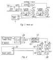
- FIG. 2 A preferred embodiment of the invention is shown in Figure 2.
- the Transmit/Receive (Tx/Rx) Multiplexed parts of the Radio Frequency (RF) module which are necessary to describe the invention are shown.
- Channel 1 consists of antenna 1,10, capacitor 14, and transistor is.
- Channel 2 consists of antenna 2,12, capacitor 16, and transistor 20. Each channel is connected to a different port of logic circuit 22. In addition, both channels are connected to the resonant circuit 24 of the transmitter stage.
- transistor 20 is conducting via the parasitic diode across the drain to source pins of transistor 20. Due to the parasitic diode phenomena, effectively, there are two antennas connected in parallel to the antenna resonator 24. This in turn detunes resonator 24 and inhibits antenna resonator's 24 ability to generate the high voltages necessary to charge up the transponder. Without the series capacitors 14,16, the above-mentioned result is effected.
- the capacitor 16 is charged up to the peak voltage of the antenna resonator 24 via the parasitic diode across transistor 20.
- the polarity of the voltage charged onto capacitor 16 is positive with respect to the ground of antenna 2,12 (which is also at the same potential as the source pin of the MOSFET). Therefore, the source pin of transistor 20 is at a positive potential due to the voltage at the antenna resonator 24 plus the positive voltage charged onto capacitor 16 and therefore transistor 20 will not conduct via the parasitic diode.
Abstract
Description
- This invention generally relates to multiple antenna capability in transceiver systems.
- In a standard Radio Frequency-Identification (RF-ID) system, an interrogating antenna, sometimes called the transmitter antenna, transmits a power burst signal of some predetermined duration to power up the passive transponder in the field to respond. Once the transponder is fully charged from the interrogation signal, the power burst signal is damped at the interrogator, and the transponder transmits it response telegram. The response telegram is received by a receive antenna in the interrogation unit and generally consists of identification information and/or sensor or other data. Oftentimes, not only is a single interrogation antenna and a single receive antenna necessary for the operation of any given transceiver system, but more realistically, several receive antennas and perhaps more than one interrogation antenna are necessary for optimal operation of more complex transceiver systems.
- The problems associated with connecting more than one antenna to a single RF Module exist in the particular method used to multiplex the antennas to the RF module or interrogation unit. Generally switches are used to connect the antennas to the RF Module. Due to low power losses and the high reliability associated with power MOS FETs, power MOS FETs are generally the switch of choice. Power MOS FETs, however, have the disadvantage that a parasitic anti-parallel diode exists across the drain to source pins of the FETs while the device is not conducting. The anti-parallel diode is automatically generated in the production of the Power MOS FETs and manifests itself as a P-N junction barrier in the silicon substrate of the MOS FET. The disadvantageous characteristics of the diode are the conducting and non-conducting features of the diode upon proper application of voltage applied across the diode, such that the diodes enhance conduction of the MOS FETs when the MOS FETs are not conducting.
- Current solutions to the diode behavior exhibited by the Power MOS FETs during non-conduction are to connect anti-serial MOS FETs across the drain to source pins of the MOS FETs. Anti-serial connection of the MOSFETS is shown in Figure 1, where the two MOS FETs are connected in series, but the second MOS FET is reversed (anti-serial) such that the order of the MOS FET pins is drain1 - source1 - source2 - drain2. Anti-serial connection of the MOS FETs creates anti-serial connection of the parasitic diodes as well and therefore the cathode of the parasitic diode always appears at the drain pin of the MOS FET, and the anode of the parasitic diode exists at the source pin of the MOS FET, resulting in only one parasitic diode in conduction at a time. However, connecting MOSFETs anti-serial creates the additional requirement of having to use a driver circuit, to operate the gate pin of the power MOSFETs, which is not referenced to ground, or is floating, as shown in Figure 1. This greatly increases the cost of the Multiplexer and transceiver system due to the expensive nature of the floating driver circuit. A floating driver circuit is expensive and not commonly used, because it is not referenced to ground. Unable to reference a signal to ground, the floating driver circuit requires the use of a transformer to galvanically separate the digital control signals from the driver circuit for each channel. The transformer must also withstand high voltages which also makes it more expensive. In conclusion, the additional MOSFETs used to solve the parasitic diode problem, created a much more significant cost and feasibility burden.
- A preferred embodiment of the invention overcomes the disadvantage of the parasitic diode by connecting the power MOS FET to the antenna via a serially connected capacitor. Thus, in a disabled channel, the serially connected capacitor may be charged up to the peak positive D.C. voltage of the antenna resonator circuit of the enabled channel, via the parasitic diode. The capacitor in the disabled channel is charged via the parasitic diode while a different transmit channel has been selected and when the antenna resonator of that different channel, builds up the antenna resonance voltage. Once the voltage at the antenna resonator is at the maximum, the capacitor in the disabled channel is also charged up to the maximum voltage and therefore, the antenna resonance voltage of the enabled channel minus the stored voltage of the disabled channel capacitor will never be less than zero. In conclusion, because the drain of the FET is held to a positive voltage, and the parasitic diode needs a negative voltage to conduct, the parasitic voltage stops conducting and will not conduct while the capacitor is charged to that positive voltage. Therefore, the FET is blocked to negative voltages.
- The disabled MOS FET is also blocked for positive voltages because that is the basic function of the MOS FET switch. The parasitic diode is not conducting in this situation, because the diode is reversed biased in this case and therefore needs a negative voltage to conduct.
- One advantage of this invention is a replacement of the excessive number of expensive additional components previously necessary to solve the parasitic diode problem with fewer significantly less expensive components.
- A second advantage of this configuration is the ease in implementation and facilitation of the new improved solution.
- The invention will be explained in greater detail with reference to an example of an embodiment shown in the drawings, in which:
- Figure 1 is schematic of a multiplex configuration showing the floating gate driver circuit characteristic generated.
- Figure 2 is a schematic of the multiplex configuration according to a preferred embodiment according to the invention.
- A preferred embodiment of the invention is shown in Figure 2. In Figure 2, the Transmit/Receive (Tx/Rx) Multiplexed parts of the Radio Frequency (RF) module which are necessary to describe the invention are shown. A two channel multiplexed is shown.
Channel 1 consists ofantenna capacitor 14, and transistor is.Channel 2 consists ofantenna capacitor 16, andtransistor 20. Each channel is connected to a different port oflogic circuit 22. In addition, both channels are connected to theresonant circuit 24 of the transmitter stage. - In operation, assume that the RF Module's transmitter is now switched on and that
channel 1 of the TX/RX multiplexed is selected i.e. enabled.Transistor 18 is conducting andtransistor 20 is switched off or not conducting. Althoughtransistor 20 is not conducting, the parasitic diode across the drain-source pins oftransistor 20 is present and conducting for negative voltages. Even in more detail, when the RF Module's transmitter is switched on, the first positive sine halfwave is coupled toantenna resonator 24. For the positive half of the sinewave, no problem exists for thenon-conducting transistor 20, because the parasitic diode will only conduct for negative voltages. Therefore, the problem exists upon the coupling of the negative half of the sinewave toantenna resonator 24. During the negative half of the sinewave,transistor 20 is conducting via the parasitic diode across the drain to source pins oftransistor 20. Due to the parasitic diode phenomena, effectively, there are two antennas connected in parallel to theantenna resonator 24. This inturn detunes resonator 24 and inhibits antenna resonator's 24 ability to generate the high voltages necessary to charge up the transponder.
Without theseries capacitors - However, with the
series capacitors channel 1 is selected andtransistor 18 is conducting, thecapacitor 16 is charged up to the peak voltage of theantenna resonator 24 via the parasitic diode acrosstransistor 20. The polarity of the voltage charged ontocapacitor 16 is positive with respect to the ground ofantenna 2,12 (which is also at the same potential as the source pin of the MOSFET). Therefore, the source pin oftransistor 20 is at a positive potential due to the voltage at theantenna resonator 24 plus the positive voltage charged ontocapacitor 16 and thereforetransistor 20 will not conduct via the parasitic diode. - A few preferred embodiments have been described in detail hereinabove. It is to be understood that the scope of the invention also comprehends embodiments different from those described, yet within the scope of the claims.
- While this invention has been described with reference to illustrative embodiments, this description is not intended to be construed in a limiting sense. Various modifications and combinations of the illustrative embodiments, as well as other embodiments of the invention, will be apparent to persons skilled in the art upon reference to the description. It is therefore intended that the appended claims encompass any such modifications or embodiments.
Claims (5)
- A multiplex system for connecting more than one antenna to a transmitter/receiver comprising:
control circuitry for selecting an antenna resonator via enabling and disabling circuitry;
more than one antenna resonator for transmission of a charge-up pulse to a transponder in dependence upon being selected via said control circuitry and upon reaching a maximum resonator voltage;
a transmitter for charging up a selected antenna resonator to said maximum resonator voltage;
a switch circuit, connected to said antenna resonator, for conducting when enabled via said control circuit, and not conducting when disabled via said control circuit;
at least one serially connected capacitor corresponding to each of said switch circuits, for storing substantially said maximum resonator voltage, in dependence upon said corresponding switch circuit being disabled. - The system of Claim 1, wherein said switch circuit is a MOS FET circuit.
- The system of Claim 2, wherein said MOS FET circuitry has a gate and wherein further said control circuit controls the voltage on said gate of said MOS FET circuitry.
- The system of Claim 1, wherein said at least one serially connected capacitor is a parallel combination of two capacitors.
- The system of Claim 1, wherein said at least one serially connected capacitor is connected in between said antenna resonator and said switch circuitry.
Applications Claiming Priority (2)
| Application Number | Priority Date | Filing Date | Title |
|---|---|---|---|
| US36564494A | 1994-12-29 | 1994-12-29 | |
| US365644 | 1994-12-29 |
Publications (2)
| Publication Number | Publication Date |
|---|---|
| EP0724308A2 true EP0724308A2 (en) | 1996-07-31 |
| EP0724308A3 EP0724308A3 (en) | 1998-10-14 |
Family
ID=23439726
Family Applications (1)
| Application Number | Title | Priority Date | Filing Date |
|---|---|---|---|
| EP95120130A Withdrawn EP0724308A3 (en) | 1994-12-29 | 1995-12-20 | Antenna arrangement |
Country Status (2)
| Country | Link |
|---|---|
| EP (1) | EP0724308A3 (en) |
| JP (1) | JPH08320376A (en) |
Cited By (3)
| Publication number | Priority date | Publication date | Assignee | Title |
|---|---|---|---|---|
| EP0740262A2 (en) * | 1995-04-28 | 1996-10-30 | Texas Instruments Deutschland Gmbh | Identification system reader with multiplexed antennas |
| DE102004058613A1 (en) * | 2004-12-04 | 2006-06-08 | Conti Temic Microelectronic Gmbh | Transmitting device for a plurality of mutually parallel, independently supplied via a respective supply line antenna |
| US9774086B2 (en) | 2007-03-02 | 2017-09-26 | Qualcomm Incorporated | Wireless power apparatus and methods |
Families Citing this family (4)
| Publication number | Priority date | Publication date | Assignee | Title |
|---|---|---|---|---|
| US9130602B2 (en) | 2006-01-18 | 2015-09-08 | Qualcomm Incorporated | Method and apparatus for delivering energy to an electrical or electronic device via a wireless link |
| US8447234B2 (en) | 2006-01-18 | 2013-05-21 | Qualcomm Incorporated | Method and system for powering an electronic device via a wireless link |
| US9124120B2 (en) | 2007-06-11 | 2015-09-01 | Qualcomm Incorporated | Wireless power system and proximity effects |
| US9601267B2 (en) | 2013-07-03 | 2017-03-21 | Qualcomm Incorporated | Wireless power transmitter with a plurality of magnetic oscillators |
Citations (7)
| Publication number | Priority date | Publication date | Assignee | Title |
|---|---|---|---|---|
| US4857893A (en) * | 1986-07-18 | 1989-08-15 | Bi Inc. | Single chip transponder device |
| US4987392A (en) * | 1988-10-17 | 1991-01-22 | Motorola, Inc. | Gallium arsenide antenna switch |
| EP0496610A2 (en) * | 1991-01-23 | 1992-07-29 | Texas Instruments Holland B.V. | Interrogating station for identification purposes, with separate transmitting and receiving antennae |
| EP0301127B1 (en) * | 1987-07-31 | 1993-12-01 | Texas Instruments Deutschland Gmbh | Transponder arrangement |
| GB2279212A (en) * | 1993-06-17 | 1994-12-21 | Oki Electric Ind Co Ltd | Antenna switching circuit |
| US5465411A (en) * | 1993-06-16 | 1995-11-07 | Nisshin Onpa Co., Ltd. | Diversity receiver with switching noise reduction |
| EP0740262A2 (en) * | 1995-04-28 | 1996-10-30 | Texas Instruments Deutschland Gmbh | Identification system reader with multiplexed antennas |
-
1995
- 1995-12-20 EP EP95120130A patent/EP0724308A3/en not_active Withdrawn
- 1995-12-27 JP JP7341546A patent/JPH08320376A/en active Pending
Patent Citations (7)
| Publication number | Priority date | Publication date | Assignee | Title |
|---|---|---|---|---|
| US4857893A (en) * | 1986-07-18 | 1989-08-15 | Bi Inc. | Single chip transponder device |
| EP0301127B1 (en) * | 1987-07-31 | 1993-12-01 | Texas Instruments Deutschland Gmbh | Transponder arrangement |
| US4987392A (en) * | 1988-10-17 | 1991-01-22 | Motorola, Inc. | Gallium arsenide antenna switch |
| EP0496610A2 (en) * | 1991-01-23 | 1992-07-29 | Texas Instruments Holland B.V. | Interrogating station for identification purposes, with separate transmitting and receiving antennae |
| US5465411A (en) * | 1993-06-16 | 1995-11-07 | Nisshin Onpa Co., Ltd. | Diversity receiver with switching noise reduction |
| GB2279212A (en) * | 1993-06-17 | 1994-12-21 | Oki Electric Ind Co Ltd | Antenna switching circuit |
| EP0740262A2 (en) * | 1995-04-28 | 1996-10-30 | Texas Instruments Deutschland Gmbh | Identification system reader with multiplexed antennas |
Non-Patent Citations (2)
| Title |
|---|
| MIYATSUJI K ET AL: "A GAAS HIGH-POWER RF SINGLE-POLE DOUBLE-THROW SWITCH IC FOR DIGITALMOBILE COMMUNICATION SYSTEM" IEEE INTERNATIONAL SOLID STATE CIRCUITS CONFERENCE, vol. 37, 1 February 1994, page 34/35, 305 XP000507050 * |
| MOTOKI HIRANO ET AL: "KEYLESS ENTRY SYSTEM WITH RADIO CARD TRANSPONDER" IEEE TRANSACTIONS ON INDUSTRIAL ELECTRONICS, vol. 35, no. 2, 1 May 1988, pages 208-216, XP000096890 * |
Cited By (4)
| Publication number | Priority date | Publication date | Assignee | Title |
|---|---|---|---|---|
| EP0740262A2 (en) * | 1995-04-28 | 1996-10-30 | Texas Instruments Deutschland Gmbh | Identification system reader with multiplexed antennas |
| EP0740262A3 (en) * | 1995-04-28 | 2004-01-02 | Texas Instruments Deutschland Gmbh | Identification system reader with multiplexed antennas |
| DE102004058613A1 (en) * | 2004-12-04 | 2006-06-08 | Conti Temic Microelectronic Gmbh | Transmitting device for a plurality of mutually parallel, independently supplied via a respective supply line antenna |
| US9774086B2 (en) | 2007-03-02 | 2017-09-26 | Qualcomm Incorporated | Wireless power apparatus and methods |
Also Published As
| Publication number | Publication date |
|---|---|
| JPH08320376A (en) | 1996-12-03 |
| EP0724308A3 (en) | 1998-10-14 |
Similar Documents
| Publication | Publication Date | Title |
|---|---|---|
| US6239675B1 (en) | Tuning circuit having switchable capacitor controlled by a selection circuit | |
| US8476961B2 (en) | System and method of transistor switch biasing in a high power semiconductor switch | |
| US6693498B1 (en) | SPDT switch and communication unit using the same | |
| KR100306306B1 (en) | Telecommunication device | |
| US20070008132A1 (en) | Switchable directional coupler for use with RF devices | |
| US20100290368A1 (en) | Half-duplex rfid transponder and a method of operating a half-duplex rfid transponder | |
| US6218819B1 (en) | Voltage regulation device having a differential amplifier coupled to a switching transistor | |
| US9048840B2 (en) | 20V to 250V high current ASIC PIN diode driver | |
| US4525863A (en) | Solid state transmit/receive switch | |
| EP2438551A1 (en) | Switching radio frequency identification (rfid) tags | |
| US11050238B2 (en) | Electronic circuit for providing protection for an energy supply for a receiving device | |
| EP0724308A2 (en) | Antenna arrangement | |
| US5563589A (en) | Remote identification device | |
| US4979232A (en) | Self-biasing solid-state T/R switch | |
| US20040259505A1 (en) | Switch circuit especially suitable for use in wireless LAN applications | |
| US6262903B1 (en) | Direct-current power supply circuit having control sections with at least one control section having priority over another control section | |
| WO2018044489A9 (en) | Transmitting and receiving device and ultrasonic system | |
| US5642059A (en) | Bus driver circuit with overvoltage protection | |
| US8328105B2 (en) | Semiconductor device | |
| WO1995013668A1 (en) | Electronic antenna switching system | |
| CA2312974A1 (en) | Active transponder switchable into passive transponder | |
| US5737165A (en) | Apparatus for databus fault isolation | |
| US10305376B1 (en) | Switchable charge pump for multi-mode operation | |
| US6066974A (en) | High power transistor switch with low transmission loss | |
| CN212811546U (en) | Chip control conversion circuit |
Legal Events
| Date | Code | Title | Description |
|---|---|---|---|
| PUAI | Public reference made under article 153(3) epc to a published international application that has entered the european phase |
Free format text: ORIGINAL CODE: 0009012 |
|
| AK | Designated contracting states |
Kind code of ref document: A2 Designated state(s): DE FR GB IT NL |
|
| RIN1 | Information on inventor provided before grant (corrected) |
Inventor name: FLAXL, THOMAS JOSEF |
|
| RAP1 | Party data changed (applicant data changed or rights of an application transferred) |
Owner name: TEXAS INSTRUMENTS DEUTSCHLAND GMBH |
|
| PUAL | Search report despatched |
Free format text: ORIGINAL CODE: 0009013 |
|
| AK | Designated contracting states |
Kind code of ref document: A3 Designated state(s): DE FR GB IT NL |
|
| 17P | Request for examination filed |
Effective date: 19990407 |
|
| 17Q | First examination report despatched |
Effective date: 20030721 |
|
| STAA | Information on the status of an ep patent application or granted ep patent |
Free format text: STATUS: THE APPLICATION IS DEEMED TO BE WITHDRAWN |
|
| 18D | Application deemed to be withdrawn |
Effective date: 20040203 |