EP0741370B2 - Method for applying a security element on a substrate - Google Patents
Method for applying a security element on a substrate Download PDFInfo
- Publication number
- EP0741370B2 EP0741370B2 EP95810302A EP95810302A EP0741370B2 EP 0741370 B2 EP0741370 B2 EP 0741370B2 EP 95810302 A EP95810302 A EP 95810302A EP 95810302 A EP95810302 A EP 95810302A EP 0741370 B2 EP0741370 B2 EP 0741370B2
- Authority
- EP
- European Patent Office
- Prior art keywords
- substrate
- layer
- laminate
- adhesive layer
- security element
- Prior art date
- Legal status (The legal status is an assumption and is not a legal conclusion. Google has not performed a legal analysis and makes no representation as to the accuracy of the status listed.)
- Expired - Lifetime
Links
Images


Classifications
-
- B—PERFORMING OPERATIONS; TRANSPORTING
- B42—BOOKBINDING; ALBUMS; FILES; SPECIAL PRINTED MATTER
- B42D—BOOKS; BOOK COVERS; LOOSE LEAVES; PRINTED MATTER CHARACTERISED BY IDENTIFICATION OR SECURITY FEATURES; PRINTED MATTER OF SPECIAL FORMAT OR STYLE NOT OTHERWISE PROVIDED FOR; DEVICES FOR USE THEREWITH AND NOT OTHERWISE PROVIDED FOR; MOVABLE-STRIP WRITING OR READING APPARATUS
- B42D25/00—Information-bearing cards or sheet-like structures characterised by identification or security features; Manufacture thereof
- B42D25/40—Manufacture
- B42D25/45—Associating two or more layers
- B42D25/465—Associating two or more layers using chemicals or adhesives
- B42D25/47—Associating two or more layers using chemicals or adhesives using adhesives
-
- B—PERFORMING OPERATIONS; TRANSPORTING
- B42—BOOKBINDING; ALBUMS; FILES; SPECIAL PRINTED MATTER
- B42D—BOOKS; BOOK COVERS; LOOSE LEAVES; PRINTED MATTER CHARACTERISED BY IDENTIFICATION OR SECURITY FEATURES; PRINTED MATTER OF SPECIAL FORMAT OR STYLE NOT OTHERWISE PROVIDED FOR; DEVICES FOR USE THEREWITH AND NOT OTHERWISE PROVIDED FOR; MOVABLE-STRIP WRITING OR READING APPARATUS
- B42D25/00—Information-bearing cards or sheet-like structures characterised by identification or security features; Manufacture thereof
- B42D25/20—Information-bearing cards or sheet-like structures characterised by identification or security features; Manufacture thereof characterised by a particular use or purpose
- B42D25/29—Securities; Bank notes
-
- B—PERFORMING OPERATIONS; TRANSPORTING
- B42—BOOKBINDING; ALBUMS; FILES; SPECIAL PRINTED MATTER
- B42D—BOOKS; BOOK COVERS; LOOSE LEAVES; PRINTED MATTER CHARACTERISED BY IDENTIFICATION OR SECURITY FEATURES; PRINTED MATTER OF SPECIAL FORMAT OR STYLE NOT OTHERWISE PROVIDED FOR; DEVICES FOR USE THEREWITH AND NOT OTHERWISE PROVIDED FOR; MOVABLE-STRIP WRITING OR READING APPARATUS
- B42D25/00—Information-bearing cards or sheet-like structures characterised by identification or security features; Manufacture thereof
- B42D25/30—Identification or security features, e.g. for preventing forgery
- B42D25/328—Diffraction gratings; Holograms
-
- B—PERFORMING OPERATIONS; TRANSPORTING
- B42—BOOKBINDING; ALBUMS; FILES; SPECIAL PRINTED MATTER
- B42D—BOOKS; BOOK COVERS; LOOSE LEAVES; PRINTED MATTER CHARACTERISED BY IDENTIFICATION OR SECURITY FEATURES; PRINTED MATTER OF SPECIAL FORMAT OR STYLE NOT OTHERWISE PROVIDED FOR; DEVICES FOR USE THEREWITH AND NOT OTHERWISE PROVIDED FOR; MOVABLE-STRIP WRITING OR READING APPARATUS
- B42D25/00—Information-bearing cards or sheet-like structures characterised by identification or security features; Manufacture thereof
- B42D25/40—Manufacture
- B42D25/45—Associating two or more layers
- B42D25/455—Associating two or more layers using heat
-
- G—PHYSICS
- G06—COMPUTING; CALCULATING OR COUNTING
- G06K—GRAPHICAL DATA READING; PRESENTATION OF DATA; RECORD CARRIERS; HANDLING RECORD CARRIERS
- G06K19/00—Record carriers for use with machines and with at least a part designed to carry digital markings
- G06K19/06—Record carriers for use with machines and with at least a part designed to carry digital markings characterised by the kind of the digital marking, e.g. shape, nature, code
- G06K19/06009—Record carriers for use with machines and with at least a part designed to carry digital markings characterised by the kind of the digital marking, e.g. shape, nature, code with optically detectable marking
- G06K19/06046—Constructional details
-
- B42D2033/04—
-
- B42D2035/20—
Definitions
- EP 401 466 is a security element designed as a layered composite known for sticking on a document.
- the layer composite has diffraction structures that between a stabilization layer and a thermal activatable adhesive layer are embedded.
- the transfer of the layered group on the document, by the adhesive layer through the layer composite heat is supplied therethrough, the stabilization layer the heat evenly distributed and one locally excessive heating of the diffraction structures bearing layers of paint prevented.
- the layer composite serves because of its diffraction structures caused optical effects as a security element.
- hot stamping is the Application of a relatively high pressure and sufficient heating required what with security elements that have optical diffraction structure or interference effects, without impairing these security elements not without further is possible.
- the lacquer layer 3 can also directly be applied to the backing layer 1 if the adhesiveness the lacquer layer 3 on the carrier layer 1 is sufficient.
- Adhesion can advantageously be by means of a Pretreatment of the carrier layer 1, e.g. B. in a corona or plasma discharge. A boundary layer between the lacquer layer 3 and the carrier layer 1 or one modified by the pretreatment Surface layer of the film takes over in these examples the function of the intermediate layer 2.
- the lacquer layer 3 can be applied directly be applied to the backing layer 1 if the adhesiveness the lacquer layer 3 on the carrier layer 1 so is agreed that after connecting the layer composite 7 with the substrate 9 on the carrier layer 1 those points of the layer composite 7 that on adhere to the substrate 9, easily from the paint layer 3 can be separated and that the carrier layer 1 at those points in the layer composite 7 that are not adhere to the substrate 9, the layers 3, 4, 5, 6 of the Layer composite 7 pulls, the layers 3, 4, 5, 6 along the border between the adhesive and the non-adhesive areas of the layer composite 7 tear.
- the first lacquer layer 3 is advantageous in at least applied in one operation and typically has one Layer thickness between 0.5 and 3.0 micrometers, preferably 1.5 microns.
- the relief of the diffraction structures 8 has a typical one Profile height that ranges from about 0.1 to 1.5 microns, while the grid spacing of the Diffraction structures 8 is about 0.1 to 10 microns.
- An application of the second lacquer layer 5 of about 0.15 to 1.5 micron thickness (e.g. 1 micron) levels the relief completely. It is advantageous for both layers of paint 3 and 5 uses the same material, for example a thermoplastic acrylic polymer paint.
- the second lacquer layer 5 serves primarily as an adhesion promoter between the reflective layer 4 and the adhesive layer 6. If necessary, they can be dispensed with become.
- the acrylic polymer lacquer of the lacquer layer 3 can do so be colored such that they are at least in a predetermined Part of the light spectrum is transparent.
- the Diffraction structure 8 remains in a predetermined wavelength range can be read out mechanically or visually. Is for example the dye for infrared light only permeable, the diffraction structure 8 is the unarmed Eye hidden and only by means of one not here shown reader recognizable that the presence the diffraction structure 8 is able to determine.
- the finished layer composite 7 leaves the Rewinding system, for example in the form of a roll, the graphic compositions from diffraction structures 8 which optical effects of the above Kind of effect.
- the detection system 14 can also be set up for this be the exact location of on the laminate 7 existing partial areas with diffraction structures Represent 8 provided elements to determine so that selected, well-defined elements of the layer composite 7 can be transferred to the substrate 9 are.
- the positioning is preferably carried out in y direction by shifting a single roll of the Rewinding system, because the inertia of the film tape is very is low.
- the shift of a single role is enough because with correct basic setting of the system only small displacements are necessary that the foil tape don't warp.
- the adhesive layer After the adhesive layer has cooled 6 will be the carrier film in a next step 1, 2 subtracted.
- the intermediate layer comes off 2 of the lacquer layer 3 at those points of the layer composite 7, which has previously been sufficiently heated were and thus adhere to the substrate 9.
- the intermediate layer 2 On the non-adhesive areas of the adhesive layer on the substrate 9 6, the intermediate layer 2 does not separate the lacquer layer 3 and the layers 3, 4, 5, 6 tear along the border between the sticky and the non-adhesive areas so that layers 3, 4, 5, 6 at the adhesive points of the layer composite 7 the substrate 9 remain.
- the use of the guided laser beam 12 enables further an application of the Layer composite 7 on the substrate 9 in two ways.
- the detection system 14 (Fig. 2) the location of, for example, on the Substrate 9 printed patterns with high accuracy to determine and then the laser beam 12 according to the location of these patterns that after peeling off the backing sheet on the substrate 9 remaining parts of the layer composite 7 in register to which patterns are aligned.
- a guilloche on a document to apply, of which individual lines are printed and individual Lines as layer composite 7 with diffraction structures 8 are glued on.
- Another option is there in it, parts of a graphic element, a character or a number, etc. with printing ink and the the element, the character or the Additional parts in register in the form of a transferred layer composite 7 with diffraction structures 8 to train.
- This combination of different Technologies result in a high level of security against Counterfeiting and manipulation.
- a security element it is possible as a security element to provide a layered composite 7 which is a predetermined one Design of elements such as Lines, pixels, Points, surface elements, etc., the special Diffraction structures 8 contained in their interaction for example create an optical effect, as from products sold under the brand name KINEGRAM® are sold, are known.
- the detection system 14 is now, as described above, set up to recognize the location of this design so the laser beam 12 is exactly over the elements of this design can be done. After peeling off the carrier film then this design remains on the Substrate 9 back. With this technology you can on the one hand, fine details such as very narrow lines the layer composite 7 transferred to the substrate 9.
- Reflective layer 4 there is a layer composite 7 with a highly reflective one Reflective layer 4 can be used, which is a high brilliance of the transmitted diffraction structures 8 guaranteed.
- an optical security element like a KINEGRAM® occupied area with diffraction structures 8 provided.
- the rest of the surface is optically diffraction not active and can in particular like a mirror Act.
- the substrate 9 is also within the assigned to the optical security element Area only partially covered. Thanks to the strong reflective reflection layer 4 appears the diffraction optical Security element nevertheless in high Brilliance.
- the method with the controlled laser beam 12 is particularly suitable for accurate application a security element to counterfeiting protective document, such as a banknote.
- the 8 and 9 show in plan view and in cross section a banknote 37 with patterns 38 and with a continuous Number 39 is printed and a security element 40, which represents the same number 39.
- the banknote has lines 41 which are made of Sub-lines 42 and 43 of a first and a second type are composed.
- the sub-lines 42 and 43 are in 8 drawn or drawn in dashed lines.
- the control device detects by means of of the detection system 14 the exact xy position of the Banknote 37 and the value of number 39.
- the security element 40 is made from a layer composite 7 (Fig.
- a locally limited or a full area for visible Transparent protective layer 44 e.g. from a UV curable varnish to apply to the diffractive Line elements of number 40 and lines 41 protect against mechanical abrasion.
Abstract
Description
Die Erfindung betrifft ein Verfahren zum Aufbringen und Individualisieren oder Personalisieren eines Sicherheitselementes auf ein Substrat oder Dokument gemäss dem Oberbegriff des Anspruchs 1.The invention relates to a method for application and individualizing or personalizing a security element according to a substrate or document the preamble of claim 1.
Individualisierte, unveränderbare Sicherheitselemente dienen dem Schutz des damit versehenen Dokumentes gegen unerlaubtes Kopieren, gegen Fälschungen oder unerlaubte Veränderungen des Dokumentes.Individualized, unchangeable security elements serve to protect the document provided with it against unauthorized copying, against counterfeiting or unauthorized changes to the document.
Aus der europäischen Patentanmeldung EP 401 466 ist ein als Schichtverbund ausgebildetes Sicherheitselement zum Aufkleben auf ein Dokument bekannt. Der Schichtverbund weist Beugungsstrukturen auf, die zwischen eine Stabilisationsschicht und eine thermisch aktivierbare Kleberschicht eingebettet sind. Die Übertragung des Schichtverbundes auf das Dokument erfolgt, indem der Kleberschicht durch den Schichtverbund hindurch Wärme zugeführt wird, wobei die Stabilisationsschicht die Wärme gleichmässig verteilt und eine lokal übermässige Erhitzung der die Beugungsstrukturen tragenden Lackschichten verhindert. Der Schichtverbund dient wegen seiner durch die Beugungsstrukturen bewirkten optischen Effekte als Sicherheitselement.From European patent application EP 401 466 is a security element designed as a layered composite known for sticking on a document. The layer composite has diffraction structures that between a stabilization layer and a thermal activatable adhesive layer are embedded. The transfer of the layered group on the document, by the adhesive layer through the layer composite heat is supplied therethrough, the stabilization layer the heat evenly distributed and one locally excessive heating of the diffraction structures bearing layers of paint prevented. The layer composite serves because of its diffraction structures caused optical effects as a security element.
Die EP 401 466 offenbart weiter die Ausbildung von gut und schlecht haftenden Stellen auf der Kleberschicht. Bei der thermischen Aktivierung bildet sich nur an den gut haftenden Stellen eine Haftverbindung zwischen dem Schichtverbund und dem Dokument aus. Beim Versuch der Ablösung vom Dokument wird einerseits das Sicherheitselement zerstört. Andererseits bleiben entsprechend dem Muster der Haftbrücken Teile des Sicherheitselementes auf dem Dokument zurück. Das zurückbleibende Muster kann ein sinnergebendes Muster sein und beispielsweise das Wort "VOID" darstellen.EP 401 466 further discloses the formation of good and badly adhering areas on the adhesive layer. Thermal activation only forms an adhesive connection between the well adhering points the shift network and the document. When trying to detach from the document, on the one hand the security element is destroyed. On the other hand, stay according to the pattern of the adhesive bridges parts of the security element on the document. The remaining pattern can be meaningful Be a pattern and represent, for example, the word "VOID".
Die PCT Anmeldung WO 93/16888 offenbart ein Druckverfahren zur Ausbildung der Kleberschicht eines Schichtverbundes mit gut und schlecht haftenden Stellen. Nach der Übertragung des Schichtverbundes auf das Dokument wird die Trägerfolie wieder abgezogen, wobei sich die Trägerfolie an den auf dem Dokument gut haftenden Stellen des Schichtverbundes vom Schichtverbund löst, während sich an den schlecht haftenden Stellen der ganze Schichtverbund vom Dokument löst. Die auf dem Dokument zurückbleibenden Teile des Schichtverbundes sind teilweise fein strukturierte Gebilde und können nicht vom Dokument entfernt werden, ohne sichtbare Spuren zu hinterlassen. Solche Teile können z.B. als feine Linien auf einem Foto vorhanden sein, so dass das Foto zwischen den das Sicherheitselement darstellenden Teilen gut sichtbar ist.PCT application WO 93/16888 discloses a Printing process for forming the adhesive layer Layered composite with good and badly adhering areas. After transfer of the layer composite to the document is peeled off again the backing film adhering to the on the document well adhering parts of the layer composite from Layered composite detaches while adhering to the poorly adhering Make the whole layer composite of the document solves. The parts remaining on the document of the layer composite are partially finely structured Structures and cannot be removed from the document without leaving any visible traces. Such parts can e.g. present as fine lines on a photo be so the photo between the the security element performing parts is clearly visible.
Aus dem japanischen Patent Abstract Vol. 15, No. 362 (M-1157) ist ein Verfahren bekannt, bei dem eine thermoplastische Folie als kratzfeste Schutzschicht auf eine Chipkarte aufgebracht wird. Um ein späteres Abschälen der Folie zu verhindern, wird die mit einer Kleberschicht versehene Oberfläche der Chipkarte an kritischen Stellen mittels eines die Folie durchdringenden Laserstrahles soweit erwärmt, dass die Chipkarte, die Kleberschicht und die Folie miteinander verschweissen.From Japanese Patent Abstract Vol. 15, No. 362 (M-1157) a method is known in which a thermoplastic film as a scratch-resistant protective layer a chip card is applied. For a later peeling To prevent the film, use a layer of adhesive provided surface of the chip card at critical By means of a penetrating film Laser beam heated so far that the chip card, the Weld the adhesive layer and the film together.
Ferner ist es bekannt ("Heißprägen -ein modernes Verfahren für
das Dekorieren von Kunststoff-Teilen" in Kunststoffe 72 (1982)
11 Seiten 701 bis 707 und ICI-Firmendruckschrift "Melinex
Polyesterfilm: Metalizing 1986, Seiten 5, 6 und 8), eine
Prägefolie bestehend aus einer Trägerfolie, einer Trennschicht,
einem Schutzlack, einer als Dekor wirkenden Metallisierung
sowie einer Klebeschicht durch einen heißen Prägestempel
unter relativ hohem Druck soweit zu erhitzen, daß die erhitzten
Flächen von nicht erhitzten Teilen der Schichten ge-wissermaßen
ausgestanzt und mittels der erwärmten Klebeschicht
an eine Kunststoffunterlage angeklebt werden, die jedenfalls
oberflächlich plastifiziert wurde. Bei diesem für andere
Zwecke des Dekorierens von Kunststoffartikeln, wie Tuben,
Dosen, Flaschen oder dergleichen, dienenden Heißprägen ist die
Anwendung eines relativ hohen Drucks und ausreichender Erhitzung
erforderlich, was bei Sicherheitselementen, die
optische Beugungsstruktur oder Interferenzeffekte aufweisen,
ohne Beeinträchtigung dieser Sicherheitselemente nicht ohne
weiteres möglich ist.It is also known ("hot stamping - a modern process for
Decorating Plastic Parts "in Plastics 72 (1982)
11 pages 701 to 707 and ICI company publication "Melinex
Polyester film: Metalizing 1986,
Schließlich ist es bekannt (DE-A-2 556 414 und US-A-4 911 302) Wärme- oder Laserstrahlen zum Bedrucken eines Trägers, der mit einem Farbband versehen ist, und zum Verdampfen von Druckfarbe zu verwenden.Finally, it is known (DE-A-2 556 414 and US-A-4 911 302) Heat or laser beams for printing on a carrier with is provided with a ribbon, and for evaporating printing ink to use.
Der Erfindung liegt die Aufgabe zugrunde, das Verfahren der eingangs genannten Gattung dahingehend zu verbessern, daß auch sehr fein strukturierte Muster des Sicherheitselements einfach, zuverlässig und bei Bedarf auch registergenau auf dem Substrat herstellbar sind, was auch das Individualisieren und/oder Personalisieren von Dokumenten erlaubt.The invention has for its object the method of improve the genus mentioned in that very finely structured pattern of the security element simple, reliable and if necessary also accurate on the register Substrate can be produced, which also means individualizing and / or personalization of documents allowed.
Die Erfindung ist in den Patentansprüchen 1-3 gekennzeichnet und in Unteransprüchen sind weitere Verbesserungen beansprucht.The invention is characterized in the claims 1-3 and further improvements are in subclaims claimed.
Nachfolgend werden Ausführungsbeispiele der Erfindung anhand der Zeichnung näher erläutert.The following are exemplary embodiments of the invention explained in more detail with reference to the drawing.
Es zeigen:
- Fig. 1
- einen auf ein Substrat geklebten Schichtverbund im Querschnitt,
- Fig. 2
- eine Einrichtung zum Aufkleben des Schichtverbundes auf das Substrat,
- Fig. 3
- eine zweite Einrichtung zum Aufkleben des Schichtverbundes auf das Substrat,
- Fig. 4
- eine dritte Einrichtung zum Aufkleben des Schichtverbundes auf das Substrat,
- Fig. 5
- einen Ausweis mit Sicherheitselementen,
- Fig. 6
- eine Ziffer in Mikroschrift,
- Fig. 7
- einen Check,
- Fig. 8, 9
- eine Banknote und
- Fig. 10
- einen weiteren Schichtverbund.
- Fig. 1
- a cross-section of a laminate bonded to a substrate,
- Fig. 2
- a device for gluing the layered composite onto the substrate,
- Fig. 3
- a second device for adhering the layer composite to the substrate,
- Fig. 4
- a third device for adhering the layer composite to the substrate,
- Fig. 5
- an ID card with security elements,
- Fig. 6
- a digit in micro script,
- Fig. 7
- a check,
- 8, 9
- a banknote and
- Fig. 10
- another layer composite.
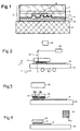
In der Figur 1 bedeutet 1 eine Trägerschicht, auf der
in der angegebenen Reihenfolge eine Zwischenschicht
2, eine erste Lackschicht 3, eine reflektierende Reflexionsschicht
4, eine zweite Lackschicht 5 und eine Kleberschicht
6 aufgebracht sind. Die Schichten 1 bis 6 bilden
einen Schichtverbund 7. Zwischen den Lackschichten
3 und 5 sind optische Beugungsstrukturen 8 eingebettet,
z. B. Gitter, Hologramme, oder Beugungsstrukturen,
wie sie aus der europäischen Patentschrift EP
105 099 bekannt sind, usw., welche durch die Lackschicht
3 hindurch auftreffendes Licht beugen und mindestens
teilweise reflektieren. Der Schichtverbund 7
wird mittels eines später näher erläuterten Verfahrens
an vorbestimmten Stellen mit einem Substrat 9 verklebt,
wobei die Kleberschicht 6 auf dem Substrat 9 aufliegt.In FIG. 1, 1 means a carrier layer on which
an intermediate layer in the order given
2, a
Die Beugungstrukturen 8 sind mikroskopisch feine
Reliefstrukturen, deren geometrische Parameter Linienabstand,
Orientierung und Profilform örtlich in einer
vorbestimmten Art und Weise derart variieren, dass sie
bei Betrachtung und Bewegung des Substrats 9 unter
normalen Beleuchtungsverhältnissen auffällige wechselnde
beugungsoptische Effekte hervorbringen, wie z.
B. unterschiedliche Farbeffekte oder Wechsel zwischen
hell und dunkel. Ein weiterer optischer Effekt kann darin
bestehen, dass benachbarte Flächenelemente in unterschiedlicher
Helligkeit oder unterschiedlicher Farbe
sichtbar sind, wobei beim Drehen oder Kippen des Substrats
9 die relative Helligkeit oder Farbe der Flächenelemente
ändert. Die Beugungsstrukturen 8 können insbesondere
die wechselnden optischen Effekte erzeugen,
wie sie von Hologrammen oder von Optical Variable
Devices, wie sie beispielsweise in der europäischen
Patentschrift EP 375 833 beschrieben sind, bekannt
sind. Die optischen Effekte der Beugungsstrukturen 8
stellen ein visuell einfach überprüfbares Merkmal dar.The
Für die Trägerschicht 1 ist beispielsweise eine Folie
aus Polyester sehr geeignet, da sich Polyesterfolien
durch hohe Zugfestigkeit und hohe Temperaturbeständigkeit
auszeichnen. Solche Folien sind auf Rollen in
verschiedener Dicke handelsüblich, so dass mit Vorteil,
wie weiter unten ausgeführt, mittels einer hier nicht gezeigten
Umrollanlage auf einer Seite der Trägerschicht
1 der Schichtverbund 7 aufgebaut wird. Vorteilhaft weist
die Trägerschicht 1 eine Dicke von wenigstens 6 Mikrometer
auf, damit sie genügend reissfest ist. Bevorzugt
ist eine Dicke von 20 µm. Bei bestimmten Anwendungen
erreicht die Dicke jedoch ohne weiteres 50 µm. Die Trägerschicht
1 und, falls vorhanden, die Zwischenschicht
2 bilden eine Trägerfolie.A film is, for example, for the carrier layer 1
made of polyester very suitable because there are polyester films
due to high tensile strength and high temperature resistance
award. Such slides are on rolls in
of different thicknesses commercially available, so with advantage
as explained below, by means of a not shown here
Rewinding system on one side of the carrier layer
1 the
Falls es erforderlich ist, dass sich die Trägerschicht
1 und die Zwischenschicht 2 in einem späteren Prozessschritt
leicht von der Lackschicht 3 lösen, ist die
Zwischenschicht 2 beispielsweise eine ganzflächig auf
der Trägerschicht 1 aufgebrachte Wachsschicht mit einer
Auftragsdicke von vorzugsweise 0.1 Mikrometern.
Falls die Trägerschicht 1 und die Zwischenschicht 2
später nicht vom Rest des Schichtverbundes 7 getrennt
werden sollen, dient ein Haftvermittler (Primer) mit einer
Auftragsdicke im Mikrometerbereich, vorzugsweise im
Bereich von 0.8 bis 2 Mikrometern, als Zwischenschicht
2. Der Haftvermittler bewirkt ein hohes Haftvermögen
zwischen der Trägerschicht 1 und der nachfolgenden
Lackschicht 3. Als Haftvermittler dient vorteilhaft ein
Lack auf der Basis von Polyurethan, damit die Zwischenschicht
2 gegen Licht, vorallem gegen ultraviolettes
Licht, und gegen Lösungsmittel beständig ist.If it is necessary that the backing layer
1 and the
Im letzteren Fall kann die Lackschicht 3 auch direkt
auf die Trägerschicht 1 aufgetragen sein, falls das Haftvermögen
der Lackschicht 3 auf der Trägerschicht 1 genügt.
Vorteilhaft kann das Haftvermögen mittels einer
Vorbehandlung der Trägerschicht 1, z. B. in einer Korona
oder Plasmaentladung, erhöht werden. Eine Grenzschicht
zwischen der Lackschicht 3 und der Trägerschicht
1 bzw. eine durch die Vorbehandlung veränderte
Oberflächenschicht der Folie übernimmt in diesen Beispielen
die Funktion der Zwischenschicht 2.In the latter case, the
Auch im ersten Fall kann die Lackschicht 3 direkt
auf die Trägerschicht 1 aufgetragen sein, falls das Haftvermögen
der Lackschicht 3 auf der Trägerschicht 1 so
abgestimmt ist, dass nach dem Verbinden des Schichtverbundes
7 mit dem Substrat 9 die Trägerschicht 1 an
denjenigen Stellen des Schichtverbundes 7, die auf
dem Substrat 9 haften, problemlos von der Lackschicht
3 getrennt werden kann und dass die Trägerschicht 1
an denjenigen Stellen des Schichtverbundes 7, die nicht
auf dem Substrat 9 haften, die Schichten 3, 4, 5, 6 des
Schichtverbundes 7 mitzieht, wobei die Schichten 3, 4,
5, 6 entlang der Grenze zwischen den haftenden und
den nicht haftenden Stellen des Schichtverbundes 7
reissen.In the first case too, the
Vorteilhaft sind für die Trägerschicht 1 gegebenenfalls
Folien verwendbar, die bereits beim Lieferanten mit
der Zwischenschicht 2 überzogen wurden.The carrier layer 1 may be advantageous
Foils can be used that are already with the supplier
the
Die erste Lackschicht 3 ist vorteilhaft in mindestens
einem Arbeitsgang aufgetragen und weist typisch eine
Schichtdicke zwischen 0.5 und 3.0 Mikrometer, vorzugsweise
1.5 Mikrometer, auf.The
Die Beugungsstrukturen 8 werden beispielsweise
mittels einer geheizten Prägematrize als mikroskopisch
feine Reliefstrukturen in die Lackschicht 3 eingeprägt,
wobei die Lackschicht 3 in diesem Fall aus thermoplastischem
Werkstoff besteht. Ein solches Prägeverfahren
ist z.B. aus der schweizerischen Patentschrift 661
683 bekannt. Bei einem weiteren Verfahren, wie es aus
den US-amerikanischen Patentschriften 4 758 296 und
4 840 757 bekannt ist, werden die Beugungsstrukturen
8 durch Abformen in die Lackschicht 3 eingebracht, wobei
die Lackschicht 3 aus UV-härtbarem Lack besteht.The
Anschliessend wird die Reflexionschicht 4 auf die
Lackschicht 3 aufgebracht, die mit Vorteil mittels einer
Koronaentladung vorbehandelt ist, um eine gute Haftung
der Reflexionsschicht 4 auf der Lackschicht 3 zu
bewirken. Vorzugsweise ist als Reflexionsschicht 4 ein
Metall aufgedampft, beispielsweise Aluminium, das kostengünstig
ist und sichtbares sowie infrarotes Licht
schon in dünnen Schichten gut reflektiert. Vorteilhaft
eignet sich auch ein Dielektrikum als Reflexionsschicht
4, mit einem Brechungsindex, der möglicht stark von
den benachbarten Schichten 3 und 5 abweicht, so dass
die Beugungsstrukturen 8 teilweise transparent sind
und darunter liegende Materialien, z. B. ein Bild, nicht
vollständig verdecken.Then the
Es ist auch möglich, die Beugungsstruktur 8 in die
Lackschicht 3 einzuprägen, nachdem die Reflexionsschicht
4 aufgebracht wurde.It is also possible to use the
Das Relief der Beugungsstrukturen 8 weist eine typische
Profilhöhe auf, die im Bereich von etwa 0.1 bis
1.5 Mikrometer liegt, während der Gitterabstand der
Beugungsstrukturen 8 etwa 0.1 bis 10 Mikrometer beträgt.
Ein Auftrag der zweiten Lackschicht 5 von etwa
0.15 bis 1.5 Mikrometer Dicke (z. B. 1 Mikrometer) ebnet
das Relief völlig ein. Mit Vorteil wird für beide Lackschichten
3 und 5 das gleiche Material verwendet, beispielsweise
ein thermoplastischer Acrylpolymerlack.
Die zweite Lackschicht 5 dient vorwiegend als Haftvermittler
zwischen der Reflexionsschicht 4 und der Kleberschicht
6. Auf sie kann gegebenenfalls verzichtet
werden.The relief of the
Der Acrylpolymerlack der Lackschicht 3 kann so
eingefärbt werden, dass sie wenigstens in einem vorbestimmten
Teil des Lichtspektrums transparent ist. Die
Beugungsstruktur 8 bleibt in einem vorbestimmten Wellenlängenbereich
maschinell oder visuell auslesbar. Ist
beispielsweise der Farbstoff nur für infrarotes Licht
durchlässig, ist die Beugungsstruktur 8 dem unbewaffneten
Auge verborgen und nur mittels eines hier nicht
gezeigten Lesegerätes erkennbar, das die Anwesenheit
der Beugungsstruktur 8 festzustellen vermag.The acrylic polymer lacquer of the
Die abschliessend aufgebrachte Kleberschicht 6
von typisch weniger als 6 Mikrometer Dicke ermöglicht
das Aufkleben des Schichtverbundes 7 auf das Substrat
9. Die Schichtdicke der Kleberschicht 6 ist vorteilhaft der
Oberflächenbeschaffenheit des Substrates 9 angepasst.
Bei glatten Substraten 9, wie z. B. bei Photopapieren,
reichen 3 Mikrometer Dicke der Kleberschicht 6
aus, während die Kleberschicht 6 bei einem rauhen
Substrat 9 mit Vorteil eine Dicke von 6 Mikrometern oder
mehr aufweist. Bei einem Papier mit einer normalen
Oberflächenstruktur beispielsweise beträgt die Dicke
der Kleberschicht 6 etwa 5 Mikrometer.The finally applied
Für die Kleberschicht 6 sind mit Wärme aktivierbare
Heisskleber vorgesehen, z. B. auf der Basis von Polymethylmethacrylat,
die beim Erwärmen ab etwa 80°C
ihre Klebkraft entwickeln. Der Schichtverbund 7 kann jedoch
erst bei einer Temperatur des Heissklebers von
mehr als 170°C wieder vom Substrat 9 gelöst werden,
ohne dass im Schichtverbund 7 zu grosse, die Schichten
3 bis 5 zerstörende Zugkräfte auftreten.For the
Der fertiggestellte Schichtverbund 7 verlässt die
Umrollanlage beispielsweise in Form einer Rolle, die
graphische Kompositionen aus Beugungsstrukturen 8
aufweist, welche optische Effekte der oben genannten
Art bewirken.The
Die Fig. 2 zeigt in nichtmassstäblicher Zeichnung in
der xz-Ebene eine Einrichtung zum Aufkleben des
Schichtverbundes 7 auf das Substrat 9. Das Substrat 9
liegt in einer dazu senkrechten xy-Ebene auf einer ebenen
Platte 10 auf. Mittels einer zweiten Platte 11 wird
der Schichtverbund 7 gegen das Substrat 9 und die Platte
10 gepresst, so dass der Schichtverbund 7 in direktem
Kontakt gleichmässig auf dem Substrat 9 aufliegt.
Der von einer Steuereinrichtung, z.B. einem Computer,
gesteuerte Lichtstrahl 12 einer Laserlichtquelle 13 fällt
durch die für ihn durchsichtige Platte 11 hindurch auf
den Schichtverbund 7 und bewirkt eine lokale Erwärmung
des Schichtverbundes 7 an der beleuchteten Stelle.
Die Einrichtung umfasst fakultativ ein System 14 zur
Erkennung der xy-Lage des Substrates 9, damit die Position
des Laserstrahles 12 exakt auf die xy-Lage des
Substrates 9 ausrichtbar ist. Auf diese Weise ist ein registergenaues
Anbringen des Sicherheitselementes auf
dem Substrat 9 möglich. Die Laserlichtquelle 13 umfasst
einen Laser wie auch ein zur Strahlführung und
Strahlfokussierung notwendiges optisches System.2 shows a non-scale drawing in
the xz plane a device for sticking the
Das Erkennungssystem 14 ist mit der Steuereinrichtung
verbunden, die zur Führung und Steuerung des
Laserstrahles 12 vorhanden ist. Es kann auf verschiedenen
Prinzipien beruhen. Beispiele sind die Bilderkennung
von auf das Substrat 9 aufgedruckten grafischen
Elementen, die Erkennung des Randes des Substrates
9 oder die Erkennung von auf dem Substrat 9 vorhandenen
Markierungen, beispielsweise einem bei Banknoten
vorhandenen Metallfaden.The
Das Erkennungssystem 14 kann auch dazu eingerichtet
sein, die genaue Lage von auf dem Schichtverbund
7 vorhandenen Teilflächen, die mit Beugungsstrukturen
8 versehene Elemente darstellen, zu ermitteln,
so dass ausgewählte, genau umrissene Elemente
des Schichtverbundes 7 auf das Substrat 9 übertragbar
sind.The
Ist das Erkennungssystem 14 eingerichtet, sowohl
die xy-Lage des Substrates 9 wie die xy-Lage des
Schichtverbundes 7 zu ermitteln und ist weiter ein Positionierungssystem
50 vorhanden, mit dem der
Schichtverbund 7 und das Substrat 9 gegenseitig in ihrer
xy-Lage ausrichtbar sind, dann sind einzelne Elemente
des Schichtverbundes 7 registerhaltig auf das
Substrat 9 übertragbar.If the
Anstelle der Platten 10 und 11 können auch Zylinder
vorgesehen sein. Dabei entsteht nur auf einer lokal begrenzten
Fläche ein direkter Kontakt zwischen der Kleberschicht
6 und dem Substrat 9. Zylinder eignen sich
besonders in einer Umrollanlage zur Verklebung von
Substraten 9 und Schichtverbunden 7, die als Bänder
auf Rollen aufgewickelt sind. Die gegenseitige Positionierung
von Substrat 9 und Schichtverbund 7 in der x-Richtung
ist dann einfach, indem die entsprechenden
Rollen der Umrollanlage soweit gedreht werden, bis die
Registerhaltigkeit der beiden Bänder erreicht ist. Die
Positionierung in der y-Richtung kann entweder durch
eine Verschiebung des Substrates 9 oder durch eine
Verschiebung wenigstens einer der Rollen der Umrollanlage
erfolgen. Bevorzugt erfolgt die Positionierung in
y-Richtung durch Verschiebung einer einzigen Rolle der
Umrollanlage, da die Trägheit des Folienbandes sehr
gering ist. Die Verschiebung einer einzigen Rolle genügt,
da bei korrekter Grundeinstellung der Anlage nur
kleine Verschiebungen nötig sind, die das Folienband
nicht verziehen.Instead of
Die optischen Eigenschaften der Reflexionsschicht
4 (Fig. 1) des Schichtverbundes 7 bestimmen, ob entweder
der Laserstrahl 12 die Reflexionsschicht 4 durchdringen
und die darunterliegenden Schichten 5, 6 (Fig.
1) direkt erwärmen kann oder ob der Laserstrahl 12 in
der Reflexionsschicht 4 wenigstens teilweise absorbiert
wird und die Reflexionsschicht 4 erwärmt, so dass die
Kleberschicht 6 erst infolge der Wärmeleitung von der
Reflexionsschicht 4 in die Kleberschicht 6 erwärmt wird.
Als weitere Möglichkeit ist es denkbar, für die Lackschicht
3 (Fig. 1) einen Lack vorzusehen, der im Bereich
der Wellenlänge des Laserlichtes eine hohe Absorption
aufweist, so dass der Laserstrahl 12 vorwiegend die
Lackschicht 3 erwärmt. Da die Lackschicht 3, die Reflexionsschicht
4 und die Kleberschicht 6 sehr dünn sind,
ist der Anteil der in die Kleberschicht 6 gelangenden
Wärme vergleichsweise hoch, so dass die Kleberschicht
6 auf sehr kleinen Flächen in der Grössenordnung
von 10-10 m2 lokal auf die erforderliche Aktivierungstemperatur
erhitzbar ist.The optical properties of the reflection layer 4 (FIG. 1) of the
Die thermischen Eigenschaften der Lackschichten
3, 5 (Fig. 1), der Reflexionsschicht 4 und der Kleberschicht
6 sind derart aufeinander abgestimmt, dass die
zur Aktivierung der Kleberschicht 6 nötige Temperatur
unterhalb der Temperatur liegt, bei der die Beugungsstrukturen
8 (Fig. 1) irreversibel zerstört werden. Die
Leistungsdichte des Laserstrahles 12 und die örtliche
Belichtungszeit des Schichtverbundes 7 sind nun ebenfalls
so vorbestimmt, dass einerseits die Kleberschicht
6 so stark erwärmt wird, dass sie nach dem Erkalten
eine hohe Haftung zwischen der belichteten Stelle des
Schichtverbundes 7 und dem Substrat 9 bewirkt, und
dass andererseits die Beugungsstrukturen 8 durch die
Erwärmung nicht beschädigt oder zerstört werden. Die
Aktivierungstemperatur der Kleberschicht 6 beträgt z. B.
80°C, während die Beugungsstrukturen 8 erst bei Temperaturen
zwischen 150 und 160°C zerstört werden. Die
auf diese Temperaturen abgestimmten Heisskleber der
Kleberschicht 6 verbinden sich innig mit dem Substrat
9 und weisen nach dem Erkalten eine so grosse Haftkraft
auf, dass bei einem Ablöseversuch z. B. ein papierenes
Substrat 9 beschädigt wird. Bei einem solchen
Ablöseversuch ist dann auch die Wahrscheinlichkeit
gross, dass die Beugungsstrukturen 8 des Schichtverbundes
7 oder der Schichtaufbau oder die Integrität des
Musters beschädigt werden. Bevorzugt ist weiter die
Verwendung eines Lacks für die Lackschichten 3, 5, bei
dem die in die Lackschichten 3, 5 eingeprägten Beugungsstrukturen
8 schon bei Temperaturen zwischen
150 und 160°C thermisch irreversibel zerstört werden,
so dass ein Ablösen des Schichtverbundes 7 bei 170°C
nutzlos ist. Liegen die Temperaturen beim Ablöseversuch
etwas unterhalb von 170°C, zerstören Zugkräfte
die weichen Schichten 3 bis 5.The thermal properties of the paint layers
3, 5 (Fig. 1), the
Die Fig. 3 zeigt eine weitere Einrichtung zum Aufkleben
des Schichtverbundes 7 (Fig. 1) auf das Substrat
9. Die Einrichtung weist anstelle der Laserlichtquelle 13
eine zur Erwärmung dienende Lichtquelle 15 und eine
Vorrichtung 16 zur Maskierung des von der Lichtquelle
15 abgegebenen Lichtes auf. Für die Maskierung sind
Masken 17 aller Art verwendbar, wobei die Maske 17
aus für das Licht der Lichtquelle 15 durchsichtigen und
undurchsichtigen Stellen 18a bzw. 18b besteht. Als
Maske 17 kann z.B. eine mit einem undurchsichtigen
Material teilweise beschichtete Glasplatte oder Folie
dienen. Die Maske 17 kann in unmittelbarer Nähe des
Schichtverbundes 7 angeordnet sein oder mittels eines
nicht dargestellten optischen Systems auf die Ebene
des Schichtverbundes 7 abgebildet werden. Es ist weiter
möglich, als Maske 17 einen räumlichen Lichtmodulator
(SLM spatial light modulator), z.B. ein LCD-Flüssigkristall-Display,
zu verwenden, der eine Matrix aus
adressierbaren Pixeln enthält. Dabei ist jedes Pixel entsprechend
der Ansteuerung durchsichtig oder undurchsichtig.
Mit einer solchen Einrichtung sind viele Flächenteile
des Schichtverbundes 7 gleichzeitig auf dem Substrat
9 erwärm- und festklebbar.3 shows a further device for gluing
of the layer composite 7 (FIG. 1) on the
Eine dritte Einrichtung ist in der Fig. 4 dargestellt.
Als Wärmelichtquelle dient ein adressierbares, ein- oder
zweidimensionales Array 19 aus Laser- oder Leuchtdioden
19a, die beispielsweise in einem gegenseitigen
Abstand von 0.1 mm angeordnet sind.A third device is shown in FIG. 4.
An addressable, single or
two-
Anstelle der Verwendung der in der Fig. 2 dargestellten
Platte 11 können zur Erzeugung eines gleichmässigen
direkten Kontaktes zwischen der Kleberschicht
6 des Schichtverbundes 7 und dem Substrat 9
elektrostatische Mittel vorgesehen sein. Möglich wäre
auch die Erzeugung eines Luftstromes zur Erzielung
des notwendigen Flächenkontaktes zwischen den zu
verklebenden Gegenständen 7 und 9. Das Array 19
(Fig. 4) kann auch in direkten Kontakt mit dem Schichtverbund
7 gebracht werden, so dass einerseits ein
gleichmässiger Flächenkontakt zwischen der Kleberschicht
6 und dem Substrat 9 ausgebildet ist und andererseits
eine sehr hohe optische Auflösung von typisch
300 dpi des durch die einzelnen Laserdioden 19a auf
das Substrat 9 zu übertragenden, pixelorientierten Musters
des Schichtverbundes 7 gewährleistet ist. Durch
eine optische Abbildung des Arrays 19 auf die Ebene
des Schichtverbundes 7 ist sogar eine noch höhere Auflösung
erreichbar.Instead of using the one shown in FIG. 2
Es ist natürlich auch möglich, Teile des Schichtverbundes
7 mit einer Einrichtung nach der Fig. 2 und andere
Teile des Schichtverbundes mit einer Einrichtung
nach der Fig. 3 oder Fig. 4 auf dem Substrat 9 festzukleben.
Die Wahl der Einrichtung hängt dabei von der
zu erreichenden Stückzahl der mit dem Schichtverbund
7 zu versehenden Substrate 9 ab. Die Verwendung einer
flächenhaft leuchtenden Lichtquelle 15 (Fig. 3) und
von Masken 17 anstelle des geführten Laserstrahles 12
(Fig. 2) erlaubt höhere Durchsatzraten, die Verwendung
des Laserstrahles 12 bringt andererseits bei kleinen
Stückzahlen den Vorteil der grösseren Flexibilität. Die
beiden Vorteile der hohen Durchsatzrate und der grossen
Flexibilität sind kombiniert bei räumlichen Lichtmodulatoren
wie bei Arrays mit Laser- bzw. Leuchtdioden
und konmen insbesondere bei der Massenfertigung von
Dokumenten wie z.B. Banknoten zum Tragen.It is of course also possible to use parts of the
Bei einer ersten Form der Anwendung wird aus dem
Schichtverbund 7 gemass der Figur 1 eine Teilfläche,
die z. B. eine in sich abgeschlossene vorbestimmte
Komposition aus den Beugungsstrukturen 8 enthält, als
eine Marke ausgestanzt oder ausgeschnitten. Zum Verbinden
mit dem Substrat 9 wird die Marke auf dem Substrat
9 angeordnet. Anschliessend wird mittels einer der
vorgängig beschriebenen Einrichtungen die Kleberschicht
6 an vorbestimmten Stellen erweicht und mit
dem Substrat 9 verklebt. Nach dem Erkalten und Erstarren
des Heissklebers ist die Marke lokal in einem vordefinierten
Muster fest mit dem Substrat 9 verbunden.In a first form of application, the
Layer composite 7 according to FIG. 1, a partial area,
the z. B. a self-contained predetermined
Composition from the
Beispielsweise weist die Marke eine Kreisform von
2 cm Durchmesser auf und ist typisch 25 Mikrometer
dick. Die Marken können auch in anderen Grössen ausgeschnitten
werden sowie ovale, rechteckige oder andere
Formen der Berandung aufweisen. Ihre Form und
ihre Abmessungen sind z. B. durch die graphische Komposition
der Beugungsstrukturen 8 vorbestimmt.For example, the mark has a circular shape from
2 cm in diameter and is typically 25 microns
thick. The stamps can also be cut out in other sizes
as well as oval, rectangular or other
Show forms of the border. Your shape and
their dimensions are e.g. B. through the graphic composition
of the
Als Substrate 9 eignen sich beispielsweise Papiere
oder Kunststoffe mit unterschiedlicher Oberflächenbeschaffenheit,
wie sie bei Photopapieren, Ausweisen,
Dokumenten, Wertpapieren, Banknoten, Checks, usw.
auftritt.For example, papers are suitable as
Bei einer zweiten Form der Anwendung wird der
Schichtverbund 7 mit dem Substrat 9, gegebenenfalls
registergenau, in Kontakt gebracht und ebenfalls mittels
einer der vorgängig beschriebenen Einrichtungen mit
dem Substrat 9 verklebt. Nach dem Erkalten der Kleberschicht
6 wird in einem nächsten Arbeitsgang die Trägerfolie
1, 2 abgezogen. Dabei löst sich die Zwischenschicht
2 von der Lackschicht 3 an denjenigen Stellen
des Schichtverbundes 7, die vorgängig genügend erwärmt
wurden und somit auf dem Substrat 9 haften. An
den auf dem Substrat 9 nicht haftenden Stellen der Kleberschicht
6 löst sich die Zwischenschicht 2 nicht von
der Lackschicht 3 und die Schichten 3, 4, 5, 6 reissen
entlang der Grenze zwischen den haftenden und den
nicht haftenden Stellen, so dass die Schichten 3, 4, 5,
6 an den haftenden Stellen des Schichtverbundes 7 auf
dem Substrat 9 zurückbleiben.In a second form of application, the
Layer composite 7 with the
Bei Bedarf kann das Substrat 9 anschliessend mit
einer transparenten Schutzschicht überzogen werden,
um die auf dem Substrat 9 lokal zurückgebliebenen
Schichten 3, 4, 5, 6 des Schichtverbundes 7 gegen mechanischen
Abrieb oder Veränderung zu schützen.If necessary, the
Die Verwendung eines geführten Laserstrahles 12
(Fig. 2) ermöglicht die Ausbildung von äusserst feinen
Linien, die typisch einige zehn Mikrometer, z.B. 60 Mikrometer,
breit sind, die im Extremfall jedoch auch nur
wenige Mikrometer, z.B. 5 Mikrometer, breit sein können.
Ein derartig erzeugtes Linienmuster ist in seiner
Feinheit vergleichbar mit einem in Tiefdruck erzeugten.
Das aus Beugungsstrukturen 8 (Fig. 1) gebildete Linienmuster
reflektiert entsprechend deren Ausgestaltung
auftreffendes Licht in einen vorbestimmten Raumwinkelbereich
zurück. Wegen der grossen Intensität des
gebeugten Lichtes sind auch feine Muster, z.B. in der
Form feiner Linien, oder eine Anordnung von kleinen
Flächenelementen ohne Hilfsmittel erkennbar. Andererseits
stellen derartig feine Objekte sehr fragile Gebilde
dar, die bei jedem Versuch der Ablösung vom Substrat
9 zerstört werden. Auch eine Anordnung von einzelnen
Flächenelementen, deren Abmessungen typisch im Bereich
von 10 bis 100 Mikrometern liegen, ist nicht ohne
erkennbare Veränderung vom Substrat 9 entfern- und
wieder aufsetzbar.The use of a guided laser beam 12
(Fig. 2) enables the formation of extremely fine
Lines that are typically a few tens of micrometers, e.g. 60 microns,
are wide, but in extreme cases only
a few micrometers, e.g. 5 microns wide.
Such a line pattern is in his
Fineness comparable to that produced in gravure printing.
The line pattern formed from diffraction structures 8 (FIG. 1)
reflects their configuration
incident light in a predetermined solid angle range
back. Because of the great intensity of the
diffracted light are also fine patterns, e.g. in the
Form of fine lines, or an arrangement of small ones
Surface elements recognizable without tools. On the other hand
make such fine objects very fragile structures
represents any attempt to detach from the
Die Verwendung des geführten Laserstrahles 12 ermöglicht
weiter ein registergenaues Aufbringen des
Schichtverbundes 7 auf das Substrat 9 in zweierlei Hinsicht.
Zum einen ist es möglich, mittels des Erkennungssystems
14 (Fig. 2) die Lage von beispielsweise auf dem
Substrat 9 aufgedruckten Mustern mit hoher Genauigkeit
festzustellen und anschliessend den Laserstrahl 12
entsprechend der Lage dieser Muster zu führen, so
dass nach dem Abziehen der Trägerfolie auf dem Substrat
9 verbleibende Teile des Schichtverbundes 7 registergenau
auf die Muster ausgerichtet sind. Beispielsweise
ist es denkbar, eine Guilloche auf ein Dokument
aufzubringen, von der einzelne Linien gedruckt und einzelne
Linien als Schichtverbund 7 mit Beugungsstrukturen
8 aufgeklebt sind. Ein weitere Möglichkeit besteht
darin, Teile eines grafischen Elementes, eines Schriftzeichens
oder einer Ziffer, etc. mit Druckfarbe aufzutragen
und die das Element, das Schriftzeichen bzw. die
Ziffer ergänzenden Teile registerhaltig in der Form eines
transferierten Schichtverbundes 7 mit Beugungsstrukturen
8 auszubilden. Diese Kombination verschiedener
Technologien ergibt ein hohes Mass an Sicherheit gegen
Fälschungen und Manipulationen.The use of the guided
Zum zweiten ist es möglich, als Sicherheitselement
einen Schichtverbund 7 vorzusehen, der ein vorbestimmtes
Design von Elementen wie z.B. Linien, Pixeln,
Punkten, Flächenelementen, etc. aufweist, die spezielle
Beugungsstrukturen 8 enthalten, die in ihrem Zusammenspiel
beispielsweise einen optischen Effekt erzeugen,
wie sie von Produkten, die unter dem Markenamen
KINEGRAM® vertrieben werden, bekannt sind. Das Erkennungssystem
14 ist nun, wie vorgängig beschrieben,
eingerichtet, die Lage dieses Designs zu erkennen,
so dass der Laserstrahl 12 genau über die Elemente
dieses Designs geführt werden kann. Nach dem Abziehen
der Trägerfolie bleibt dann dieses Design auf dem
Substrat 9 zurück. Mit dieser Technologie lassen sich
einerseits feine Details wie z.B. sehr schmale Linien aus
dem Schichtverbund 7 auf das Substrat 9 übertragen.
Andererseits ist ein Schichtverbund 7 mit einer stark reflektierenden
Reflexionsschicht 4 verwendbar, was eine
hohe Brillianz der übertragenen Beugungsstrukturen 8
gewährleistet. In der Regel ist nur ein Bruchteil der von
einem optischen Sicherheitselement wie einem KINEGRAM®
eingenommenen Fläche mit Beugungsstrukturen
8 versehen. Der Rest der Fläche ist beugungsoptisch
nicht aktiv und kann insbesondere wie ein Spiegel
wirken. Indem nur jene Teilflächen des Schichtverbundes
7, die Beugungsstrukturen 8 enthalten, auf das Substrat
9 übertragen werden, ist auch das Substrat 9 innerhalb
der dem optischen Sicherheitselement zugeordneten
Fläche nur teilweise bedeckt. Dank der stark
reflektierenden Reflexionsschicht 4 erscheint das beugungsoptische
Sicherheitselement dennoch in hoher
Brillianz. Zugleich ist das darunterliegende Substrat 9
in den nicht bedeckten Teilflächen visuell zugänglich,
wie wenn kein Sicherheitselement übertragen worden
wäre. Auf dem Substrat 9 vorhandene Information oder
eine Fotografie ist dann einerseits visuell und/oder maschinell
lesbar und andererseits vor Veränderung durch
das fein strukturiert übertragene Sicherheitselement geschützt.Secondly, it is possible as a security element
to provide a layered
Die Fig. 5 zeigt zur näheren Illustration einen Ausweis
20, auf den eine Nummer 21 und der Namenszug
22 einer Person druckschriftlich aufgebracht ist. Der
Ausweis 20 enthält ferner eine Fotografie 23 der Person
und ist von der Person handschriftlich mit ihrer Unterschrift
24 versehen. Zum Schutz gegen Fälschungen
oder Nachahmung ist der Ausweis mit vier Sicherheitselementen
25 bis 28 versehen, die als Schichtverbund
7 (Fig. 1) mit optischen Beugungsstrukturen 8 ausgebildet
sind. In der Fig. 5 sind nur die Konturen der Sicherheitselemente
25 bis 28, nicht aber ihre optischen Effekte
zu sehen. Das Sicherheitselement 25 besteht aus
feinen Linien 29, die beispielsweise ein Guillochemuster
bilden. Die Linien 29 überdecken Teile der Fotografie 23
und Teile des Namenzuges 22, während in den Zwischenräumen
30 die Fotografie 23 bzw. der Namenszug
22 nicht bedeckt und somit sichtbar sind. Das Sicherheitselement
25 dient zur Verhinderung des Auswechselns
der Fotografie 23 und von Änderungen am Namenszug
22. Das Sicherheitselement 26 ist eine Nummer,
die identisch mit der Nummer 21 ist. Die Konturen
des Sicherheitselementes 27 stellen die Unterschrift 24
in vergrösserter Form dar. Auch die Nummer 21 und die
Unterschrift 24 sind somit nicht mehr abänderbar, ohne
dass dies bemerkt werden könnte. Das Sicherheitselement
28 schliesslich stellt einen der bekannten maschinenlesbaren
Barcodes dar.5 shows a passport for a more
Form und Aussehen des Sicherheitselementes 25
sind unabhängig von den den Ausweis 20 individualisierenden
Daten wie Namenszug 22, Nummer 21 oder
anderen Daten wie Adresse, Staatszugehörigkeit, biometrischen
Daten, etc.. Das Sicherheitselement 25
könnte deshalb auch ein aus der europäischen Patentschrift
401 466 bekannter vollflächig aufgeklebter
Schichtverbund sein, der Linien 29 und durchsichtige
Zwischenräume 30 umfasst. Mit der vorgängig beschriebenen
Technik lassen sich jedoch einzelne der Linien
29 auch drucktechnisch aufbringen und die restlichen
Linien aus einer als Schichtverbund 7 ausgebildeten
Folie registergenau zu den gedruckten Linien hinzufügen.
Die Form der Sicherheitselemente 26 bis 28
ist abhängig von Daten, die auch in anderer Form auf
dem Ausweis 20 gespeichert sind. Die Sicherheitselemente
26, 27 und 28 sind z.B. aus einem Schichtverbund
7 (Fig. 1) durch Verkleben und anschliessendes
Abziehen der Trägerfolie 1, 2 entstanden, wobei der
Schichtverbund 7 Beugungsstrukturen 8 enthält, deren
Reliefs über eine grössere Fläche quasi ortsunabhängige
Beugungsstrukturen 8 aufweisen. Ein Beispiel einer
gegen örtliche Translationen invarianten Beugungsstruktur
8 ist ein Gitter mit geraden Gitterfurchen. Beispiele
von gegen örtliche Translationen quasi invarianten
Beugungsstrukturen 8 sind gitterartige Strukturen,
bei denen die Parameter Linienabstand, Orientierung
und Profilform über eine Dimension der Grössenordnung
der zu erreichenden Registergenauigkeit nur verhältnismässig
wenig ändern. Ein Beispiel einer solchen
Struktur ist ein Gitter mit gekrümmten Gitterfurchen, sofern
die Krümmung über mehrere Gitterfurchen nur
langsam ändert. Da der optische Effekt einer solchen
Beugungsstruktur 8 unabhängig oder nur schwach abhängig
von seiner xy-Lage ist, bewirken kleine Verschiebungen
der Trägerfolie 1, 2 in der xy-Ebene gegenüber
dem Substrat 9 kaum Veränderungen der optischen Effekte,
die z.B. von den Ziffern des Sicherheitselementes
26 oder von der Unterschrift 27 zu erzeugen sind. Die
Ziffern des Sicherheitselementes 26 sind somit ohne ersichtliche
Beeinträchtigung ihrer optischen Wirkung auf
einfache Weise auf dem Ausweis 20 erzeugbar, da bei
quasi ortsinvarianter Ausgestaltung der Beugungsstrukturen
8 eine genaue gegenseitige Ausrichtung zwischen
dem Ausweis 20 und dem das Sicherheitselement
26 erzeugenden Schichtverbund 7 nicht erforderlich
ist.Shape and appearance of the
Bei einer besonders fälschungssicheren Ausführung
des Sicherheitselementes 26 ist, wie in der Fig. 6
an verschiedenen Beispielen gezeigt, jede Ziffer aus einer
Mikroschrift gebildet, die die gleiche Ziffer mehrfach
in verkleinerter Form enthält. So sind z.B. die Linien, die
die Ziffer "4" bilden, nicht aus Punkten oder Strichen,
sondern aus kleineren Ziffern "4" gebildet. Die Linien der
Ziffer "8" sind aus kleinen Ziffern "8" gebildet. Jede Ziffer
stellt somit ein Bild aus vielen kleinen Ziffern der gleichen
Art dar. Dabei ist es bevorzugt, die kleinen Ziffern
untereinander zu verbinden, damit auf dem Ausweis 20
ein zusammenhängender Schriftzug entsteht. Ein Laserstrahl
12 (Fig. 2) ist zu deren Herstellung besonders
geeignet. Eine Fälschung, bei der aus der Ziffer "8"
durch Entfernen des entsprechenden Teils der Ziffer "8"
eine Ziffer "3" gemacht wurde, ist somit, wenn nicht unmittelbar
vom unbewaffneten Auge, dann wenigstens
mit Hilfsmitteln wie Lupen leicht erkennbar. Bei einer anderen
Methode zum Übertragen der Nummer 26 ist ein
auf einer Rolle aufgerolltes Band vorgesehen, das den
Ziffern 0 1 2 ... 9 zugeordnete Flächen in wiederkehrender
Folge enthält. Die einer bestimmten Ziffer zugeordnete
Fläche enthält die Ziffer und/oder Text vorzugsweise
in Mikroschrift in der Form eines quasi endlosen Musters.
Weitere Teile dieser Flächen können zusätzliche
visuell sichtbare oder maschinenlesbare Elemente enthalten.
Beim Übertragen wird die Fläche der Ziffer beleuchtet
und erwärmt. Innerhalb der Kontur der übertragenen
Ziffer sind dann mehrfach die gleiche Ziffer und/
oder Text als beugungsoptisch aktive Elemente erkennbar.In a particularly forgery-proof version
of the
Der spezielle Barcode 28 in der Fig. 5 ist aus
schmalen und breiten Streifen 31 bzw. 32 gebildet, wobei
jeder Streifen 31 eine binäre Zahl "0", jeder Streifen
32 eine binäre Zahl "1" darstellt. Die Streifen 31 und 32
enthalten Beugungsstrukturen 8, die das Licht eines in
vorbestimmter Richtung auf sie auffallenden Leselichtstrahles
eines Lesegerätes auf Photodetektoren beugen,
die im Lesegerät entsprechend angeordnet sind.
Bei Verwendung von spezifischen Beugungsstrukturen
8, z.B. einem Gitter mit einer asymmetrischen Profilform,
ist es möglich, das Licht des Leselichtstrahles in
Teilstrahlen mit vordefinierter Intensitätsverteilung zu
beugen. Das Lesegerät ist mit Vorteil eingerichtet, das
Verhältnis der von den Photodetektoren gemessenen
unterschiedlichen Intensitäten zu analysieren. Auf diese
Weise ist die Echtheit des Barcodes 28 aufgrund der
spezifischen beugungsoptischen Eigenschaften der
Beugungsstrukturen 8 überprüfbar. Der Barcode 28
kann weiter so ausgebildet sein, dass die Streifen 31,
32 dem unbewaffneten menschlichen Auge verborgen
bleiben. Es sind auch Barcodes 28 herstellbar, deren
Streifen 31, 32 z.B. entsprechend der Norm des MIL-STD-1189
oder nach dem "European Article Numbering
Code" ausgebildet sind.The
Es ist vorteilhaft, mit dem Laserstrahl 12 (Fig. 2) eine
zusammenhängende Linie zu zeichnen, beispielsweise
die Linien 29 des Guillochemusters oder den
Schriftzug der Unterschrift des Sicherheitselementes
27.It is advantageous to use a laser beam 12 (FIG. 2)
Draw contiguous line, for
Die Fig. 7 zeigt ein weiteres Anwendungsbeispiel.
Ein Check oder Wertpapier 33 weist einen Streifen 34
auf, in den der Aussteller einen den Wert des Checks
bzw. Wertpapiers 33 angebenden Geldbetrag 36 hineinschreiben
soll. Um Fälschungen des Geldbetrages 36
zu verhindern, ist es vorgesehen, aus einer als Schichtverbund
7 (Fig. 1) ausgebildeten Folie mit vorbestimmten
Mustern 35, welche bei Betrachtung und Bewegung
des Musters 35 unter normalen Beleuchtungsverhältnissen
vorbestimmte beugungsoptische Effekte erzeugen,
Ziffern entsprechend dem Geldbetrag 36 zu übertragen,
indem der Laserstrahl 12 (Fig. 2) die Ziffern
schreibt oder indem das adressierbare Array 19 aus Laserdioden
(Fig. 4) die Ziffern bildet, so dass nach dem
Abziehen der Trägerfolie nur die Ziffern auf dem Check
33 zurückbleiben. Die in den Ziffern aufscheinenden
Teile des Musters 35 stellen dank der Beugungsstrukturen
8 ein Sicherheitsmerkmal dar. Ein Hinzufügen
neuer Ziffern oder Abändern bestehender Ziffern, ohne
Spuren zu hinterlassen, ist somit ausgeschlossen.7 shows a further example of application.
A check or
Das Verfahren mit dem gesteuerten Laserstrahl 12
eignet sich besonders zum registergenauen Aufbringen
eines Sicherheitselementes auf ein gegen Fälschung zu
schützendes Dokument, wie z.B. eine Banknote. Die
Fig. 8 und 9 zeigen in der Draufsicht und im Querschnitt
eine Banknote 37, die mit Mustern 38 und mit einer fortlaufenden
Nummer 39 bedruckt ist und ein Sicherheitselement
40 aufweist, das die gleiche Nummer 39 darstellt.
Weiter weist die Banknote Linien 41 auf, die aus
Teillinien 42 und 43 einer ersten und einer zweiten Art
zusammengesetzt sind. Die Teillinien 42 und 43 sind in
der Fig. 8 ausgezogen bzw. gestrichelt gezeichnet. Bei
der Produktion mit einer Einrichtung, wie sie in der Fig.
2 dargestellt ist, erfasst die Steuereinrichtung mittels
des Erkennungssystems 14 die genaue xy-Lage der
Banknote 37 und den Wert der Nummer 39. Das Sicherheitselement
40 wird aus einem Schichtverbund 7 (Fig.
1) mit optischen Beugungsstrukturen 8 erzeugt, indem
die Steuereinrichtung den Laserstrahl 12 so steuert,
dass die gelesene Nummer 39 nun registergenau durch
lokales Verkleben des Schichtverbundes 7 mit der
Banknote 37 und anschliessendem Abziehen der Trägerfolie
1, 2 (Fig. 1) entsteht. Die Ziffern und/oder Zeichen
der Nummer 40 können gemäss einer der in der
Fig. 6 gezeigten Variante ausgebildet sein.The method with the controlled
Die Teillinien 42 sind z.B. in Tiefdrucktechnik mit einer
vorbestimmten Druckfarbe hergestellte Linien, die
Teillinien 43 sind ebenfalls mit einem der vorgängig beschriebenen
Verfahren als Schichtverbund 7 mit Beugungsstrukturen
8 (Fig. 1) aufgebrachte Linien, die registergenau
zu den Teillinien 42 hinzugefügt sind. Die
Teillinien 43 bewirken wechselnde optische Effekte der
weiter oben beschriebenen Art. Die aus den Teillinien
42 und 43 gebildeten Linien 41 können beliebige geometrische
Muster darstellen. Dank der registergenauen
gegenseitigen Ausrichtung bilden sie ein weiteres, leicht
vom unbewaffneten Auge überprüfbares Sicherheitsmerkmal.
Die Teillinien 42 können auch mit einem unsichtbaren
Farbstoff oder einem fluoreszierenden Farbstoff
aufgedruckt sein, so dass die Echtheit des Sicherheitsmerkmals
nur mit entsprechenden Hilfsmitteln verifizierbar
ist. Diese Kombination von Drucktechnik und
beugungsoptischer Sicherheitstechnik eignet sich auch
sehr gut zur Herstellung schwer fälschbarer Ziffern für
die Nummer 40, indem jeweils die die einzelne Ziffer
darstellende Linie oder Fläche alternierend aus Druckfarbe
und einem Schichtverbund 7 besteht, wie die aus
Teillinien 42 und 43 gebildeten Linien 41. Für einen Beobachter
ist die Ziffer sowohl in den Teillinien 42 als auch
in den Teillinien 43 gut erkennbar. Eine Veränderung
des Wertes der Nummer 40 ist dadurch erschwert, dass
die Information in zwei verschiedenen Techniken und
registerhaltig geändert werden müsste. Die Registerhaltigkeit
der beiden Realisierungen der Ziffern ist visuell
ohne Hilfsmittel überprüfbar und bildet somit ein zusätzliches
Sicherheitsmerkmal.The sub-lines 42 are e.g. in gravure printing with a
predetermined ink produced lines that
Es ist möglich, in einem weiteren Verfahrensschritt
eine lokal begrenzte oder eine vollflächige, für sichtbares
Licht durchsichtige Schutzschicht 44, z.B. aus einem
UV-härtbaren Lack, aufzubringen, um die beugenden
Linienelemente der Nummer 40 und der Linien 41
gegen mechanischen Abrieb zu schützen.It is possible in a further process step
a locally limited or a full area for visible
Transparent
Anstelle eines Schichtverbundes 7 (Fig. 1), bei dem
Beugungsstrukturen 8 beugungsoptische Effekte erzeugen,
ist es auch möglich, einen Schichtverbund 7 mit
Interferenzeffekte erzeugenden Schichten gemäss Fig.
10 so auszubilden, dass beim Kippen und/oder Drehen
des Schichtverbundes unter normalen Beleuchtungsverhältnissen
in vordefinierter Art und Weise wechselnde
Farbeffekte auftreten.Instead of a layer composite 7 (Fig. 1), in which
In der Fig. 10 bedeutet 1 wiederum eine Trägerschicht,
auf der in der angegebenen Reihenfolge eine
Zwischenschicht 2, ein Paket von Schichten 45, fakultativ
eine Lackschicht 46 und eine wärmeaktivierbare
Kleberschicht 6 aufgebracht sind. Die Zwischenschicht
2 dient dazu, ein vorbestimmtes Haft- bzw. Ablöseverhalten
zwischen der Trägerschicht 1 und dem Schichtpaket
45 zu erreichen. Die Lackschicht 46 dient gegebenenfalls
zur Erhöhung der Haftung zwischen dem
Schichtpaket 45 und der Kleberschicht 6. Zur Erzielung
vordefinierter Interferenzeffekte ist das Schichtpaket 45
als eine Abfolge dünner Schichten aus dielektrischen
und/oder absorbierenden Materialien, beispielsweise
Metallen, ausgebildet, die im Zusammenspiel die optischen
Interferenzeffekte erzeugen. Mögliche Effekte
sind z.B. vordefinierte Farbänderungen beim Kippen
des Schichtpaketes 45. Geeignete dielektrische Materialien
sind in nicht abschliessender Aufzählung MgF,
SiO2, Al2O3, TiO2 und ZnS. Typische Schichtdicken betragen
10 bis 200 Nanometer. Die Schichten des
Schichtpaketes 45 können dabei zudem örtlich strukturiert
sein.In FIG. 10, 1 in turn means a carrier layer on which an
Mittels der oben beschriebenen Verfahren können
auf dem Substrat 9 örtlich strukturiert Interferenzeffekte
erzeugende Schichten aufgebracht werden. Besonders
vorteilhaft ist die Kombination von Schichtpaketen 45,
die unterschiedliche Interferenzerscheinungen erzeugen.
Verschiedene Farbänderungen sind als gegenseitige
Referenzierung verwendbar, indem beispielsweise
eine erste Teilfläche beim Kippen ihre Farbe von rot auf
grün und eine benachbarte Fläche ihre Farbe von grün
auf blau ändert. Insbesondere bei schlechten Beleuchtungsverhältnissen
ist dann die Farbänderung der beiden
Teilflächen besser erkennbar. Geometrische Muster
mit vordefinierter lokaler Farbänderung beim Kippen
lassen sich erzielen, indem verschiedene Schichtpakete
45 nacheinander, allenfalls registergenau, auf
das Substrat 9 übertragen werden.Using the methods described above
interference effects locally structured on the
Claims (11)
- A method of transferring a security element (25; 26; 27; 28) onto a substrate (9), wherein the security element (25; 26; 27; 28) is in the form of a composite laminate (7) which includes at least one carrier foil (1, 1, 2) and a thermally activatable adhesive layer (6) for connection to the substrate (9) and which includes optical diffraction structures (8) and/or a layer pack (45) of layers producing interference effects, whereby the adhesive layer (6) is brought into contact with the substrate (9) and locally heated through the laminate (7) so that the laminate (7) adheres to the substrate (9) at the heated locations and without the diffraction structures (8) or the layer pack (45) being destroyed,
characterized in that
the adhesive layer (6) is heated by supply of radiant energy in form of laser beams (12), only locally as a pattern of lines comprising a width of the lines between a few micrometers and a few 10 micrometers, such as 60 µm, or as elements and portions, resp., covering an area or surface, resp., comprising dimensions between 10 and 100 micrometers. - A method of transferring a security element (25; 26; 27; 28) onto a substrate (9), wherein the security element (25; 26; 27; 28) is in the form of a composite laminate (7) which includes at least one carrier foil (1; 1, 2) and a thermally activatable adhesive layer (6) for connection to the substrate (9) and which includes optical diffraction structures (8) and/or a layer pack (45) of layers producing interference effects, whereby the adhesive layer (6) is brought into contact with the substrate (9) and locally heated through the laminate (7) so that the laminate (7) adheres to the substrate (9) at the heated locations and without the diffraction structures (8) or the layer pack (45) being destroyed,
characterized in that
the adhesive layer (6) is heated, by supply of radiant energy by exposure with an addressable array (19) of laser or light emitting diodes, only locally. - A method of transferring a security element (25; 26; 27; 28) onto a substrate (9), wherein the security element (25; 26; 27; 28) is in the form of a composite laminate (7) which includes at least one carrier foil (1; 1, 2) and a thermally activatable adhesive layer (6) for connection to the substrate (9) and which includes optical diffraction structures (8) and/or a layer pack (45) of layers producing interference effects, whereby the adhesive layer (6) is brought into contact with the substrate (9) and locally heated through the laminate (7) so that the laminate (7) adheres to the substrate (9) at the heated locations and without the diffraction structures (8) or the layer pack (45) being destroyed,
characterized in that
the adhesive layer (6) is heated, by supply of radiant energy through a mask (17) or by means of a spatial light modulator comprising a matrix of addressable pixels, only locally in many surface portions, areal parts and locations, resp., of said laminate (7) at the same time. - A method according to one of the preceding claims,
characterized in that
after the operation of gluing the adhesive layer (6) to the substrate (9) the carrier foil (1; 1, 2) is pulled off, wherein at the locations adhering to the substrate (9) the carrier foil (1; 1, 2) is detached from the remaining layers (3, 4, 5, 6; 45, 46, 6) of the laminate (7) and wherein said layers (3, 4, 5, 6; 45, 46, 6) tear along the boundary between the adhering and the non-adhering locations so that said layers (3, 4, 5, 6; 45, 46, 6) remain behind on the substrate (9) only at the adhering locations. - A method according to claims 1 and 4,
characterized in that
the xy-position of the substrate (9) is detected by means of a detection system (14) and that the position of the laser beam (12) is aligned with the xy-position of the substrate (9) when transferring the laminate (7). - A method according to claims 1 and 4,
characterized in that
the laminate (7) has surface portions provided with diffraction structures (8), that the xy-position of the laminate (7) is detected by means of a detection system (14) and that the position of the laser beam (12) is aligned with the xy-position of the laminate (7) when transferring the laminate (7). - A method according to claims 1, 5 and 6,
characterized in that
the xy-position of the substrate (9) and the xy-position of the laminate (7) are aligned with each other by means of a positioning system (50). - A method according to one of claims 4 to 7,
characterized in that
to protect the layers (3, 4, 5, 6; 45, 46, 6), which have locally remained, of the laminate (7) from mechanical abrasion or alteration the substrate (9) is covered with a protective layer (41). - A method according to one of claims 4 to 8,
characterized in that
the security element (27) includes characters, in particular digits, and that the surface and area, resp., occupied by an individual character contains many small characters of the same kind. - A method according to one of claims 4 to 9,
characterized in that
the substrate (9) is a document, in particular a banknote, that the document receives patterns or characters, in particular digits, which are composed of line portions (42, 43) of first and second kinds, that the line portions (42) of the first kind comprise printing ink and that the line portions (43) of the second kind are in the form of a laminate (7) with diffraction structures (8) or with layers (45) producing interference effects, and that the line portions (42, 43) of the first and second kinds are oriented in accurate register relationship with each other. - A method according to one of claims 4 to 10 for a substrate (9) which is a check (33) or a value-bearing paper whose value is fixed by specifying an amount of money (36),
characterized in that
the digits representing the amount of money (36) are transferred as a security element (27).
Priority Applications (7)
| Application Number | Priority Date | Filing Date | Title |
|---|---|---|---|
| EP95810302A EP0741370B2 (en) | 1995-05-05 | 1995-05-05 | Method for applying a security element on a substrate |
| DE59503265T DE59503265D1 (en) | 1995-05-05 | 1995-05-05 | Method for applying a security element to a substrate |
| ES95810302T ES2120704T5 (en) | 1995-05-05 | 1995-05-05 | PROCEDURE FOR APPLYING A SECURITY ELEMENT ON A SUBSTRATE. |
| AT95810302T ATE170014T1 (en) | 1995-05-05 | 1995-05-05 | METHOD FOR APPLYING A SECURITY ELEMENT TO A SUBSTRATE |
| US08/614,513 US5882463A (en) | 1995-05-05 | 1996-03-13 | Method of applying a security element to a substrate |
| JP8058607A JPH08300801A (en) | 1995-05-05 | 1996-03-15 | Method for transferring secret protection element to base layer and document having secret protection element |
| RU96108966A RU2149763C1 (en) | 1995-05-05 | 1996-05-05 | Method of application of protective member to base |
Applications Claiming Priority (1)
| Application Number | Priority Date | Filing Date | Title |
|---|---|---|---|
| EP95810302A EP0741370B2 (en) | 1995-05-05 | 1995-05-05 | Method for applying a security element on a substrate |
Publications (3)
| Publication Number | Publication Date |
|---|---|
| EP0741370A1 EP0741370A1 (en) | 1996-11-06 |
| EP0741370B1 EP0741370B1 (en) | 1998-08-19 |
| EP0741370B2 true EP0741370B2 (en) | 2001-11-14 |
Family
ID=8221739
Family Applications (1)
| Application Number | Title | Priority Date | Filing Date |
|---|---|---|---|
| EP95810302A Expired - Lifetime EP0741370B2 (en) | 1995-05-05 | 1995-05-05 | Method for applying a security element on a substrate |
Country Status (7)
| Country | Link |
|---|---|
| US (1) | US5882463A (en) |
| EP (1) | EP0741370B2 (en) |
| JP (1) | JPH08300801A (en) |
| AT (1) | ATE170014T1 (en) |
| DE (1) | DE59503265D1 (en) |
| ES (1) | ES2120704T5 (en) |
| RU (1) | RU2149763C1 (en) |
Cited By (13)
| Publication number | Priority date | Publication date | Assignee | Title |
|---|---|---|---|---|
| US7667895B2 (en) | 1999-07-08 | 2010-02-23 | Jds Uniphase Corporation | Patterned structures with optically variable effects |
| US7674501B2 (en) | 2002-09-13 | 2010-03-09 | Jds Uniphase Corporation | Two-step method of coating an article for security printing by application of electric or magnetic field |
| US7876481B2 (en) | 1999-07-08 | 2011-01-25 | Jds Uniphase Corporation | Patterned optical structures with enhanced security feature |
| US7934451B2 (en) | 2002-07-15 | 2011-05-03 | Jds Uniphase Corporation | Apparatus for orienting magnetic flakes |
| US8025952B2 (en) | 2002-09-13 | 2011-09-27 | Jds Uniphase Corporation | Printed magnetic ink overt security image |
| US8118963B2 (en) | 2002-09-13 | 2012-02-21 | Alberto Argoitia | Stamping a coating of cured field aligned special effect flakes and image formed thereby |
| US8343615B2 (en) | 2002-07-15 | 2013-01-01 | Jds Uniphase Corporation | Dynamic appearance-changing optical devices (DACOD) printed in a shaped magnetic field including printable fresnel structures |
| US8658280B2 (en) | 2002-09-13 | 2014-02-25 | Jds Uniphase Corporation | Taggent flakes for covert security applications having a selected shape |
| US9102195B2 (en) | 2012-01-12 | 2015-08-11 | Jds Uniphase Corporation | Article with curved patterns formed of aligned pigment flakes |
| US9164575B2 (en) | 2002-09-13 | 2015-10-20 | Jds Uniphase Corporation | Provision of frames or borders around pigment flakes for covert security applications |
| US9458324B2 (en) | 2002-09-13 | 2016-10-04 | Viava Solutions Inc. | Flakes with undulate borders and method of forming thereof |
| US9522402B2 (en) | 2002-07-15 | 2016-12-20 | Viavi Solutions Inc. | Method and apparatus for orienting magnetic flakes |
| WO2018197531A1 (en) | 2017-04-28 | 2018-11-01 | Schmid Rhyner Ag | Device and method for producing a textured coating |
Families Citing this family (68)
| Publication number | Priority date | Publication date | Assignee | Title |
|---|---|---|---|---|
| GB9510430D0 (en) * | 1995-05-22 | 1995-07-19 | Molins Plc | Printing method and apparatus |
| US20040007315A1 (en) * | 1995-06-07 | 2004-01-15 | Weder Donald E. | Process for producing holographic material |
| US6372073B1 (en) * | 1999-08-11 | 2002-04-16 | Southpac Trust International Inc. | Process for producing holographic material |
| DE19529171A1 (en) * | 1995-08-08 | 1997-02-13 | Giesecke & Devrient Gmbh | Transfer belt |
| DE19819571A1 (en) * | 1998-04-30 | 1999-11-04 | Giesecke & Devrient Gmbh | Security document with security element |
| JP4311506B2 (en) * | 1998-06-04 | 2009-08-12 | コニカミノルタエムジー株式会社 | IC booklet |
| US20040113420A1 (en) * | 2002-12-16 | 2004-06-17 | Wenyu Han | Cards with enhanced security features and associated apparatus and methods |
| DE19907697A1 (en) * | 1999-02-23 | 2000-08-24 | Giesecke & Devrient Gmbh | Security element with optically variable material for documents of value additionally comprises at least one machine readable distinguishing material which does not impair the effect of the optically variable material |
| DE19921579C2 (en) * | 1999-05-10 | 2002-02-07 | Kurz Leonhard Fa | Process for the area-by-area transfer of the decorative layer of a transfer film to a substrate as well as a transfer film suitable for this |
| US6761959B1 (en) | 1999-07-08 | 2004-07-13 | Flex Products, Inc. | Diffractive surfaces with color shifting backgrounds |
| US6432244B1 (en) * | 1999-08-11 | 2002-08-13 | Southpac Trust Incorporated | Process for producing holographic material |
| US6454895B1 (en) * | 1999-08-11 | 2002-09-24 | Southpac Trust International, Inc. | Process for producing holographic material |
| US20020195193A1 (en) * | 1999-08-11 | 2002-12-26 | Weder Donald E. | Method for forming a decorative cover having a holographic image thereon |
| US20030029083A1 (en) * | 1999-08-11 | 2003-02-13 | Weder Donald E. | Wrapper having a holographic image thereon |
| US20030000628A1 (en) * | 1999-08-11 | 2003-01-02 | Weder Donald E. | Method for forming a wrapper having a holographic image thereon |
| US20030005631A1 (en) * | 1999-08-11 | 2003-01-09 | Weder Donald E. | Decorative cover having a holographic image thereon |
| US6444072B1 (en) * | 1999-08-11 | 2002-09-03 | Southpac Trust International | Process for producing holographic material |
| US20030104179A1 (en) * | 1999-08-11 | 2003-06-05 | Weder Donald E. | Holographic material |
| PT1076315E (en) * | 1999-08-12 | 2005-05-31 | Ovd Kinegram Ag | DATA SUPPORT |
| US11768321B2 (en) | 2000-01-21 | 2023-09-26 | Viavi Solutions Inc. | Optically variable security devices |
| DE10007916A1 (en) * | 2000-02-21 | 2001-08-23 | Giesecke & Devrient Gmbh | Multilayer laminated card with interposed security element having relief structures |
| DE10008851A1 (en) | 2000-02-25 | 2001-08-30 | Giesecke & Devrient Gmbh | Manufacturing laser-writeable data media involves applying transparent, optically variable layer then producing marking through optically variable layer by action of laser beam |
| TW515722B (en) * | 2000-05-03 | 2003-01-01 | Novo Nordisk As | Coding of cartridges for an injection device, a reading head and a reading system for reading code |
| US6533183B2 (en) | 2000-05-03 | 2003-03-18 | Novo Nordisk A/S | Coding of cartridges for an injection device |
| US6994261B2 (en) * | 2000-08-10 | 2006-02-07 | Novo Nirdisk A/S | Support for a cartridge for transferring an electronically readable item of information from the cartridge to an electronic circuit |
| EP1309366B1 (en) * | 2000-08-10 | 2007-02-21 | Novo Nordisk A/S | Medication delivery device comprising a support for a cartridge |
| DK1413456T3 (en) | 2000-11-04 | 2006-05-08 | Kurz Leonhard Fa | Plastic body formed as foil, e.g. |
| DE10139719A1 (en) | 2000-11-04 | 2002-05-08 | Kurz Leonhard Fa | Multi-layer body, in particular multi-layer film and method for increasing the security against forgery of a multi-layer body |
| AU2002220899A1 (en) * | 2000-12-05 | 2002-06-18 | Fryco Limited | Method of forming substrates with visual features |
| US6493014B2 (en) * | 2000-12-22 | 2002-12-10 | Impress Systems | Optical security device printing system |
| DE10150194B4 (en) * | 2001-10-12 | 2013-08-22 | Morpho Cards Gmbh | smart card |
| FR2838201B1 (en) * | 2002-04-08 | 2004-07-16 | Hologram Ind Sarl | SAFETY OPTICAL COMPONENT |
| FR2838202B1 (en) * | 2002-04-08 | 2004-10-22 | Hologram Ind | SAFETY OPTICAL COMPONENT |
| US6943952B2 (en) * | 2002-04-08 | 2005-09-13 | Hologram Industries (Sa) | Optical security component |
| US6580054B1 (en) * | 2002-06-10 | 2003-06-17 | New Wave Research | Scribing sapphire substrates with a solid state UV laser |
| US11230127B2 (en) | 2002-07-15 | 2022-01-25 | Viavi Solutions Inc. | Method and apparatus for orienting magnetic flakes |
| WO2004084795A1 (en) | 2003-03-24 | 2004-10-07 | Novo Nordisk A/S | Transparent electronic marking of a medication cartridge |
| US6816180B1 (en) * | 2003-05-05 | 2004-11-09 | Eastman Kodak Company | Authenticated images on labels |
| US7544266B2 (en) * | 2004-05-21 | 2009-06-09 | Illinois Tool Works Inc. | Process of making laminated sheet and product made by the process |
| GB0416862D0 (en) * | 2004-07-29 | 2004-09-01 | Hewlett Packard Development Co | Products with data-encoding pattern |
| DE102004045211B4 (en) | 2004-09-17 | 2015-07-09 | Ovd Kinegram Ag | Security document with electrically controlled display element |
| US7691281B2 (en) * | 2005-04-28 | 2010-04-06 | Harmony Fastening Systems, Inc. | Method of producing a reflective design |
| WO2006120182A1 (en) | 2005-05-10 | 2006-11-16 | Novo Nordisk A/S | Injection device comprising an optical sensor |
| EA008115B1 (en) * | 2005-06-13 | 2007-04-27 | Шамрило, Валерий Михайлович | Multi-layer material for manufacturing self-adhesive protective tags (embodiment) and method therefor |
| GB2429187B (en) | 2005-08-15 | 2007-08-08 | Rue De Int Ltd | Security devices for security substrates |
| JP2007076069A (en) * | 2005-09-12 | 2007-03-29 | Fujifilm Corp | Manufacturing method of optical sheet for display |
| CA2623118A1 (en) * | 2005-09-22 | 2007-04-12 | Novo Nordisk A/S | Device and method for contact free absolute position determination |
| GB0524560D0 (en) * | 2005-12-01 | 2006-01-11 | Optaglio Ltd | Optical security device |
| JP2007193387A (en) * | 2006-01-17 | 2007-08-02 | Dainippon Printing Co Ltd | Security information medium reader |
| PL1999691T3 (en) * | 2006-03-20 | 2011-02-28 | Novo Nordisk As | Contact free reading of cartridge identification codes |
| EP2011223B1 (en) | 2006-04-12 | 2018-06-13 | Novo Nordisk A/S | Absolute position determination of movably mounted member in medication delivery device |
| CN101427107B (en) | 2006-04-26 | 2011-08-31 | 诺沃-诺迪斯克有限公司 | Contact free absolute position determination of a moving element in a medication delivery device |
| FR2904723B1 (en) * | 2006-08-01 | 2008-12-19 | Arjowiggins Security Soc Par A | SECURITY STRUCTURE, IN PARTICULAR FOR A DOCUMENT OF SECURITY AND / OR VALUE |
| US20080258457A1 (en) * | 2006-09-08 | 2008-10-23 | De La Rue International Limited | Method of manufacturing a security device |
| CN101641127B (en) * | 2007-03-21 | 2012-11-28 | 诺沃-诺迪斯克有限公司 | A medical delivery system having container recognition and container for use with the medical delivery system |
| EP1998550A1 (en) * | 2007-05-24 | 2008-12-03 | Constantia Hueck Folien GmbH & Co. KG | Morphological security feature |
| WO2009015933A1 (en) * | 2007-06-09 | 2009-02-05 | Novo Nordisk A/S | Contact free reading of reservoir identification codes |
| DE102007036838A1 (en) * | 2007-08-02 | 2009-02-05 | Bundesdruckerei Gmbh | A method of joining different types of document materials in a multi-layer security document body |
| DE102008013167A1 (en) * | 2008-03-07 | 2009-09-10 | Giesecke & Devrient Gmbh | Security element and method for its production |
| US20100086753A1 (en) * | 2008-10-02 | 2010-04-08 | Wade Johnson | Foiled articles and methods of making same |
| DK2352536T3 (en) | 2008-11-06 | 2018-06-18 | Novo Nordisk As | Electronically assisted drug delivery device |
| EP2396059B1 (en) | 2009-02-13 | 2014-01-08 | Novo Nordisk A/S | Medical device and cartridge |
| GB201301788D0 (en) * | 2013-02-01 | 2013-03-20 | Rue De Int Ltd | Security devices and methods of manufacture thereof |
| WO2014192314A1 (en) * | 2013-05-31 | 2014-12-04 | 凸版印刷株式会社 | Layering medium for transfer and printed matter |
| DE102015204018A1 (en) * | 2015-03-05 | 2016-09-08 | Bundesdruckerei Gmbh | A value or security document with an electronic circuit and method for producing the value or security document |
| WO2019133975A1 (en) * | 2017-12-30 | 2019-07-04 | Jones Robert L | Line segment code for embedding information |
| RU2750384C2 (en) * | 2019-11-08 | 2021-06-28 | Ирина Александровна Косырихина | Method for strengthening protection and eliminating adverse factors of installation of an additional protective glass |
| CN112967943B (en) * | 2020-11-05 | 2022-03-25 | 重庆康佳光电技术研究院有限公司 | Method for detecting pressing depth of LED chip on transient substrate and transient substrate |
Family Cites Families (27)
| Publication number | Priority date | Publication date | Assignee | Title |
|---|---|---|---|---|
| FR2294862A1 (en) * | 1974-12-20 | 1976-07-16 | Cit Alcatel | Printing process using heated transfer ribbon - passes radiation through transparent block pressing against ribbon to heat ribbon |
| DE3248990T (en) * | 1981-08-24 | 1984-03-22 | Commonwealth Scientific And Industrial Research Organization, Campbell | Manufacture of embossed transfer foils and the like |
| GB2119312B (en) * | 1982-04-27 | 1986-01-29 | Bank Of England The Governor A | Sheet having a reflective anti-counterfeiting device |
| CH659433A5 (en) * | 1982-10-04 | 1987-01-30 | Landis & Gyr Ag | DOCUMENT WITH A REFLECTIVE OPTICAL SECURITY ELEMENT. |
| JPS5988780A (en) * | 1982-11-08 | 1984-05-22 | アメリカン・バンク・ノ−ト・カムパニ− | Making of optical refraction recording body and optical refraction pattern |
| JPS60189488A (en) * | 1984-03-09 | 1985-09-26 | Canon Inc | Thermal transfer material |
| CH664030A5 (en) * | 1984-07-06 | 1988-01-29 | Landis & Gyr Ag | METHOD FOR GENERATING A MACROSCOPIC SURFACE PATTERN WITH A MICROSCOPIC STRUCTURE, IN PARTICULAR A STRUCTURALLY EFFECTIVE STRUCTURE. |
| US4861407A (en) * | 1985-06-18 | 1989-08-29 | The Dow Chemical Company | Method for adhesive bonding articles via pretreatment with energy beams |
| GB8723565D0 (en) * | 1987-10-07 | 1987-11-11 | Alcan Int Ltd | Joining metal components |
| US4911302A (en) * | 1988-02-01 | 1990-03-27 | R. J. Reynolds Tobacco Company | Method for imprinting overwrapped packages |
| EP0366748A4 (en) * | 1988-04-11 | 1991-09-25 | Australasian Lasers Pty. Ltd. | Laser based plastic model making workstation |
| JPH01299089A (en) * | 1988-05-27 | 1989-12-01 | Dainippon Printing Co Ltd | Magnetic card |
| EP0375833B1 (en) * | 1988-12-12 | 1993-02-10 | Landis & Gyr Technology Innovation AG | Optically variable planar pattern |
| DK0401466T3 (en) * | 1989-06-05 | 1995-10-30 | Landis & Gyr Tech Innovat | Laminate with diffraction structure |
| JP2810727B2 (en) * | 1989-10-30 | 1998-10-15 | 沖電気工業株式会社 | IC card manufacturing method |
| DK0433575T3 (en) * | 1989-12-21 | 1995-05-08 | Landis & Gyr Tech Innovat | Device for affixing stickers from an embossing foil |
| US5251937A (en) * | 1990-09-26 | 1993-10-12 | Gao Gesellschaft Fuer Automation Und Organisation Mbh | Multilayer data carrier and a method for producing it |
| CH678835A5 (en) * | 1991-01-18 | 1991-11-15 | Landis & Gyr Betriebs Ag | |
| US5300169A (en) * | 1991-01-28 | 1994-04-05 | Dai Nippon Printing Co., Ltd. | Transfer foil having reflecting layer with fine dimple pattern recorded thereon |
| US5292559A (en) * | 1992-01-10 | 1994-03-08 | Amp Incorporated | Laser transfer process |
| JPH05188845A (en) * | 1992-01-10 | 1993-07-30 | Dainippon Printing Co Ltd | Hologram |
| GB9203568D0 (en) * | 1992-02-20 | 1992-04-08 | Amblehurst Ltd | Transfer method and device |
| KR970011573B1 (en) * | 1993-04-14 | 1997-07-12 | 마쯔시다덴기산교 가부시기가이샤 | Three dimensional object-forming method |
| DE4333546C2 (en) * | 1993-10-01 | 1996-03-21 | Klaus Kall | Process for coating a transparent carrier plate |
| JPH07108772A (en) * | 1993-10-15 | 1995-04-25 | Konica Corp | Image processing method |
| US5464690A (en) * | 1994-04-04 | 1995-11-07 | Novavision, Inc. | Holographic document and method for forming |
| US5463242A (en) * | 1994-05-03 | 1995-10-31 | General Electric Company | Thin film circuits with high density connector |
-
1995
- 1995-05-05 AT AT95810302T patent/ATE170014T1/en active
- 1995-05-05 EP EP95810302A patent/EP0741370B2/en not_active Expired - Lifetime
- 1995-05-05 DE DE59503265T patent/DE59503265D1/en not_active Expired - Lifetime
- 1995-05-05 ES ES95810302T patent/ES2120704T5/en not_active Expired - Lifetime
-
1996
- 1996-03-13 US US08/614,513 patent/US5882463A/en not_active Expired - Lifetime
- 1996-03-15 JP JP8058607A patent/JPH08300801A/en active Pending
- 1996-05-05 RU RU96108966A patent/RU2149763C1/en not_active IP Right Cessation
Cited By (18)
| Publication number | Priority date | Publication date | Assignee | Title |
|---|---|---|---|---|
| US7667895B2 (en) | 1999-07-08 | 2010-02-23 | Jds Uniphase Corporation | Patterned structures with optically variable effects |
| US7876481B2 (en) | 1999-07-08 | 2011-01-25 | Jds Uniphase Corporation | Patterned optical structures with enhanced security feature |
| US7880943B2 (en) | 1999-07-08 | 2011-02-01 | Jds Uniphase Corporation | Patterned optical structures with enhanced security feature |
| US9257059B2 (en) | 2001-07-31 | 2016-02-09 | Viavi Solutions Inc. | Dynamic appearance-changing optical devices (DACOD) printed in a shaped magnetic field including printable fresnel structures |
| US9522402B2 (en) | 2002-07-15 | 2016-12-20 | Viavi Solutions Inc. | Method and apparatus for orienting magnetic flakes |
| US7934451B2 (en) | 2002-07-15 | 2011-05-03 | Jds Uniphase Corporation | Apparatus for orienting magnetic flakes |
| US8726806B2 (en) | 2002-07-15 | 2014-05-20 | Jds Uniphase Corporation | Apparatus for orienting magnetic flakes |
| US8343615B2 (en) | 2002-07-15 | 2013-01-01 | Jds Uniphase Corporation | Dynamic appearance-changing optical devices (DACOD) printed in a shaped magnetic field including printable fresnel structures |
| US8658280B2 (en) | 2002-09-13 | 2014-02-25 | Jds Uniphase Corporation | Taggent flakes for covert security applications having a selected shape |
| US8118963B2 (en) | 2002-09-13 | 2012-02-21 | Alberto Argoitia | Stamping a coating of cured field aligned special effect flakes and image formed thereby |
| US8999616B2 (en) | 2002-09-13 | 2015-04-07 | Jds Uniphase Corporation | Taggent flakes for covert security applications having a selected shape |
| USRE45762E1 (en) | 2002-09-13 | 2015-10-20 | Jds Uniphase Corporation | Printed magnetic ink overt security image |
| US9164575B2 (en) | 2002-09-13 | 2015-10-20 | Jds Uniphase Corporation | Provision of frames or borders around pigment flakes for covert security applications |
| US8025952B2 (en) | 2002-09-13 | 2011-09-27 | Jds Uniphase Corporation | Printed magnetic ink overt security image |
| US9458324B2 (en) | 2002-09-13 | 2016-10-04 | Viava Solutions Inc. | Flakes with undulate borders and method of forming thereof |
| US7674501B2 (en) | 2002-09-13 | 2010-03-09 | Jds Uniphase Corporation | Two-step method of coating an article for security printing by application of electric or magnetic field |
| US9102195B2 (en) | 2012-01-12 | 2015-08-11 | Jds Uniphase Corporation | Article with curved patterns formed of aligned pigment flakes |
| WO2018197531A1 (en) | 2017-04-28 | 2018-11-01 | Schmid Rhyner Ag | Device and method for producing a textured coating |
Also Published As
| Publication number | Publication date |
|---|---|
| JPH08300801A (en) | 1996-11-19 |
| RU2149763C1 (en) | 2000-05-27 |
| ATE170014T1 (en) | 1998-09-15 |
| EP0741370B1 (en) | 1998-08-19 |
| US5882463A (en) | 1999-03-16 |
| ES2120704T5 (en) | 2002-06-16 |
| DE59503265D1 (en) | 1998-09-24 |
| EP0741370A1 (en) | 1996-11-06 |
| ES2120704T3 (en) | 1998-11-01 |
Similar Documents
| Publication | Publication Date | Title |
|---|---|---|
| EP0741370B2 (en) | Method for applying a security element on a substrate | |
| EP1171319B1 (en) | Decorative foil | |
| EP1274585B1 (en) | Method for producing laser-writable data carriers and data carrier produced according to this method | |
| DE102005017169B4 (en) | transfer film | |
| EP0537439B2 (en) | Security element | |
| EP0401466B1 (en) | Laminate with diffraction structures | |
| EP0420261B1 (en) | Record carrier with an optical variable element and method of producing it | |
| EP0576530B2 (en) | Article | |
| DE69636991T2 (en) | Optical information carrier | |
| WO2017097430A1 (en) | Security element having a lenticular image | |
| WO2008141632A2 (en) | Film element for detecting authenticity | |
| EP2635444A2 (en) | Security element and method for producing a security element | |
| DE4130896A1 (en) | Adhesive laminate with diffraction pattern | |
| EP2934891B1 (en) | Method for producing a security feature for a value product and/or security product and a value product and/or security product | |
| CH691750A5 (en) | Optical information carrier made of composite laminate with carrier foil |
Legal Events
| Date | Code | Title | Description |
|---|---|---|---|
| PUAI | Public reference made under article 153(3) epc to a published international application that has entered the european phase |
Free format text: ORIGINAL CODE: 0009012 |
|
| 17P | Request for examination filed |
Effective date: 19951218 |
|
| AK | Designated contracting states |
Kind code of ref document: A1 Designated state(s): AT CH DE ES GB IT LI |
|
| AX | Request for extension of the european patent |
Free format text: LT;SI |
|
| RAX | Requested extension states of the european patent have changed |
Free format text: LT;SI |
|
| 17Q | First examination report despatched |
Effective date: 19970204 |
|
| GRAG | Despatch of communication of intention to grant |
Free format text: ORIGINAL CODE: EPIDOS AGRA |
|
| RBV | Designated contracting states (corrected) |
Designated state(s): AT CH DE ES GB IT LI |
|
| GRAG | Despatch of communication of intention to grant |
Free format text: ORIGINAL CODE: EPIDOS AGRA |
|
| GRAG | Despatch of communication of intention to grant |
Free format text: ORIGINAL CODE: EPIDOS AGRA |
|
| GRAH | Despatch of communication of intention to grant a patent |
Free format text: ORIGINAL CODE: EPIDOS IGRA |
|
| GRAH | Despatch of communication of intention to grant a patent |
Free format text: ORIGINAL CODE: EPIDOS IGRA |
|
| GRAA | (expected) grant |
Free format text: ORIGINAL CODE: 0009210 |
|
| AK | Designated contracting states |
Kind code of ref document: B1 Designated state(s): AT CH DE ES GB IT LI |
|
| REF | Corresponds to: |
Ref document number: 170014 Country of ref document: AT Date of ref document: 19980915 Kind code of ref document: T |
|
| REG | Reference to a national code |
Ref country code: CH Ref legal event code: EP |
|
| GBT | Gb: translation of ep patent filed (gb section 77(6)(a)/1977) |
Effective date: 19980821 |
|
| REF | Corresponds to: |
Ref document number: 59503265 Country of ref document: DE Date of ref document: 19980924 |
|
| REG | Reference to a national code |
Ref country code: ES Ref legal event code: FG2A Ref document number: 2120704 Country of ref document: ES Kind code of ref document: T3 |
|
| PLBQ | Unpublished change to opponent data |
Free format text: ORIGINAL CODE: EPIDOS OPPO |
|
| PLBI | Opposition filed |
Free format text: ORIGINAL CODE: 0009260 |
|
| PLBF | Reply of patent proprietor to notice(s) of opposition |
Free format text: ORIGINAL CODE: EPIDOS OBSO |
|
| 26 | Opposition filed |
Opponent name: GIESECKE & DEVRIENT GMBH Effective date: 19990519 Opponent name: LEONHARD KURZ GMBH & CO. Effective date: 19990512 |
|
| PLBF | Reply of patent proprietor to notice(s) of opposition |
Free format text: ORIGINAL CODE: EPIDOS OBSO |
|
| REG | Reference to a national code |
Ref country code: CH Ref legal event code: PUE Owner name: ELECTROWATT TECHNOLOGY INNOVATION AG TRANSFER- OVD Ref country code: CH Ref legal event code: PFA Free format text: LANDIS & GYR TECHNOLOGY INNOVATION AG TRANSFER- ELECTROWATT TECHNOLOGY INNOVATION AG Ref country code: CH Ref legal event code: NV Representative=s name: ELECTROWATT TECHNOLOGY INNOVATION AG C-IPR, 4470 |
|
| PLBF | Reply of patent proprietor to notice(s) of opposition |
Free format text: ORIGINAL CODE: EPIDOS OBSO |
|
| RAP2 | Party data changed (patent owner data changed or rights of a patent transferred) |
Owner name: OVD KINEGRAM AG |
|
| REG | Reference to a national code |
Ref country code: CH Ref legal event code: NV Representative=s name: PATENTANWALTSBUERO DR. URS FALK |
|
| PLBQ | Unpublished change to opponent data |
Free format text: ORIGINAL CODE: EPIDOS OPPO |
|
| PLAB | Opposition data, opponent's data or that of the opponent's representative modified |
Free format text: ORIGINAL CODE: 0009299OPPO |
|
| R26 | Opposition filed (corrected) |
Opponent name: GIESECKE & DEVRIENT GMBH Effective date: 19990519 |
|
| PLAW | Interlocutory decision in opposition |
Free format text: ORIGINAL CODE: EPIDOS IDOP |
|
| RTI2 | Title (correction) |
Free format text: METHOD FOR APPLYING A SECURITY ELEMENT ON A SUBSTRATE |
|
| REG | Reference to a national code |
Ref country code: GB Ref legal event code: 732E |
|
| PLAW | Interlocutory decision in opposition |
Free format text: ORIGINAL CODE: EPIDOS IDOP |
|
| PUAH | Patent maintained in amended form |
Free format text: ORIGINAL CODE: 0009272 |
|
| STAA | Information on the status of an ep patent application or granted ep patent |
Free format text: STATUS: PATENT MAINTAINED AS AMENDED |
|
| 27A | Patent maintained in amended form |
Effective date: 20011114 |
|
| AK | Designated contracting states |
Kind code of ref document: B2 Designated state(s): AT CH DE ES GB IT LI |
|
| REG | Reference to a national code |
Ref country code: CH Ref legal event code: AEN Free format text: AUFRECHTERHALTUNG DES PATENTES IN GEAENDERTER FORM |
|
| REG | Reference to a national code |
Ref country code: GB Ref legal event code: IF02 |
|
| GBTA | Gb: translation of amended ep patent filed (gb section 77(6)(b)/1977) | ||
| REG | Reference to a national code |
Ref country code: ES Ref legal event code: DC2A Kind code of ref document: T5 Effective date: 20020205 |
|
| EN | Fr: translation not filed | ||
| PGFP | Annual fee paid to national office [announced via postgrant information from national office to epo] |
Ref country code: ES Payment date: 20080523 Year of fee payment: 14 |
|
| PGFP | Annual fee paid to national office [announced via postgrant information from national office to epo] |
Ref country code: IT Payment date: 20080524 Year of fee payment: 14 |
|
| PLAB | Opposition data, opponent's data or that of the opponent's representative modified |
Free format text: ORIGINAL CODE: 0009299OPPO |
|
| REG | Reference to a national code |
Ref country code: ES Ref legal event code: FD2A Effective date: 20090506 |
|
| PG25 | Lapsed in a contracting state [announced via postgrant information from national office to epo] |
Ref country code: ES Free format text: LAPSE BECAUSE OF NON-PAYMENT OF DUE FEES Effective date: 20090506 |
|
| PG25 | Lapsed in a contracting state [announced via postgrant information from national office to epo] |
Ref country code: IT Free format text: LAPSE BECAUSE OF NON-PAYMENT OF DUE FEES Effective date: 20090505 |
|
| PGFP | Annual fee paid to national office [announced via postgrant information from national office to epo] |
Ref country code: AT Payment date: 20120521 Year of fee payment: 18 |
|
| PGFP | Annual fee paid to national office [announced via postgrant information from national office to epo] |
Ref country code: GB Payment date: 20130522 Year of fee payment: 19 Ref country code: CH Payment date: 20130522 Year of fee payment: 19 Ref country code: DE Payment date: 20130503 Year of fee payment: 19 |
|
| REG | Reference to a national code |
Ref country code: DE Ref legal event code: R119 Ref document number: 59503265 Country of ref document: DE |
|
| REG | Reference to a national code |
Ref country code: CH Ref legal event code: PL |
|
| REG | Reference to a national code |
Ref country code: AT Ref legal event code: MM01 Ref document number: 170014 Country of ref document: AT Kind code of ref document: T Effective date: 20140505 |
|
| GBPC | Gb: european patent ceased through non-payment of renewal fee |
Effective date: 20140505 |
|
| PG25 | Lapsed in a contracting state [announced via postgrant information from national office to epo] |
Ref country code: LI Free format text: LAPSE BECAUSE OF NON-PAYMENT OF DUE FEES Effective date: 20140531 Ref country code: CH Free format text: LAPSE BECAUSE OF NON-PAYMENT OF DUE FEES Effective date: 20140531 |
|
| PG25 | Lapsed in a contracting state [announced via postgrant information from national office to epo] |
Ref country code: AT Free format text: LAPSE BECAUSE OF NON-PAYMENT OF DUE FEES Effective date: 20140505 |
|
| REG | Reference to a national code |
Ref country code: DE Ref legal event code: R119 Ref document number: 59503265 Country of ref document: DE Effective date: 20141202 |
|
| PG25 | Lapsed in a contracting state [announced via postgrant information from national office to epo] |
Ref country code: DE Free format text: LAPSE BECAUSE OF NON-PAYMENT OF DUE FEES Effective date: 20141202 |
|
| PG25 | Lapsed in a contracting state [announced via postgrant information from national office to epo] |
Ref country code: GB Free format text: LAPSE BECAUSE OF NON-PAYMENT OF DUE FEES Effective date: 20140505 |