EP0747513A2 - Silicon single crystal with low defect density and method of producing same - Google Patents
Silicon single crystal with low defect density and method of producing same Download PDFInfo
- Publication number
- EP0747513A2 EP0747513A2 EP96303989A EP96303989A EP0747513A2 EP 0747513 A2 EP0747513 A2 EP 0747513A2 EP 96303989 A EP96303989 A EP 96303989A EP 96303989 A EP96303989 A EP 96303989A EP 0747513 A2 EP0747513 A2 EP 0747513A2
- Authority
- EP
- European Patent Office
- Prior art keywords
- crystal
- temperature range
- silicon single
- single crystal
- passage time
- Prior art date
- Legal status (The legal status is an assumption and is not a legal conclusion. Google has not performed a legal analysis and makes no representation as to the accuracy of the status listed.)
- Granted
Links
Images


Classifications
-
- C—CHEMISTRY; METALLURGY
- C30—CRYSTAL GROWTH
- C30B—SINGLE-CRYSTAL GROWTH; UNIDIRECTIONAL SOLIDIFICATION OF EUTECTIC MATERIAL OR UNIDIRECTIONAL DEMIXING OF EUTECTOID MATERIAL; REFINING BY ZONE-MELTING OF MATERIAL; PRODUCTION OF A HOMOGENEOUS POLYCRYSTALLINE MATERIAL WITH DEFINED STRUCTURE; SINGLE CRYSTALS OR HOMOGENEOUS POLYCRYSTALLINE MATERIAL WITH DEFINED STRUCTURE; AFTER-TREATMENT OF SINGLE CRYSTALS OR A HOMOGENEOUS POLYCRYSTALLINE MATERIAL WITH DEFINED STRUCTURE; APPARATUS THEREFOR
- C30B29/00—Single crystals or homogeneous polycrystalline material with defined structure characterised by the material or by their shape
- C30B29/02—Elements
- C30B29/06—Silicon
-
- C—CHEMISTRY; METALLURGY
- C30—CRYSTAL GROWTH
- C30B—SINGLE-CRYSTAL GROWTH; UNIDIRECTIONAL SOLIDIFICATION OF EUTECTIC MATERIAL OR UNIDIRECTIONAL DEMIXING OF EUTECTOID MATERIAL; REFINING BY ZONE-MELTING OF MATERIAL; PRODUCTION OF A HOMOGENEOUS POLYCRYSTALLINE MATERIAL WITH DEFINED STRUCTURE; SINGLE CRYSTALS OR HOMOGENEOUS POLYCRYSTALLINE MATERIAL WITH DEFINED STRUCTURE; AFTER-TREATMENT OF SINGLE CRYSTALS OR A HOMOGENEOUS POLYCRYSTALLINE MATERIAL WITH DEFINED STRUCTURE; APPARATUS THEREFOR
- C30B15/00—Single-crystal growth by pulling from a melt, e.g. Czochralski method
- C30B15/20—Controlling or regulating
- C30B15/206—Controlling or regulating the thermal history of growing the ingot
Definitions
- the present invention relates to a method of producing a silicon single crystal of an improved dielectric breakdown strength in oxides with a high productivity by means of the Czochralski technique or the pulling technique.
- a major cause of degrading the dielectric breakdown strength in oxide on a silicon wafer from the Czochralski technique has been established to be grown-in crystal defects during the growth. It is also well known that a dieletric breakdown strength in oxide on a silicon single crystal grown by means of the Czochralski technique can be greatly improved by lowering a crystal growth rate to an extremely low value, for example, of 0.4 mm/min. or lower ( see a publication of Unexamined Japanese Patent Application No. Hei 2-267195 ).
- the present invention was completed through investigations into and studies on relations between the history of thermal conditions under which a single crystal has been growing and grown-in defects in a Czochralski technique.
- the present invention is directed to a method of producing a silicon single crystal by means of the Czochralski technique comprising the steps of: adjusting a first period required for a growing silicon single crystal to pass a first temperature range from the melting point of silicon ( about 1,420°C ) to 1,200°C in a puller so as to be 190 min. or less; and adjusting a second period for the growing crystal to pass a second temperature range from 1,150°C to 1,080°C in the puller so as to be 60 min. or more, preferably 70 min. or more, and further directed to a silicon single crystal produced by the same method.
- FPD and LSTD are believed to be factors which cause degradation of the dielectirc breakdown strength in oxides, since each density in a bulk or surface has a correlation with a fraction of defectives. From the observation, a conclusion is deduced that it is necessary that FPD and LSTD should be decreased in order to have improved dielectric breakdown strength in oxides on a silicon single crystal grown by means of the Chohralski technique.
- a changing point of the densities is different in dependence of a different type of furnace structure.
- a changing point of the densities is located at a point of a distance of about 14 cm to 11 cm prior to a turning point in growth rate ( in a region between a point A and a point B on a single crystal shown in FIG. 1 (a) ).
- a changing point of the densities is located at a point of a distance of about 19 cm to 16 cm prior to the turning point in growth rate ( in a region between a point A' and a point B' on a single crystal shown in FIG. 1 (a) ).
- temperatures corresponding to the changing points of the densities fall in a range of 1,150°C to 1,080°C ( see FIG. 1 (b) ). That is, since the respective temperatures at the points A and A' , each of which is 1,080°C, on the growing crystals at the starting times when growth rates of both cases were rapidly changed was the lowest temperature in a range capable of affecting densities of FPDs and LSTDs, the respective densities FPDs and LSTDs at the points A and A' were not so different from the densities in the top region of the growing crystal.
- the inventors designed two types of furnace structure by means of the numerical analysis method setting a border line at about 1,200°C, in a first type (A) of which a gradual cooling prevails in a temperature range of 1,200°C or higher and a rapid cooling prevails at a temperature range of 1,200°C or lower, and in the other type (B) of furnace structure of which a rapid cooling prevails at a temperature range of 1,200°C of higher and a gradual cooling prevails in a range of 1,200°C or lower, or more particularly in a range between 1,150°C and 1,080°C.
- A first type of which a gradual cooling prevails in a temperature range of 1,200°C or higher and a rapid cooling prevails at a temperature range of 1,200°C or lower
- B the other type of furnace structure of which a rapid cooling prevails at a temperature range of 1,200°C of higher and a gradual cooling prevails in a range of 1,200°C or lower, or more particularly in a range between 1,150°C and 1,080°
- FIGS. 2 (a), 2 (b), 3 (a) and 3 (b) wherein FPD or LSTD on ordinates as functions of passage times are plotted on respective abscissas in ranges between the melting point and 1,200°C in FIGS. 2 (a) and 3 (a) or between 1,150°C and 1,080°C in FIGS. 2 (b) and 3 (b).
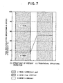
- a C-mode non-defective ratio of a dielectric breakdown strength test in oxides under the same electric field strength with an increased passage time of 60 min. or longer for a range between 1,150°C and 1,080°C according to the present invention reached to a value of as high as 80 % or higher as the case (B) shown in FIG. 7 and such a non-defective ratio was greatly higher in contrast with a ratio in the traditional case (C) shown in FIG. 7, in which a C-mode non-defective ratio fell in a range of 40 % to 60 %.
- the inventors of the present invention estimated temperatures in the bulk of a growing crystal in a variety of furnace structures by the numeral analysis method and devised a furnace structure suitable for limiting a gradual cooling process to the temperature range according to the present invention from the results thus obtained by the analysis method.
- a furnace structure is, as shown in FIG. 5 (b), to extend a hollow heat insulating cylinder 5 surrounding a heater 4 upward and place a carbon ring 7 on the upper end of the heat insulating cylinder 5.
- the extension of the heat insulating cylinder 5 and carbon ring 7 are not present in a traditional furnace structure ( FIG. 5 (a) ).
- the heat insulating cylinder 5 has an annular gap 8 for thermal separation in the mid portion between the upper part and lower part to successfully limit a rapid cooling process to a higher temperature range only.
- the annular separation gap 8 functions so as to increase a radiation loss from the growing crystal surface passing the vicinity of the gap 8.
- a vertical position of the gap 8 is important by the reason above mentioned and it is necessary to locate the gap 8 at a position at least higher than the height of the melt surface.
- a variety of analyses were done in regard to a width of the opening of the annular gap 8 and the results were such that the maximal width should be 10 cm because the effect of a gradual cooling in a temperature range of 1,150°C to 1,080°C was lost if a width of the gap was very large.
- FIGS. 6 (a) and 6 (b) A temperature profile along the length of a growing crystal in such a furnace structure was measured and the results were, as shown in FIGS. 6 (a) and 6 (b), that a passage time in a higher temperature range was made shorter and a passage time in a temperature range between 1,150°C and 1,080°C was made longer compared with that in a traditional furnace structure.
- FIG. 6 (b) a time required for growing crystal to pass a temperature difference of 50°C is plotted on an ordinate as a function of a temperature of the growing crystal on an abscissa.
- the present invention it becomes possible to decrease an absolute density of crystal defect nuclei, since a passage time for a growing crystal in a temperature range between 1,150°C and 1,080°C gets about 1.6 times as long as that in a traditional furnace structure and thereby a point defect is annihilated.
- a temperature gradient in a higher temperature range in the vicinity of the melting point which gradient does not affect the magnitude of a point defect density, can be made steep, a silicon crystal with a low defect density can be grown at a growth rate by about 10 % higher than that in a traditional furnace structure.
Abstract

Description
- The present invention relates to a method of producing a silicon single crystal of an improved dielectric breakdown strength in oxides with a high productivity by means of the Czochralski technique or the pulling technique.
- The recent miniaturization trend of components in a chip following the large scale integration of a semiconductor circuit has demanded a thinner dielectric oxide film of the gate in the MOS-LSI. Even with such a thinner dielectric oxide film, not only a high dielectric breakdown strength but also low current leakage are retained reqirements for a semiconductor device being active, or in other words a high reliability of the oxide film is in a great demand.
- It is known that the dielectric breakdown strength in oxide on a silicon wafer produced from a silicon single crystal grown by means of the Czochralski technique is generally much lower than those on a silicon wafer from the floating zone melting technique or on an epitaxial wafer that is produced by depositing a silicon single crystal thin film on a silicon single crystal wafer grown by means of the Czochralski technique ( see Mitsumasa KOYANAGI: "Submicron Device II-3 Reliability of the Gate Oxide Film" published by Maruzen K. K. Tokyo, page 70 ).
- A major cause of degrading the dielectric breakdown strength in oxide on a silicon wafer from the Czochralski technique has been established to be grown-in crystal defects during the growth. It is also well known that a dieletric breakdown strength in oxide on a silicon single crystal grown by means of the Czochralski technique can be greatly improved by lowering a crystal growth rate to an extremely low value, for example, of 0.4 mm/min. or lower ( see a publication of Unexamined Japanese Patent Application No. Hei 2-267195 ).
- However, when a crystal growth rate is simply lowered from a traditional value of 1 mm/min. or more to a newly proposed value of 0.4 mm/min. or lower in order to improve the dielectric breakdown strength in oxides, productivity of single crystals becomes decreased by half or by more than half compared with that when a traditional growth rate is applied. With such a low growth rate, tremendous increase in the production cost of a single crystal is resulted, though the improvement of dielectric breakdown strength in oxides is attained.
- In light of the above problems which the conventional technology had, the present invention was made to solve them.
- It is an object of the present invention to provide a method of producing a silicon single crystal of an improved dielectric breakdown strength in oxides with a high productivity grown by means of the Czochralski thechnique.
- The present invention was completed through investigations into and studies on relations between the history of thermal conditions under which a single crystal has been growing and grown-in defects in a Czochralski technique. The present invention is directed to a method of producing a silicon single crystal by means of the Czochralski technique comprising the steps of: adjusting a first period required for a growing silicon single crystal to pass a first temperature range from the melting point of silicon ( about 1,420°C ) to 1,200°C in a puller so as to be 190 min. or less; and adjusting a second period for the growing crystal to pass a second temperature range from 1,150°C to 1,080°C in the puller so as to be 60 min. or more, preferably 70 min. or more, and further directed to a silicon single crystal produced by the same method.
- Explanations on the terminology used in the following description will be given below and followed by details of the present invention.
- 1) FPD is an abbreviation for Flow Pattern Defect and a wavelet observable on a treated wafer surface is called FPD. The wavelet is appeared on a wafer surface singly or plurally after a process comprising the steps of: obtaining the wafer slicing an as-grown silicon single crystal; removing the strained surface region by a mixed liquid of hydrofluoric acid and nitric acid, and then further etching the wafer surface with another mixed liquid of hydrofluoric acid and water with K2Cr2O7 as solute to develop pits and wavelets on the surface. A silicon wafer with a larger number of FPDs in a unit surface area shows poorer dielectric breakdown strength in oxides thereon ( see a publication of Unexamined Japanese Patent Application No. Hei 4-192345 ).
- 2) LSTD, which is an abbreviation for Laser Scattering Tomography Defect, is a defect which causes scattered radiation which is detected through a polished surface of a silicon wafer when an incident infrared beam is impinged on a cleaved plane of the silicon wafer, the silicon wafer having been in advance of testing etched to remove the strained surface region with a mixed liquid of hydrofluoric acid and nitric acid and then cleaved in preparation for testing. The cause of the scattered radiation is assumed an oxygen deposit in the bulk of the silicon wafer. Reports on the scatterers thus detected have been made in meetings of academic societies or related journals ( see, for example, Shinsuke SADAMITSU et al.,: Jpn. J. Appl. Phys. Vol. 32 ( 1993 ) pp. 3675-3681 ).
- Theses FPD and LSTD are believed to be factors which cause degradation of the dielectirc breakdown strength in oxides, since each density in a bulk or surface has a correlation with a fraction of defectives. From the observation, a conclusion is deduced that it is necessary that FPD and LSTD should be decreased in order to have improved dielectric breakdown strength in oxides on a silicon single crystal grown by means of the Chohralski technique.
- The inventors investigated into a mechanism in which, with a lowered crystal growth rate, densities of FPDs and LSTDs are decreased and at the same time the dielectric breakdown strength in oxides are improved. In this investigation, the inventors employed two types of furnace structure one of which is suitable for gradual cooling and the other for rapid cooling. It was discovered from the results of experiments that when a crystal growth rate was lowered rapidly from a previous higher growth rate, it was before the turning point in growth rate that the densities of FPDs and LSTDs was rapidly decreased. This fact means the decrease in the densities occurred in a already grown portion.
- A changing point of the densities is different in dependence of a different type of furnace structure. In a type of rapid cooling furnace structure, a changing point of the densities is located at a point of a distance of about 14 cm to 11 cm prior to a turning point in growth rate ( in a region between a point A and a point B on a single crystal shown in FIG. 1 (a) ). In a type of gradual cooling furnace structure, a changing point of the densities is located at a point of a distance of about 19 cm to 16 cm prior to the turning point in growth rate ( in a region between a point A' and a point B' on a single crystal shown in FIG. 1 (a) ). The inventors made an additional discovery in further investigation that temperatures corresponding to the changing points of the densities fall in a range of 1,150°C to 1,080°C ( see FIG. 1 (b) ). That is, since the respective temperatures at the points A and A' , each of which is 1,080°C, on the growing crystals at the starting times when growth rates of both cases were rapidly changed was the lowest temperature in a range capable of affecting densities of FPDs and LSTDs, the respective densities FPDs and LSTDs at the points A and A' were not so different from the densities in the top region of the growing crystal. It is because a period of time for the growing crystal to pass a temperature range from 1,150°C to 1,080°C became continuously longer in a portion grown later owing to the decrease in growth rate that densities of FPDs and LSTDs were rapidly lowered respectively between the points A and B and between the points A' and B'. In respective regions between the points B or B' and the changing point in growth rate on the respective growing crystals, densities of FPDs and LSTDs were respectively kept constant, because the growing crystals can pass the temperature range from 1,150°C to 1,080°C in a constant time, the former of which is the highest temperature capable of affecting the densities.
- The above-mentioned experimental results tell that a temperature region from 1,150°C to 1,080°C affects the process of annihilation of the crystal defects during crystal growth and further that a temperature gradient in a region in the vicinity of the melting points, in other words, a temperature gradient in a high temperature range from a temperature of 1,200°C to the melting point, which affects a growth rate, gives no influence on the process of annihilation of the defects.
- If a crystal growth rate is lowered to excess, the whole growing crystal spends a long time to pass any temperature ranges and therefore a time for passing a range of 1,150°C to 1,080°C gets also longer enough to considerably decrease densities of FPDs and LSTDs and thereby improve the dielectric breakdown strength in oxides.
- As a conclusion, if only a period of time for a growing crystal to pass a temperature range of 1,150°C to 1,080°C can be kept longer enough, there is no need for extending periods of time for a growing crystal to pass other temperature ranges, especially to pass a high temperature range from the melting point to 1,200°C, which affects a crystal growth rate, and therefore a higher crystal growth rate can be realized while attaining great decrease in densities of the defects.
- The inventors designed two types of furnace structure by means of the numerical analysis method setting a border line at about 1,200°C, in a first type (A) of which a gradual cooling prevails in a temperature range of 1,200°C or higher and a rapid cooling prevails at a temperature range of 1,200°C or lower, and in the other type (B) of furnace structure of which a rapid cooling prevails at a temperature range of 1,200°C of higher and a gradual cooling prevails in a range of 1,200°C or lower, or more particularly in a range between 1,150°C and 1,080°C. The newly designed furnace structures (A) and (B) were actually used to grow crystals respectively and crystals grown were compared with crystals from a traditional type (C) of furnace structure in which a rapid cooling prevails in both temperature ranges higher and lower than 1,200°C. The results of the comparison are shown in FIGS. 2 (a), 2 (b), 3 (a) and 3 (b) wherein FPD or LSTD on ordinates as functions of passage times are plotted on respective abscissas in ranges between the melting point and 1,200°C in FIGS. 2 (a) and 3 (a) or between 1,150°C and 1,080°C in FIGS. 2 (b) and 3 (b).
- It can be seen from FIGS. 2 (a), 2 (b), 3 (a) and 3 (b) that the FPD and LSTD have no correlation with the passage time between the melting point and 1,200°C and has a good correlation with the passage time between 1,150°C and 1,080°C. That is, in the case of (A) that a gradual cooling is only applied to a temperature region of 1,200°C or higher, neither the FPD nor LSTD decreases and both defect densities increased to higher values than those in a traditional case (C). However, in the case (B) that a gradual cooling was applied in a temperature range between 1,150°C and 1,080°C while the same crystal growth rate as in the traditional case (C) was adopted, it was found that even with a rapid cooling applied in a temperature range of 1,200°C or higher, the FPD and LSTD each decreased to a value by half or more than half lower than those in the traditional case (C).
- Further experiments similar to those above mentioned were conducted in a variety of types of furnace structure. In the experiments, a correlation was investigated between the FPD and a passage time from 1,150°C to 1,080°C and the results were that a very good correlation was seen therebetween as shown in FIG. 4. Especially, in the case of a passage time of 60 min. or longer, it was found that a FPD density decreases to a value of 500 FPDs/cm2 or lower and in the case of a passage time of 70 min. or longer a FPD density further decreases to a value of 400 FPDs/cm2 or lower.
- A C-mode non-defective ratio of a dielectric breakdown strength test in oxides under an electric field strength of 8 MV/cm, which has a correlation with a FPD density, improved with an increased passage time. A C-mode non-defective ratio of a dielectric breakdown strength test in oxides under the same electric field strength with an increased passage time of 60 min. or longer for a range between 1,150°C and 1,080°C according to the present invention reached to a value of as high as 80 % or higher as the case (B) shown in FIG. 7 and such a non-defective ratio was greatly higher in contrast with a ratio in the traditional case (C) shown in FIG. 7, in which a C-mode non-defective ratio fell in a range of 40 % to 60 %.
- It was found from the above results that a gradual cooling in a temperature range between 1,150°C to 1,080°C in the course of growth makes it possible to obtain a silicon single crystal with high dielectric breakdown strength in oxides thereon. An easy way to adjust a passage time to a value of 60 min. or longer may be to choose an extremely low growth rate of 0.4 mm/min. or less. However, in this case, the productivity becomes very low as described above and therefore the object of the present invention cannot be attained. With a traditional furnace structure, it is difficult to gradually cool a growing crystal in this particular temperature range only and therefore when choosing an extremely low growth rate, a temperature gradient in the vicinity of the melting point in the bulk becomes smaller. The difficulty in limiting a gradual cooling to such a specified temperature range makes it indispensable to reduce a growth rate by 10 % or more.
- The inventors of the present invention estimated temperatures in the bulk of a growing crystal in a variety of furnace structures by the numeral analysis method and devised a furnace structure suitable for limiting a gradual cooling process to the temperature range according to the present invention from the results thus obtained by the analysis method. Such a furnace structure is, as shown in FIG. 5 (b), to extend a hollow
heat insulating cylinder 5 surrounding aheater 4 upward and place a carbon ring 7 on the upper end of theheat insulating cylinder 5. The extension of theheat insulating cylinder 5 and carbon ring 7 are not present in a traditional furnace structure ( FIG. 5 (a) ). Theheat insulating cylinder 5 has anannular gap 8 for thermal separation in the mid portion between the upper part and lower part to successfully limit a rapid cooling process to a higher temperature range only. Theannular separation gap 8 functions so as to increase a radiation loss from the growing crystal surface passing the vicinity of thegap 8. A vertical position of thegap 8 is important by the reason above mentioned and it is necessary to locate thegap 8 at a position at least higher than the height of the melt surface. A variety of analyses were done in regard to a width of the opening of theannular gap 8 and the results were such that the maximal width should be 10 cm because the effect of a gradual cooling in a temperature range of 1,150°C to 1,080°C was lost if a width of the gap was very large. - A temperature profile along the length of a growing crystal in such a furnace structure was measured and the results were, as shown in FIGS. 6 (a) and 6 (b), that a passage time in a higher temperature range was made shorter and a passage time in a temperature range between 1,150°C and 1,080°C was made longer compared with that in a traditional furnace structure. In FIG. 6 (b), a time required for growing crystal to pass a temperature difference of 50°C is plotted on an ordinate as a function of a temperature of the growing crystal on an abscissa.
- According to the present invention, it becomes possible to decrease an absolute density of crystal defect nuclei, since a passage time for a growing crystal in a temperature range between 1,150°C and 1,080°C gets about 1.6 times as long as that in a traditional furnace structure and thereby a point defect is annihilated. What's more, according to the present invention, since a temperature gradient in a higher temperature range in the vicinity of the melting point, which gradient does not affect the magnitude of a point defect density, can be made steep, a silicon crystal with a low defect density can be grown at a growth rate by about 10 % higher than that in a traditional furnace structure.
- The novel features which are considered characteristic of the present invention are set forth with particularity in the appended claims. The present invention itself, however, and additional objects and advantages thereof will best be understood from the following description of embodiments thereof when read in connection with the accompanying drawings, in which:
- FIG. 1 (a) is a graph showing a relationship between a position measured in growth length and a FPD density at the position during crystal growth when a growth rate was rapidly changed in the course.
- FIG. 1 (b) is a graph showing a relationship between a position measured in height above the melt surface and a temperature at the position during crystal growth,
- FIG. 2 (a) is a graph showing a relationship between a passage time of a temperature range from the melting point to 1,200°C and a FPD density during crystal growth,
- FIG. 2 (b) is a graph showing a relationship between a passage time of a temperature range from 1,150°C to 1,080°C and a FPD density during crystal growth,
- FIG. 3 (a) is a graph showing a relationship between a passage time of a temperature range from the melting point to 1,200°C and a LSTD density during crystal growth,
- FIG. 3 (b) is a graph showing a relationship between a passage time of a temperature range from 1,150°C to 1,080°C and a LSTD density during crystal growth,
- FIG. 4 (a) is a graph with plots of different marks showing relationships each of which is one between a passage time of a temperature range from the melting point to 1,200°C and a FPD density in each of different furnace structures during crystal growth,
- FIG. 4 (b) is a graph with plots of different marks showing relationships each of which is one between a passage time of a temperature range from 1,150°C to 1,080°C and a FPD density in each of different furnace structures during crystal growth,
- FIG. 5 (a) is a schematic view in a longitudinal section of a furnace for crystal growth having a traditional structure used in the Czochralski technique, in which a rapid cooling prevails along the entire growth length,
- FIG. 5 (b) is a schematic view in a longitudinal section of a furnace for crystal growth having a structure according to the present invention used in the Czochralski technique, in which a gradual cooling is applied in a temperature range from 1,150°C to 1,200°C,
- FIG. 6 (a) is a graph showing relationship of a crystal temperature between the height above the melt surface at which the temperature is measured during crystal growth,
- FIG. 6 (b) is a graph showing relationship of a crystal temperature between a passage time for a temperature difference at the temperature during crystal growth,
- FIG. 7 is a graph comparatively showing characteristics of dielectric breakdown strength in oxide in various mode, in which C shows the characteristics of a crystal grown with a traditional furnace structure and B shows those of another crystal which passed a temperature range of 1,150°C to 1,200°C in 60 min. or longer during crystal growth.
- Below, description will be given about examples according to the present invention and a comparative example in reference to accompanying drawings.
- In the Czochralski technique, a silicon single crystal having a diameter of 6 inches and a growth orientation of < 100 > was grown in a quartz crucible of a diameter of 18 inches and with 50 kg of polycrystal silicon charged as a raw material in a furnace of a traditional structure as shown in FIG. 5 (a) or a furnace of a structure according to the present invention as shown in FIG. 5 (b). As furnace structures in the examples, two types were tried, one of which has a width of the opening of a separation gap of 8 cm, and the other has 4 cm. FPD and LSTD densities measured are shown in Table 1 together with respective average growth rates.
Table 1 Av.growth rate (mm/min.) FPD density ( /cm2) LSTD density (/cm3) Examples Sep. Gap 8 cm1.10 

Sep. gap 4 cm 1.00 

Comp. Example 1.00 

- It can be seen from the results shown in Table 1 that the examples showed great effects of decreasing FPD and LSTD densities in comparison of the data with those of the comparative example, even though growth rates in the examples larger than or equal to that of the comparative example.
Claims (8)
- A method of producing a silicon single crystal by means of the Czochralski technique comprising a step of adjusting a passage time of a growing crystal for a temperature range of 1,150°C to 1,080°C so as to be 60 min. or longer during crystal growth.
- A method of producing a silicon single crystal by means of the Czochralski technique comprising a step of adjusting a passage time of a growing crystal for a temperature range of 1,150°C to 1,080°C so as to be 70 min. or longer during crystal growth.
- A method of producing a silicon single crystal by means of the Czochralski technique comprising steps of adjusting a first passage time of a growing crystal for a first temperature range of the melting point to 1,200°C so as to be 190 min. or shorter and adjusting a second passage time of the growing crystal for a second temperature range of 1,150°C to 1,080°C so as to be 60 min. or longer during crystal growth.
- A method of producing a silicon single crystal by means of the Czochralski technique comprising steps of adjusting a first passage time of a growing crystal for a first temperature range of the melting point to 1,200°C so as to be 190 min. or shorter and a second passage time the growing crystal for a second temperature range of 1,150°C to 1,080°C so as to be 70 min. or longer during crystal growth.
- A silicon single crystal produced by means of a method of producing a silicon single crystal using the Czochralski technique comprising a step of adjusting a passage time of a growing crystal for a temperature range of 1,150°C to 1,080°C so as to be 60 min. or longer during crystal growth.
- A silicon single crystal produced by means of a method of producing a silicon single crystal using the Czochralski technique comprising a step of adjusting a passage time of a growing crystal for a temperature range of 1,150°C to 1,080°C so as to be 70 min. or longer during crystal growth.
- A silicon single crystal produced by means of a method of producing a silicon single crystal using the Czochralski technique comprising steps of adjusting a first passage time of a growing crystal for a first temperature range of the melting point to 1,200°C so as to be 190 min. or shorter and adjusting a second passage time of the growing crystal for a second temperature range of 1,150°C to 1,080°C so as to be 60 min. or longer during crystal growth.
- A silicon single crystal produced by means of a method of producing a silicon single crystal using the Czochralski technique comprising steps of adjusting a first passage time of a growing crystal for a first temperature range of the melting point to 1,200°C so as to be 190 min. or shorter and adjusting a second passage time of the growing crystal for a second temperature range of 1,150°C to 1,080°C so as to be 70 min. or longer during crystal growth.
Applications Claiming Priority (3)
| Application Number | Priority Date | Filing Date | Title |
|---|---|---|---|
| JP14339195 | 1995-06-09 | ||
| JP7143391A JPH08337490A (en) | 1995-06-09 | 1995-06-09 | Silicon single crystal almost free from crystal defect and its production |
| JP143391/95 | 1995-06-09 |
Publications (3)
| Publication Number | Publication Date |
|---|---|
| EP0747513A2 true EP0747513A2 (en) | 1996-12-11 |
| EP0747513A3 EP0747513A3 (en) | 1997-05-28 |
| EP0747513B1 EP0747513B1 (en) | 1999-09-15 |
Family
ID=15337683
Family Applications (1)
| Application Number | Title | Priority Date | Filing Date |
|---|---|---|---|
| EP96303989A Expired - Lifetime EP0747513B1 (en) | 1995-06-09 | 1996-06-03 | Process for proceeding a silicon single crystal with low defect density |
Country Status (5)
| Country | Link |
|---|---|
| US (1) | US5728211A (en) |
| EP (1) | EP0747513B1 (en) |
| JP (1) | JPH08337490A (en) |
| KR (1) | KR100225274B1 (en) |
| DE (1) | DE69604235T2 (en) |
Cited By (13)
| Publication number | Priority date | Publication date | Assignee | Title |
|---|---|---|---|---|
| EP0875607A1 (en) * | 1996-01-19 | 1998-11-04 | Shin-Etsu Handotai Company, Limited | Silicon single crystal with no crystal defect in peripheral part of wafer and process for producing the same |
| EP0909840A1 (en) * | 1997-10-17 | 1999-04-21 | Shin-Etsu Handotai Company Limited | Method for producing a silicon single crystal having few crystal defects, and a silicon single crystal and silicon wafers produced by the method |
| EP0962557A1 (en) * | 1998-06-03 | 1999-12-08 | Shin-Etsu Handotai Company Limited | Silicon single crystal wafer and method for producing silicon single crystal wafer |
| WO2000022196A1 (en) * | 1998-10-14 | 2000-04-20 | Memc Electronic Materials, Inc. | Process for preparing defect free silicon crystals which allows for variability in process conditions |
| US6312516B2 (en) | 1998-10-14 | 2001-11-06 | Memc Electronic Materials, Inc. | Process for preparing defect free silicon crystals which allows for variability in process conditions |
| US6328795B2 (en) | 1998-06-26 | 2001-12-11 | Memc Electronic Materials, Inc. | Process for growth of defect free silicon crystals of arbitrarily large diameters |
| US6409826B2 (en) | 1997-04-09 | 2002-06-25 | Memc Electronic Materials, Inc. | Low defect density, self-interstitial dominated silicon |
| US6416836B1 (en) | 1998-10-14 | 2002-07-09 | Memc Electronic Materials, Inc. | Thermally annealed, low defect density single crystal silicon |
| US6565649B2 (en) | 1998-10-14 | 2003-05-20 | Memc Electronic Materials, Inc. | Epitaxial wafer substantially free of grown-in defects |
| US6835245B2 (en) * | 2000-06-22 | 2004-12-28 | Sumitomo Mitsubishi Silicon Corporation | Method of manufacturing epitaxial wafer and method of producing single crystal as material therefor |
| US6858307B2 (en) | 2000-11-03 | 2005-02-22 | Memc Electronic Materials, Inc. | Method for the production of low defect density silicon |
| US7105050B2 (en) | 2000-11-03 | 2006-09-12 | Memc Electronic Materials, Inc. | Method for the production of low defect density silicon |
| US8216362B2 (en) | 2006-05-19 | 2012-07-10 | Memc Electronic Materials, Inc. | Controlling agglomerated point defect and oxygen cluster formation induced by the lateral surface of a silicon single crystal during CZ growth |
Families Citing this family (15)
| Publication number | Priority date | Publication date | Assignee | Title |
|---|---|---|---|---|
| JPH10152395A (en) * | 1996-11-21 | 1998-06-09 | Komatsu Electron Metals Co Ltd | Production of silicon single crystal |
| US6379642B1 (en) * | 1997-04-09 | 2002-04-30 | Memc Electronic Materials, Inc. | Vacancy dominated, defect-free silicon |
| US6190631B1 (en) * | 1997-04-09 | 2001-02-20 | Memc Electronic Materials, Inc. | Low defect density, ideal oxygen precipitating silicon |
| WO1999010570A1 (en) * | 1997-08-26 | 1999-03-04 | Sumitomo Metal Industries, Ltd. | High-quality silicon single crystal and method of producing the same |
| WO2000013211A2 (en) | 1998-09-02 | 2000-03-09 | Memc Electronic Materials, Inc. | Silicon on insulator structure from low defect density single crystal silicon |
| JP2000154070A (en) * | 1998-11-16 | 2000-06-06 | Suminoe Textile Co Ltd | Ceramic three dimensional structure and its production |
| JP4293395B2 (en) | 1999-04-28 | 2009-07-08 | Sumco Techxiv株式会社 | CZ method single crystal ingot manufacturing apparatus and method |
| US6635587B1 (en) | 1999-09-23 | 2003-10-21 | Memc Electronic Materials, Inc. | Method for producing czochralski silicon free of agglomerated self-interstitial defects |
| DE60010496T2 (en) * | 1999-09-23 | 2005-04-07 | Memc Electronic Materials, Inc. | Czochralski process for producing silicon monocrystals by controlling the cooling rate |
| US6391662B1 (en) | 1999-09-23 | 2002-05-21 | Memc Electronic Materials, Inc. | Process for detecting agglomerated intrinsic point defects by metal decoration |
| JP4718668B2 (en) * | 2000-06-26 | 2011-07-06 | 株式会社Sumco | Epitaxial wafer manufacturing method |
| KR100801672B1 (en) | 2000-06-30 | 2008-02-11 | 신에쯔 한도타이 가부시키가이샤 | Silicon single crystal wafer and method for manufacturing the same |
| DE60213759T2 (en) * | 2001-01-26 | 2006-11-30 | Memc Electronic Materials, Inc. | SILICON WITH LOW DEFECT DENSITY AND EMPTY-DOMINANTED CORE THAT IS ESSENTIALLY FREE FROM OXIDATION-INDUCED STACKING ERRORS |
| TW200428637A (en) * | 2003-01-23 | 2004-12-16 | Shinetsu Handotai Kk | SOI wafer and production method thereof |
| WO2015125425A1 (en) * | 2014-02-24 | 2015-08-27 | 信越半導体株式会社 | Method for manufacturing silicon single crystal and silicon single crystal |
Citations (5)
| Publication number | Priority date | Publication date | Assignee | Title |
|---|---|---|---|---|
| EP0355833A2 (en) * | 1988-08-25 | 1990-02-28 | Shin-Etsu Handotai Company Limited | Method of producing compound semiconductor single crystal |
| JPH02267195A (en) * | 1989-04-05 | 1990-10-31 | Nippon Steel Corp | Silicon single crystal excellent in withstand voltage characteristic of oxide film and production thereof |
| EP0504837A2 (en) * | 1991-03-20 | 1992-09-23 | Shin-Etsu Handotai Company Limited | Method and apparatus for producing silicon single crystal |
| US5152867A (en) * | 1990-03-12 | 1992-10-06 | Osaka Titanium Co., Ltd. | Apparatus and method for producing silicon single crystal |
| JPH0761889A (en) * | 1993-08-26 | 1995-03-07 | Komatsu Electron Metals Co Ltd | Semiconductor single crystal pull device and method fir pulling semiconductor single crystal |
Family Cites Families (5)
| Publication number | Priority date | Publication date | Assignee | Title |
|---|---|---|---|---|
| DD258427A1 (en) * | 1987-03-16 | 1988-07-20 | Freiberg Spurenmetalle Veb | METHOD AND ARRANGEMENT FOR MONITORING AND REGULATING CRYSTAL CROPS PROCESSES |
| JPH0777995B2 (en) * | 1989-11-16 | 1995-08-23 | 信越半導体株式会社 | Single crystal resistivity control method |
| JPH06103714B2 (en) * | 1990-11-22 | 1994-12-14 | 信越半導体株式会社 | Method for inspecting electrical characteristics of silicon single crystal |
| DE4301072B4 (en) * | 1993-01-16 | 2006-08-24 | Crystal Growing Systems Gmbh | Process for pulling single crystals from a melt |
| JP3285111B2 (en) * | 1994-12-05 | 2002-05-27 | 信越半導体株式会社 | Method for producing silicon single crystal with few crystal defects |
-
1995
- 1995-06-09 JP JP7143391A patent/JPH08337490A/en active Pending
-
1996
- 1996-06-03 EP EP96303989A patent/EP0747513B1/en not_active Expired - Lifetime
- 1996-06-03 US US08/660,198 patent/US5728211A/en not_active Expired - Fee Related
- 1996-06-03 DE DE69604235T patent/DE69604235T2/en not_active Expired - Fee Related
- 1996-06-05 KR KR1019960019997A patent/KR100225274B1/en not_active IP Right Cessation
Patent Citations (5)
| Publication number | Priority date | Publication date | Assignee | Title |
|---|---|---|---|---|
| EP0355833A2 (en) * | 1988-08-25 | 1990-02-28 | Shin-Etsu Handotai Company Limited | Method of producing compound semiconductor single crystal |
| JPH02267195A (en) * | 1989-04-05 | 1990-10-31 | Nippon Steel Corp | Silicon single crystal excellent in withstand voltage characteristic of oxide film and production thereof |
| US5152867A (en) * | 1990-03-12 | 1992-10-06 | Osaka Titanium Co., Ltd. | Apparatus and method for producing silicon single crystal |
| EP0504837A2 (en) * | 1991-03-20 | 1992-09-23 | Shin-Etsu Handotai Company Limited | Method and apparatus for producing silicon single crystal |
| JPH0761889A (en) * | 1993-08-26 | 1995-03-07 | Komatsu Electron Metals Co Ltd | Semiconductor single crystal pull device and method fir pulling semiconductor single crystal |
Non-Patent Citations (2)
| Title |
|---|
| PATENT ABSTRACTS OF JAPAN vol. 015, no. 027 (C-0797), 22 January 1991 & JP 02 267195 A (NIPPON STEEL CORP;OTHERS: 01), 31 October 1990, * |
| PATENT ABSTRACTS OF JAPAN vol. 095, no. 006, 31 July 1995 & JP 07 061889 A (KOMATSU ELECTRON METALS CO LTD), 7 March 1995, * |
Cited By (26)
| Publication number | Priority date | Publication date | Assignee | Title |
|---|---|---|---|---|
| US6120749A (en) * | 1996-01-19 | 2000-09-19 | Shin-Etsu Handotai Co., Ltd | Silicon single crystal with no crystal defect in peripheral part of wafer and process for producing the same |
| EP0875607A4 (en) * | 1996-01-19 | 1999-04-14 | Shinetsu Handotai Kk | Silicon single crystal with no crystal defect in peripheral part of wafer and process for producing the same |
| EP0875607A1 (en) * | 1996-01-19 | 1998-11-04 | Shin-Etsu Handotai Company, Limited | Silicon single crystal with no crystal defect in peripheral part of wafer and process for producing the same |
| US6409826B2 (en) | 1997-04-09 | 2002-06-25 | Memc Electronic Materials, Inc. | Low defect density, self-interstitial dominated silicon |
| US6632278B2 (en) | 1997-04-09 | 2003-10-14 | Memc Electronic Materials, Inc. | Low defect density epitaxial wafer and a process for the preparation thereof |
| US6120598A (en) * | 1997-10-17 | 2000-09-19 | Shin-Etsu Handotai Co., Ltd. | Method for producing a silicon single crystal having few crystal defects, and a silicon single crystal and silicon wafers produced by the method |
| US6027562A (en) * | 1997-10-17 | 2000-02-22 | Shin-Etsu Handotai Co., Ltd | Method for producing a silicon single crystal having few crystal defects, and a silicon single crystal and silicon wafers produced by the method |
| EP0909840A1 (en) * | 1997-10-17 | 1999-04-21 | Shin-Etsu Handotai Company Limited | Method for producing a silicon single crystal having few crystal defects, and a silicon single crystal and silicon wafers produced by the method |
| US6299982B1 (en) | 1998-06-03 | 2001-10-09 | Shin-Etsu Handotai Co., Ltd. | Silicon single crystal wafer and method for producing silicon single crystal wafer |
| EP0962557A1 (en) * | 1998-06-03 | 1999-12-08 | Shin-Etsu Handotai Company Limited | Silicon single crystal wafer and method for producing silicon single crystal wafer |
| US6562123B2 (en) | 1998-06-26 | 2003-05-13 | Memc Electronic Materials, Inc. | Process for growing defect-free silicon wherein the grown silicon is cooled in a separate chamber |
| US6913647B2 (en) | 1998-06-26 | 2005-07-05 | Memc Electronic Materials, Inc. | Process for cooling a silicon ingot having a vacancy dominated region to produce defect free silicon |
| US6328795B2 (en) | 1998-06-26 | 2001-12-11 | Memc Electronic Materials, Inc. | Process for growth of defect free silicon crystals of arbitrarily large diameters |
| US6416836B1 (en) | 1998-10-14 | 2002-07-09 | Memc Electronic Materials, Inc. | Thermally annealed, low defect density single crystal silicon |
| US6500255B2 (en) | 1998-10-14 | 2002-12-31 | Memc Electronic Materials, Inc. | Process for growing silicon crystals which allows for variability in the process conditions while suppressing the formation of agglomerated intrinsic point defects |
| US6565649B2 (en) | 1998-10-14 | 2003-05-20 | Memc Electronic Materials, Inc. | Epitaxial wafer substantially free of grown-in defects |
| US6312516B2 (en) | 1998-10-14 | 2001-11-06 | Memc Electronic Materials, Inc. | Process for preparing defect free silicon crystals which allows for variability in process conditions |
| US6652646B2 (en) | 1998-10-14 | 2003-11-25 | Memc Electronic Materials, Inc. | Process for growing a silicon crystal segment substantially free from agglomerated intrinsic point defects which allows for variability in the process conditions |
| US6743289B2 (en) | 1998-10-14 | 2004-06-01 | Memc Electronic Materials, Inc. | Thermal annealing process for producing low defect density single crystal silicon |
| WO2000022196A1 (en) * | 1998-10-14 | 2000-04-20 | Memc Electronic Materials, Inc. | Process for preparing defect free silicon crystals which allows for variability in process conditions |
| US7097718B2 (en) | 1998-10-14 | 2006-08-29 | Memc Electronic Materials, Inc. | Single crystal silicon wafer having an epitaxial layer substantially free from grown-in defects |
| US6835245B2 (en) * | 2000-06-22 | 2004-12-28 | Sumitomo Mitsubishi Silicon Corporation | Method of manufacturing epitaxial wafer and method of producing single crystal as material therefor |
| US6858307B2 (en) | 2000-11-03 | 2005-02-22 | Memc Electronic Materials, Inc. | Method for the production of low defect density silicon |
| US7105050B2 (en) | 2000-11-03 | 2006-09-12 | Memc Electronic Materials, Inc. | Method for the production of low defect density silicon |
| US8216362B2 (en) | 2006-05-19 | 2012-07-10 | Memc Electronic Materials, Inc. | Controlling agglomerated point defect and oxygen cluster formation induced by the lateral surface of a silicon single crystal during CZ growth |
| US8673248B2 (en) | 2006-05-19 | 2014-03-18 | Memc Electronic Materials, Inc. | Silicon material with controlled agglomerated point defects and oxygen clusters induced by the lateral surface |
Also Published As
| Publication number | Publication date |
|---|---|
| EP0747513A3 (en) | 1997-05-28 |
| DE69604235T2 (en) | 2000-03-16 |
| KR100225274B1 (en) | 1999-10-15 |
| US5728211A (en) | 1998-03-17 |
| JPH08337490A (en) | 1996-12-24 |
| EP0747513B1 (en) | 1999-09-15 |
| DE69604235D1 (en) | 1999-10-21 |
Similar Documents
| Publication | Publication Date | Title |
|---|---|---|
| US5728211A (en) | Silicon single crystal with low defect density and method of producing same | |
| EP2144280B1 (en) | Silicon wafer and method for manufacturing the same | |
| KR100582240B1 (en) | Silicon single crystal wafer and a method for producing it | |
| EP0962555B1 (en) | Process for producing a single crystal | |
| EP1270769B1 (en) | Method for producing silicon single crystal having no flaw | |
| EP0890662B1 (en) | Method and apparatus for manufacturing a silicon single crystal having few crystal defects, and a silicon single crystal and silicon wafers manufactured by the same | |
| EP1804283B1 (en) | Manufacturing method of annealed wafer | |
| KR100453850B1 (en) | Silicon single crystal with no crystal defect in peripheral part of wafer | |
| DE112013001054B4 (en) | Method of manufacturing a silicon single crystal wafer | |
| DE69908965T2 (en) | HEAT TEMPERATURE SINGLE CRYSTAL SILICON WITH LOW ERROR DENSITY | |
| KR100581046B1 (en) | A method for producing a silicon single crystal wafer and a silicon single crystal wafer | |
| KR100971163B1 (en) | Annealed wafer and annealed wafer manufacturing method | |
| US5137847A (en) | Method of producing GaAs single crystal substrate using three stage annealing and interstage etching | |
| KR20040107504A (en) | Silico single crystal wafer and epitaxial wafer, and method for prodcing silicon single crystal | |
| US7204881B2 (en) | Silicon wafer for epitaxial growth, an epitaxial wafer, and a method for producing it | |
| US6056931A (en) | Silicon wafer for hydrogen heat treatment and method for manufacturing the same | |
| US6709957B2 (en) | Method of producing epitaxial wafers | |
| KR19980070037A (en) | Optimization method of pulling rate of seed crystal during semiconductor ingot growth, semiconductor ingot growth method using the same, semiconductor ingot and semiconductor wafer and semiconductor device grown accordingly | |
| US6544332B1 (en) | Method for manufacturing silicon single crystal, silicon single crystal manufactured by the method, and silicon wafer | |
| KR20020060244A (en) | Method for manufacturing annealed wafer and annealed wafer | |
| JP2503697B2 (en) | Method for producing semi-insulating GaAs single crystal | |
| US6461447B1 (en) | Substrate for epitaxial growth | |
| JP2003321297A (en) | Method for producing silicon single crystal and silicon single crystal wafer | |
| KR20010101046A (en) | Silicon single crystal and production method for silicon single crystal wafer |
Legal Events
| Date | Code | Title | Description |
|---|---|---|---|
| PUAI | Public reference made under article 153(3) epc to a published international application that has entered the european phase |
Free format text: ORIGINAL CODE: 0009012 |
|
| AK | Designated contracting states |
Kind code of ref document: A2 Designated state(s): DE FR GB |
|
| PUAL | Search report despatched |
Free format text: ORIGINAL CODE: 0009013 |
|
| AK | Designated contracting states |
Kind code of ref document: A3 Designated state(s): DE FR GB |
|
| 17P | Request for examination filed |
Effective date: 19970426 |
|
| 17Q | First examination report despatched |
Effective date: 19970630 |
|
| GRAG | Despatch of communication of intention to grant |
Free format text: ORIGINAL CODE: EPIDOS AGRA |
|
| GRAG | Despatch of communication of intention to grant |
Free format text: ORIGINAL CODE: EPIDOS AGRA |
|
| GRAG | Despatch of communication of intention to grant |
Free format text: ORIGINAL CODE: EPIDOS AGRA |
|
| GRAH | Despatch of communication of intention to grant a patent |
Free format text: ORIGINAL CODE: EPIDOS IGRA |
|
| GRAH | Despatch of communication of intention to grant a patent |
Free format text: ORIGINAL CODE: EPIDOS IGRA |
|
| GRAA | (expected) grant |
Free format text: ORIGINAL CODE: 0009210 |
|
| AK | Designated contracting states |
Kind code of ref document: B1 Designated state(s): DE FR GB |
|
| PG25 | Lapsed in a contracting state [announced via postgrant information from national office to epo] |
Ref country code: FR Free format text: LAPSE BECAUSE OF FAILURE TO SUBMIT A TRANSLATION OF THE DESCRIPTION OR TO PAY THE FEE WITHIN THE PRESCRIBED TIME-LIMIT Effective date: 19990915 |
|
| REF | Corresponds to: |
Ref document number: 69604235 Country of ref document: DE Date of ref document: 19991021 |
|
| EN | Fr: translation not filed | ||
| PG25 | Lapsed in a contracting state [announced via postgrant information from national office to epo] |
Ref country code: GB Free format text: LAPSE BECAUSE OF NON-PAYMENT OF DUE FEES Effective date: 20000603 |
|
| PLBE | No opposition filed within time limit |
Free format text: ORIGINAL CODE: 0009261 |
|
| STAA | Information on the status of an ep patent application or granted ep patent |
Free format text: STATUS: NO OPPOSITION FILED WITHIN TIME LIMIT |
|
| 26N | No opposition filed | ||
| GBPC | Gb: european patent ceased through non-payment of renewal fee |
Effective date: 20000603 |
|
| PGFP | Annual fee paid to national office [announced via postgrant information from national office to epo] |
Ref country code: DE Payment date: 20020612 Year of fee payment: 7 |
|
| PG25 | Lapsed in a contracting state [announced via postgrant information from national office to epo] |
Ref country code: DE Free format text: LAPSE BECAUSE OF NON-PAYMENT OF DUE FEES Effective date: 20040101 |