EP0762818A2 - Device for manufacturing a connection to a circuit board - Google Patents
Device for manufacturing a connection to a circuit board Download PDFInfo
- Publication number
- EP0762818A2 EP0762818A2 EP96114209A EP96114209A EP0762818A2 EP 0762818 A2 EP0762818 A2 EP 0762818A2 EP 96114209 A EP96114209 A EP 96114209A EP 96114209 A EP96114209 A EP 96114209A EP 0762818 A2 EP0762818 A2 EP 0762818A2
- Authority
- EP
- European Patent Office
- Prior art keywords
- circuit board
- counter bearing
- carrier
- pad
- printed circuit
- Prior art date
- Legal status (The legal status is an assumption and is not a legal conclusion. Google has not performed a legal analysis and makes no representation as to the accuracy of the status listed.)
- Withdrawn
Links
Images

Classifications
-
- H—ELECTRICITY
- H05—ELECTRIC TECHNIQUES NOT OTHERWISE PROVIDED FOR
- H05K—PRINTED CIRCUITS; CASINGS OR CONSTRUCTIONAL DETAILS OF ELECTRIC APPARATUS; MANUFACTURE OF ASSEMBLAGES OF ELECTRICAL COMPONENTS
- H05K7/00—Constructional details common to different types of electric apparatus
- H05K7/14—Mounting supporting structure in casing or on frame or rack
- H05K7/1438—Back panels or connecting means therefor; Terminals; Coding means to avoid wrong insertion
- H05K7/1439—Back panel mother boards
-
- H—ELECTRICITY
- H05—ELECTRIC TECHNIQUES NOT OTHERWISE PROVIDED FOR
- H05K—PRINTED CIRCUITS; CASINGS OR CONSTRUCTIONAL DETAILS OF ELECTRIC APPARATUS; MANUFACTURE OF ASSEMBLAGES OF ELECTRICAL COMPONENTS
- H05K7/00—Constructional details common to different types of electric apparatus
- H05K7/14—Mounting supporting structure in casing or on frame or rack
Landscapes
- Engineering & Computer Science (AREA)
- Microelectronics & Electronic Packaging (AREA)
- Coupling Device And Connection With Printed Circuit (AREA)
Abstract
Description
Die Erfindung betrifft eine Vorrichtung zur Herstellung einer elektrischen Verbindung.The invention relates to a device for producing an electrical connection.
An elektrische Verbindungen, insbesondere Steckverbindungen, werden in der Praxis hohe Anforderungen gestellt, denn sie müssen unter verschiedenen Belastungen, wie z.B. Schwingungen, Temperaturunterschiede usw. gewährleisten, daß die durch die Steckverbindung hergestellten Kontakte nicht gelöst werden. Des weiteren sollen diese Verbindungen bedienungsfreundlich hinsichtlich des Herstellens und des Lösens der Verbindung sein.In practice, high demands are placed on electrical connections, in particular plug connections, because they have to be subjected to various loads, e.g. Vibrations, temperature differences, etc. ensure that the contacts made by the connector are not released. Furthermore, these connections are intended to be user-friendly with regard to the production and release of the connection.
Damit eine Steckverbindung diese Anforderungen erfüllen kann, bedarf sie einer Verriegelungsvorrichtung zum Verschieben und Lösen der Teile der Steckverbindung. Durch eine solche Vorrichtung wird sichergestellt, daß alle Kontakte geschlossen werden und zum anderen, daß diese Kontakte sich nicht von selbst während des Betriebes lösen.So that a plug connection can meet these requirements, it requires a locking device for moving and releasing the parts of the plug connection. Such a device ensures that all contacts are closed and, on the other hand, that these contacts do not come loose during operation.
In der europäischen Patentanmeldung EP 03 69 025 ist eine Vorrichtung beschrieben, mit der Karten mit der Platine verbunden und wieder gelöst werden können. Die Vorrichtung besteht aus einem elastischen Rastteil, das mit der Karte verbunden ist, wobei das Rastteil ein bewegliches Endteil aufweist und einen Bedienungshebel, der drehbar an der Karte gelagert ist. Bedienungshebel und Rastteil sind so zueinander angeordnet, daß beim Drehen des Bedienungshebels das Rastteil aufgrund der gekrümmten Oberfläche des Bedienungshebels eine translatorische Bewegung ausführt, wodurch eine Verbindung zwischen Karte und Platine hergestellt wird. Ist eine wirksame Verbindung hergestellt, fällt das bewegliche Endteil in eine am Bedienungshebel vorgesehene Nut ein und verharrt in dieser Position, wodurch die Karte in dieser Position fixiert wird.In European patent application EP 03 69 025 a device is described with which cards can be connected to the circuit board and released again. The device consists of an elastic locking part which is connected to the card, the locking part having a movable end part and an operating lever which is rotatably mounted on the card. The operating lever and the locking part are arranged with respect to one another such that when the operating lever is rotated, the locking part performs a translatory movement due to the curved surface of the operating lever, as a result of which a connection is established between the card and the circuit board. Once an effective connection has been established, the movable end part falls into a groove provided on the operating lever and remains in this position, as a result of which the card is fixed in this position.
Ein Nachteil dieser Vorrichtung liegt insbesondere darin, daß der durch die Einschubkraft ausgeübte Druck dauernd auf der Platine lastet, so daß die Platine während der Verbindung mit der Karte unter starker Spannung steht. Außerdem läßt es sich nicht ausschließen, daß die Einschubkraft aufgrund der vielen Kontakte, die durch die Steckverbindung hergestellt werden müssen, so groß ist, daß sich die Platine durchbiegt. Eine dauerhafte Durchbiegung der Platine führt aber zu Rissen auf der Platine, so daß die aufgedruckten Leitungen zerstört werden. Ein weiterer Nachteil dieser Vorrichtung ergibt sich daraus, daß aufgrund der vorgenannten Probleme die Anzahl der Kontakte, die durch eine Steckverbidnung hergestellt werden können, begrenzt ist, d.h. daß große Karten mit sehr vielen Kontakten mit dieser Vorrichtung nicht verriegelt werden können. Die Funktionen müssen daher auf mehreren Karten verteilt werden, was zu größeren Gehäusen führt.A disadvantage of this device is, in particular, that the pressure exerted by the pushing-in force constantly rests on the circuit board, so that the circuit board is under high tension during connection to the card. In addition, it cannot be ruled out that the insertion force is so great due to the many contacts that have to be made by the plug connection that the circuit board bends. A permanent bending of the board leads to cracks on the board, so that the printed lines are destroyed. Another disadvantage of this device results from the fact that, due to the aforementioned problems, the number of contacts that can be made by a plug connection is limited, i.e. that large cards with a large number of contacts cannot be locked with this device. The functions must therefore be distributed over several cards, which leads to larger housings.
Eine Vorrichtung der eingangs genannten Art zum Verriegeln und Lösen einer Verbindung für elektrische Steckkontakte ist in dem IBM Technical Disclosure Bulletin, Vol. 31, No. 11, April 1989, S. 76-80, beschrieben. Diese Vorrichtung besteht aus Rasthebeln, die an der oberen und unteren Ecke der Karte oder des Schutzgehäuses angeordnet sind, und aus Sperren, die am Gehäuse befestigt sind. Jedem Rasthebel ist eine Sperre funktional derart zugeordnet, daß der Rasthebel erst dann in Eingriff mit der Sperre kommen kann, wenn eine wirksame Verbindung zwischen Karte und Platine hergestellt worden ist. Ein wesentlicher Nachteil dieser Vorrichtung besteht darin, daß der Druck, der zum Verbinden der Karte mit der Platine erforderlich ist, während des gesamten Betriebes auf den Teilen der Steckverbindung lastet. Im übrigen weist diese Vorrichtung die gleichen Nachteile auf, die bei der europäischen Anmeldung EP 03 69 025 aufgeführt worden sind.A device of the type mentioned above for locking and releasing a connection for electrical plug contacts is in the IBM Technical Disclosure Bulletin, Vol. 31, No. 11, April 1989, pp. 76-80. This device consists of locking levers, which are arranged at the upper and lower corner of the card or the protective housing, and locks, which are attached to the housing. A lock is functionally assigned to each locking lever such that the locking lever can only come into engagement with the lock when an effective connection between the card and the circuit board has been established. A major disadvantage of this device is that the pressure required to connect the card to the board is on the parts of the connector during operation. Otherwise, this device has the same disadvantages that were listed in European application EP 03 69 025.
Aus der US 29 93 187 ist eine Vorrichtung bekannt, bei der Rasthebel an am Gehäuse angebrachten, federnden Bügeln angreifen. Durch diese Anordnung können Kräfte quer zur Einschiebevorrichtung auf die Leiterplatte einwirken.From US 29 93 187 a device is known in which engage latching levers on resilient brackets attached to the housing. With this arrangement, forces can act on the circuit board transversely to the insertion device.
Aus der DE 4042060 C1 ist eine Vorrichtung zum Verbindung und Lösen einer elektrischen Steckverbindung bekannt. Die Vorrichtung besteht aus Rasthebeln, die drehbar am unteren und oberen Eckbereich eines Schutzgehäuses bzw. einer Karte angeordnet sind, und flexibel ausgestalteten Teilen, insbesondere Federn, die entweder an einem unflexiblen Sperrteil oder direkt am Gehäuse befestigt sind. An den flexiblen Teilen befindet sich ein Mitnehmerteil.DE 4042060 C1 discloses a device for connecting and disconnecting an electrical plug connection. The device consists of locking levers which are rotatably arranged on the lower and upper corner area of a protective housing or a card, and flexibly designed parts, in particular springs, which are either attached to an inflexible locking part or directly to the housing. There is a driver part on the flexible parts.
Den vorbekannten Vorrichtungen ist der Nachteil gemeinsam, daß damit nur eine relativ begrenzte Anzahl von Verbindungen herstellbar ist. Insbesondere bei Steckverbindungen tritt nämlich das Problem auf, daß bei einer zunehmenden Anzahl der Kontaktstifte die aufzubringende Einschubkraft wächst. Die Einschubkraft darf jedoch ein zulässiges Höchstmaß nicht überschreiten, um eine Beschädigung der Leiterplatten zu vermeiden und auch, um eine aufwändige mechanische Konstruktion zur Aufbringung der erforderlichen Einschubkraft einzusparen. Beispielsweise ist die maximale Anzahl von Verbindungen, die mit der aus der DE 40 42 060 bekannten Vorrichtung herstellbar sind, 600 Verbindungen für eine Leiterplatte.The known devices have the disadvantage in common that only a relatively limited number of connections can be made with them. The problem arises in particular in the case of plug-in connections that the insertion force to be applied increases with an increasing number of contact pins. However, the push-in force must not exceed a permissible maximum in order to avoid damage to the printed circuit boards and also in order to save an expensive mechanical construction for applying the necessary push-in force. For example, the maximum number of connections that can be produced with the device known from DE 40 42 060 is 600 connections for a printed circuit board.
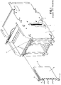
Figur 1 zeigt eine solche aus der DE 40 42 060 bekannte Vorrichtung. Wie Figur 1 zeigt, werden eine oder mehrere Karten 3 parallel nebeneinander in ein Gehäuse 1 eingeführt und innerhalb des Gehäuses 1 mit einer Platine 5 verbunden. Die Karten 3, insbesondere wenn es sich um elektronische Karten handelt, werden üblicherweise in einem Schutzgehäuse 6 zum Schutz gegen elektromagnetische Strahlung gelagert. Dieses Schutzgehäuse 6 ist so gestaltet, daß es eine Öffnung aufweist, aus denen ein Kontaktverbindungsteil 4 herausragt, das mit einem Kontaktverbindungsteil 7 der Platine 5 verbunden wird. Am Schutzgehäuse 6 befindet sich an einer Seite in der oberen und unteren Ecke jeweils ein Rasthebel 9, die schwenkbar am Schutzgehäuse 6 gelagert sind. Soweit aus technischen Gründen auf das Schutzgehäuse 6 zur Abschirmung der Karte 3 verzichtet werden kann, ist die Befestigung des Rasthebels 9 direkt an der Karte 3 möglich.Figure 1 shows such a device known from DE 40 42 060. As FIG. 1 shows, one or more cards 3 are inserted in parallel into a housing 1 and connected to a
An dem Gehäuse 1 befindet sich jeweils im oberen und unteren Bereich Sperren 11, in die die Rasthebel 9 erst dann eingreifen können, wenn eine wirksame Verbindung zwischen dem Kontaktverbindungsteil 7 der Platine 5 und dem Kontaktverbindungsteil 4 der Karte 3 hergestellt worden ist. Die Sperren 11 können einzeln oder gemeinsam an einem Teil befestigt, am Gehäuse 1 angebracht sein.On the housing 1 there are
Das Kontaktverbindungsteil 4 kann beispielsweise ein sogenannter 600-Pin Konnektor sein. Eine Erhöhung der Anzahl der Pins über 600 hinaus würde eine zu große Steckkraft erforderlich machen, die durch Muskelkraft nicht mehr aufbringbar wäre und außerdem die Karte 3 oder deren Gehäuse 6 beschädigen könnte.The contact connection part 4 can be a so-called 600-pin connector, for example. An increase in the number of pins beyond 600 would require an excessive plug-in force which would no longer be able to be applied by muscle strength and which could also damage the card 3 or its
Auf Leiterplatten werden zunehmend hochkomplexe Schaltkreise untergebracht, die eine große Anzahl von Verbindungen zur Kommunikation mit der Umgebung, insbesondere mit anderen Leiterplatten, erfordern.Highly complex circuits are increasingly being accommodated on printed circuit boards, which require a large number of connections for communication with the environment, in particular with other printed circuit boards.
Der Erfindung liegt daher die Aufgabe zugrunde, eine Vorrichtung zur Herstellung einer Verbindung zu schaffen, die die Herstellung einer größeren Anzahl von Verbindungen zwischen einer Leiterkarte und einer Träger-Leiterplatte ermöglicht.The invention is therefore based on the object of providing a device for producing a connection which makes it possible to produce a larger number of connections between a printed circuit board and a carrier printed circuit board.
Das der Erfindung zugrundeliegende Problem wird durch die Merkmale der unabhängigen Ansprüche gelöst.The problem underlying the invention is solved by the features of the independent claims.
Im Gegensatz zu der im Stand der Technik verwendeten "Pin-and-Hole" Technologie, kommen bei der erfindungsgemäßen Vorrichtung "Pad-on-Pad" Konnektoren zum Einsatz. Bei Pad-on-Pad Konnektoren wird der elektrische Kontakt über eine Berührungsfläche hergestellt, während bei der herkömmlichen Pin-and-Hole Technologie das Einführen eines Kontaktstiftes in einen entsprechenden Stecker erforderlich ist. Pad-on-Pad Konnektoren als solche sind aus dem Stand der Technik für das sogenannte Module Packaging bekannt sowie für die Verbindung von Kabeln (IBM TDB Vol. 37, Nr. 11, November 1994, Seiten 581-584, IBM Research Disclosure, Nr. 346, Februar 1993, J.L. Rice and F. H. Smith, TDB Nr. 6, November 1992, Seiten 259-260 and TDB März 1985, Seiten 5962-5965 sowie TDB Nr. 6, November 1992, Seiten 259-260).In contrast to the "pin-and-hole" technology used in the prior art, "pad-on-pad" connectors are used in the device according to the invention. With pad-on-pad connectors, the electrical contact is made via a contact surface, whereas with conventional pin-and-hole technology, it is necessary to insert a contact pin into an appropriate connector. Pad-on-pad connectors as such are known from the prior art for so-called module packaging and for connecting cables (IBM TDB Vol. 37, No. 11, November 1994, pages 581-584, IBM Research Disclosure, No. 346, February 1993, JL Rice and FH Smith, TDB No. 6, November 1992, pages 259-260 and TDB March 1985, pages 5962-5965 and TDB No. 6, November 1992, pages 259-260).
Durch den Einsatz von Pad-on-Pad Konnektoren wird die zur Herstelung einer Verbindung zwischen einer Leiterkarte und einer Träger-Leiterplatte erforderliche Einschubkraft minimiert. Das ist vor allem dadurch bedingt, daß die Reibung der Kontaktstifte beim Einstecken in den Gegenstecker entfällt. Die Anzahl der zwischen einer Leiterkarte und einer Träger-Leiterplatte herstellbaren Verbindungen ist deshalb nicht - wie im Stand der Technik - aufgrund der Reibungskräfte auf ca. 600 beschränkt, sondern kann auch zum Beispiel 1800 Verbindungen zur Signalübertragung betragen.The use of pad-on-pad connectors minimizes the insertion force required to establish a connection between a circuit card and a carrier circuit board. This is mainly due to the fact that the friction of the contact pins when inserting into the mating connector is eliminated. The number of connections that can be made between a printed circuit board and a carrier printed circuit board is therefore not limited to about 600, as in the prior art, due to the frictional forces, but can also be, for example, 1,800 connections for signal transmission.
Überdies erlauben Pad-on-Pad Konnektoren eine kompaktere Bauform im Vergleich zu Pin-and-Hole Konnektoren. Deshalb können Leiterkarten und Träger-Leiterplatten, die mit einer erfindungsgemäßen Vorrichtung ausgestattet sind, die gleiche Baugröße haben, wie mit Pin-and-Hole Konnektoren ausgestattete Leiterkarten, obwohl die erfindungsgemäßen Leiterkarten z. B. eine doppelte Anzahl von Signalausgängen aufweisen. Die erfindungsgemäßen Leiterplatten können deshalb so konstruiert werden, daß sie kompatibel sind zu dem in der Fig. 1 gezeigten mechanischen Aufbau.In addition, pad-on-pad connectors allow a more compact design compared to pin-and-hole connectors. Therefore, circuit boards and carrier circuit boards that are equipped with a device according to the invention can have the same size as circuit boards equipped with pin-and-hole connectors, although the circuit cards according to the invention, for. B. have a double number of signal outputs. The printed circuit boards according to the invention can therefore be constructed so that they are compatible with the mechanical structure shown in FIG. 1.
Besonders vorteilhaft ist die Verwendung einer kreisbogenförmig gekrümmten Gegenlagerung zur Anpressung der Träger-Leiterplatte an die Leiterplatte. Wenn die Krümmung der Gegenlagerung der Elastizität des Materials der Gegenlagerung und der Anpresskraft entsprechend gewählt ist, verformt sich die Gegenlagerung bei Einleitung einer Anpresskraft gerade so, daß die Gegenlagerung ihrer gesamten Länge nach an der Träger-Leiterplatte anliegt. Dann ist ein besonders sicherer Kontakt der Leiterplatte und der Träger-Leiterplatte über die Pad-on-Pad Konnektoren sichergestellt.It is particularly advantageous to use a counter bearing which is curved in the form of a circular arc for pressing the carrier circuit board onto the circuit board. If the curvature of the counterbearing is selected according to the elasticity of the material of the counterbearing and the contact pressure, the counter bearing deforms when a contact pressure is introduced so that the counter bearing bears against the carrier circuit board along its entire length. Then a particularly secure contact of the circuit board and the carrier circuit board is ensured via the pad-on-pad connectors.
Die Gegenlagerung kann an der Träger-Leiterplatte mittels elastischer Elemente mit Spiel aufgehängt sein. Das erweist sich bei der Justage der Leiterkarte and der Träger-Leiterkarte während des Einschiebens als vorteilhaft. Die Selbst-Justage wird dadurch unterstützt. Ein weiterer Vorteil der eleastischen Aufhängung ist die Dämpfung von Stößen beim Transport der Träger-Leiterkarte mit der eingebauten Leiterplatte. Die mechanische Belastung der Leiterplatte und damit auch der Träger-Leiterkarte wird dadurch verringert.The counter bearing can be suspended on the carrier circuit board with play using elastic elements. That proves is advantageous when adjusting the circuit board and the carrier circuit board during insertion. This supports self-adjustment. Another advantage of the elastic suspension is the shock absorption when transporting the carrier circuit board with the built-in circuit board. This reduces the mechanical load on the printed circuit board and thus also on the carrier printed circuit board.
Ein Ausführungsbeispiel der Erfindung ist in der Zeichnung dargestellt und wird im folgenden näher beschrieben.An embodiment of the invention is shown in the drawing and will be described in more detail below.
Es zeigen
- Fig. 1
- eine perspektivische Ansicht einer Karte und eines Gehäuses zur Aufnahme mehrerer solcher Karten nach dem Stand der Technik.
- Fig. 2
- eine perspektivische Ansicht einer erfindungsgemäßen Vorrichtung an einer Leiterkarte und einer Träger-Leiterplatte.
- Fig. 3
- die Gegenlagerung in perspektivischer Ansicht,
- Fig. 4
- die Anordnung der Pad-on-Pad Konnektoren auf der Leiterkarte.
- Fig. 1
- a perspective view of a card and a housing for receiving several such cards according to the prior art.
- Fig. 2
- a perspective view of a device according to the invention on a circuit board and a carrier circuit board.
- Fig. 3
- the counter bearing in a perspective view,
- Fig. 4
- the arrangement of the pad-on-pad connectors on the circuit board.
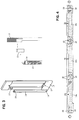
Neben einer aus dem Stand der Technik bekannten Karte 6 (vgl. Fig. 1) ist in der Fig. 2 eine Leiterkarte 12 dargestellt, die einen Pad-on-Pad Konnektor 14 aufweist. Das Gegenstück zu dem Pad-on-Pad Konnektor 14 befindet sich an der Träger-Leiterplatte 13. Die Träger-Leiterplatte 13 entspricht der Platine 5 der Fig. 1, die jedoch lediglich Pin-and-Hole Konnektoren aufweist. Die Karte 6 ist an der Träger-Leiterplatte 13 - wie aus dem Stand der Technik bekannt - mittels eines Pin-and-Hole Konnektors kontaktiert.In addition to a
Dagegen wird die Verbindung zwischen der Leiterkarte 12 und der Trägerleiterkarte 13 erfindungsgemäß durch einen Pad-on-Pad Konnektor 14 hergestellt. In diesem Ausführungsbeispiel besteht der Pad-on-Pad Konnektor 14 aus insgesamt 3 nebeneinander angeordneten Einzelkonnektoren (vgl. Fig. 4).In contrast, the connection between the
Mittels der Schrauben 16 werden der Konnektor 14 und sein an der Träger-Leiterplatte 13 befindliches Gegenstück aneinandergepresst, um eine sichere Kontaktierung zu gewährleisten. Durch die Schrauben 16 wird dabei eine Anpresskraft in die an der Träger-Leiterplatte 13 befindliche Gegenlagerung 15 eingeleitet (vgl. Fig. 3).The
Im übrigen entspricht der mechanische Aufbau dem in der Fig. 1 gezeigten Aufbau. Insbesondere weisen die einzelnen Leiterplatten 12 auch Rasthebel 9 auf.Otherwise, the mechanical structure corresponds to the structure shown in FIG. 1. In particular, the individual printed
Fig. 3 zeigt die Gegenlagerung 15, und einen Ausschnitt aus der Träger-Leiterplatte 13. Die Gegenlagerung 15 wird im zusammengebauten Zustand an der Träger-Leiterplatte 13 mittels elastischer Elemente 17 fixiert. Die elastischen Elemente 17 können beispielsweise aus Kunststoff bestehen. Die Gegenlagerung 15 ist kreisbogenförmig gekrümmt. Der Radius des Kreisbogens ist wesentlich größer als dessen Länge. Der Kreismittelpunkt liegt auf der der Leiterkarte 12 abgewandten Seite.3 shows the counter bearing 15 and a section of the
Die Bohrungen 18 in der Gegenlagerung 15 sind mit einem Innengewinde versehen. Zur Herstellung einer Verbindung zwischen der Leiterkarte 12 und der Träger-Leiterplatte 13 wird zunächst die Leiterplatte 12 in ein Gehäuse eingeschoben, das dem Gehäuse 1 der Fig. 1 entspricht. Durch Betätigung der Rasthebel 9 wird die Leiterkarte 12 bezüglich der Träger-Leiterplatte 13 vorjustiert. Danach werden die Schrauben 16 in die Bohrungen 18 in der Gegenlagerung 15 geschraubt. Dadurch wird eine Anpresskraft in die Gegenlagerung 15 eingeleitet. Gleichzeitig wird der Pad-on-Pad Konnektor 14 bezüglich seines Gegenstücks an der Träger-Leiterplatte 13 während des Festschraubens feinjustiert.The
Bei der in der Zeichnung dargestellten bevorzugten Ausführungsform der Erfindung wird die Vor- und Feinjustage durch die kegelförmigen Elemente 19 bzw. 20 unterstützt (Fig. 4). Die kegelförmigen Elemente 19 und 20 befinden sich an den Einzelkonnektoren 14a, 14b, 14c. Die Elemente 19 und 20 sind zylinderförmig mit einem Kegelstumpfaufsatz, also wie ein angeschrägter Bolzen geformt. Die Elemente 19 sind leicht beweglich schwimmend gehalten, so daß sie ein seitliches Spiel ermöglichen. Die Elemente 20 dagegen sind fest an den Einzelkonnektoren 14a, 14b, 14c fixiert. Den Einzelkonnektoren 14a, 14b, 14c entsprechen Konnektoren auf der Träger-Leiterplatte 13, über die die Signalverbindungen hergestellt werden. Fig.4 zeigt daher quasi einen Abdruck - sog. foot print - der entsprechenden Konnektoren der Träger-Leiterplatte 13.In the preferred embodiment of the invention shown in the drawing, the preliminary and fine adjustment supported by the
Beim Einschieben der Leiterkarte 12 in die Träger-Leiterplatte 13 werden die kegelförmigen Elemente 19 in Aufnahmebohrungen der Träger-Leiterplatte 13 eingeführt. Dies wird durch das seitliche Speil der Elemente 19 erleichtert. Durch die Einführung der kegelförmigen Elemente 19 in ihre entsprechenden Aufnahmebohrungen werden die Konnektoren 14a, 14b, 14c auf ihre entsprechenden Gegenstücke vorjustiert. Die Feinjustage erfolgt dann bei Einführung der Elemente 20 in deren entsprechende Aufnahmebohrungen. Dies geschieht zeitlich nach der Vorjustage, da die Elemente 20 eine geringere Höhenausdehnung als die Elemente 19 aufweisen.When the
Claims (9)
Applications Claiming Priority (2)
| Application Number | Priority Date | Filing Date | Title |
|---|---|---|---|
| DE1995133569 DE19533569C2 (en) | 1995-09-11 | 1995-09-11 | Device for making a connection to a printed circuit board |
| DE19533569 | 1995-09-11 |
Publications (2)
| Publication Number | Publication Date |
|---|---|
| EP0762818A2 true EP0762818A2 (en) | 1997-03-12 |
| EP0762818A3 EP0762818A3 (en) | 1997-05-14 |
Family
ID=7771838
Family Applications (1)
| Application Number | Title | Priority Date | Filing Date |
|---|---|---|---|
| EP96114209A Withdrawn EP0762818A3 (en) | 1995-09-11 | 1996-09-05 | Device for manufacturing a connection to a circuit board |
Country Status (3)
| Country | Link |
|---|---|
| EP (1) | EP0762818A3 (en) |
| JP (1) | JPH09115622A (en) |
| DE (1) | DE19533569C2 (en) |
Families Citing this family (2)
| Publication number | Priority date | Publication date | Assignee | Title |
|---|---|---|---|---|
| DE20117188U1 (en) * | 2001-10-19 | 2002-01-03 | Stocko Contact Gmbh & Co Kg | Adapter for contacting chip cards |
| DE102016118630B3 (en) | 2016-09-30 | 2018-02-22 | Fujitsu Limited | computer system |
Citations (4)
| Publication number | Priority date | Publication date | Assignee | Title |
|---|---|---|---|---|
| DE3917527A1 (en) * | 1989-05-30 | 1990-12-06 | Kloeckner Becorit Gmbh | Control unit for electrohydraulic unit - has sealed connector at rear that provides latched coupling for cables |
| EP0471982A1 (en) * | 1990-08-03 | 1992-02-26 | Siemens Nixdorf Informationssysteme Aktiengesellschaft | Mounting system for electrical function units, especially for data technics |
| EP0526726A2 (en) * | 1991-07-30 | 1993-02-10 | International Business Machines Corporation | Connection device for use in an electrical circuitry system |
| US5395249A (en) * | 1993-06-01 | 1995-03-07 | Westinghouse Electric Corporation | Solder-free backplane connector |
Family Cites Families (6)
| Publication number | Priority date | Publication date | Assignee | Title |
|---|---|---|---|---|
| US2993187A (en) * | 1960-06-29 | 1961-07-18 | South Chester Corp | Module board fastener |
| DE3507482A1 (en) * | 1985-03-02 | 1986-09-04 | Telefonbau Und Normalzeit Gmbh, 6000 Frankfurt | Contact-pressure connector system for multilayer printed-circuit boards |
| KR920008949B1 (en) * | 1988-04-30 | 1992-10-12 | 후지쓰 가부시끼가이샤 | Printed board unit inserting and withdrawing mechanism for electronic circuit devices |
| DE4042060C1 (en) * | 1990-12-28 | 1992-06-25 | International Business Machines Corp., Armonk, N.Y., Us | |
| US5161986A (en) * | 1991-10-15 | 1992-11-10 | Ceridian Corporation | Low inductance circuit apparatus with controlled impedance cross-unders and connector for connecting to backpanels |
| US5254016A (en) * | 1992-06-17 | 1993-10-19 | Compaq Computer Corporation | Interconnect device mounting apparatus for printed circuit boards |
-
1995
- 1995-09-11 DE DE1995133569 patent/DE19533569C2/en not_active Expired - Fee Related
-
1996
- 1996-09-04 JP JP8234548A patent/JPH09115622A/en active Pending
- 1996-09-05 EP EP96114209A patent/EP0762818A3/en not_active Withdrawn
Patent Citations (4)
| Publication number | Priority date | Publication date | Assignee | Title |
|---|---|---|---|---|
| DE3917527A1 (en) * | 1989-05-30 | 1990-12-06 | Kloeckner Becorit Gmbh | Control unit for electrohydraulic unit - has sealed connector at rear that provides latched coupling for cables |
| EP0471982A1 (en) * | 1990-08-03 | 1992-02-26 | Siemens Nixdorf Informationssysteme Aktiengesellschaft | Mounting system for electrical function units, especially for data technics |
| EP0526726A2 (en) * | 1991-07-30 | 1993-02-10 | International Business Machines Corporation | Connection device for use in an electrical circuitry system |
| US5395249A (en) * | 1993-06-01 | 1995-03-07 | Westinghouse Electric Corporation | Solder-free backplane connector |
Non-Patent Citations (1)
| Title |
|---|
| IBM TECHNICAL DISCLOSURE BULLETIN, Bd. 35, Nr. 6, 1.November 1992, Seiten 259-260, XP000314132 "FLEX ADAPTER FOR A PAD-ON-PAD DEMOUNTABLE PACKAGE" * |
Also Published As
| Publication number | Publication date |
|---|---|
| DE19533569C2 (en) | 1997-08-07 |
| EP0762818A3 (en) | 1997-05-14 |
| JPH09115622A (en) | 1997-05-02 |
| DE19533569A1 (en) | 1997-03-13 |
Similar Documents
| Publication | Publication Date | Title |
|---|---|---|
| DE3537400A1 (en) | HOUSING FOR AN EXPANDABLE PERIPHERAL INTERFACE UNIT | |
| DE19654206A1 (en) | Computer system with expandable modules | |
| DE10133662B4 (en) | Connector for connection to a printed circuit board | |
| EP0091080A2 (en) | Strain relief device | |
| DE10116008A1 (en) | Electromechanical device for mounting an electronic assembly on a subrack, in particular for assembling a display instrument recessed in a dashboard | |
| EP1929848B1 (en) | Connection of two semi-conductor plates or flat components by means of a mechanical lock | |
| EP2481126A1 (en) | Multi fork press-in pin | |
| EP0740499A1 (en) | Rail mounting of an equipment | |
| DE4437316A1 (en) | Decentralised input-output module for electronic controls | |
| DE2912740A1 (en) | UNLOCKING AND REMOVAL DEVICE FOR ELECTRICAL CONNECTION AND ELECTRICAL CONNECTION EQUIPPED WITH SUCH DEVICE | |
| EP2240004A1 (en) | Mounting aid for circuit board connector | |
| DE4042060C1 (en) | ||
| DE102016118630B3 (en) | computer system | |
| EP1264369A1 (en) | Plug-in connection | |
| EP2689496B1 (en) | Direct plug element, in particular for vehicle control devices | |
| DE19533569C2 (en) | Device for making a connection to a printed circuit board | |
| EP3358682A1 (en) | Electrical connector and electrical connector system | |
| EP3493333A1 (en) | Electric plug connection for data transmission | |
| DE3806049C2 (en) | ||
| DE102017111878B4 (en) | LED panel with base plate | |
| EP1430567A1 (en) | Device for electrical connection | |
| EP0755176B1 (en) | Device for establishing an electrical and/or optical connection | |
| DE10136361A1 (en) | Connection device for making an electrical contact between an earth wire and an earthed voltage/potential makes a contact between a foil wire and the earthed potential in a motor vehicle. | |
| DE102021214288B3 (en) | Connector strip for an electrical device of a motor vehicle, electrical device and motor vehicle with this electrical device | |
| DE102019215533B3 (en) | Vehicle comprising an antenna device as well as antenna device and fastening device |
Legal Events
| Date | Code | Title | Description |
|---|---|---|---|
| PUAI | Public reference made under article 153(3) epc to a published international application that has entered the european phase |
Free format text: ORIGINAL CODE: 0009012 |
|
| AK | Designated contracting states |
Kind code of ref document: A2 Designated state(s): DE FR GB |
|
| PUAL | Search report despatched |
Free format text: ORIGINAL CODE: 0009013 |
|
| AK | Designated contracting states |
Kind code of ref document: A3 Designated state(s): DE FR GB |
|
| STAA | Information on the status of an ep patent application or granted ep patent |
Free format text: STATUS: THE APPLICATION IS DEEMED TO BE WITHDRAWN |
|
| 18D | Application deemed to be withdrawn |
Effective date: 19971115 |