EP0781055A2 - Improvements in or relating to image display systems - Google Patents
Improvements in or relating to image display systems Download PDFInfo
- Publication number
- EP0781055A2 EP0781055A2 EP96120656A EP96120656A EP0781055A2 EP 0781055 A2 EP0781055 A2 EP 0781055A2 EP 96120656 A EP96120656 A EP 96120656A EP 96120656 A EP96120656 A EP 96120656A EP 0781055 A2 EP0781055 A2 EP 0781055A2
- Authority
- EP
- European Patent Office
- Prior art keywords
- data
- signal
- rgb
- yuv
- control signal
- Prior art date
- Legal status (The legal status is an assumption and is not a legal conclusion. Google has not performed a legal analysis and makes no representation as to the accuracy of the status listed.)
- Withdrawn
Links
Images


Classifications
-
- H—ELECTRICITY
- H04—ELECTRIC COMMUNICATION TECHNIQUE
- H04N—PICTORIAL COMMUNICATION, e.g. TELEVISION
- H04N5/00—Details of television systems
- H04N5/74—Projection arrangements for image reproduction, e.g. using eidophor
-
- H—ELECTRICITY
- H04—ELECTRIC COMMUNICATION TECHNIQUE
- H04N—PICTORIAL COMMUNICATION, e.g. TELEVISION
- H04N9/00—Details of colour television systems
- H04N9/12—Picture reproducers
- H04N9/31—Projection devices for colour picture display, e.g. using electronic spatial light modulators [ESLM]
- H04N9/3179—Video signal processing therefor
- H04N9/3188—Scale or resolution adjustment
-
- H—ELECTRICITY
- H04—ELECTRIC COMMUNICATION TECHNIQUE
- H04N—PICTORIAL COMMUNICATION, e.g. TELEVISION
- H04N9/00—Details of colour television systems
- H04N9/12—Picture reproducers
- H04N9/31—Projection devices for colour picture display, e.g. using electronic spatial light modulators [ESLM]
- H04N9/3102—Projection devices for colour picture display, e.g. using electronic spatial light modulators [ESLM] using two-dimensional electronic spatial light modulators
- H04N9/312—Driving therefor
-
- H—ELECTRICITY
- H04—ELECTRIC COMMUNICATION TECHNIQUE
- H04N—PICTORIAL COMMUNICATION, e.g. TELEVISION
- H04N9/00—Details of colour television systems
- H04N9/12—Picture reproducers
- H04N9/31—Projection devices for colour picture display, e.g. using electronic spatial light modulators [ESLM]
- H04N9/3179—Video signal processing therefor
- H04N9/3182—Colour adjustment, e.g. white balance, shading or gamut
-
- H—ELECTRICITY
- H04—ELECTRIC COMMUNICATION TECHNIQUE
- H04N—PICTORIAL COMMUNICATION, e.g. TELEVISION
- H04N5/00—Details of television systems
- H04N5/74—Projection arrangements for image reproduction, e.g. using eidophor
- H04N5/7416—Projection arrangements for image reproduction, e.g. using eidophor involving the use of a spatial light modulator, e.g. a light valve, controlled by a video signal
- H04N5/7458—Projection arrangements for image reproduction, e.g. using eidophor involving the use of a spatial light modulator, e.g. a light valve, controlled by a video signal the modulator being an array of deformable mirrors, e.g. digital micromirror device [DMD]
- H04N2005/7466—Control circuits therefor
Definitions
- This invention relates to image display systems using spatial light modulators (SLMs), and more particularly to a projection display system designed for high brightness, high contrast applications, such as displays in meeting rooms and lecture halls.
- SLMs spatial light modulators
- SLMs spatial light modulators
- CRTs cathode ray tubes
- DMDs Digital micro-mirror devices
- SLM System for Mobile Communications
- a DMD has an array of micro-mechanical display elements, each having a tiny mirror that is individually addressable by an electronic signal. Depending on the state of its addressing signal, each mirror tilts so that it either does or does not reflect light to the image plane, thereby modulating light incident on the DMD.
- the mirrors may be generally referred to as "display elements", which correspond to the pixels of the image that they generate. Generally, displaying pixel data is accomplished by loading memory cells connected to the display elements. The display elements can maintain their ON “ or OFF " state for controlled display times.
- SLMs operate on similar principles, with an array of display elements that may emit or reflect light simultaneously, such that a complete image is generated by addressing display elements rather than by scanning a screen.
- SLM liquid crystal display
- LCD liquid crystal display
- PWM pulse-width modulation
- pixel intensities are quantized, such that black is 0 time slices, the intensity level represented by the LSB is 1 time slice, and maximum brightness is 2 n -1 time slices.
- Each pixel's quantized intensity determines its on-time during a frame period.
- each pixel with a quantized value of more than 0 is ON " for the number of time slices that correspond to its intensity.
- the viewer's eye integrates the pixel brightness so that the image appears the same as if it were generated with analog levels of light.
- PWM calls for the data to be formatted into "bit-planes", each bit-plane corresponding to a bit weight of the intensity value.
- bit-planes each bit-plane corresponding to a bit weight of the intensity value.
- each frame of data has n bit-planes.
- Each bit-plane has a 0 or 1 value for each display element.
- each bit-plane is separately loaded and the display elements are addressed according to their associated bit-plane values. For example, the bit-plane representing the LSBs of each pixel is displayed for 1 time slice, whereas the bit-plane representing the MSBs is displayed for 2n/2 time slices.
- SLM-based display systems can be all-digital in the sense that, except for A/D conversion of analog inputs at the front end, all, data processing as well as the display process are digital. Display systems are being developed that optimize this all-digital capability.
- One aspect of the invention is a projection display system for displaying images from data obtained from an input signal that may be one of a variety of input signals, each having a different horizontal and vertical input resolution.
- the system uses serial video processors (SVPs) having a given input size and spatial light modulators (SLMs) having a given vertical and horizontal output resolution.
- SVPs serial video processors
- SLMs spatial light modulators
- An analog signal interface provides YUV or RGB data if the input signal is an analog input signal. It detects a signal type of the analog input signal and provides a control signal indicating the signal type, and has an analog-to-digital converter that samples the analog input signal.
- a YUV-data processing unit receives the YUV data and the control signal.
- a digital signal interface provides RGB data if the input signal is a digital input signal. It detects a signal type of the digital input signal and provides a control signal indicating the signal type. It provides the RGB data on three data paths, one data path for each RGB color.
- An RGB-data processing unit receives the RGB data and the control signal. It has three duplicate sets of components, one for each data path from the digital signal interface. Each set of components has FIFO (first-in first-out) memories for creating multiple subpaths within the RGB-data processing unit, down-scaling processors for decreasing the horizontal input resolution to the SVP input size, and an SVP for performing vertical scaling in response to the RGB control signal.
- FIFO first-in first-out
- a picture quality unit receives data from both the YUV-data processing unit and the RGB-data processing unit. It has a matrix multiplier for performing color space conversion if the data is YUV data, a look-up table for performing de-gamma, and FIFO memories for providing data to a frame memory on multiple data paths, thereby providing display-ready RGB data.
- a frame memory has formatting circuitry for formatting the display-ready RGB data into bit-plane format and has memory cells for storing the display-ready RGB data for delivery to the SLMs. Three SLMs, one for each color, generating images based the display-ready RGB data.
- a timing unit is in data communication with each of the above elements of the system. It receives the control signal from either the analog or the digital interface and delivers timing signals in response to the control signal.
- a technical advantage of the invention is that it provides a DMD-based projection display system that is suitable for institutional and professional applications, such as in auditoriums.
- the display is bright even when projected to a very large screen, and the picture quality meets high performance expectations.
- the system is capable of providing displays from a variety of different input signals. It has separate front end data paths for YUV and RGB data. This permits the same YUV components to be used as are used for television display systems.
- the use of two paths also increases available SVP programming capacity for scaling functions. The two paths will permit the system to be easily modified for overlaying images from the two paths. Developments in digital RGB inputs or in other inputs such as HDTV, can be accommodated without affecting the YUV data path.
- the system can also receive data that is already processed.
- serial video processors are used for interlaced scan to progressive scan conversion of YUV data and for scaling both YUV data and RGB data.
- SVPs serial video processors
- the system is designed so that all data processing stays within bandwidth limitations of its internal components. This may require the data to be modified to match the SVP size (by horizontal down-scaling) as well as the SLM resolution (by horizontal or vertical scaling).
- the system is easily adaptable to SLMs having different resolutions.
- SLMs having higher resolutions the system is configured to meet bandwidth requirements for producing images at video rates.
- the larger the SLM resolution the greater the bandwidth required for real time displays.
- the required data throughput for picture quality processing, frame memory, and formatting is achieved with parallel data paths.
- the underlying architecture will support their use without new component designs.
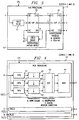
- FIGURE 1 is a block diagram of a projection display system 10, which uses multiple SLMs 18 to generate real-time images from a YUV or an RGB video signal.
- Three SLMs 18 each generate an image of a different color -- red, green, and blue -- with the images combined for a full color display. Only those components significant to main-screen pixel data processing are shown. Other components, such as might be used for processing synchronization and audio signals or secondary screen features, such as closed captioning, are not shown.
- system 10 has DMD-type SLMs 18.
- DMD-type SLMs 18.
- Comprehensive descriptions of DMD-based digital display systems, without features of the present invention, are set out in U.S. Patent No. 5,079,544, entitled “Standard Independent Digitized Video System", in U.S. Patent No. 5,526,051, entitled “Digital Television System”, and in U.S. Patent No. 5,452,024, entitled “DMD Display System, " (each of these patents is assigned to Texas Instruments Incorporated).
- System 10 could also be used with other types of SLMs that have operating characteristics similar to DMDs, notably, the use of RGB bit-plane data.
- the invention is directed to a system 10 that is capable of receiving input signals from a variety of sources.
- the input may be analog, resulting in YUV or RGB data, or digital, resulting in RGB data.
- Each type of data has its own front-end data path, comprised of a signal interface 12 or 14 and a processing unit 13 or 15.
- Both YUV-data processing unit 13 and RGB-data processing unit 15 may be implemented with one or more processors of a type known as serial video processors (SVPs).
- SVP serial video processors
- the SVP is a programmable processor manufactured by Texas Instruments Incorporated.
- the core of the SVP is a one dimensional array of one-bit processing elements, which form a SIMD architecture. Each processing element corresponds to one pixel of a line of video data. In the example of this description, each SVP processes 960 pixels.
- Each SVP has a 40 bit wide data input register and a 24 bit wide data output register. Data input, computation, and data output are concurrent operations. The data rates of the input and output registers are both 33 MHZ.
- the SVPs include memory for storing programming, and depending on the type of input signal, programming appropriate for that signal is selected and executed.
- a feature of the invention is the use of SVPs in YUV processing unit 13 and in RGB processing unit 15 in a manner that permits high resolution images. If the number of active pixels per row of the SLMs 18 exceeds the number of processing elements of the SVP, a down-scaling process is performed before the data enters the SVP. If the required processing exceeds the programming capability of a single SVP, multiple SVPs are connected serially, each programmed to perform different functions.
- each SLM 18 has a specific image resolution, which means that it displays each image using a certain number of display elements per row (horizontal resolution) and a certain number of rows per frame (vertical resolution). This image resolution determines how system 10 must be configured to meet data rate requirements for real time displays. Processing as well as parts configuration is also affected by the SLM resolution. Data may be down-sampled to fit the SVP size and then upscaled to fit the horizonal resolution of SLMs 18. Both types of horizontal scaling (down-scaling and upscaling) may be implemented with parts having the same basic architecture. As the resolution of SLMs 18 increases, system 10 is easily modified by using parallel data paths for picture quality, frame buffering, and formatting tasks.
- analog interface 12 receives an analog video signal, such as an NTSC, PAL, SECAM, or 4.43 NTSC signal.
- an analog video signal such as an NTSC, PAL, SECAM, or 4.43 NTSC signal.
- the following table lists these analog input signals, the number of active lines per frame in the source, and the number of rows displayed by each SLM 18.
- VideoFormat Source Line Resolution DMD Display Resolution NTSC 483 1280x960 PAL 577 1536x1080 SECAM 577 1536x1080 Wide NTSC 483 1706x960
- Analog interface 12 detects the type of input signal, and delivers a control signal to timing unit 19 to indicate the field rate, line rate, and sample rate. It also delivers a control signal to YUV-data processing unit 13 (for YUV data) or to RGB-data processing unit 15 (for RGB data), for selecting the appropriate processing for that type of signal.
- Analog interface 12 separates video, synchronization, and audio signals. It includes components for A/D conversion and Y/UV separation, by which the signal is converted to pixel-data samples and the luminance (“Y”) data is separated from the chrominance (“UV”) data. The signal may be converted to digital data before Y/UV separation, or Y/UV separation could be performed before A/D conversion. Regardless of the order of Y/UV separation and A/D conversion, the output is referred to herein as "YUV data" and is comprised of data representing luminance and chrominance information.
- Analog interface 12 supports different input signals by sampling the analog signal at different pixel rates.
- Color-difference signals such as NTSC signals, may be sampled in accordance with color burst rates, and if there are a different number of samples than the horizontal resolution of SLMs 18, pixels may be added or removed by YUV processing unit 13.
- the luminance component may be sampled by simply dividing the active line period into the appropriate number of sample for the horizontal resolution of SLMs 18, and the chrominance component sampled at the color burst rate and later scaled. This latter method is described in U.S. Patent No. 5,347,321, entitled "Color Separator for Digital Television System". Another sampling method is the subject of European Patent Application 96113923.5.
- the data provided by analog interface 12 has a certain horizontal and vertical data resolution, which may or may not be down-sampled or upscaled, depending on the size of the resolution compared to the input size of any SVP(s) used for processing the data and the image resolution of the SLMs 18.
- YUV-data processing unit 13 prepares the YUV data for display, by performing various data processing tasks.
- Processing unit 13 may include whatever processing memory is useful for such tasks, such as field and line buffers.
- the tasks performed by processing unit 13 include conversion from interlaced to progressive scan format (proscan), scaling, and sharpness control. Interlaced to progressive scan conversion operates on interlaced fields of input data, and generates new data to fill in odd lines of even fields and even lines of odd fields.
- Scaling is the process of changing image resolution, with horizontal scaling changing the number of active pixels per line and vertical scaling changing the number of active lines per frame.
- a digital interface 14 receives the data and detects the type of input signal. It delivers a control signal to timing unit 19 indicating the frame rate and horizontal and vertical resolution, as well as a control signal to RGB-data processing unit 15 to select the appropriate processing. It also performs whatever buffering and timing tasks are needed to prepare the data for processing.
- This data is assumed to be progressively scanned RGB data, such as are the VGA and SVGA formats.
- the RGB data provided by digital interface 14 has a certain horizontal and vertical data resolution, which may or may not be down-sampled or upscaled, depending on the size of the resolution compared to the input size of the SVP(s) used for processing the data and the image resolution of the SLMs 18.
- RGB-data processing unit 15 receives RGB data from either analog interface 12 or digital interface 14. It prepares the RGB data for display, and may include whatever processing memory is useful for such tasks, such as field and line buffers.
- the tasks performed by RGB-data processing unit 15 include scaling, sharpness control, and aperture correction.
- Picture quality unit 16 performs tasks such as color space conversion and de-gamma.
- Colorspace conversion converts Y/C data to RGB data.
- De-gamma undoes gamma correction in signals intended for CRT displays and is required because unlike CRTs, DMDs are linear displays with no inherent gamma characteristics.
- Display memory/format unit 17 receives processed pixel data from picture quality unit 16. It formats the data, on input or on output, into "bit-plane" format, and delivers the bit-planes to SLMs 18 one at a time.
- One SLM 18 receives red bit-planes
- one SLM 18 receives blue bit-planes
- the third SLM 18 receives green bit-planes.
- the bit-plane format permits each display element of SLMs 18 to be turned ON “ or OFF " in response to the value of 1 bit of data at a time.
- this formatting is performed by hardware associated with display memory/format unit 17. However, in other embodiments, the formatting could be performed by processor units 13 and 15 or by dedicated formatting hardware in the data path before or after display memory/format unit 17.
- display memory/format unit 17 has a "double buffer” memory, which means that it has a capacity for at least two display frames.
- the buffer for one display frame can be read out to SLMs 18 while in the buffer another display frame is being written.
- the two buffers are controlled in a "ping-pong" manner so that data is continuously available to SLMs 18.
- the bit-plane data from display memory/format unit 17 is delivered to SLMs 18. Details of a suitable SLM 18 are set out in U.S. Patent No. 4,956,619, entitled “Spatial Light Modulator", which is assigned to Texas Instruments Incorporated. Essentially, each SLM 18 uses the data from display memory/format unit 17 to address each display element of its display element array. The "ON” or “OFF” state of each display element forms an image. The data for different colors (red, green, and blue) is concurrently used to display three images, one on each SLM 18.
- Display optics unit 18a has optical components for illuminating SLMs 18 and for receiving the image from SLMs 18. The images from SLMs 18 are combined by display optics unit 18a to produce a single image.
- Master timing unit 19 provides various system control functions. Timing unit 19 is implemented with a field programmable gate array (FPGA), to handle different frame resolutions and frame rates. As stated above, it receives a control signal from analog interface 12 or from digital interface 14 indicating the type of input signal, so that a corresponding frame rate, line rate, and sample rate (if analog) can be selected. The display frame rate of SLMs 18 is locked to the frame rate of the input signal. For high frame rates, the data resolution (bits per pixel) may be reduced for processing.
- FPGA field programmable gate array
- FIGUREs 2 - 11 illustrate four variations of system 10, each suitable for a system 10 having SLMs 18 of a different resolution, identified in order of increasing resolution, as Resolution Levels 1, 2, 3, and 4.
- SLMs 18 of a different resolution
- YUV-data processing unit 13 and RGB-data processing unit 15 are modified from those of Levels 1 and 2.
- picture quality unit 16 is used in parallel paths.
- the display memory/format unit 17 uses special DMDRAM devices in parallel instead of a VRAM as does a Level 1 system.
- FIGURE 2 is a block diagram of display system 20, configured for SLMs 18 having a resolution of 768 x 576 (Resolution Level 1).
- system 20 has the same basic components as system 10, but the YUV-data processing unit 13, RGB-data processing unit 15, and display memory/format unit 17 are specific to 768 x 576 SLMs 18.
- FIGURE 3 is a block diagram of the YUV-data processing unit 13 of system 20.
- YUV-data processing unit 13 comprises two field delay memories 31 and 32 and two SVPs 33 and 34.
- the SVPs 33 and 34 implement a motion adaptive interlaced to progressive scan conversion process, where the method of generating additional rows of pixel data varies depending on whether there is motion in successive images.
- the field delay memories 31 and 32 and a first SVP 33 are used to obtain a motion value, K ' , for every pixel.
- the second SVP 34 generates pixel data to fill in odd rows of even-row fields and even rows of odd-row fields.
- a method of performing motion adaptive interlaced to progressive scan conversion with an SVP processor is described in U.S. Patent No. 5,526,051, referenced above. Essentially, 4-bit K values, as well as 8-bit pixel values for a current field and a delayed field are used to generate new 10-bit pixels.
- SVP 34 may be further programmed to perform vertical or horizontal scaling if the data does not fit the SLM size.
- a method of performing vertical scaling with an SVP processor is described in U.S. Patent No. 5,526,051, referenced above.
- the data will be sampled at a rate resulting in fewer samples per line than the horizontal resolution of SLMs 18.
- horizontal scaling will be some sort of interpolation process to generate additional pixels. If the data were sampled at a rate that resulted in more pixels per line than the row size of SVP 33, YUV processing unit 13 would have an additional processor (not shown) to reduce the number of pixels per line before the data is input to SVP 33.
- the luminance and chrominance data can be processed at different bit-depths.
- luminance data which is more perceivable to the eye, can be processed as 10-bit data with chrominance data being processed as 7-bit data.
- FIGURE 4 is a block diagram of the RGB-data processing unit 15 of display system 20.
- the data for each color follow a different data path. These three data paths have identical subunits, identified as subunits 15(1), 15(2), and 15(3).
- RGB-data processing unit 15 is used for digital scaling.
- FIFOs 41 are double-row FIFOs, which buffer data to reduce the data rate from digital interface 14.
- the three FIFOs 41 divide the input data rate by a factor of 3.
- a first FIFO 41 receives the data for row 1, then a second FIFO receives the data for row 2, then a third FIFO receives the data for row 3.
- data can be delivered from each FIFO 41 to one of three down-scaling processors 42 along three parallel channels.
- data for one row is being read out of a FIFO 41, data for a new row can be written in.
- Down-scaling processors 42 are used to reduce the data if there are too many pixels per row to fit into SVP 43. For example, if SVP 43 has 960 processing elements and the data has more than 960 samples per line, the data must be downsampled. This downsampling can be as simple as simply removing the data for the extra pixels. Down-scaling processors 42 can be implemented as hardwired logic devices or with programmable processing devices. A technique known as horizontal polyphase resampling may be used for the down-scaling process. As explained below in connection with FIGUREs 7 and 8, this technique may also be used for upscaling in higher resolution systems and permits processors 42 to have the same architecture as other horizontal scaling processors.
- SVP processor 43 performs vertical scaling and aperture correction. It may also perform horizontal interpolation for input data if the number of samples per lines is less than the number of pixels per row of SLMs 18.
- the input register of SVP 43 receives data from down-scaling processors 42 simultaneously, such that data for three different rows is being input in parallel.
- each R,G or B data path is split into three subpaths.
- a multiplexer 44 combines the subpaths back into R,G or B data paths.
- memory/format unit 17 has a formatter and a VRAM memory, which are two separate devices.
- the formatter is a field programmable gate array (FPGA), programmed to format the data into bit-planes. A total of 36 4-Mbit VRAM devices are required.
- FIGURE 5 is a block diagram of a display system 50, configured for SLMs 18 having a resolution of 864 x 576 (Resolution Level 2).
- system 50 is similar to system 20, but has a different memory/format unit 17.
- memory/format unit 17 is comprised of DMDRAMs, which are an application specific device (ASIC).
- DMDRAMs which are an application specific device (ASIC).
- ASIC application specific device
- An example of a suitable DMDRAM is described in Published European Patent document No.0,655,723 assigned to Texas Instruments Incorporated.
- the DMDRAM described therein has a format on output feature but the format could alternatively be performed on input.
- Level 2 SLMs 4 DMDRAM devices are required per SLM 18. Thus, for the three SLMs 18, a total of 12 DMDRAM devices are used in system 50.
- FIGURE 6 is a block diagram of a display system 60, configured for SLMs 18 having a resolution of 1024 x 768 (Resolution Level 3).
- system 60 has the same basic components as system 10, but the YUV-data processing unit 13, RGB-data processing unit 15, and display memory/format unit 17 are specific to 1024 x 768 SLMS 18.
- FIGURE 7 is a block diagram of the YUV-data processing unit 13 of display system 60.
- YUV-data processing unit 13 has the same unit 13 as do systems 20 and 50 for Levels 1 and 2. But for system 60, YUV-data processing unit 13 also accommodates the need to upscale the data for higher resolution SLMs 18.
- FIFOs 71 operate in a manner similar to FIFOs 41 of FIGURE 4, each receiving every third row of data.
- Processors 72 and 73 perform horizontal interpolation and sharpness tasks, respectively. In this system 60, the second SVP would not perform any horizontal scaling, but rather this task is performed by processors 72.
- An example of a sharpness process is described in U.S. Patent No. 5,526,051, referenced above.
- FIGURE 8 is a block diagram of the RGB-data processing unit 15 of display system 60.
- the data for each color has an identical processing unit, identified as units 15(1), 15(2), and 15(3).
- RGB-data processing unit 15 is similar to the RGB-data processing unit 15 of system 20, except that it has a processor 84, which upscales the data if it has been decimated to fit SVP 83. This upscaling is done by an interpolation process and results in the data having the same number of samples per line as display elements per row of SLMs 18.
- Processor 84 may also perform aperture correction, which is especially useful for font-intensive RGB data. For each color, data is output from processing unit 15 in three parallel paths.
- the horizontal scaling processors 72, 82, and 84 may be implemented with hardwired logic or with programmable processors. As stated above, all horizontal scaling may use a horizontal polyphase resampling technique. This permits the horizontal scaling processors 72, 82, and 84 to have the same basic architecture as each other and as the down-scaling processor 42 in FIGURE 4.
- An example of a suitable device for such scaling is the ACUITY device commercially available from Genesis Microchip Incorporated.
- the memory of memory/format unit 17 for system 60 is comprised of the same DMDRAM devices described above for system 20. However, for system 60, 12 DMDRAM devices are required per SLM 18, for a total of 36 DMDRAM devices. The process of transferring data to memory/format unit 17 is described below in connection with FIGURE 11.
- FIGURE 9 is a block diagram of display system 90, configured for SLMs 18 having a resolution of 1280 x 1024 (Resolution Level 4). Other than SLMs 18, system 90 has the same components as system 60. However, because of the "wider" image, the data is more likely to require down scaling to fit the SVP of RGB-data processing unit 15 and subsequent upscaling to match the horizontal resolution of SLMs 18.
- FIGURE 10 is a block diagram of picture quality unit 16.
- Picture quality unit 16 is implemented as an application specific integrated circuit (ASIC) and used for all sizes of SLMs 18. As explained below, this ASIC combines multiplexing, colorspace, and de-gamma operations, and is referred to as an "MCD ASIC".
- ASIC application specific integrated circuit
- the ASIC for picture quality unit 16 is designed for Resolution Levels 1 and 2. For larger SLM resolutions, multiple ASICs are used, such that two or more channels of data are processed in parallel. For example, for Resolution Levels 3 and 4, three ASICs are used in parallel. As an example of using three ASICs to reduce the data rate, if the data rate out of processing unit 13 or 15 were 96 MHZ, it would be reduced to 32 MHZ. This is consistent with a 40 MHZ bandwidth limitation of memory/format unit 17.
- picture quality unit of FIGURE 10 is a single ASIC that receives the entire frame line-by-line.
- FIGURE 10 illustrates one of three ASICs of picture quality unit 16, and this ASIC receives every third line of the frame.
- Picture quality unit 16 receives both RGB data or YUV data (YUV data).
- YUV data is delivered to a 3x3 matrix multiplier 101, where color space conversation is performed.
- An example of an appropriate color space conversation process is described in U.S. Patent No. 5,526,051, referenced above.
- the output of multiplier 101 is RGB data.
- the RGB data may arrive from RGB-data processing unit 15 or it may arrive directly to picture quality unit 16 from an external source.
- RGB data bypasses matrix multiplier 101.
- data from a separate processing unit for on-screen display can be multiplexed at the inputs to picture quality unit 16, either for RGB data or for YUV data.
- OSD on-screen display
- Multiplexers 102 select between data from the YUV data path, which is now RGB data, or from the RGB data path.
- the selected data is delivered to a de-gamma look-up table (LUT) 103, which linearizes the data. This process is required to undo the gamma correction that is performed on video signals intended for CRT displays.
- LUT de-gamma look-up table
- the RGB data goes to FIFO's 104, which buffer the data before transfer to memory/format unit 17.
- the data transfer process is explained below in connection with FIGURE 11.
- Each of the three channels, RGB, drives four DMDRAMs of memory/format unit 17.
- the picture quality unit 16 is comprised of three MCD ASICs.
- the memory/format units 17 of systems 20 and 60 are comprised of multiple DMDRAM ASICs.
- DMDRAMs For a Level 3 system 60 or Level 4 system 90, there are 36 DMDRAMs.
- FIGURE 11 illustrates the data communication between picture quality control unit 16 and memory format unit 17 of system 60 or 90.
- the three duplicate processing MCD ASICs of picture quality unit 16 receive and process data for a different line of each frame. Where L is the number of lines per frame, a first MCD ASIC processes lines 1, 4, 7,..., L-2. A second MCD ASIC processes lines 2, 5, 8,..., L-1. A third MCD ASIC processes lines 3, 6, 9,...., L.
- FIFOs 104 at the output of picture processing unit 16 store lines of data for delivery to frame memory/format unit 17.
- the three columns of DMDRAMs operate in parallel, such that at any given time, three lines of data are being read in to the DMDRAMs.
Abstract
Data is decimated (downscaled) when appropriate to fit the SVP input size (FIGUREs 4 and 8) and upscaled, vertically or horizontally, when appropriate to fit the SLM display resolution (FIGUREs 3, 4, 7, and 8). Four systems (20, 50, 60, 90), each appropriate for a different SLM resolution are described.
Description
- This invention relates to image display systems using spatial light modulators (SLMs), and more particularly to a projection display system designed for high brightness, high contrast applications, such as displays in meeting rooms and lecture halls.
- Video display systems based on spatial light modulators (SLMs) are increasingly being used as an alternative to display systems using cathode ray tubes (CRTs). SLM systems provide high resolution displays without the bulk and power consumption of CRT systems.
- Digital micro-mirror devices (DMDs) are a type of SLM, and may be used for projection display applications. The images provided by a DMD compare favorably with those provided by CRTs and can be projected to a screen in dimensions surpassing today's large screen televisions.
- A DMD has an array of micro-mechanical display elements, each having a tiny mirror that is individually addressable by an electronic signal. Depending on the state of its addressing signal, each mirror tilts so that it either does or does not reflect light to the image plane, thereby modulating light incident on the DMD. The mirrors may be generally referred to as "display elements", which correspond to the pixels of the image that they generate. Generally, displaying pixel data is accomplished by loading memory cells connected to the display elements. The display elements can maintain theirON" or
 OFF" state for controlled display times.
 - Other SLMs operate on similar principles, with an array of display elements that may emit or reflect light simultaneously, such that a complete image is generated by addressing display elements rather than by scanning a screen. Another example of an SLM is a liquid crystal display (LCD) having individually driven display elements.
- For all types of SLMs, motion displays are achieved by updating the data in the SLM's memory cells at sufficiently fast rates.
To achieve intermediate levels of illumination, between white (ON) and black (OFF), pulse-width modulation (PWM) techniques are used. The basic PWM scheme involves first determining the rate at which images are to be presented to the viewer. This establishes a frame rate and a corresponding frame period. For example, in the US standard NTSC television system, images are transmitted at 30 frames per second, and each frame lasts for approximately 33.3 milliseconds. Then, the intensity resolution for each pixel is established. In a simple example, and assuming n bits of resolution, the frame time is divided into 2n-1 equal time slices. For a 33.3 millisecond frame period and n-bit intensity values, the time slice is 33.3/(2n-1) milliseconds. - Having established these times, for each pixel of each frame, pixel intensities are quantized, such that black is 0 time slices, the intensity level represented by the LSB is 1 time slice, and maximum brightness is 2n-1 time slices. Each pixel's quantized intensity determines its on-time during a frame period. Thus, during a frame period, each pixel with a quantized value of more than 0 isON" for the number of time slices that correspond to its intensity. The viewer's eye integrates the pixel brightness so that the image appears the same as if it were generated with analog levels of light.
- For addressing SLMs, PWM calls for the data to be formatted into "bit-planes", each bit-plane corresponding to a bit weight of the intensity value. Thus, if each pixel's intensity is represented by an n-bit value, each frame of data has n bit-planes. Each bit-plane has a 0 or 1 value for each display element. In the PWM example described in the preceding paragraphs, during a frame, each bit-plane is separately loaded and the display elements are addressed according to their associated bit-plane values. For example, the bit-plane representing the LSBs of each pixel is displayed for 1 time slice, whereas the bit-plane representing the MSBs is displayed for 2n/2 time slices.
- SLM-based display systems can be all-digital in the sense that, except for A/D conversion of analog inputs at the front end, all, data processing as well as the display process are digital.
Display systems are being developed that optimize this all-digital capability. - One aspect of the invention is a projection display system for displaying images from data obtained from an input signal that may be one of a variety of input signals, each having a different horizontal and vertical input resolution. The system uses serial video processors (SVPs) having a given input size and spatial light modulators (SLMs) having a given vertical and horizontal output resolution. An analog signal interface provides YUV or RGB data if the input signal is an analog input signal. It detects a signal type of the analog input signal and provides a control signal indicating the signal type, and has an analog-to-digital converter that samples the analog input signal. A YUV-data processing unit receives the YUV data and the control signal. It has a first and a second SVP that perform interlaced to progressive scan conversion in response to the control signal. A digital signal interface provides RGB data if the input signal is a digital input signal. It detects a signal type of the digital input signal and provides a control signal indicating the signal type. It provides the RGB data on three data paths, one data path for each RGB color. An RGB-data processing unit receives the RGB data and the control signal.
It has three duplicate sets of components, one for each data path from the digital signal interface. Each set of components has FIFO (first-in first-out) memories for creating multiple subpaths within the RGB-data processing unit, down-scaling processors for decreasing the horizontal input resolution to the SVP input size, and an SVP for performing vertical scaling in response to the RGB control signal. A picture quality unit receives data from both the YUV-data processing unit and the RGB-data processing unit. It has a matrix multiplier for performing color space conversion if the data is YUV data, a look-up table for performing de-gamma, and FIFO memories for providing data to a frame memory on multiple data paths, thereby providing display-ready RGB data. A frame memory has formatting circuitry for formatting the display-ready RGB data into bit-plane format and has memory cells for storing the display-ready RGB data for delivery to the SLMs. Three SLMs, one for each color, generating images based the display-ready RGB data. A timing unit is in data communication with each of the above elements of the system. It receives the control signal from either the analog or the digital interface and delivers timing signals in response to the control signal. - A technical advantage of the invention is that it provides a DMD-based projection display system that is suitable for institutional and professional applications, such as in auditoriums. The display is bright even when projected to a very large screen, and the picture quality meets high performance expectations.
- The system is capable of providing displays from a variety of different input signals. It has separate front end data paths for YUV and RGB data. This permits the same YUV components to be used as are used for television display systems. The use of two paths also increases available SVP programming capacity for scaling functions. The two paths will permit the system to be easily modified for overlaying images from the two paths. Developments in digital RGB inputs or in other inputs such as HDTV, can be accommodated without affecting the YUV data path. The system can also receive data that is already processed.
- With respect to the data processing units, serial video processors (SVPs) are used for interlaced scan to progressive scan conversion of YUV data and for scaling both YUV data and RGB data. The system is designed so that all data processing stays within bandwidth limitations of its internal components.
This may require the data to be modified to match the SVP size (by horizontal down-scaling) as well as the SLM resolution (by horizontal or vertical scaling). - The system is easily adaptable to SLMs having different resolutions. For SLMs having higher resolutions, the system is configured to meet bandwidth requirements for producing images at video rates. In general, the larger the SLM resolution, the greater the bandwidth required for real time displays. The required data throughput for picture quality processing, frame memory, and formatting is achieved with parallel data paths. As higher resolution SLMs become available and in demand, the underlying architecture will support their use without new component designs.
- The present invention will now be further described, by way of example, with reference to the accompanying drawings in which:-
- FIGURE 1 is a block diagram of the baseline components of a projection display system in accordance with the invention;
- FIGURE 2 is a block diagram of a display system configured for SLMs having a resolution of 768 x 576;
- FIGURE 3 is a block diagram of the YUV-data processing unit of the system of FIGURE 2;
- FIGURE 4 is a block diagram of the RGB-data processing unit of the system of FIGURE 2;
- FIGURE 5 is a block diagram of a display system configured for SLMs having a resolution of 864 x 576;
- FIGURE 6 is a block diagram of a display system configured for SLMs having a resolution of 1024 x 768;
- FIGURE 7 is a block diagram of the YUV-data processing unit of the system of FIGURE 6;
- FIGURE 8 is a block diagram of the RGB-data processing unit of the system of FIGURE 6;
- FIGURE 9 is a block diagram of a display system configured for SLMs having a resolution of 1280 x 1024;
- FIGURE 10 is a block diagram of the picture quality unit of FIGUREs 1, 2, 5, 6, and 9; and
- FIGURE 11 is a block diagram of the data communication between the picture quality unit and the format/memory unit of FIGUREs 6 and 9.
- FIGURE 1 is a block diagram of a
projection display system 10, which usesmultiple SLMs 18 to generate real-time images from a YUV or an RGB video signal. ThreeSLMs 18 each generate an image of a different color -- red, green, and blue -- with the images combined for a full color display. Only those components significant to main-screen pixel data processing are shown.
Other components, such as might be used for processing synchronization and audio signals or secondary screen features, such as closed captioning, are not shown. - For purposes of this description,
system 10 has DMD-type SLMs 18. Comprehensive descriptions of DMD-based digital display systems, without features of the present invention, are set out in U.S. Patent No. 5,079,544, entitled "Standard Independent Digitized Video System", in U.S. Patent No. 5,526,051, entitled "Digital Television System", and in U.S. Patent No. 5,452,024, entitled "DMD Display System," (each of these patents is assigned to Texas Instruments Incorporated).System 10 could also be used with other types of SLMs that have operating characteristics similar to DMDs, notably, the use of RGB bit-plane data. - The invention is directed to a
system 10 that is capable of receiving input signals from a variety of sources. The input may be analog, resulting in YUV or RGB data, or digital, resulting in RGB data. Each type of data has its own front-end data path, comprised of asignal interface processing unit - Both YUV-
data processing unit 13 and RGB-data processing unit 15 may be implemented with one or more processors of a type known as serial video processors (SVPs). The SVP is a programmable processor manufactured by Texas Instruments Incorporated. The core of the SVP is a one dimensional array of one-bit processing elements, which form a SIMD architecture. Each processing element corresponds to one pixel of a line of video data. In the example of this description, each SVP processes 960 pixels.
Each SVP has a 40 bit wide data input register and a 24 bit wide data output register. Data input, computation, and data output are concurrent operations. The data rates of the input and output registers are both 33 MHZ. As explained below, the SVPs include memory for storing programming, and depending on the type of input signal, programming appropriate for that signal is selected and executed. - A feature of the invention is the use of SVPs in
YUV processing unit 13 and inRGB processing unit 15 in a manner that permits high resolution images. If the number of active pixels per row of theSLMs 18 exceeds the number of processing elements of the SVP, a down-scaling process is performed before the data enters the SVP. If the required processing exceeds the programming capability of a single SVP, multiple SVPs are connected serially, each programmed to perform different functions. - Another feature of the invention is re-useability of components.
As explained below, for a givensystem 10, eachSLM 18 has a specific image resolution, which means that it displays each image using a certain number of display elements per row (horizontal resolution) and a certain number of rows per frame (vertical resolution). This image resolution determines howsystem 10 must be configured to meet data rate requirements for real time displays. Processing as well as parts configuration is also affected by the SLM resolution. Data may be down-sampled to fit the SVP size and then upscaled to fit the horizonal resolution ofSLMs 18. Both types of horizontal scaling (down-scaling and upscaling) may be implemented with parts having the same basic architecture. As the resolution ofSLMs 18 increases,system 10 is easily modified by using parallel data paths for picture quality, frame buffering, and formatting tasks. - Referring to the specific components of FIGURE 1,
analog interface 12 receives an analog video signal, such as an NTSC, PAL, SECAM, or 4.43 NTSC signal. The following table lists these analog input signals, the number of active lines per frame in the source, and the number of rows displayed by eachSLM 18.VideoFormat Source Line Resolution DMD Display Resolution NTSC 483 1280x960 PAL 577 1536x1080 SECAM 577 1536x1080 Wide NTSC 483 1706x960 - These signals arrive as interlaced fields, with alternating fields of even rows and odd rows. Each of these signals result in color difference (YUV) data. As indicated in FIGURE 1, it is also possible that the analog input signal could be an RGB signal, resulting in RGB data. In this case, the
analog interface 12 would provide RGB data to RGB-data processing unit 15 rather than to YUV processingunit 13. -
Analog interface 12 detects the type of input signal, and delivers a control signal totiming unit 19 to indicate the field rate, line rate, and sample rate. It also delivers a control signal to YUV-data processing unit 13 (for YUV data) or to RGB-data processing unit 15 (for RGB data), for selecting the appropriate processing for that type of signal.Analog interface 12 separates video, synchronization, and audio signals. It includes components for A/D conversion and Y/UV separation, by which the signal is converted to pixel-data samples and the luminance ("Y") data is separated from the chrominance ("UV") data. The signal may be converted to digital data before Y/UV separation, or Y/UV separation could be performed before A/D conversion. Regardless of the order of Y/UV separation and A/D conversion, the output is referred to herein as "YUV data" and is comprised of data representing luminance and chrominance information. -
Analog interface 12 supports different input signals by sampling the analog signal at different pixel rates. Color-difference signals, such as NTSC signals, may be sampled in accordance with color burst rates, and if there are a different number of samples than the horizontal resolution ofSLMs 18, pixels may be added or removed byYUV processing unit 13. Alternatively, the luminance component may be sampled by simply dividing the active line period into the appropriate number of sample for the horizontal resolution ofSLMs 18, and the chrominance component sampled at the color burst rate and later scaled. This latter method is described in U.S. Patent No. 5,347,321, entitled "Color Separator for Digital Television System". Another sampling method is the subject of European Patent Application 96113923.5. This patent and patent application are assigned to Texas Instruments Incorporated. A sample rate of less than 75 Mps will maintain TTL logic throughout thesystem 10. Greater sample rates can be achieved by using ECL to TTL conversion after the appropriate bandwidth reduction using FIFO memory.
The data provided byanalog interface 12 has a certain horizontal and vertical data resolution, which may or may not be down-sampled or upscaled, depending on the size of the resolution compared to the input size of any SVP(s) used for processing the data and the image resolution of theSLMs 18. - YUV-
data processing unit 13 prepares the YUV data for display, by performing various data processing tasks. Processingunit 13 may include whatever processing memory is useful for such tasks, such as field and line buffers. The tasks performed by processingunit 13 include conversion from interlaced to progressive scan format (proscan), scaling, and sharpness control. Interlaced to progressive scan conversion operates on interlaced fields of input data, and generates new data to fill in odd lines of even fields and even lines of odd fields. - Scaling is the process of changing image resolution, with horizontal scaling changing the number of active pixels per line and vertical scaling changing the number of active lines per frame.
- If the input signal is digital data, a
digital interface 14 receives the data and detects the type of input signal. It delivers a control signal totiming unit 19 indicating the frame rate and horizontal and vertical resolution, as well as a control signal to RGB-data processing unit 15 to select the appropriate processing. It also performs whatever buffering and timing tasks are needed to prepare the data for processing.
This data is assumed to be progressively scanned RGB data, such as are the VGA and SVGA formats. Like the YUV data, the RGB data provided bydigital interface 14 has a certain horizontal and vertical data resolution, which may or may not be down-sampled or upscaled, depending on the size of the resolution compared to the input size of the SVP(s) used for processing the data and the image resolution of theSLMs 18. - RGB-
data processing unit 15 receives RGB data from eitheranalog interface 12 ordigital interface 14. It prepares the RGB data for display, and may include whatever processing memory is useful for such tasks, such as field and line buffers. The tasks performed by RGB-data processing unit 15 include scaling, sharpness control, and aperture correction. -
Picture quality unit 16 performs tasks such as color space conversion and de-gamma. Colorspace conversion converts Y/C data to RGB data. De-gamma undoes gamma correction in signals intended for CRT displays and is required because unlike CRTs, DMDs are linear displays with no inherent gamma characteristics. - Display memory/
format unit 17 receives processed pixel data frompicture quality unit 16. It formats the data, on input or on output, into "bit-plane" format, and delivers the bit-planes to SLMs 18 one at a time. OneSLM 18 receives red bit-planes, oneSLM 18 receives blue bit-planes, and thethird SLM 18 receives green bit-planes. As discussed in the Background, the bit-plane format permits each display element ofSLMs 18 to be turnedON" orOFF" in response to the value of 1 bit of data at a time.
Insystem 10, this formatting is performed by hardware associated with display memory/format unit 17. However, in other embodiments, the formatting could be performed byprocessor units format unit 17. - In a
typical display system 10, display memory/format unit 17 has a "double buffer" memory, which means that it has a capacity for at least two display frames. The buffer for one display frame can be read out toSLMs 18 while in the buffer another display frame is being written. The two buffers are controlled in a "ping-pong" manner so that data is continuously available toSLMs 18. - The bit-plane data from display memory/
format unit 17 is delivered toSLMs 18. Details of asuitable SLM 18 are set out in U.S. Patent No. 4,956,619, entitled "Spatial Light Modulator", which is assigned to Texas Instruments Incorporated.
Essentially, eachSLM 18 uses the data from display memory/format unit 17 to address each display element of its display element array. The "ON" or "OFF" state of each display element forms an image. The data for different colors (red, green, and blue) is concurrently used to display three images, one on eachSLM 18. - Display optics unit 18a has optical components for illuminating SLMs 18 and for receiving the image from
SLMs 18. The images fromSLMs 18 are combined by display optics unit 18a to produce a single image. -
Master timing unit 19 provides various system control functions.
Timingunit 19 is implemented with a field programmable gate array (FPGA), to handle different frame resolutions and frame rates. As stated above, it receives a control signal fromanalog interface 12 or fromdigital interface 14 indicating the type of input signal, so that a corresponding frame rate, line rate, and sample rate (if analog) can be selected. The display frame rate ofSLMs 18 is locked to the frame rate of the input signal. For high frame rates, the data resolution (bits per pixel) may be reduced for processing. - FIGUREs 2 - 11 illustrate four variations of
system 10, each suitable for asystem 10 havingSLMs 18 of a different resolution, identified in order of increasing resolution, asResolution Levels Resolution Levels data processing unit 13 and RGB-data processing unit 15 are modified from those ofLevels Resolution Levels picture quality unit 16 is used in parallel paths. ForResolution Levels format unit 17 uses special DMDRAM devices in parallel instead of a VRAM as does aLevel 1 system. - FIGURE 2 is a block diagram of
display system 20, configured forSLMs 18 having a resolution of 768 x 576 (Resolution Level 1).
Referring to both FIGUREs 1 and 2,system 20 has the same basic components assystem 10, but the YUV-data processing unit 13, RGB-data processing unit 15, and display memory/format unit 17 are specific to 768 x 576SLMs 18. - FIGURE 3 is a block diagram of the YUV-
data processing unit 13 ofsystem 20. Referring to both FIGUREs 2 and 3, YUV-data processing unit 13 comprises twofield delay memories SVPs field delay memories first SVP 33 are used to obtain a motion value, K', for every pixel. Thesecond SVP 34 generates pixel data to fill in odd rows of even-row fields and even rows of odd-row fields. A method of performing motion adaptive interlaced to progressive scan conversion with an SVP processor is described in U.S. Patent No. 5,526,051, referenced above. Essentially, 4-bit K values, as well as 8-bit pixel values for a current field and a delayed field are used to generate new 10-bit pixels. -
SVP 34 may be further programmed to perform vertical or horizontal scaling if the data does not fit the SLM size. A method of performing vertical scaling with an SVP processor is described in U.S. Patent No. 5,526,051, referenced above.
Typically, the data will be sampled at a rate resulting in fewer samples per line than the horizontal resolution ofSLMs 18.
Thus, horizontal scaling will be some sort of interpolation process to generate additional pixels. If the data were sampled at a rate that resulted in more pixels per line than the row size ofSVP 33,YUV processing unit 13 would have an additional processor (not shown) to reduce the number of pixels per line before the data is input toSVP 33. - For YUV-data processing, the luminance and chrominance data can be processed at different bit-depths. For example, luminance data, which is more perceivable to the eye, can be processed as 10-bit data with chrominance data being processed as 7-bit data.
- FIGURE 4 is a block diagram of the RGB-
data processing unit 15 ofdisplay system 20. The data for each color follow a different data path. These three data paths have identical subunits, identified as subunits 15(1), 15(2), and 15(3).
Referring to both FIGUREs 2 and 4, RGB-data processing unit 15 is used for digital scaling.FIFOs 41 are double-row FIFOs, which buffer data to reduce the data rate fromdigital interface 14. The threeFIFOs 41 divide the input data rate by a factor of 3. Afirst FIFO 41 receives the data forrow 1, then a second FIFO receives the data forrow 2, then a third FIFO receives the data forrow 3. After the first three rows are received in this manner, data can be delivered from eachFIFO 41 to one of three down-scalingprocessors 42 along three parallel channels. As data for one row is being read out of aFIFO 41, data for a new row can be written in. - Down-scaling
processors 42 are used to reduce the data if there are too many pixels per row to fit intoSVP 43. For example, ifSVP 43 has 960 processing elements and the data has more than 960 samples per line, the data must be downsampled. This downsampling can be as simple as simply removing the data for the extra pixels. Down-scalingprocessors 42 can be implemented as hardwired logic devices or with programmable processing devices. A technique known as horizontal polyphase resampling may be used for the down-scaling process. As explained below in connection with FIGUREs 7 and 8, this technique may also be used for upscaling in higher resolution systems and permitsprocessors 42 to have the same architecture as other horizontal scaling processors. -
SVP processor 43 performs vertical scaling and aperture correction. It may also perform horizontal interpolation for input data if the number of samples per lines is less than the number of pixels per row ofSLMs 18. The input register ofSVP 43 receives data from down-scalingprocessors 42 simultaneously, such that data for three different rows is being input in parallel. - Within each subunit 15(1) - 15(3) of RGB-
data processing unit 15, each R,G or B data path is split into three subpaths. After processing, amultiplexer 44 combines the subpaths back into R,G or B data paths. - Referring again to FIGURE 2, for
system 20, memory/format unit 17 has a formatter and a VRAM memory, which are two separate devices. The formatter is a field programmable gate array (FPGA), programmed to format the data into bit-planes. A total of 36 4-Mbit VRAM devices are required. - FIGURE 5 is a block diagram of a
display system 50, configured forSLMs 18 having a resolution of 864 x 576 (Resolution Level 2). Referring to both FIGUREs 2 and 5,system 50 is similar tosystem 20, but has a different memory/format unit 17. - For 864 x 576
SLMs 18, memory/format unit 17 is comprised of DMDRAMs, which are an application specific device (ASIC). An example of a suitable DMDRAM is described in Published European Patent document No.0,655,723 assigned to Texas Instruments Incorporated. The DMDRAM described therein has a format on output feature but the format could alternatively be performed on input. - For
Level 2 SLMs, 4 DMDRAM devices are required perSLM 18.
Thus, for the threeSLMs 18, a total of 12 DMDRAM devices are used insystem 50. - FIGURE 6 is a block diagram of a
display system 60, configured forSLMs 18 having a resolution of 1024 x 768 (Resolution Level 3). Referring to both FIGUREs 1 and 6,system 60 has the same basic components assystem 10, but the YUV-data processing unit 13, RGB-data processing unit 15, and display memory/format unit 17 are specific to 1024 x 768SLMS 18. - FIGURE 7 is a block diagram of the YUV-
data processing unit 13 ofdisplay system 60. Referring to both FIGUREs 6 and 7, YUV-data processing unit 13 has thesame unit 13 as dosystems Levels system 60, YUV-data processing unit 13 also accommodates the need to upscale the data forhigher resolution SLMs 18.FIFOs 71 operate in a manner similar to FIFOs 41 of FIGURE 4, each receiving every third row of data.Processors system 60, the second SVP would not perform any horizontal scaling, but rather this task is performed byprocessors 72. An example of a sharpness process is described in U.S. Patent No. 5,526,051, referenced above. - FIGURE 8 is a block diagram of the RGB-
data processing unit 15 ofdisplay system 60. The data for each color has an identical processing unit, identified as units 15(1), 15(2), and 15(3).
Referring to both FIGUREs 6 and 8, RGB-data processing unit 15 is similar to the RGB-data processing unit 15 ofsystem 20, except that it has aprocessor 84, which upscales the data if it has been decimated to fitSVP 83. This upscaling is done by an interpolation process and results in the data having the same number of samples per line as display elements per row ofSLMs 18.Processor 84 may also perform aperture correction, which is especially useful for font-intensive RGB data. For each color, data is output from processingunit 15 in three parallel paths. - In both FIGUREs 7 and 8, the
horizontal scaling processors
This permits thehorizontal scaling processors processor 42 in FIGURE 4. An example of a suitable device for such scaling is the ACUITY device commercially available from Genesis Microchip Incorporated. - The memory of memory/
format unit 17 forsystem 60 is comprised of the same DMDRAM devices described above forsystem 20.
However, forsystem SLM 18, for a total of 36 DMDRAM devices. The process of transferring data to memory/format unit 17 is described below in connection with FIGURE 11. - FIGURE 9 is a block diagram of
display system 90, configured forSLMs 18 having a resolution of 1280 x 1024 (Resolution Level 4). Other thanSLMs 18,system 90 has the same components assystem 60. However, because of the "wider" image, the data is more likely to require down scaling to fit the SVP of RGB-data processing unit 15 and subsequent upscaling to match the horizontal resolution ofSLMs 18. - FIGURE 10 is a block diagram of
picture quality unit 16.Picture quality unit 16 is implemented as an application specific integrated circuit (ASIC) and used for all sizes ofSLMs 18. As explained below, this ASIC combines multiplexing, colorspace, and de-gamma operations, and is referred to as an "MCD ASIC". - The ASIC for
picture quality unit 16 is designed forResolution Levels Resolution Levels processing unit format unit 17. - Consistent with the preceding paragraph, for a
Level 1 orLevel 2system Level system picture quality unit 16, and this ASIC receives every third line of the frame. -
Picture quality unit 16 receives both RGB data or YUV data (YUV data). YUV data is delivered to a3x3 matrix multiplier 101, where color space conversation is performed. An example of an appropriate color space conversation process is described in U.S. Patent No. 5,526,051, referenced above. The output ofmultiplier 101 is RGB data. The RGB data may arrive from RGB-data processing unit 15 or it may arrive directly to picturequality unit 16 from an external source. RGB data bypassesmatrix multiplier 101. - Although not shown in FIGURE 10, data from a separate processing unit for on-screen display (OSD) can be multiplexed at the inputs to picture
quality unit 16, either for RGB data or for YUV data. -
Multiplexers 102, one for each color data path, select between data from the YUV data path, which is now RGB data, or from the RGB data path. The selected data is delivered to a de-gamma look-up table (LUT) 103, which linearizes the data. This process is required to undo the gamma correction that is performed on video signals intended for CRT displays. An example of an appropriate de-gamma process is described in U.S. Patent No. 5,526,051, referenced above. - From
LUT 103, the RGB data goes to FIFO's 104, which buffer the data before transfer to memory/format unit 17. The data transfer process is explained below in connection with FIGURE 11. Each of the three channels, RGB, drives four DMDRAMs of memory/format unit 17. - As stated above, for
Resolution Levels picture quality unit 16 is comprised of three MCD ASICs. Also, forResolution Levels format units 17 ofsystems Level 3system 60 orLevel 4system 90, there are 36 DMDRAMs. - FIGURE 11 illustrates the data communication between picture
quality control unit 16 andmemory format unit 17 ofsystem - The three duplicate processing MCD ASICs of
picture quality unit 16 receive and process data for a different line of each frame. Where L is the number of lines per frame, a first MCD ASIC processeslines lines lines FIFOs 104 at the output ofpicture processing unit 16 store lines of data for delivery to frame memory/format unit 17. The three columns of DMDRAMs operate in parallel, such that at any given time, three lines of data are being read in to the DMDRAMs. - For
system 50, which hasLevel 2SLMs 18, the configuration would be similar to that of FIGURE 11, but memory/format unit 17 would have 4 DMDRAMs per color rather than 4. - Although the invention has been described with reference to specific embodiments, this description is not meant to be construed in a limiting sense. Various modifications of the disclosed embodiments, as well as alternative embodiments, will be apparent to persons skilled in the art.
Claims (24)
- A projection system for displaying images obtained from data received from one or more input signals comprising;an analog signal interface for providing a first data signal when one or more of said received input signals is an analog data input signal, for detecting a signal type of said analog input signal and for generating a first control signal indicative of the signal type;a first data processor for receiving said first data signal and said first control signal, said first data processor having a first and a second serial video processor (SVP) for performing interlaced to progressive scan conversion in response to said first control signal;a digital signal interface for providing a second data signal when one or more of said received input signals is a digital data input signal, for detecting a signal type of said digital input signal and for generating a second control signal indicative of the signal type, and for providing a data path for each component of said second data signal;a second data processor for receiving said second data signal and said second control signal, the second data processor having a sequential memory for each data path from said digital signal interface for creating multiple subpaths, down-scaling processors for decreasing the horizontal input resolution of the associated serial video processor, the serial video processor scaling the vertical input resolution in response to the second control signal;a picture quality unit for receiving said first data signal from said first data processor or said second data processor from said second data processor, said picture quality unit having a matrix multiplier for performing color space conversion of said first data signal, a look-up table for performing a de-gamma process on said first data signal, and sequential memories for providing data to a frame memory on multiple data paths thereby providing digital display data;a frame memory having formatting circuitry for formatting said display data into a bit-plane format and for storing said display data prior to transmission to one or more spatial light modulators;a plurality of spatial light modulators for generating images based upon display data received from said frame memory in said bit-plane format;a timing unit for receiving said first control signal or said second control signal and for transmitting timing signals to said analog signal interface, said first data processor, said digital signal interface, said second data processor, said picture quality unit, said frame memory, and one or more spatial light modulators.
- The system as claimed in Claim 1, wherein the serial video processors have a given input size.
- The system as claimed in Claim 1 or Claim 2, wherein the spatial light modulators have a given vertical and horizontal output resolution.
- The system as claimed in any preceding claim, wherein the analog input signal comprises luminance and chrominance (YUV) data.
- The system as claimed in Claim 4, wherein the analog signal interface includes an analog-to-digital converter for sampling said analog input signal.
- The system as claimed in any preceding claim, wherein the digital signal interface provides at least part of the second data signal in the form of RGB data.
- The system as claimed in Claim 6, wherein the digital signal interface is capable of providing the RGB data on an independent data path for each color.
- The system as claimed in Claim 6 or Claim 7, wherein the second data processor has three duplicate sets of components, one for each data path from the digital signal interface.
- The system as claimed in Claim 8, wherein each sequential memory comprises a FIFO (first-in, first-out) memory.
- The system as claimed in any preceding claim, wherein said second SVP scales said vertical input resolution in response to said first control signal.
- The system as claimed in any preceding claim, wherein said first data processor further comprises a plurality of FIFOs (first-in, first-out) memories for receiving the first data signal from the second SVP and for dividing said first data signal onto multiple subpaths.
- The system as claimed in Claim 11, wherein the first data processor further comprises a horizontal scaling processor associated with each of said multiple subpaths for scaling said horizontal input resolution.
- The system as claimed in any preceding claim, wherein the first data processor increases the pixel resolution of a luminance component of said first data signal.
- The system as claimed in any preceding claim, wherein said second data processor further comprises a multiplexer for receiving said second data signal from said SVP and for combining multiple subpaths into three subpaths.
- The system as claimed in any preceding claim, wherein said second data processor is capable of delivering said second data signal on multiple subpaths to said picture quality unit, said picture quality unit having three duplicate data paths each having said matrix multiplier, said look-up table, and said FIFO memories.
- The system as claimed in any preceding claim, wherein said second data processor further comprises a horizontal scaling processor associated with each of said subpaths for receiving said second data signal from said SVP and for horizontally scaling an RGB data content.
- The system as claimed in any preceding claim, wherein said picture quality unit is implemented with an application specific integrated circuit (ASIC).
- The system as claimed in Claim 17, wherein said picture quality unit is duplicated for multiple data paths.
- The system as claimed in any preceding claim, wherein said frame memory is comprised of a video random access memory (VRAM) and a formatting circuit.
- The system as claimed in any preceding claim, wherein the frame memory is an application specific integrated circuit (ASIC) with memory cells and said formatting circuit integrated in a unitary device, said device being duplicated in accordance with the resolution of the spatial light modulators.
- The system as claimed in any preceding claim, wherein the analog signal interface is further capable of providing said RGB data if said input signal is an RGB analog input signal, detecting a signal type of said RGB analog input signal, providing an RGB control signal, and delivering said RGB data to said second data processor.
- The system as claimed in any preceding claim, wherein said memory cells are arranged to be in data communication with said picture quality unit such that said frame memory is capable of receiving multiple lines of said display data in parallel.
- A projection display system for displaying images from data obtained from an input signal that may be one of a variety of input signals, each having a different horizontal and vertical input resolution, said system using serial video processors (SVPs) having a given input size and spatial light modulators (SLMs) having a given vertical and horizontal output resolution, comprising:an analog signal interface that provides YUV data if said input signal is a YUV analog input signal, that detects a signal type of said YUV analog input signal, that provides a YUV control signal indicating said signal type, and that has an analog-to-digital converter that samples said YUV analog input signal;a YUV-data processing unit that receives said YUV data and said YUV control signal and that has a first and a second SVP for performing interlaced to progressive scan conversion in response to said YUV control signal;a digital signal interface that provides RGB data if said input signal is a digital input signal, that detects a signal type of said digital input signal, that provides an RGB control signal indicating said signal type, and that provides said RGB data on three data paths, one of said data paths for each RGB color;an RGB-data processing unit that receives said RGB data and said RGB control signal and that has three duplicate sets of components, one for each said data path from said digital signal interface, each said set of components having FIFO (first-in first-out) memories for creating multiple subpaths within said RGB-data processing unit, down-scaling processors for decreasing said horizontal input resolution to said SVP input size, and an SVP that scales said vertical input resolution in response to said RGB control signal;a picture quality unit that receives said YUV data from said YUV-data processing unit or said RGB data from said RGB-data processing unit, said picture quality unit having a matrix multiplier for performing color space conversion of said YUV data, a look-up table for performing de-gamma, and FIFO memories for providing data to a frame memory on multiple data paths, thereby providing display-ready RGB data;a frame memory having formatting circuitry for formatting said display-ready RGB data into bit-plane format and having memory cells for storing said display-ready RGB data for delivery to said SLMs;three SLMs, one for each said color, for generating images based on display-ready RGB data in said bit-plane format; anda timing unit that receives said YUV control signal or said RGB control signal and delivers timing signals to said analog signal interface, said YUV-data processing unit, said digital signal interface, said RGB-data processing unit, said picture quality unit, said frame memory, and said SLMs in response to said control signal.
- A projection display system for displaying images from data obtained from an input signal that may be one of a variety of input signals, each having a different horizontal and vertical input resolution, said system using spatial light modulators (SLMs) having a given vertical and horizontal output resolution, comprising:an analog signal interface that provides YUV data if said input signal is a YUV analog input signal, that detects a signal type of said YUV analog input signal, that provides a YUV control signal indicating said signal type, and that has an analog-to-digital converter that samples said YUV analog input signal;a YUV-data processing unit that receives said YUV data and said YUV control signal, that has a first and a second serial video processor (SVP) for performing interlaced to progressive scan conversion in response to said YUV control signal, that has FIFOs that receive said YUV data from said second SVP and divide said YUV data onto multiple subpaths, and that has a horizontal scaling processor on each of said multiple subpaths that horizontally scales said YUV data in response to said YUV control signal;a digital signal interface that provides RGB data if said input signal is a digital input signal, that detects a signal type of said digital input signal, that provides an RGB control signal indicating said signal type, and that provides said RGB data on three data paths, one of said data paths for each RGB color;an RGB-data processing unit that receives said RGB data and said RGB control signal and that has three duplicate sets of components, one for each said data path from said digital signal interface, each said set of components having FIFO (first-in first-out) memories for creating multiple subpaths within said RGB-data processing unit, and a horizontal scaling processor on each of said subpaths that horizontally scales said RGB data in response to said RGB control signal;a picture quality unit that receives said YUV data from said YUV-data processing unit or said RGB data from said RGB-data processing unit, said picture quality unit having multiple duplicate data paths, each having a matrix multiplier for performing color space conversion of said YUV data, a look-up table for performing de-gamma, and FIFO memories for providing data to a frame memory on multiple data paths, each data path thereby providing display-ready RGB data;a frame memory having formatting circuitry for formatting said display-ready RGB data into bit-plane format and having memory cells for storing said display-ready RGB data for delivery to said SLMs, said memory cells being in data communication with said picture quality unit such that said frame memory is capable of receiving multiple lines of said display-ready RGB data in parallel;three SLMs, one for each said color, for generating images based on display-ready RGB data in said bit-plane format; anda timing unit, which is in data communication with each of the above elements of said system, that receives said YUV control signal or said RGB control signal and delivers timing signals in response to said control signal.
Applications Claiming Priority (2)
| Application Number | Priority Date | Filing Date | Title |
|---|---|---|---|
| US8981 | 1987-01-30 | ||
| US898195P | 1995-12-21 | 1995-12-21 |
Publications (2)
| Publication Number | Publication Date |
|---|---|
| EP0781055A2 true EP0781055A2 (en) | 1997-06-25 |
| EP0781055A3 EP0781055A3 (en) | 1999-09-01 |
Family
ID=21734843
Family Applications (1)
| Application Number | Title | Priority Date | Filing Date |
|---|---|---|---|
| EP96120656A Withdrawn EP0781055A3 (en) | 1995-12-21 | 1996-12-20 | Improvements in or relating to image display systems |
Country Status (7)
| Country | Link |
|---|---|
| US (1) | US5990982A (en) |
| EP (1) | EP0781055A3 (en) |
| JP (1) | JPH09214995A (en) |
| KR (1) | KR100399521B1 (en) |
| CN (1) | CN1159702A (en) |
| CA (1) | CA2193422C (en) |
| SG (1) | SG68606A1 (en) |
Families Citing this family (39)
| Publication number | Priority date | Publication date | Assignee | Title |
|---|---|---|---|---|
| JPH10191191A (en) * | 1996-12-26 | 1998-07-21 | Hitachi Ltd | Video display device |
| KR200172661Y1 (en) * | 1997-11-08 | 2000-03-02 | 윤종용 | A flat panel display apparatus having on screen display function |
| KR20000001754A (en) * | 1998-06-13 | 2000-01-15 | 윤종용 | Projective image display apparatus of progressive scan type |
| KR100559217B1 (en) * | 1998-12-17 | 2006-06-19 | 비오이 하이디스 테크놀로지 주식회사 | Common input circuit of display device |
| JP3428922B2 (en) * | 1999-02-26 | 2003-07-22 | キヤノン株式会社 | Image display control method and apparatus |
| US6567134B1 (en) * | 1999-06-08 | 2003-05-20 | Texas Instruments Incorporated | Secondary color boost in sequential color systems |
| US7212250B1 (en) * | 1999-07-15 | 2007-05-01 | Thomson Licensing | Method and apparatus for providing on-screen displays for a multi-colorimetry receiver |
| EP1269756B1 (en) * | 2000-03-15 | 2004-05-26 | Imax Corporation | Improvements in dmd-based image display systems |
| CA2376411C (en) * | 2000-03-31 | 2009-01-20 | Imax Corporation | Digital projection equipment and techniques |
| CA2409254C (en) | 2000-04-18 | 2010-07-06 | Imax Corporation | Methods and systems for low loss separation and combination of light |
| AU2001276853A1 (en) * | 2000-07-03 | 2002-01-14 | Imax Corporation | Processing techniques and equipment for superimposing images for projection |
| JP5241986B2 (en) * | 2000-07-03 | 2013-07-17 | アイマックス コーポレイション | Invisible seam alignment equipment and techniques for multiple projection displays |
| US7167297B2 (en) * | 2000-08-30 | 2007-01-23 | Reflectivity, Inc | Micromirror array |
| JP3715249B2 (en) * | 2001-04-27 | 2005-11-09 | シャープ株式会社 | Image processing circuit, image display device, and image processing method |
| US6724379B2 (en) * | 2001-06-08 | 2004-04-20 | Eastman Kodak Company | Multichannel driver circuit for a spatial light modulator and method of calibration |
| US7061512B2 (en) * | 2002-06-11 | 2006-06-13 | Texas Instruments Incorporated | Constant-weight bit-slice PWM method and system for scrolling color display systems |
| US20060007406A1 (en) * | 2002-10-21 | 2006-01-12 | Sean Adkins | Equipment, systems and methods for control of color in projection displays |
| CA2526467C (en) | 2003-05-20 | 2015-03-03 | Kagutech Ltd. | Digital backplane recursive feedback control |
| KR100514749B1 (en) * | 2003-05-21 | 2005-09-14 | 삼성전자주식회사 | Apparatus and method for auto calibration of display device |
| US7397517B2 (en) * | 2003-05-30 | 2008-07-08 | Kazuhiro Ohara | Display system and signal processing using diamond-shaped DMDs |
| JP2005123707A (en) | 2003-10-14 | 2005-05-12 | Casio Comput Co Ltd | Image projection apparatus and image projection system, and display image generating apparatus and display image generating method |
| EP1555816A1 (en) * | 2004-01-13 | 2005-07-20 | Sony International (Europe) GmbH | Method for video signal processing |
| US20060010268A1 (en) * | 2004-07-07 | 2006-01-12 | Infocus Corporation | Display device graphics interface |
| EP1774796B1 (en) * | 2004-07-08 | 2015-09-02 | Imax Corporation | Equipment and methods for the display of high resolution images using multiple projection displays |
| JP4647280B2 (en) * | 2004-10-25 | 2011-03-09 | 株式会社 日立ディスプレイズ | Display device |
| EP2242247A3 (en) | 2004-11-01 | 2012-07-25 | Technicolor, Inc. | Method and system for mastering and distributing enhanced color space content |
| US7461939B2 (en) * | 2004-11-19 | 2008-12-09 | Hewlett-Packard Development Company, L.P. | Automatic zoom for screen fitting |
| JP4215014B2 (en) * | 2005-03-17 | 2009-01-28 | ソニー株式会社 | Image processing apparatus and image processing program |
| CN100399796C (en) * | 2005-03-21 | 2008-07-02 | 联想(北京)有限公司 | Display equipment and signal source detecting method in display equipment |
| TWI260922B (en) * | 2005-04-14 | 2006-08-21 | Coretronic Corp | A projection system with a built-in digital video player |
| US7768538B2 (en) * | 2005-05-09 | 2010-08-03 | Hewlett-Packard Development Company, L.P. | Hybrid data planes |
| US20070063996A1 (en) * | 2005-09-14 | 2007-03-22 | Childers Winthrop D | Image display system and method |
| US20070064007A1 (en) * | 2005-09-14 | 2007-03-22 | Childers Winthrop D | Image display system and method |
| US20070064008A1 (en) * | 2005-09-14 | 2007-03-22 | Childers Winthrop D | Image display system and method |
| US7551154B2 (en) * | 2005-09-15 | 2009-06-23 | Hewlett-Packard Development Company, L.P. | Image display system and method |
| JP2009521840A (en) * | 2005-12-21 | 2009-06-04 | トムソン ライセンシング | Limited color palette in color space |
| KR100662616B1 (en) * | 2006-01-17 | 2007-01-02 | 삼성전자주식회사 | Method for providing film image and the film image providing image display apparatus thereof |
| US20070165024A1 (en) * | 2006-01-19 | 2007-07-19 | Che-Chih Tsao | Section writing method for volumetric 3D displays |
| KR100826350B1 (en) * | 2006-08-01 | 2008-05-02 | 삼성전기주식회사 | Resolution controller in the display system using optical diffractive modulator |
Citations (6)
| Publication number | Priority date | Publication date | Assignee | Title |
|---|---|---|---|---|
| US4956619A (en) | 1988-02-19 | 1990-09-11 | Texas Instruments Incorporated | Spatial light modulator |
| US5079544A (en) | 1989-02-27 | 1992-01-07 | Texas Instruments Incorporated | Standard independent digitized video system |
| US5347321A (en) | 1993-09-30 | 1994-09-13 | Texas Instruments Incorporated | Color separator for digital television |
| EP0655723A1 (en) | 1993-11-30 | 1995-05-31 | Texas Instruments Incorporated | Digital memory for display system using spatial light modulator |
| US5452024A (en) | 1993-11-01 | 1995-09-19 | Texas Instruments Incorporated | DMD display system |
| US5526051A (en) | 1993-10-27 | 1996-06-11 | Texas Instruments Incorporated | Digital television system |
Family Cites Families (7)
| Publication number | Priority date | Publication date | Assignee | Title |
|---|---|---|---|---|
| JPH06501322A (en) * | 1990-09-21 | 1994-02-10 | プロクシマ コーポレイション | High-speed color display projection system and its usage |
| US5475442A (en) * | 1992-09-07 | 1995-12-12 | Kabushiki Kaisha Toshiba | Television signal processor for processing any of a plurality of different types of television signals |
| CA2134370A1 (en) * | 1993-11-04 | 1995-05-05 | Robert J. Gove | Video data formatter for a digital television system |
| US5517612A (en) * | 1993-11-12 | 1996-05-14 | International Business Machines Corporation | Device for scaling real-time image frames in multi-media workstations |
| US5490009A (en) * | 1994-10-31 | 1996-02-06 | Texas Instruments Incorporated | Enhanced resolution for digital micro-mirror displays |
| US5671018A (en) * | 1995-02-07 | 1997-09-23 | Texas Instruments Incorporated | Motion adaptive vertical scaling for interlaced digital image data |
| US5777589A (en) * | 1995-04-26 | 1998-07-07 | Texas Instruments Incorporated | Color display system with spatial light modulator(s) having color-to-color variations in data sequencing |
-
1996
- 1996-12-11 US US08/764,409 patent/US5990982A/en not_active Expired - Lifetime
- 1996-12-19 CN CN96123278A patent/CN1159702A/en active Pending
- 1996-12-19 CA CA002193422A patent/CA2193422C/en not_active Expired - Fee Related
- 1996-12-20 SG SG1996011866A patent/SG68606A1/en unknown
- 1996-12-20 EP EP96120656A patent/EP0781055A3/en not_active Withdrawn
- 1996-12-20 KR KR1019960068831A patent/KR100399521B1/en not_active IP Right Cessation
- 1996-12-20 JP JP8342206A patent/JPH09214995A/en active Pending
Patent Citations (6)
| Publication number | Priority date | Publication date | Assignee | Title |
|---|---|---|---|---|
| US4956619A (en) | 1988-02-19 | 1990-09-11 | Texas Instruments Incorporated | Spatial light modulator |
| US5079544A (en) | 1989-02-27 | 1992-01-07 | Texas Instruments Incorporated | Standard independent digitized video system |
| US5347321A (en) | 1993-09-30 | 1994-09-13 | Texas Instruments Incorporated | Color separator for digital television |
| US5526051A (en) | 1993-10-27 | 1996-06-11 | Texas Instruments Incorporated | Digital television system |
| US5452024A (en) | 1993-11-01 | 1995-09-19 | Texas Instruments Incorporated | DMD display system |
| EP0655723A1 (en) | 1993-11-30 | 1995-05-31 | Texas Instruments Incorporated | Digital memory for display system using spatial light modulator |
Also Published As
| Publication number | Publication date |
|---|---|
| KR100399521B1 (en) | 2003-12-24 |
| JPH09214995A (en) | 1997-08-15 |
| CA2193422C (en) | 2005-07-26 |
| KR970057673A (en) | 1997-07-31 |
| CA2193422A1 (en) | 1997-06-22 |
| SG68606A1 (en) | 1999-11-16 |
| US5990982A (en) | 1999-11-23 |
| EP0781055A3 (en) | 1999-09-01 |
| CN1159702A (en) | 1997-09-17 |
Similar Documents
| Publication | Publication Date | Title |
|---|---|---|
| US5990982A (en) | DMD-based projector for institutional use | |
| US6151074A (en) | Integrated MPEG decoder and image resizer for SLM-based digital display system | |
| US5519450A (en) | Graphics subsystem for digital television | |
| EP0651577B1 (en) | Digital television system | |
| KR100335585B1 (en) | Video data processing system and method | |
| JP4215287B2 (en) | Video display system and addressing method thereof | |
| US5459528A (en) | Video signal processor and method for secondary images | |
| US5657036A (en) | Color display system with spatial light modulator(s) having color-to color variations for split reset | |
| US5497172A (en) | Pulse width modulation for spatial light modulator with split reset addressing | |
| JPH09211346A (en) | Method and device for displaying pixel data by using spatial optical modulator | |
| EP0793214A1 (en) | Display system with spatial light modulator with decompression of input image signal | |
| US6118500A (en) | DRAM bit-plane buffer for digital display system | |
| EP0656616A1 (en) | Technique to increase the apparent dynamic range of a visual display | |
| US5838385A (en) | Sampling analog video signal for secondary images | |
| US6833832B2 (en) | Local bit-plane memory for spatial light modulator | |
| EP0655724B1 (en) | Single-frame display memory for spatial light modulator | |
| EP0655723B1 (en) | Digital memory for display system using spatial light modulator | |
| JPH0846897A (en) | Straitening processor and method in digital display device utilizing spatial light modulator | |
| JP2008217018A (en) | Integrated mpeg decoder and image resizer for slm-based digital display | |
| EP0685830A1 (en) | Improvements in or relating to spatial light modulators | |
| EP0762752A2 (en) | Sampling analog video signal for secondary images | |
| JPH08140006A (en) | Digital television system and generation method of high-definition video display |
Legal Events
| Date | Code | Title | Description |
|---|---|---|---|
| PUAI | Public reference made under article 153(3) epc to a published international application that has entered the european phase |
Free format text: ORIGINAL CODE: 0009012 |
|
| AK | Designated contracting states |
Kind code of ref document: A2 Designated state(s): DE FR GB IT NL |
|
| PUAL | Search report despatched |
Free format text: ORIGINAL CODE: 0009013 |
|
| AK | Designated contracting states |
Kind code of ref document: A3 Designated state(s): DE FR GB IT NL |
|
| RIC1 | Information provided on ipc code assigned before grant |
Free format text: 6H 04N 9/31 A, 6H 04N 5/74 B |
|
| 17P | Request for examination filed |
Effective date: 20000210 |
|
| RTI1 | Title (correction) |
Free format text: PROJECTION IMAGE DISPLAY SYSTEM |
|
| 17Q | First examination report despatched |
Effective date: 20040618 |
|
| STAA | Information on the status of an ep patent application or granted ep patent |
Free format text: STATUS: THE APPLICATION IS DEEMED TO BE WITHDRAWN |
|
| 18D | Application deemed to be withdrawn |
Effective date: 20041229 |