EP0781085A1 - Method and arrangement for electromagnetically shielding an electronic means - Google Patents
Method and arrangement for electromagnetically shielding an electronic means Download PDFInfo
- Publication number
- EP0781085A1 EP0781085A1 EP96660099A EP96660099A EP0781085A1 EP 0781085 A1 EP0781085 A1 EP 0781085A1 EP 96660099 A EP96660099 A EP 96660099A EP 96660099 A EP96660099 A EP 96660099A EP 0781085 A1 EP0781085 A1 EP 0781085A1
- Authority
- EP
- European Patent Office
- Prior art keywords
- conductive
- film
- electronic means
- electrically
- conductive film
- Prior art date
- Legal status (The legal status is an assumption and is not a legal conclusion. Google has not performed a legal analysis and makes no representation as to the accuracy of the status listed.)
- Withdrawn
Links
Images

Classifications
-
- H—ELECTRICITY
- H05—ELECTRIC TECHNIQUES NOT OTHERWISE PROVIDED FOR
- H05K—PRINTED CIRCUITS; CASINGS OR CONSTRUCTIONAL DETAILS OF ELECTRIC APPARATUS; MANUFACTURE OF ASSEMBLAGES OF ELECTRICAL COMPONENTS
- H05K3/00—Apparatus or processes for manufacturing printed circuits
- H05K3/22—Secondary treatment of printed circuits
- H05K3/28—Applying non-metallic protective coatings
- H05K3/284—Applying non-metallic protective coatings for encapsulating mounted components
-
- H—ELECTRICITY
- H05—ELECTRIC TECHNIQUES NOT OTHERWISE PROVIDED FOR
- H05K—PRINTED CIRCUITS; CASINGS OR CONSTRUCTIONAL DETAILS OF ELECTRIC APPARATUS; MANUFACTURE OF ASSEMBLAGES OF ELECTRICAL COMPONENTS
- H05K9/00—Screening of apparatus or components against electric or magnetic fields
- H05K9/0007—Casings
- H05K9/002—Casings with localised screening
- H05K9/0039—Galvanic coupling of ground layer on printed circuit board [PCB] to conductive casing
-
- H—ELECTRICITY
- H05—ELECTRIC TECHNIQUES NOT OTHERWISE PROVIDED FOR
- H05K—PRINTED CIRCUITS; CASINGS OR CONSTRUCTIONAL DETAILS OF ELECTRIC APPARATUS; MANUFACTURE OF ASSEMBLAGES OF ELECTRICAL COMPONENTS
- H05K1/00—Printed circuits
- H05K1/16—Printed circuits incorporating printed electric components, e.g. printed resistor, capacitor, inductor
-
- Y—GENERAL TAGGING OF NEW TECHNOLOGICAL DEVELOPMENTS; GENERAL TAGGING OF CROSS-SECTIONAL TECHNOLOGIES SPANNING OVER SEVERAL SECTIONS OF THE IPC; TECHNICAL SUBJECTS COVERED BY FORMER USPC CROSS-REFERENCE ART COLLECTIONS [XRACs] AND DIGESTS
- Y10—TECHNICAL SUBJECTS COVERED BY FORMER USPC
- Y10S—TECHNICAL SUBJECTS COVERED BY FORMER USPC CROSS-REFERENCE ART COLLECTIONS [XRACs] AND DIGESTS
- Y10S428/00—Stock material or miscellaneous articles
- Y10S428/901—Printed circuit
-
- Y—GENERAL TAGGING OF NEW TECHNOLOGICAL DEVELOPMENTS; GENERAL TAGGING OF CROSS-SECTIONAL TECHNOLOGIES SPANNING OVER SEVERAL SECTIONS OF THE IPC; TECHNICAL SUBJECTS COVERED BY FORMER USPC CROSS-REFERENCE ART COLLECTIONS [XRACs] AND DIGESTS
- Y10—TECHNICAL SUBJECTS COVERED BY FORMER USPC
- Y10T—TECHNICAL SUBJECTS COVERED BY FORMER US CLASSIFICATION
- Y10T29/00—Metal working
- Y10T29/49—Method of mechanical manufacture
- Y10T29/49002—Electrical device making
- Y10T29/49117—Conductor or circuit manufacturing
- Y10T29/49124—On flat or curved insulated base, e.g., printed circuit, etc.
- Y10T29/4913—Assembling to base an electrical component, e.g., capacitor, etc.
- Y10T29/49146—Assembling to base an electrical component, e.g., capacitor, etc. with encapsulating, e.g., potting, etc.
-
- Y—GENERAL TAGGING OF NEW TECHNOLOGICAL DEVELOPMENTS; GENERAL TAGGING OF CROSS-SECTIONAL TECHNOLOGIES SPANNING OVER SEVERAL SECTIONS OF THE IPC; TECHNICAL SUBJECTS COVERED BY FORMER USPC CROSS-REFERENCE ART COLLECTIONS [XRACs] AND DIGESTS
- Y10—TECHNICAL SUBJECTS COVERED BY FORMER USPC
- Y10T—TECHNICAL SUBJECTS COVERED BY FORMER US CLASSIFICATION
- Y10T428/00—Stock material or miscellaneous articles
- Y10T428/24—Structurally defined web or sheet [e.g., overall dimension, etc.]
- Y10T428/24273—Structurally defined web or sheet [e.g., overall dimension, etc.] including aperture
- Y10T428/24322—Composite web or sheet
-
- Y—GENERAL TAGGING OF NEW TECHNOLOGICAL DEVELOPMENTS; GENERAL TAGGING OF CROSS-SECTIONAL TECHNOLOGIES SPANNING OVER SEVERAL SECTIONS OF THE IPC; TECHNICAL SUBJECTS COVERED BY FORMER USPC CROSS-REFERENCE ART COLLECTIONS [XRACs] AND DIGESTS
- Y10—TECHNICAL SUBJECTS COVERED BY FORMER USPC
- Y10T—TECHNICAL SUBJECTS COVERED BY FORMER US CLASSIFICATION
- Y10T428/00—Stock material or miscellaneous articles
- Y10T428/24—Structurally defined web or sheet [e.g., overall dimension, etc.]
- Y10T428/24479—Structurally defined web or sheet [e.g., overall dimension, etc.] including variation in thickness
- Y10T428/24521—Structurally defined web or sheet [e.g., overall dimension, etc.] including variation in thickness with component conforming to contour of nonplanar surface
- Y10T428/24545—Containing metal or metal compound
Definitions
- the invention relates to a method for shielding an electronic means against external electromagnetic radiation on one hand, and preventing the electromagnetic radiation of the electronic means from interfering with closeby apparatuses on the other hand.
- the electronic means may be an electronic apparatus, for example, or a unit, such as a printed circuit board assembly. in an electronic apparatus.
- Electromagnetic interference (EMI) shielding of electric equipment is traditionally based on the use of either metal equipment cases or plastic cases coated with a metal layer.
- methods are known for manufacturing cases of a conductive plastic composite where conductive particles, such as carbon black, carbon fibres, metal fibres or metal flakes are mixed with the insulating plastic.
- a metal case includes its weight and the high price caused by numerous machining steps. Also the coating of a plastic case with a metal layer includes many steps and is therefore uneconomic.
- the disadvantage of methods based on conductive plastic composites is uneven distribution of conductive particles which leaves unshielded spots in the case. Furthermore, in all the above methods it is difficult to make the EMI shielding tight because of holes and joints in the case.
- the EMI shielding is usually realised by a multilayer PCB (internal ground layers) or by a polymer composite containing conductive metal particles and spread by means of silk screen printing.
- Reference [1] discloses such a method based on a polymer composite which, however, is restricted only to shield wirings on a PCB. Since components and their coupling areas constitute a great part of the area of an electronic means, the shielding provided by this method is insufficient. Nor does a multilayer PCB shield the whole electronic means and the surface-mounted or other components on it.
- Reference [2] discloses a method in which a non-conductive substrate material is coated using a chemical copper plating method.
- the part to be coated is submerged in a chemical bath, so usually the method cannot be applied to an electronic means because it might cause damage to the components and because the metal coating might cause a short circuit.
- Reference [3] discloses a method in which the conductive shell (metal. for example) of a component is coupled to the ground plane of the equipment case. Then, separate shielding cases must be provided for the components and, in addition, the inner surface of the equipment case must be provided with a conductive layer. The extra cost of this method caused by the many steps is too high for the manufacturing of most electronic devices.
- a method is known from reference [4], wherein conductive polyaniline is used to absorb electromagnetic radiation.
- the absorber can be used for electromagnetic absorption in the IR, visible light, UV, radar or microwave range.
- said patent document discloses no technical implementation for the EMI shielding of an electronic means.
- An object of the invention is to eliminate the disadvantages of known EMI shielding methods by providing a new kind of method for the EMI shielding of an electronic means.
- electromagnetic shielding is produced using a conductive film material placed near the surface of an electronic means.
- the conductive film is isolated from the electronic means by an insulator film.
- ICP intrinsically conductive polymer
- known solutions and methods can be implemented more advantageously and near to the surface of the electronic means.
- the method is not only an economic but also a quick way of shielding an electronic means.
- the method is also suitable for an electronic assembly where the coupling regions of components are unshielded because the insulator film prevents short-circuits.
- Another object of the invention is to provide a method for electrically connecting a conductive film material to an electronic means, advantageously to its ground potential.
- the inventive solution can also be used for forming capacitors and resistors for the circuits of electronic means.
- the method according to the invention is characterized in that said electronic means is coated with an electrically insulating material and said insulating material is coated with an electrically conductive material.
- the arrangement according to the invention is characterized in that it comprises at least one electrically conductive film to shield against electromagnetic radiation and at least one electrically insulating film to insulate said electrically conductive film from electrically conductive parts in the electronic means.
- the EMI shielding capability of an intrinsically conductive polymer film and other films made of a conductive material is based on the fact that electromagnetic radiation is reflected from a conductive surface while the proportion of absorption losses and losses caused by multiple reflections within the material is small.
- the most significant parameters in estimating the shielding capability are the conductivity ⁇ and thickness d of the conductive coating, frequency f of the interfering radiation, and the distance r between the interfering source and the shielding layer which determines whether we are dealing with a near field or with a far field.
- ⁇ 1 ⁇ f ⁇ according to which the depth of penetration depends on the conductivity ⁇ of the material, permeability ⁇ and radiation frequency f.
- the shielding material is deemed electrically thin if d ⁇ , and electrically thick if d>> ⁇ .
- Conductivities of conductive polymers vary in the range of 1 to 100 S/cm, which means that ⁇ >159 ⁇ m when the frequency is in the range of 10 MHz to 1 GHz, and thus, e.g. centrifugally spread conductive polymer films are clearly thin.
- the short distance between the conductive layer and the interfering source which is characteristic of the method according to the invention, is a significant advantage in the attenuation of interference caused by an electronic means.
- the conductive film is advantageously made of an intrinsically conductive polymer.
- the basic method to make the polymer conductive is similar to that used for traditional semiconductors, i.e. doping.
- the impurity molecules or atoms added to the polymer enable hole conduction or electron conduction.
- the impurity ion attached to the polymer chain in the doping process causes a little but significant change in the relationship between the polymer chain atoms. This change facilitates the generation of different types of defects for example solitons, polarons and bipolarons and they are formed near the impurity ions. So, the doping mechanisms for traditional semiconductors and for conductive polymers on the other hand are clearly different in that in the case of conductive polymers the impurity molecules never replace the atoms in the polymer chain like in the case of silicon doping, for example, but bound adjacent to the chains they act as donors or acceptors of electrons.
- Polyaniline is of special interest because it has good stability characteristics combined to a relatively high conductivity level. Polyaniline can also be solution processed in conductive state without substantially changing the structure and conduction capability of the polymer. Polyaniline is further discussed in reference [5].
- the conductive polymer film used in connection with the method according to the invention may be e.g.
- the thickness of the insulating film may be about 20 to 300 ⁇ m, but to make the handling of the film easier the thickness is advantageously 50 to 150 ⁇ m.
- Insulating film materials that meet the above requirements include polycarbonate (manufactured by BAYER/Makrofol), polyurethane Walopur® (manufactured by Wolff Walsrode AG) and polyvinyl fluoride Tedlar® (manufactured by Du Pont).
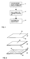
- Fig. 1 illustrates a method according to the invention for implementing EMI shielding.
- the conductive layer in the conductive polymer/insulating film combination according to the method is a PANI/CSA film manufactured by dissolving PANI/CSA in m-cresol.
- the conductive film is produced on top of the insulating film e.g. as follows: a drop of liquid conductive material is placed on the centre of the insulating film which is rapidly spinned whereupon the conductive material is spread by the centrifugal force on the surface of the insulating film thus forming a conductive material film, block 11. This method is called centrifugal spreading, or spinning.
- the revolution speed used in spinning is typically 1000 to 2000 rpm.
- a spinned PANI/CSA film is approximately 1 ⁇ m and the conductivity is 100 S/cm. approximately.
- Spraying and dipping are methods suitable for large areas and applicable as continuous processes. In these methods. a conductive polymer dissolved in a suitable solvent, such as m-cresol, is spread on the surface of the insulating layer.
- the insulating film is advantageously one of the flexible plastic films mentioned above having good electrical insulating properties and at the same time good solvent resistance.
- glue is spread, if necessary, on the surface of the insulating film to attach the film to the electronic means unless the insulating film is already coated with glue, block 12.
- the conductive layer may also be under the insulating film so that glue is spread on top of it.
- This structure can be used when the areas to be shielded in the electronic means are insulating. The advantage of this structure is that the conductive layer is protected against the environment. A corresponding protection layer can be used in other film combinations, too, if necessary.
- the resulting combination of conductive and insulating film is attached to the electronic means advantageously using heat and low-pressure treatment, block 13.
- the film is placed on top of the electronic means and heated in order to make it mouldable.
- a vacuum is produced below the film, whereby the film is pressed against the surface of the electronic means and is moulded, where necessary, to topographically follow the contours of the surface of the electronic means.
- Due to the simultaneous heat and vacuum treatment the film is shaped and attached, by means of the glue spread on the insulating film, to the surface of the electronic means.
- the glue is advantageously elastic so that temperature changes will not result in tension between the film and the electronic means.
- the insulating film may also be made of plastic that shrinks when heated, such as polyethene. Such a tube-like film is suitable for shielding equipment, connections and cables in the manner of a shrink sleeve.
- Fig. 2 shows the shielding structure in different phases of the method illustrated in Fig. 1.
- Film 21 consists of an insulating film 20 which has a layer of glue 24 on its underside.
- Film 23 includes a conductive film 22 spread on top of film 21 mentioned above.
- the resulting film 28 is attached onto the surface of an electronic means comprising a printed circuit board 26 and components 27 inserted on the printed circuit board.
- PANI DBSA Another conductive film material that can be used in the arrangement according to the invention is PANI DBSA.
- PANI DBSA is solidified in about 200 °C into a solid film which can be hot-moulded in about 100 °C so as to form a combination with an insulating film. This method has the advantage that the insulating film need not be capable of standing the 200 °C temperature of the solidifying process.
- the thickness of a solidified PANI, DBSA film is ⁇ 70 ⁇ m and conductivity ⁇ 2 S/cm.
- the PANI/DBSA film can also be made of a PANI + DBSA blend using extrusion moulding.
- Fig. 3 shows a shielding arrangement according to the invention in which a PANI/CSA film 38 has been spin-coated on a 100- ⁇ m polycarbonate film 37.
- This two-layer film has been attached onto the surface of an electronic means by means of vacuum or heat treatment or the combination of the two.
- the films in Fig. 3 are shown thicker than they really are with respect to the electronic means and the components inserted in it.
- the layers in the film must be capable of moulding themselves according to the surface topography of the device shielded.
- the PANI/CSA insulating film combination can be attached with a separate layer of glue (not shown) to the surface of the electronic means.
- the electronic means shown in Fig. 3 comprises a printed circuit board 30 with wired 32 components 31, surface-mounted 34 components 33, and encapsulated 36 components 35.
- the method of the invention can also be used to produce a multilayer structure in which the conductive polymer and insulating film layers alternate.
- the advantage of the multilayer structure is a better shielding efficiency, a limiting factor is possibly poorer mouldability as the thickness grows.
- the film could be placed on the surface of the insulating film by means of silk screen printing technology.
- the conductive polymer layer For the conductive polymer layer to serve as an effective EMI shield it must be electrically connected to the electronic means, advantageously to a constant potential, such as the ground plane, in the electronic means.
- the most important requirement for a reliable electric contact is its ohmic quality, in other words the contact resistance must be small in comparison with the resistance of the conductive polymer film and the metal-polymer junction must not restrict the flow of current. In principle.
- the coupling type is determined on the basis of the work functions ( ⁇ m , ⁇ p ) of the material used for contacting and the conductive polymer film in a manner such that metals like aluminium and indium that have a small work function (e ⁇ AI ⁇ 4.2 eV, e ⁇ In ⁇ 4.1 eV) form a rectifying contact, and metals like gold (e ⁇ Au ⁇ 5.3 eV) and graphite (e ⁇ m ⁇ 5.5 eV) that have a high work function form an ohmic contact usually in a p-type conductive polymer film.
- Metals that have a high work function also have the advantage that they are not easily oxidized and so the contact is more stable.
- the contacting materials are graphite paste and silver paint (e ⁇ Ag ⁇ 4.6 eV) which do not require heat treatment in order to dry up and do not contain solvents detrimental to the conductive polymer film.
- Fig. 4 shows two embodiments according to the invention for electrically connecting a conductive polymer layer to the ground potential of a printed circuit board assembly serving as an electronic means.
- a conductor area 44 coupled to the ground potential plane in the middle of the multilayer printed circuit board by means of a lead-through (not shown), for example.
- a hole is made in the films at said conductor area by means of a laser, for example.
- the hole is completely or in part filled with a conductive layer 45 consisting of a drop or sprayed intrinsically conductive polymer, a graphite paste or a polymer containing silver.
- a projection 46 which may be a sharp spike, is attached perpendicularly to the printed circuit board to the grounding point.
- the spikes penetrate the shielding film 42, 43 and extend through the conductive polymer film.
- the conductive polymer 43 is electrically connected by means of a conductive substance 47, such as a graphite paste or a polymer containing silver, to said spikes at and around the edges of the hole formed in the penetration.
- a conductive substance 47 such as a graphite paste or a polymer containing silver
- Another embodiment of the invention comprises a method where a shielding film is first attached to the surface of an electronic means using e.g. a method described above and then a conductive film is sprayed on the surface or areas where there are holes formed in the insulating film for ground connections to the printed circuit board.
- Fig. 5 shows a cross section of a shielding arrangement according to the invention where the shield is also used for forming a capacitor and a resistor.
- the shield is also used for forming a capacitor and a resistor.
- the conductive films are connected electrically to grounding pads 516 and 518 with electrical connections 505 and 515.
- the first area consists of insulating film areas 507 and 509 and conductive film areas 506, 508.
- the first conductive film area 506 is connected electrically to a ground contact pad 516 with an electrical connection 505.
- the second conductive film area 508 is connected electrically to a signal pad 517 with an electrical connection 510.
- the electrical connections between film areas and pads are preferably made by applying intrinsically conductive polymer to the edges of cut lines or holes.
- the conductive film areas 506 and 508 are formed by e.g. laser or acid treatment in such a way that there will be no electrical short circuit from a conductive film area to the opposite electrical connection of the formed capacitor.
- the second separated area consists of conductive films 511, 512 and insulating films 512, 514.
- the first conductive film area 511 is connected to the signal pad 517 and grounding pad 518 from its ends.
- the resistance of the resistor can be adjusted to a suitable value by forming the conductive film area into a defined pattern with laser or acid pen. This is due to the fact that applying heat and acid to the conductive film reduces or destroys its conductivity.
- the second conductive film area 513 is isolated from both electrical contacts, so it does not affect the resistivity of the resistor. A resistor can thus also be made with a shield that has only one conductive film layer.
- the shielding methods according to the invention have several advantages over the known methods.
- the method requires only a few steps and the necessary steps can be made automatic so that the costs of shielding remain low.
- the shielding is tight since the shield is continuous and has no holes or openable joints.
- a thin film does not substantially reduce heat conduction from the electronic means.
- the shielding film can be made transparent or translucent whereby it is possible to see the components of the electronic means and their markings through the shielding film. Therefore, the method can be applied to electronic means that contain display components such as light-emitting diodes indicating operational status, for example.
- the method and arrangement according to the invention can be advantageously applied to electronic means, such as printed circuit board assemblies, where the differences in surface height are a few millimetres at the most. If the differences in height are considerable, the film will stretch at such locations and the shielding effect of the film will be reduced.
- the most advantageous EMI shielding method according to the invention is one where the highest operating frequencies of the electronic means to be shielded are 100 MHz to 1 GHz at the most. Then the film will act as an effective EMI shield.
- Applicable devices include telecommunication terminals, such as mobile stations, and computer equipment and measuring instruments.
Abstract
The invention relates to a method and an arrangement for shielding an electronic means (40, 41) against external electromagnetic interference on one hand, and preventing the electronic means from interfering with closeby electric devices on the other hand. According to the invention, a shielding film (42, 43) with one or more layers is formed comprising one or more intrinsically conductive polymer films (43) and one or more insulating films (42). The shielding film (42, 43) so formed is attached to the surface of the electronic means (40, 41) using a heat treatment or a vacuum treatment or the combination of the two and, if necessary, a separate layer of glue. The invention also relates to a method for electrically connecting (44, 45, 46, 47) the intrinsic polymer layer (43) reliably to the electronic means (40, 41). The invention further relates to a method for using the electromagnetic shield to form capacitors and resistors for the electronic means.
Description
- The invention relates to a method for shielding an electronic means against external electromagnetic radiation on one hand, and preventing the electromagnetic radiation of the electronic means from interfering with closeby apparatuses on the other hand. The electronic means may be an electronic apparatus, for example, or a unit, such as a printed circuit board assembly. in an electronic apparatus.
- Electromagnetic interference (EMI) shielding of electric equipment is traditionally based on the use of either metal equipment cases or plastic cases coated with a metal layer. In addition, methods are known for manufacturing cases of a conductive plastic composite where conductive particles, such as carbon black, carbon fibres, metal fibres or metal flakes are mixed with the insulating plastic.
- Disadvantages of a metal case include its weight and the high price caused by numerous machining steps. Also the coating of a plastic case with a metal layer includes many steps and is therefore uneconomic. The disadvantage of methods based on conductive plastic composites is uneven distribution of conductive particles which leaves unshielded spots in the case. Furthermore, in all the above methods it is difficult to make the EMI shielding tight because of holes and joints in the case.
- At the printed circuit board (PCB) level, the EMI shielding is usually realised by a multilayer PCB (internal ground layers) or by a polymer composite containing conductive metal particles and spread by means of silk screen printing. Reference [1] discloses such a method based on a polymer composite which, however, is restricted only to shield wirings on a PCB. Since components and their coupling areas constitute a great part of the area of an electronic means, the shielding provided by this method is insufficient. Nor does a multilayer PCB shield the whole electronic means and the surface-mounted or other components on it.
- Reference [2] discloses a method in which a non-conductive substrate material is coated using a chemical copper plating method. In the method, the part to be coated is submerged in a chemical bath, so usually the method cannot be applied to an electronic means because it might cause damage to the components and because the metal coating might cause a short circuit.
- Reference [3] discloses a method in which the conductive shell (metal. for example) of a component is coupled to the ground plane of the equipment case. Then, separate shielding cases must be provided for the components and, in addition, the inner surface of the equipment case must be provided with a conductive layer. The extra cost of this method caused by the many steps is too high for the manufacturing of most electronic devices.
- In addition. a method is known from reference [4], wherein conductive polyaniline is used to absorb electromagnetic radiation. The absorber can be used for electromagnetic absorption in the IR, visible light, UV, radar or microwave range. However, said patent document discloses no technical implementation for the EMI shielding of an electronic means.
- An object of the invention is to eliminate the disadvantages of known EMI shielding methods by providing a new kind of method for the EMI shielding of an electronic means. In the method according to the invention, electromagnetic shielding is produced using a conductive film material placed near the surface of an electronic means. The conductive film is isolated from the electronic means by an insulator film. By using e.g. an intrinsically conductive polymer (ICP) such as polyaniline according to the invention, known solutions and methods can be implemented more advantageously and near to the surface of the electronic means. The method is not only an economic but also a quick way of shielding an electronic means. The method is also suitable for an electronic assembly where the coupling regions of components are unshielded because the insulator film prevents short-circuits. Another object of the invention is to provide a method for electrically connecting a conductive film material to an electronic means, advantageously to its ground potential. The inventive solution can also be used for forming capacitors and resistors for the circuits of electronic means.
- The method according to the invention is characterized in that said electronic means is coated with an electrically insulating material and said insulating material is coated with an electrically conductive material. The arrangement according to the invention is characterized in that it comprises at least one electrically conductive film to shield against electromagnetic radiation and at least one electrically insulating film to insulate said electrically conductive film from electrically conductive parts in the electronic means.
- The invention is described with reference to the accompanying drawing, where
- Fig. 1 shows in flow chart format the manufacturing steps of a shielding method according to the invention,
- Fig. 2 shows the shielding films after the manufacturing steps according to Fig. 1,
- Fig. 3 is a cross section of a shielding arrangement according to the invention for a printed circuit board assembly and
- Fig. 4 is a cross section of conductive film grounding arrangements according to the invention.
- Fig. 5 is a cross section of a shielding arrangement according to the invention where the shield is also used for forming a capacitor and a resistor.
- We will next discuss the EMI shielding characteristics of the conductive film used in the invention in order to illustrate the operating principles of the invention. Then we will disclose in more detail a shielding method according to the invention by means of Figs. 1 and 2, and a shielding arrangement according to the invention by means of Fig. 3. Finally, we will disclose an implementation according to the invention to ground an EMI shield, referring to Fig. 4.
- The EMI shielding capability of an intrinsically conductive polymer film and other films made of a conductive material is based on the fact that electromagnetic radiation is reflected from a conductive surface while the proportion of absorption losses and losses caused by multiple reflections within the material is small. The most significant parameters in estimating the shielding capability are the conductivity σ and thickness d of the conductive coating, frequency f of the interfering radiation, and the distance r between the interfering source and the shielding layer which determines whether we are dealing with a near field or with a far field. One quantity that is frequently used in estimating the shielding capability in a far field is the depth of penetration δ, which describes the distance in the shielding layer in which the intensity of interfering electromagnetic radiation is attenuated to the 1/eth part of the original value. The shielding effect is discussed in further detail in document [6] which contains the formula

- A formula [6] has been proven for reflection losses Re in an electric near field:

- In the method and arrangement according to the invention, the conductive film is advantageously made of an intrinsically conductive polymer. The basic method to make the polymer conductive is similar to that used for traditional semiconductors, i.e. doping. The impurity molecules or atoms added to the polymer enable hole conduction or electron conduction.
- The impurity ion attached to the polymer chain in the doping process causes a little but significant change in the relationship between the polymer chain atoms. This change facilitates the generation of different types of defects for example solitons, polarons and bipolarons and they are formed near the impurity ions. So, the doping mechanisms for traditional semiconductors and for conductive polymers on the other hand are clearly different in that in the case of conductive polymers the impurity molecules never replace the atoms in the polymer chain like in the case of silicon doping, for example, but bound adjacent to the chains they act as donors or acceptors of electrons.
- The most extensively studied conductive polymer materials have been polyacetylene, polytiophene, polypyrrole, polyparaphenylene, polyaniline and their modifications. Polyaniline is of special interest because it has good stability characteristics combined to a relatively high conductivity level. Polyaniline can also be solution processed in conductive state without substantially changing the structure and conduction capability of the polymer. Polyaniline is further discussed in reference [5].
- The conductive polymer film used in connection with the method according to the invention may be e.g.
- polyaniline which is doped through protonation using a functional protonic acid, such as dodecyl benzene sulphonic acid (DBSA) or camphor sulphonic acid (CSA), thereby improving the solubility of the conductive polymer in some organic solvents (e.g. PANI/CSA dissolves in m-cresol), and in the case of PANI/DBSA it is possible to make conductive blends in which polyaniline is the conductive constituent,
- solution-mouldable polyalkyltiophene which is post-doped or
- polypyrrole manufactured through chemical polymerization.
- The insulating film used in the method according to the invention advantageously meets the following requirements:
- the insulating film together with the conductive polymer film layer is topographically moulded on the surface of the electronic means,
- the insulating film is a good electrical insulator,
- the insulating film has a good solvent resistance if the conductive polymer solution is spread on the surface of the insulating film,
- the conductive polymer adheres well to the insulating film, and
- the insulating film stands manufacturing and coupling stages and retains its characteristics in the operating conditions of the electronic means.
- In practice, the thickness of the insulating film may be about 20 to 300 µm, but to make the handling of the film easier the thickness is advantageously 50 to 150 µm.
- Insulating film materials that meet the above requirements include polycarbonate (manufactured by BAYER/Makrofol), polyurethane Walopur® (manufactured by Wolff Walsrode AG) and polyvinyl fluoride Tedlar® (manufactured by Du Pont).
- Fig. 1 illustrates a method according to the invention for implementing EMI shielding. The conductive layer in the conductive polymer/insulating film combination according to the method is a PANI/CSA film manufactured by dissolving PANI/CSA in m-cresol. The conductive film is produced on top of the insulating film e.g. as follows: a drop of liquid conductive material is placed on the centre of the insulating film which is rapidly spinned whereupon the conductive material is spread by the centrifugal force on the surface of the insulating film thus forming a conductive material film, block 11. This method is called centrifugal spreading, or spinning. The revolution speed used in spinning is typically 1000 to 2000 rpm. The thickness of a spinned PANI/CSA film is approximately 1 µm and the conductivity is 100 S/cm. approximately. Spraying and dipping are methods suitable for large areas and applicable as continuous processes. In these methods. a conductive polymer dissolved in a suitable solvent, such as m-cresol, is spread on the surface of the insulating layer.
- The insulating film is advantageously one of the flexible plastic films mentioned above having good electrical insulating properties and at the same time good solvent resistance. After the formation of the conductive polymer layer glue is spread, if necessary, on the surface of the insulating film to attach the film to the electronic means unless the insulating film is already coated with glue, block 12. The conductive layer may also be under the insulating film so that glue is spread on top of it. This structure can be used when the areas to be shielded in the electronic means are insulating. The advantage of this structure is that the conductive layer is protected against the environment. A corresponding protection layer can be used in other film combinations, too, if necessary.
- The resulting combination of conductive and insulating film is attached to the electronic means advantageously using heat and low-pressure treatment, block 13. In the treatment, the film is placed on top of the electronic means and heated in order to make it mouldable. At the same time, a vacuum is produced below the film, whereby the film is pressed against the surface of the electronic means and is moulded, where necessary, to topographically follow the contours of the surface of the electronic means. Due to the simultaneous heat and vacuum treatment the film is shaped and attached, by means of the glue spread on the insulating film, to the surface of the electronic means. The glue is advantageously elastic so that temperature changes will not result in tension between the film and the electronic means. The insulating film may also be made of plastic that shrinks when heated, such as polyethene. Such a tube-like film is suitable for shielding equipment, connections and cables in the manner of a shrink sleeve.
- Fig. 2 shows the shielding structure in different phases of the method illustrated in Fig. 1.
Film 21 consists of an insulatingfilm 20 which has a layer ofglue 24 on its underside.Film 23 includes aconductive film 22 spread on top offilm 21 mentioned above. Finally, the resultingfilm 28 is attached onto the surface of an electronic means comprising a printedcircuit board 26 andcomponents 27 inserted on the printed circuit board. - Another conductive film material that can be used in the arrangement according to the invention is PANI DBSA. PANI DBSA is solidified in about 200 °C into a solid film which can be hot-moulded in about 100 °C so as to form a combination with an insulating film. This method has the advantage that the insulating film need not be capable of standing the 200 °C temperature of the solidifying process. The thickness of a solidified PANI, DBSA film is ∼70 µm and conductivity ∼2 S/cm. The PANI/DBSA film can also be made of a PANI + DBSA blend using extrusion moulding.
- Fig. 3 shows a shielding arrangement according to the invention in which a PANI/
CSA film 38 has been spin-coated on a 100-µm polycarbonate film 37. This two-layer film has been attached onto the surface of an electronic means by means of vacuum or heat treatment or the combination of the two. Please notice that in order to better illustrate the film structures the films in Fig. 3 are shown thicker than they really are with respect to the electronic means and the components inserted in it. For the attachment by low-pressure to be successful the layers in the film must be capable of moulding themselves according to the surface topography of the device shielded. As in the case above, the PANI/CSA insulating film combination can be attached with a separate layer of glue (not shown) to the surface of the electronic means. The electronic means shown in Fig. 3 comprises a printedcircuit board 30 with wired 32components 31, surface-mounted 34components 33, and encapsulated 36components 35. - The method of the invention can also be used to produce a multilayer structure in which the conductive polymer and insulating film layers alternate. The advantage of the multilayer structure is a better shielding efficiency, a limiting factor is possibly poorer mouldability as the thickness grows.
- It is conceivable that in addition to the manufacturing methods described above the film could be placed on the surface of the insulating film by means of silk screen printing technology.
- For the conductive polymer layer to serve as an effective EMI shield it must be electrically connected to the electronic means, advantageously to a constant potential, such as the ground plane, in the electronic means. The most important requirement for a reliable electric contact is its ohmic quality, in other words the contact resistance must be small in comparison with the resistance of the conductive polymer film and the metal-polymer junction must not restrict the flow of current. In principle. the coupling type is determined on the basis of the work functions (φm, φ p) of the material used for contacting and the conductive polymer film in a manner such that metals like aluminium and indium that have a small work function (eφAI ≈ 4.2 eV, eφIn ≈ 4.1 eV) form a rectifying contact, and metals like gold (eφAu ≈ 5.3 eV) and graphite (eφm ≈ 5.5 eV) that have a high work function form an ohmic contact usually in a p-type conductive polymer film. Metals that have a high work function also have the advantage that they are not easily oxidized and so the contact is more stable.
- In the implementation method discussed in this invention the contacting materials are graphite paste and silver paint (eφAg ≈ 4.6 eV) which do not require heat treatment in order to dry up and do not contain solvents detrimental to the conductive polymer film.
- Fig. 4 shows two embodiments according to the invention for electrically connecting a conductive polymer layer to the ground potential of a printed circuit board assembly serving as an electronic means. In the first embodiment there is on the surface of a multilayer printed circuit board 40 a
conductor area 44 coupled to the ground potential plane in the middle of the multilayer printed circuit board by means of a lead-through (not shown), for example. When the combination of the insulatingfilm 42 andconductive film 43 has been attached to the surface of the printedcircuit board assembly conductive layer 45 consisting of a drop or sprayed intrinsically conductive polymer, a graphite paste or a polymer containing silver. - In the second embodiment a
projection 46, which may be a sharp spike, is attached perpendicularly to the printed circuit board to the grounding point. As the shielding film is attached the spikes penetrate the shieldingfilm conductive polymer 43 is electrically connected by means of aconductive substance 47, such as a graphite paste or a polymer containing silver, to said spikes at and around the edges of the hole formed in the penetration. When using this grounding method one must bear in mind that the grounding spikes must not penetrate the films during the vacuum treatment because then the attachment of the film would be incomplete. Therefore, with this grounding method it is advantageous to use mechanical pressing instead of the vacuum treatment to attach the film. - With the multilayer structure it is advantageous to connect all the conductive planes of the structure to the ground potential by means of a conductive contact. This can be arranged using the grounding methods described above in a manner such that the
conductive substance 45 forms a contact with the edges of the conductive planes in the hole. - Another embodiment of the invention comprises a method where a shielding film is first attached to the surface of an electronic means using e.g. a method described above and then a conductive film is sprayed on the surface or areas where there are holes formed in the insulating film for ground connections to the printed circuit board.
- Fig. 5 shows a cross section of a shielding arrangement according to the invention where the shield is also used for forming a capacitor and a resistor. There is a shield with two layers of dielectric insulating
film conductive film circuit board 500. The conductive films are connected electrically to groundingpads electrical connections - There are two areas that are separated from the shielding film. The first area consists of insulating
film areas 507 and 509 andconductive film areas conductive film area 506 is connected electrically to aground contact pad 516 with anelectrical connection 505. The secondconductive film area 508 is connected electrically to asignal pad 517 with anelectrical connection 510. thus the capacitance that is formed between theconductive film areas ground pad 516 and thesignal pad 517. The electrical connections between film areas and pads are preferably made by applying intrinsically conductive polymer to the edges of cut lines or holes. Theconductive film areas - The second separated area consists of
conductive films films 512, 514. The firstconductive film area 511 is connected to thesignal pad 517 andgrounding pad 518 from its ends. Thus there is a resistor formed between the two pads. The resistance of the resistor can be adjusted to a suitable value by forming the conductive film area into a defined pattern with laser or acid pen. This is due to the fact that applying heat and acid to the conductive film reduces or destroys its conductivity. The second conductive film area 513 is isolated from both electrical contacts, so it does not affect the resistivity of the resistor. A resistor can thus also be made with a shield that has only one conductive film layer. - As was stated earlier, the shielding methods according to the invention have several advantages over the known methods. The method requires only a few steps and the necessary steps can be made automatic so that the costs of shielding remain low. In addition. the shielding is tight since the shield is continuous and has no holes or openable joints. Furthermore, a thin film does not substantially reduce heat conduction from the electronic means.
- By means of the manufacturing methods described above the shielding film can be made transparent or translucent whereby it is possible to see the components of the electronic means and their markings through the shielding film. Therefore, the method can be applied to electronic means that contain display components such as light-emitting diodes indicating operational status, for example.
- The method and arrangement according to the invention can be advantageously applied to electronic means, such as printed circuit board assemblies, where the differences in surface height are a few millimetres at the most. If the differences in height are considerable, the film will stretch at such locations and the shielding effect of the film will be reduced.
- The most advantageous EMI shielding method according to the invention is one where the highest operating frequencies of the electronic means to be shielded are 100 MHz to 1 GHz at the most. Then the film will act as an effective EMI shield.
- The invention described above can be advantageously applied to various electronic means whose electromagnetic radiation may interfere with other electronic means or whose operation may be disturbed by electromagnetic radiation from the environment. Applicable devices include telecommunication terminals, such as mobile stations, and computer equipment and measuring instruments.
- Above it was described a few embodiments of the method according to the invention. Naturally, the principle according to the invention can be modified within the scope of the claims e.g. as regards implementation details and fields of use. Especially, the values mentioned in the descriptions of the embodiments of the invention are given as examples only.
-
- [1] Carr, J.D., Hertz, A.D. and Tribbey, D.A., In situ RF shield for printed circuit board, U.S. Patent 5,177,324
- [2] Waggoner, J., Method of using a shielding means to attenuate electromagnetic radiation in the radio frequency range, U.S. 4,514,586
- [3] Yokoyama, Y., Portable radio communication apparatus unnecessitating shielding case, EP 0 522 538
- [4] Espstein et al., Electromagnetic radiation absorbers and modulators comprising polyaniline, U.S. 5,294,694
- [5] Andreatta, A. et al., Electrically conductive polyaniline, U.S. 5,196,144
- [6] Williams, T., EMC for Product Designers, Butterworth-Heinemann Ltd. 1992, 255 pp.
Claims (21)
- A method of providing electromagnetic shielding for an electronic means (26, 40, 41), characterized in that said electronic means is coated with an electrically insulating film (21, 42) and said electrically insulating film is coated with an electrically conductive film (22, 43).
- The method of claim 1, characterized in that the electrically conductive material is made to have such a thickness that the shielding effect is substantially based on reflection.
- The method of claim 1 or 2, characterized in that a liquid conductive material (22) is spread by spinning, spraying or dipping onto the surface of said electrically insulating film (21) in order to produce said electrically conductive film.
- The method of claim 1, 2 or 3, characterized in that said conductive film material (22) is an intrinsic PANI/CSA polymer film.
- The method of claim 1 or 2, characterized in that a liquid conductive material is solidified into a solid conductive film which is attached to an insulating film using hot moulding.
- The method of claim 5, characterized in that said conductive film material (43) is an intrinsic PANI/DBSA polymer film.
- The method of any one of the preceding claims, characterized in that said insulating film material (20, 42) is a polycarbonate, polyurethane or polyvinyl fluoride.
- The method of any one of the preceding claims, characterized in that to attach said insulating film (20, 42) to the surface of an electronic device said insulating film material is coated with glue, thermally treated and vacuum treated.
- The method of any one of the preceding claims, characterized in that said conductive film (43) is electrically connected to said electronic means (40, 41).
- The method of claim 9, characterized in that to electrically connect the conductive film (43) to the electronic means (40, 41)- a conductor area (44) is formed on the surface of the electronic means,- a hole is made at said conductor area (44) in the shielding film comprising one or more insulating films (42) and one or more conductive films (43), and- the conductive film or films are connected through said hole to the conductor area (44) by means of an electrically conductive substance (45).
- The method of claim 9, characterized in that to connect the conductive film to the electronic means (40. 41)- the electronic means is provided with an electrically conductive projection (46) perpendicular to the surface of the electronic means,- said insulating film (42) and conductive film (43) are attached to the surface of the electronic means in a manner such that said projection (46) penetrates said films and- said projection (46) is connected to the conductive film (43) through an electrically conductive substance (47).
- The method of claim 10 or 11, characterized in that said electrically conductive substance (47) is an intrinsically conductive polymer, a graphite paste or a polymer containing silver.
- An arrangement for electromagnetically shielding an electronic means (40, 41), characterized in that it comprises at least one electrically conductive film (43) to shield against electromagnetic radiation and at least one electrically insulating film (42) to insulate said electrically conductive film (43) from the electrically conductive parts in the electronic means.
- The arrangement of claim 13, characterized in that said insulating film (42) is attached to the surface of said electronic means and said conductive film (43) is attached to the surface of said insulating film (42).
- The arrangement of claim 13 or 14, characterized in that said conductive film (43) is an intrinsically conductive polymer film.
- The arrangement of any one of claims 13 to 15, characterized in that the arrangement comprises means to electrically connect said conductive film (43) to said electronic means (40, 41).
- The arrangement of claim 16, characterized in that said means for the electric connection comprises a conductor area (44) on the surface of the electronic means, an insulating film (42) and a conductive film (43) attached to the surface of the electronic means, which have a hole at said conductor area (44), and a conductive substance (45) which electrically connects the edge of the hole in the conductive film to said conductor area (44).
- The arrangement of any one of claims 13 to 17, characterized in that the arrangement comprises at least two insulator films and at least two conductive films which form a layered structure in which said insulator films and said conductive films alternate.
- The arrangement of claim 18, characterized in that the arrangement comprises two electrically separated areas (506, 507) of conductive film at the opposite surfaces of the insulator film, and said conductive areas are connected electrically to said electronic means to form a capacitor in an electronic circuit.
- The arrangement of any one of claims 13 to 18, characterized in that the arrangement comprises an electrically separated area (511) of conductive film, and two points of said conductive area are connected electrically to said electronic means to form a resistor.
- The use of the method of any one of claims 1 to 12 or the arrangement of any one of claims 13 to 20 in a mobile communication device.
Applications Claiming Priority (2)
| Application Number | Priority Date | Filing Date | Title |
|---|---|---|---|
| FI956226 | 1995-12-22 | ||
| FI956226A FI956226A (en) | 1995-12-22 | 1995-12-22 | Method and apparatus for electromagnetic protection of an electromagnetic agent |
Publications (1)
| Publication Number | Publication Date |
|---|---|
| EP0781085A1 true EP0781085A1 (en) | 1997-06-25 |
Family
ID=8544602
Family Applications (1)
| Application Number | Title | Priority Date | Filing Date |
|---|---|---|---|
| EP96660099A Withdrawn EP0781085A1 (en) | 1995-12-22 | 1996-12-18 | Method and arrangement for electromagnetically shielding an electronic means |
Country Status (3)
| Country | Link |
|---|---|
| US (1) | US6110563A (en) |
| EP (1) | EP0781085A1 (en) |
| FI (1) | FI956226A (en) |
Cited By (9)
| Publication number | Priority date | Publication date | Assignee | Title |
|---|---|---|---|---|
| US5867371A (en) * | 1997-09-29 | 1999-02-02 | Ericsson Inc. | Cover member for sealed circuit board assembly |
| EP1178712A2 (en) * | 2000-07-31 | 2002-02-06 | The Boeing Company | Structure with blended polymer conformal coating of controlled electrical resistivity |
| EP1235198A2 (en) * | 2001-02-21 | 2002-08-28 | Siemens Aktiengesellschaft | Cover plate for a display system |
| WO2003015487A1 (en) * | 2001-08-11 | 2003-02-20 | Ubinetics Limited | A method of providing radio frequency screening for electric components |
| WO2003092347A1 (en) | 2002-04-23 | 2003-11-06 | Nec Corporation | Electromagnetically shielded circuit device and shielding method therefor |
| US7005573B2 (en) | 2003-02-13 | 2006-02-28 | Parker-Hannifin Corporation | Composite EMI shield |
| US7326862B2 (en) | 2003-02-13 | 2008-02-05 | Parker-Hannifin Corporation | Combination metal and plastic EMI shield |
| WO2021106455A1 (en) * | 2019-11-29 | 2021-06-03 | 日立Astemo株式会社 | Electronic control device |
| DE102020213787A1 (en) | 2020-10-29 | 2022-05-05 | Continental Automotive Gmbh | Electronic module and method for manufacturing such an electronic module |
Families Citing this family (26)
| Publication number | Priority date | Publication date | Assignee | Title |
|---|---|---|---|---|
| US5811050A (en) * | 1994-06-06 | 1998-09-22 | Gabower; John F. | Electromagnetic interference shield for electronic devices |
| US6501945B1 (en) * | 1999-02-05 | 2002-12-31 | Benq Corporation | Cellular phone with an insulating envelope for preventing leakage of electromagnetic radiation |
| JP3183280B2 (en) * | 1999-03-19 | 2001-07-09 | 日本電気株式会社 | Electrodes and batteries |
| US6631555B1 (en) * | 2000-02-08 | 2003-10-14 | Cardiac Pacemakers, Inc. | Method of thin film deposition as an active conductor |
| US6768654B2 (en) * | 2000-09-18 | 2004-07-27 | Wavezero, Inc. | Multi-layered structures and methods for manufacturing the multi-layered structures |
| US6515352B1 (en) * | 2000-09-25 | 2003-02-04 | Micron Technology, Inc. | Shielding arrangement to protect a circuit from stray magnetic fields |
| US6515222B2 (en) * | 2001-02-05 | 2003-02-04 | Motorola, Inc. | Printed circuit board arrangement |
| US6743975B2 (en) * | 2001-03-19 | 2004-06-01 | Hewlett-Packard Development Company, L.P. | Low profile non-electrically-conductive component cover for encasing circuit board components to prevent direct contact of a conformal EMI shield |
| US6900383B2 (en) * | 2001-03-19 | 2005-05-31 | Hewlett-Packard Development Company, L.P. | Board-level EMI shield that adheres to and conforms with printed circuit board component and board surfaces |
| US20050095410A1 (en) * | 2001-03-19 | 2005-05-05 | Mazurkiewicz Paul H. | Board-level conformal EMI shield having an electrically-conductive polymer coating over a thermally-conductive dielectric coating |
| US6828012B2 (en) * | 2001-04-10 | 2004-12-07 | Cory L. Groft | Slab shield insulation |
| US20050118408A1 (en) * | 2001-04-10 | 2005-06-02 | Groft Cory L. | Multi-layer insulation |
| US6603080B2 (en) | 2001-09-27 | 2003-08-05 | Andrew Corporation | Circuit board having ferrite powder containing layer |
| KR100477019B1 (en) * | 2002-08-30 | 2005-03-17 | 에스엔케이폴리텍(주) | High polymer microcellular foam conductive gaskets and method for preparing thereof |
| EP1561237A2 (en) * | 2002-08-14 | 2005-08-10 | Honeywell International, Inc. | Method and apparatus for reducing electromagnetic emissions from electronic circuits |
| US7366554B2 (en) * | 2004-08-09 | 2008-04-29 | Sony Ericsson Mobile Communications Ab | Reduction of near field E-M scattering using high impedance coating materials |
| US7491899B2 (en) * | 2005-10-06 | 2009-02-17 | Laird Technologies, Inc. | EMI shields and related manufacturing methods |
| US8004860B2 (en) * | 2006-08-29 | 2011-08-23 | Texas Instruments Incorporated | Radiofrequency and electromagnetic interference shielding |
| US7504592B1 (en) | 2007-08-31 | 2009-03-17 | Laird Technologies, Inc. | Electromagnetic interference shields and related manufacturing methods |
| US8276268B2 (en) * | 2008-11-03 | 2012-10-02 | General Electric Company | System and method of forming a patterned conformal structure |
| CN103087574B (en) * | 2011-10-27 | 2014-12-10 | 比亚迪股份有限公司 | Electromagnetic shielding filling material and preparation method thereof, and electromagnetic shielding paint |
| WO2013107920A1 (en) | 2012-01-16 | 2013-07-25 | Nokia Corporation | Method and shielding units for inductive energy coils |
| JP5903668B2 (en) * | 2013-02-21 | 2016-04-13 | パナソニックIpマネジメント株式会社 | Component mounting apparatus and component mounting method |
| JP2014160788A (en) | 2013-02-21 | 2014-09-04 | Panasonic Corp | Component mounting apparatus and component mounting method |
| US9357683B2 (en) * | 2014-09-26 | 2016-05-31 | Laird Technologies, Inc. | Electromagnetic interference (EMI) shielding apparatus including electrically-conductive foam |
| US10651408B2 (en) * | 2017-02-14 | 2020-05-12 | International Business Machines Corporation | Selenium-fullerene heterojunction solar cell |
Citations (10)
| Publication number | Priority date | Publication date | Assignee | Title |
|---|---|---|---|---|
| FR2151665A5 (en) * | 1971-09-08 | 1973-04-20 | Matra Engins | |
| US4514586A (en) | 1982-08-30 | 1985-04-30 | Enthone, Inc. | Method of using a shielding means to attenuate electromagnetic radiation in the radio frequency range |
| WO1991005979A1 (en) * | 1989-10-19 | 1991-05-02 | The Ohio State University Research Foundation | Polyaniline compositions, process for their preparation and uses thereof |
| GB2248971A (en) * | 1990-10-15 | 1992-04-22 | Nippon Cmk Kk | Shielded printed wiring board |
| US5177324A (en) | 1991-08-19 | 1993-01-05 | Motorola, Inc. | In situ RF shield for printed circuit board |
| EP0522538A2 (en) | 1991-07-11 | 1993-01-13 | Nec Corporation | Portable radio communication apparatus unnecessitating shielding case |
| US5196144A (en) | 1988-10-31 | 1993-03-23 | The Regents Of The University Of California | Electrically conductive polyaniline |
| US5294755A (en) * | 1989-03-15 | 1994-03-15 | Nippon Cmk Corp. | Printed wiring board having shielding layer |
| US5294694A (en) | 1988-05-13 | 1994-03-15 | The Ohio State University Research Foundation | Electromagnetic radiation absorbers and modulators comprising polyaniline |
| WO1995028822A1 (en) * | 1994-04-18 | 1995-10-26 | Motorola Inc. | Conformal shield and method for forming same |
Family Cites Families (22)
| Publication number | Priority date | Publication date | Assignee | Title |
|---|---|---|---|---|
| US5407699A (en) * | 1984-06-08 | 1995-04-18 | The B. F. Goodrich Company | Electrically conductive pyrrole polymers |
| US5017420A (en) * | 1986-10-23 | 1991-05-21 | Hoechst Celanese Corp. | Process for preparing electrically conductive shaped articles from polybenzimidazoles |
| FI82169C (en) * | 1987-08-21 | 1991-01-10 | Nokia Mobira Oy | RF-SKYDDAD HYBRIDKRETS. |
| US5463014A (en) * | 1988-05-13 | 1995-10-31 | The Ohio State University Research Foundation | Electromagnetic radiation absorbers and modulators comprising polyaniline |
| SE462944B (en) * | 1989-01-31 | 1990-09-17 | Ericsson Telefon Ab L M | Electrical screening device for a printed circuit board and method for manufacturing the device |
| US4945633A (en) * | 1989-03-01 | 1990-08-07 | Nokia-Mobira Oy | Method of mounting a printed circuit board and securing the earthing to a casing |
| FI85794C (en) * | 1989-07-05 | 1992-05-25 | Nokia Mobira Oy | FOERFARANDE FOER ATT SKYDDA ETT KRETSKORT ELLER EN DEL DAERAV MOT STOERNINGAR SOM ALSTRATS AV ELEKTROMAGNETISK INTERFERENS, OCH SKYDDSHOELJE FOER ANVAENDNING I FOERFARANDET. |
| FI85204C (en) * | 1990-04-12 | 1992-03-10 | Nokia Mobile Phones Ltd | KONSTRUKTION FOER RADIOTELEFON ELLER MANOEVERANORDNING TILL EN RADIOTELEFON. |
| DE4016953A1 (en) * | 1990-05-25 | 1991-11-28 | Itt Ind Gmbh Deutsche | Electronic device with electromagnetic screening - using insulating and conductive pref. epoxy¨ resin layers |
| US5430073A (en) * | 1991-01-17 | 1995-07-04 | Dsm, N.V. | Process for preparing polymers and mouling compounds based thereon |
| US5281363A (en) * | 1991-04-22 | 1994-01-25 | Allied-Signal Inc. | Polyaniline compositions having a surface/core dopant arrangement |
| US5166864A (en) * | 1991-05-17 | 1992-11-24 | Hughes Aircraft Company | Protected circuit card assembly and process |
| US5254633A (en) * | 1991-07-10 | 1993-10-19 | Allied Signal Inc. | Process for the preparation of conductive polymer blends |
| FI109960B (en) * | 1991-09-19 | 2002-10-31 | Nokia Corp | Electronic device |
| US5365410A (en) * | 1991-10-22 | 1994-11-15 | Nokia Mobile Phones Ltd. | Electromagnetic compatibility enclosure |
| FI915242A (en) * | 1991-11-06 | 1993-05-07 | Nokia Mobile Phones Ltd | Rf-screening of the kretskort |
| FI93021C (en) * | 1992-12-31 | 1995-02-10 | Neste Oy | Process for polymerizing aniline by gradually adding aniline and oxidant |
| FI102805B (en) * | 1993-11-26 | 1999-02-15 | Nokia Mobile Phones Ltd | Mobile phone structural solution |
| FI103632B (en) * | 1994-06-16 | 1999-07-30 | Nokia Mobile Phones Ltd | Rf protection |
| FI103935B (en) * | 1994-09-07 | 1999-10-15 | Nokia Mobile Phones Ltd | A method for attaching an EMC shield to a circuit board and an EMC shield |
| GB2297868B (en) * | 1995-02-07 | 1999-04-28 | Nokia Mobile Phones Ltd | A shielding device |
| GB2300761B (en) * | 1995-05-12 | 1999-11-17 | Nokia Mobile Phones Ltd | Electromagnetic shield assembly |
-
1995
- 1995-12-22 FI FI956226A patent/FI956226A/en unknown
-
1996
- 1996-12-18 EP EP96660099A patent/EP0781085A1/en not_active Withdrawn
- 1996-12-20 US US08/770,398 patent/US6110563A/en not_active Expired - Fee Related
Patent Citations (10)
| Publication number | Priority date | Publication date | Assignee | Title |
|---|---|---|---|---|
| FR2151665A5 (en) * | 1971-09-08 | 1973-04-20 | Matra Engins | |
| US4514586A (en) | 1982-08-30 | 1985-04-30 | Enthone, Inc. | Method of using a shielding means to attenuate electromagnetic radiation in the radio frequency range |
| US5294694A (en) | 1988-05-13 | 1994-03-15 | The Ohio State University Research Foundation | Electromagnetic radiation absorbers and modulators comprising polyaniline |
| US5196144A (en) | 1988-10-31 | 1993-03-23 | The Regents Of The University Of California | Electrically conductive polyaniline |
| US5294755A (en) * | 1989-03-15 | 1994-03-15 | Nippon Cmk Corp. | Printed wiring board having shielding layer |
| WO1991005979A1 (en) * | 1989-10-19 | 1991-05-02 | The Ohio State University Research Foundation | Polyaniline compositions, process for their preparation and uses thereof |
| GB2248971A (en) * | 1990-10-15 | 1992-04-22 | Nippon Cmk Kk | Shielded printed wiring board |
| EP0522538A2 (en) | 1991-07-11 | 1993-01-13 | Nec Corporation | Portable radio communication apparatus unnecessitating shielding case |
| US5177324A (en) | 1991-08-19 | 1993-01-05 | Motorola, Inc. | In situ RF shield for printed circuit board |
| WO1995028822A1 (en) * | 1994-04-18 | 1995-10-26 | Motorola Inc. | Conformal shield and method for forming same |
Non-Patent Citations (1)
| Title |
|---|
| WILLIAMS T.: "EMC for Product Designers.", 1992, BUTTERWORTH-HEINEMANN LTD., pages: 255 |
Cited By (14)
| Publication number | Priority date | Publication date | Assignee | Title |
|---|---|---|---|---|
| WO1999017598A1 (en) * | 1997-09-29 | 1999-04-08 | Ericsson Inc. | Cover member for sealed circuit board assembly |
| US5867371A (en) * | 1997-09-29 | 1999-02-02 | Ericsson Inc. | Cover member for sealed circuit board assembly |
| EP1178712A3 (en) * | 2000-07-31 | 2005-12-14 | The Boeing Company | Structure with blended polymer conformal coating of controlled electrical resistivity |
| EP1178712A2 (en) * | 2000-07-31 | 2002-02-06 | The Boeing Company | Structure with blended polymer conformal coating of controlled electrical resistivity |
| EP1235198A2 (en) * | 2001-02-21 | 2002-08-28 | Siemens Aktiengesellschaft | Cover plate for a display system |
| EP1235198A3 (en) * | 2001-02-21 | 2006-01-18 | Siemens Aktiengesellschaft | Cover plate for a display system |
| WO2003015487A1 (en) * | 2001-08-11 | 2003-02-20 | Ubinetics Limited | A method of providing radio frequency screening for electric components |
| EP1499172A1 (en) * | 2002-04-23 | 2005-01-19 | NEC Corporation | Electromagnetically shielded circuit device and shielding method therefor |
| WO2003092347A1 (en) | 2002-04-23 | 2003-11-06 | Nec Corporation | Electromagnetically shielded circuit device and shielding method therefor |
| EP1499172A4 (en) * | 2002-04-23 | 2008-07-23 | Nec Corp | Electromagnetically shielded circuit device and shielding method therefor |
| US7005573B2 (en) | 2003-02-13 | 2006-02-28 | Parker-Hannifin Corporation | Composite EMI shield |
| US7326862B2 (en) | 2003-02-13 | 2008-02-05 | Parker-Hannifin Corporation | Combination metal and plastic EMI shield |
| WO2021106455A1 (en) * | 2019-11-29 | 2021-06-03 | 日立Astemo株式会社 | Electronic control device |
| DE102020213787A1 (en) | 2020-10-29 | 2022-05-05 | Continental Automotive Gmbh | Electronic module and method for manufacturing such an electronic module |
Also Published As
| Publication number | Publication date |
|---|---|
| US6110563A (en) | 2000-08-29 |
| FI956226A (en) | 1997-06-23 |
| FI956226A0 (en) | 1995-12-22 |
Similar Documents
| Publication | Publication Date | Title |
|---|---|---|
| US6110563A (en) | Method and arrangement for electromagnetically shielding an electronic means | |
| EP0238267B1 (en) | Printed circuit board capable of preventing electromagnetic interference | |
| US7688598B2 (en) | Substantially continuous layer of embedded transient protection for printed circuit boards | |
| US6596937B2 (en) | Board-level conformal EMI shield having an electrically-conductive polymer coating over a thermally-conductive dielectric coating | |
| US6717485B2 (en) | Interference signal decoupling using a board-level EMI shield that adheres to and conforms with printed circuit board component and board surfaces | |
| US7258819B2 (en) | Voltage variable substrate material | |
| US20060152913A1 (en) | Method and apparatus for reducing electromagnetic emissions from electronic circuits | |
| CN100350606C (en) | Voltage variable material for direct application and devices employing same | |
| FI113937B (en) | Printed circuit board and method for its production | |
| US9144183B2 (en) | EMI compartment shielding structure and fabricating method thereof | |
| US4772221A (en) | Panel mount connector filter assembly | |
| US20050095410A1 (en) | Board-level conformal EMI shield having an electrically-conductive polymer coating over a thermally-conductive dielectric coating | |
| EP0193156B1 (en) | Flexible cable and method of manufacturing thereof | |
| AU4000999A (en) | System and method for edge termination of parallel conductive planes in an electrical interconnecting apparatus | |
| EP1178712B1 (en) | Structure with blended polymer conformal coating of controlled electrical resistivity | |
| KR960032506A (en) | Conductive paste | |
| CN108807360A (en) | The method of semiconductor packaging device and manufacture semiconductor packaging device | |
| US20030198734A1 (en) | System and method for curing printed circuit board coatings | |
| JPH02198198A (en) | Printed wiring board with electromagnetic wave shielding layer | |
| KR920005073B1 (en) | Electronic device having a pair of electrically connected insulating film coated covers | |
| FI83273B (en) | FOER YTMONTERING AVSEDD PLASTIC SENSOR CONDENSER. | |
| KR20030076470A (en) | An apparutus and method for EMI and ESD shielding using plastic can in borad of electronic equipment | |
| CN101384131B (en) | Circuit board and method for manufacturing the same | |
| CN113473702B (en) | Electronic equipment and printed circuit board thereof | |
| US20040080397A1 (en) | Method of protecting a thick film resistor |
Legal Events
| Date | Code | Title | Description |
|---|---|---|---|
| PUAI | Public reference made under article 153(3) epc to a published international application that has entered the european phase |
Free format text: ORIGINAL CODE: 0009012 |
|
| AK | Designated contracting states |
Kind code of ref document: A1 Designated state(s): DE FR GB SE |
|
| 17P | Request for examination filed |
Effective date: 19971222 |
|
| RAP1 | Party data changed (applicant data changed or rights of an application transferred) |
Owner name: NOKIA CORPORATION |
|
| 17Q | First examination report despatched |
Effective date: 20030130 |
|
| STAA | Information on the status of an ep patent application or granted ep patent |
Free format text: STATUS: THE APPLICATION IS DEEMED TO BE WITHDRAWN |
|
| 18D | Application deemed to be withdrawn |
Effective date: 20030611 |