EP0786899A2 - Image signal read-out circuitry with offset correction - Google Patents
Image signal read-out circuitry with offset correction Download PDFInfo
- Publication number
- EP0786899A2 EP0786899A2 EP97300163A EP97300163A EP0786899A2 EP 0786899 A2 EP0786899 A2 EP 0786899A2 EP 97300163 A EP97300163 A EP 97300163A EP 97300163 A EP97300163 A EP 97300163A EP 0786899 A2 EP0786899 A2 EP 0786899A2
- Authority
- EP
- European Patent Office
- Prior art keywords
- output
- circuit
- signal
- input
- amplifier
- Prior art date
- Legal status (The legal status is an assumption and is not a legal conclusion. Google has not performed a legal analysis and makes no representation as to the accuracy of the status listed.)
- Granted
Links
Images


Classifications
-
- H—ELECTRICITY
- H03—ELECTRONIC CIRCUITRY
- H03F—AMPLIFIERS
- H03F3/00—Amplifiers with only discharge tubes or only semiconductor devices as amplifying elements
- H03F3/45—Differential amplifiers
- H03F3/45071—Differential amplifiers with semiconductor devices only
- H03F3/45076—Differential amplifiers with semiconductor devices only characterised by the way of implementation of the active amplifying circuit in the differential amplifier
- H03F3/45475—Differential amplifiers with semiconductor devices only characterised by the way of implementation of the active amplifying circuit in the differential amplifier using IC blocks as the active amplifying circuit
-
- H—ELECTRICITY
- H03—ELECTRONIC CIRCUITRY
- H03F—AMPLIFIERS
- H03F1/00—Details of amplifiers with only discharge tubes, only semiconductor devices or only unspecified devices as amplifying elements
- H03F1/30—Modifications of amplifiers to reduce influence of variations of temperature or supply voltage or other physical parameters
- H03F1/303—Modifications of amplifiers to reduce influence of variations of temperature or supply voltage or other physical parameters using a switching device
-
- H—ELECTRICITY
- H03—ELECTRONIC CIRCUITRY
- H03F—AMPLIFIERS
- H03F3/00—Amplifiers with only discharge tubes or only semiconductor devices as amplifying elements
- H03F3/04—Amplifiers with only discharge tubes or only semiconductor devices as amplifying elements with semiconductor devices only
- H03F3/08—Amplifiers with only discharge tubes or only semiconductor devices as amplifying elements with semiconductor devices only controlled by light
- H03F3/087—Amplifiers with only discharge tubes or only semiconductor devices as amplifying elements with semiconductor devices only controlled by light with IC amplifier blocks
-
- H—ELECTRICITY
- H04—ELECTRIC COMMUNICATION TECHNIQUE
- H04N—PICTORIAL COMMUNICATION, e.g. TELEVISION
- H04N25/00—Circuitry of solid-state image sensors [SSIS]; Control thereof
- H04N25/60—Noise processing, e.g. detecting, correcting, reducing or removing noise
- H04N25/67—Noise processing, e.g. detecting, correcting, reducing or removing noise applied to fixed-pattern noise, e.g. non-uniformity of response
- H04N25/671—Noise processing, e.g. detecting, correcting, reducing or removing noise applied to fixed-pattern noise, e.g. non-uniformity of response for non-uniformity detection or correction
- H04N25/677—Noise processing, e.g. detecting, correcting, reducing or removing noise applied to fixed-pattern noise, e.g. non-uniformity of response for non-uniformity detection or correction for reducing the column or line fixed pattern noise
-
- H—ELECTRICITY
- H04—ELECTRIC COMMUNICATION TECHNIQUE
- H04N—PICTORIAL COMMUNICATION, e.g. TELEVISION
- H04N25/00—Circuitry of solid-state image sensors [SSIS]; Control thereof
- H04N25/70—SSIS architectures; Circuits associated therewith
- H04N25/701—Line sensors
-
- H—ELECTRICITY
- H04—ELECTRIC COMMUNICATION TECHNIQUE
- H04N—PICTORIAL COMMUNICATION, e.g. TELEVISION
- H04N25/00—Circuitry of solid-state image sensors [SSIS]; Control thereof
- H04N25/70—SSIS architectures; Circuits associated therewith
- H04N25/71—Charge-coupled device [CCD] sensors; Charge-transfer registers specially adapted for CCD sensors
- H04N25/75—Circuitry for providing, modifying or processing image signals from the pixel array
-
- H—ELECTRICITY
- H04—ELECTRIC COMMUNICATION TECHNIQUE
- H04N—PICTORIAL COMMUNICATION, e.g. TELEVISION
- H04N25/00—Circuitry of solid-state image sensors [SSIS]; Control thereof
- H04N25/70—SSIS architectures; Circuits associated therewith
- H04N25/76—Addressed sensors, e.g. MOS or CMOS sensors
- H04N25/767—Horizontal readout lines, multiplexers or registers
-
- H—ELECTRICITY
- H04—ELECTRIC COMMUNICATION TECHNIQUE
- H04N—PICTORIAL COMMUNICATION, e.g. TELEVISION
- H04N25/00—Circuitry of solid-state image sensors [SSIS]; Control thereof
- H04N25/70—SSIS architectures; Circuits associated therewith
- H04N25/76—Addressed sensors, e.g. MOS or CMOS sensors
- H04N25/77—Pixel circuitry, e.g. memories, A/D converters, pixel amplifiers, shared circuits or shared components
-
- H—ELECTRICITY
- H03—ELECTRONIC CIRCUITRY
- H03F—AMPLIFIERS
- H03F2200/00—Indexing scheme relating to amplifiers
- H03F2200/249—A switch coupled in the input circuit of an amplifier being controlled by a circuit, e.g. feedback circuitry being controlling the switch
-
- H—ELECTRICITY
- H03—ELECTRONIC CIRCUITRY
- H03F—AMPLIFIERS
- H03F2203/00—Indexing scheme relating to amplifiers with only discharge tubes or only semiconductor devices as amplifying elements covered by H03F3/00
- H03F2203/45—Indexing scheme relating to differential amplifiers
- H03F2203/45212—Indexing scheme relating to differential amplifiers the differential amplifier being designed to have a reduced offset
Definitions
- the present invention relates generally to signal transfer circuitry and more particularly to circuitry for transferring individual signals from an array of photoreceivers to computational circuitry.
- An accurate determination of the path of a device across a surface is important in a variety of applications. For example, if a faithful representation of an image of a scanned original is to be acquired, there must be accurate information as to the travel of the scanning device along the original.
- the captured image provided by a scanner is a pixel data array that is stored in memory in a digital format.
- a distortion-free image requires a faithful mapping of the original image to the pixel data array.
- the patent to Ertel et al. describes use of an optical sensor array to collect some form of "signature" of an original.
- the signature may be provided by illuminating and imaging the surface texture or other optical characteristics of the original.
- the light intensity will vary on a pixel-by-pixel basis with variations in surface texture.
- a critical element of the design of a system such as the one described by Ertel et al. is the circuitry which maintains the signal-to-noise ratio of each photoelement at a sufficiently high level to reliably determine the signature of the original. If the signal is the difference in reflectivity from pixel to pixel as a result of slight variations in paper texture of a white paper, the variations in reflectivity may be approximately six percent. If the sample rate objectives and the amount of possible subsequent signal averaging are considered, then noise terms in the signal must be less than the six percent paper reflectivity variation signal if useful information is to be obtained.
- noise is one concern in the processing of signals from photoelements in a photoreceiver array.
- Another concern is manufacturing-induced variations in the performance of processing circuitry. Operations that rely upon computations of the differences in reflectivity from one pixel to another pixel are susceptible to error if electrically parallel transfer circuits vary in performance. In the ideal, there are no pixel-to-pixel signal differences due to variations in signal transfer circuit performance, so that differences between pixel signals are solely attributable to differences in light reception at the photoelements.
- circuit devices vary in performance, even when the devices are formed by the same fabrication process.
- illumination optics may create consistent neighborhood-to-neighborhood variations in the illumination of the surface to be imaged. Non-uniform illumination will cause artifacts.
- a consistent localized pattern is one in which a portion of the photoelement array is directed at a surface area having a dark background, while the remainder of the photoelements are directed at an unshaded area of the surface.
- Circuitry and a method for transferring signals from a photoelement array to computational circuits include parallel transfer amplifiers that receive periodic offset correction to reduce the susceptibility of signal processing to differences in performance among the transfer amplifiers.
- the circuitry for transferring signals includes spatial frequency band filtering amplifiers to suppress the effects of such artifacts as multi-photoelement patterns of light reception at the photoelement array.
- DC removal will be used as a shorthand term to denote spatial frequency band filtering. It is to be understood that the term “DC removal,” as used herein, encompasses not only the removal of DC spatial components, but also the removal of spatial frequency components at either or both low and high frequencies.
- each transfer amplifier when in a readout mode, each transfer amplifier has a first input that is connected to receive a signal indicative of light received at a photoelement.
- the photoelements in the array may be arranged in columns and rows, with the photoelements in a particular column being sequentially connected to the first input of a particular transfer amplifier, but this is not critical.
- Each transfer amplifier has a second input connected to a source of a reference voltage (e.g., 1.75 volts).
- the transfer amplifiers operate as differential circuits, so that an output is responsive to the difference between the voltage states at the first and second inputs. However, during a reset interval between readout intervals, both of the first and second inputs are connected to the source of the reference voltage.
- the output of a transfer amplifier is momentarily connected to a source of a reset voltage (e.g., 3.25 volts).
- An offset reduction circuit is provided to generate an offset adjustment signal in response to detecting a voltage difference between the reset voltage and the voltage state at the output after the output has been disconnected from the source of the reset voltage. In this manner, the adjustment signal may be applied to the transfer amplifier of interest to reduce or eliminate any difference in performance between the transfer amplifier and other transfer amplifiers.
- each transfer amplifier preferably includes a sample-and-hold arrangement to store the offset adjustment signal, so that each transfer amplifier only needs to be periodically refreshed.
- a timing sequence is provided to achieve periodic refreshes without lengthening intervals between photoelement signal readouts.
- each transfer amplifier includes the sample-and-hold arrangement, the transfer amplifiers have three modes of operation.
- a readout mode the second input is connected to the source of the reference voltage, while the first input is connected to a photoelement.
- the amplifier output voltage is in turn supplied to downstream processing circuitry.
- the internal sample-and-hold arrangement will provide offset correction.
- a second mode of operation is a passive reset mode.
- the reset is "passive" because the offset adjustment signal is not updated.
- the passive reset mode may be of poor quality until the first active offset adjustment operation has been executed.
- the two inputs of the transfer amplifier are connected together and the output remains connected to the source of the reset voltage.
- the third mode of operation is the active reset mode.
- the two inputs of a transfer amplifier are connected to the source of the reference voltage. However, the output is only momentarily connected to the source of the reset voltage. Once disconnected, the output is connected to the offset adjustment circuit, which determines the appropriate offset adjustment signal to be stored by the sample-and-hold arrangement until the next active reset operation.
- each transfer amplifier alternates between the readout mode and the passive reset mode.
- the 1/f offset drift components are sufficiently slow, so that an update after each eighth readout of the photoelement array is an adequate rate.
- the invention also includes DC removal amplifiers to suppress multi-photoelement light patterns and other artifacts.
- the DC removal amplifiers remove spatial frequency components at both low and high frequencies from the outputs of the transfer amplifiers.
- Each DC removal amplifier includes a primary input that is connected to receive a signal of interest from a particular photoelement.
- Each DC removal amplifier also includes at least one secondary input connected to receive an output signal from a photoelement proximal to the particular photoelement. In effect, an averaging of the secondary inputs occurs and the resulting average value is subtracted from the primary input.
- the DC removal amplifiers in addition to removing low spatial frequency components, also have an inherent low-pass characteristic at a frequency corresponding to twice the pixel spacing.
- the DC removal amplifiers inherently have a band-pass characteristic.
- the inherent low-pass element of the band-pass characteristic may be modified by multiplying the secondary inputs by different weighting factors prior to the averaging.
- the weighting factors can be positive or negative numbers.
- the DC removal amplifier may be formed of first and second differential cells, with the second differential cell having a negative feedback loop from its output to its input.
- the second differential cell may also have a DC input to establish a mid range voltage that facilitates downstream differential operations.
- the DC removal amplifier may include offset correction and may include a switching network that enables a user to switch inputs to the DC removal amplifier or to set the operation of the amplifier in a test mode.
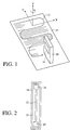
- Fig. 1 is a perspective view of a hand-held scanning device following a meandering path on an original.
- Fig. 2 is a bottom view of imaging and navigation sensors of the scanning device of Fig. 1.
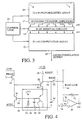
- Fig. 3 is a block diagram of a photoreceiver array and processing circuitry in accordance with the invention.
- Fig. 4 is a photoelement circuit connected to a transfer amplifier in accordance with the invention.
- Fig. 5 is a schematic diagram of a photoelement pair in accordance with the invention.
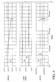
- Fig. 6 is a timing diagram for the circuit of Fig. 5.
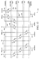
- Fig. 7 is a schematic diagram of the circuitry for operating the transfer amplifier of Fig. 4.
- Fig. 8 is a schematic diagram of a circuit for determining offset adjustment for the transfer amplifier of Fig. 7.
- Fig. 9 is a schematic diagram of the transfer amplifier of Fig. 4.
- Fig. 10 is a block diagram of an array of photoelements and transfer amplifiers in accordance with the invention.
- Fig. 11 is a block diagram of an array of switching networks and DC removal amplifiers to receive and process outputs from the transfer amplifiers of Fig. 10 in accordance with the invention.
- Fig. 12 is a schematic diagram of circuitry for switching signals transmitted to a DC removal amplifier of Fig. 11.
- Fig. 13 is a schematic diagram of circuitry for configuring the switching circuitry of Fig. 12.
- Fig. 14 is a schematic diagram of a DC removal amplifier of Fig. 11.
- Fig. 15 is a table of the transfer characteristics of each of four modes of operation for the DC removal amplifier of Fig. 14, as achieved by means of the configuration circuitry of Fig. 13.
- Fig. 16 is a schematic diagram of a circuit in which a photoreceiver output is delayed along only one of two parallel lines, so as to establish a signal relationship for subsequent two-dimensional DC removal.
- Fig. 17 is a schematic diagram of two-dimensional DC removal circuitry for connection to the circuit of Fig. 16.
- a portable, hand-held scanning device 10 is shown as having followed a meandering path 12 along an original 14.
- the original may be a piece of paper, but the invention may be used with other imaging-bearing substrates.
- the positions of inherent structural features, such as paper fibers may be tracked and the resulting positional information may be used to rectify image data.
- the invention may be used in other applications.
- the scanning device 10 is preferably self-contained and battery operated. However, the device may include a connection to an external source of power or to data ports of computers or networks.
- the scanning device includes an image display 16. The display may provide almost immediate viewing of a captured image. The display is not critical.
- the scanning device 10 allows three degrees of freedom, with two being in translation and one in rotation.
- the first degree is the side-to-side movement (X axis movement) along the original 14.
- the second degree of freedom is movement upwardly and downwardly along the original (Y axis movement).
- the third degree of freedom is the ability to operate the device with rotational misalignment of a linear array of image sensor elements relative to the edge of the original 14 ( ⁇ -misalignment as a result of Z axis movement). That is, it is not necessary to maintain the linear array of imaging elements perpendicular to the direction of device translation.
- the bottom side 18 of the scanning device 10 includes a pivoting member 20 that aids in maintaining proper contact between the original 14 and an imaging sensor 22.
- Navigation sensors 24 and 26 are located at the opposed ends of the imaging sensor. Because the navigation sensors are mounted on the pivoting member, the navigation sensors are in a fixed location relative to the imaging sensor.
- the imaging sensor 22 is preferably a contact image device, but for applications in which compactness is less of a concern or a smaller image is desired, sensors employing projection optics may be employed, with magnification less than unity.
- Contact imaging devices typically employ lenses sold under the trademark SELFOC, which is a federally-registered mark of Nippon Sheet Glass Company Limited. Less conventionally, contact imaging can be obtained using interleaved array elements of sources and proximal sensors, without any imaging lenses. Conventional imaging sensors for scanning applications may be used.
- the imaging sensor may be part of a unit that also includes an illumination source, illumination optics, and image transfer optics.
- the meandering path 12 is shown as having four and a fraction swaths, i.e., side-to-side passes across the original 14.
- a useful imaging sensor 22 for most applications has a length within the range of 25 mm and 100 mm.
- the swaths should include regions of overlap, so that a stitching process may be used to produce a faithful representation of the scanned original.
- the scanning device 10 includes at least one navigation sensor 24 or 26.
- the device includes a pair of navigation sensors, with the sensors being at opposite ends of the imaging sensor 22. While one-dimensional arrays of photoelements that are mounted orthogonally to each other may be used, the much preferred embodiment is one in which each navigation sensor is a two-dimensional array of elements.
- the navigation sensors 24 and 26 are used to track movement of the scanning device 10 relative to the original.
- Each navigation sensor is an array of photoelements that is formed on an integrated circuit substrate that includes readout and signal processing circuitry.
- the position accuracy necessary over the range of a pixel distance of 40 ⁇ m is 2.0 ⁇ m.
- the very high positional accuracy requires individual photoelements that are no larger than tens of microns in length in order to acquire sufficiently differing signals from element to element.
- the pixel size desired on the paper original 14 is 40 ⁇ m and a magnification of 1.5 is achieved by the imaging optics, so that the photoreceptor elements of the navigation sensors 24 and 26 are 60 ⁇ m ⁇ 60 ⁇ m. A greater optical magnification would enable larger pixels to be used.
- Each navigation sensor may be an array having sixty-four columns and thirty-two rows. However, none of these numbers is critical to the invention.
- the desired signal is the difference in reflectivity from pixel to pixel, as caused by variations along the surface of the original 14.
- the reflectivity may vary by only approximately six percent of the basic reflectivity of the white paper. Consequently, the circuitry to be described below must be designed to minimize noise and to ensure voltage stability.
- Fig. 3 is a block diagram of circuitry to be formed in a single integrated circuit chip.
- the chip is an analog signal processing chip designed to acquire and process two-dimensional images, providing cross-correlation information to an external controller, not shown.
- the controller uses the image cross-correlation values to derive X-Y position information.
- the X-Y position information is then used to accurately reconstruct a linear image from the image data acquired using imaging sensor 22 in Fig. 2.
- the navigation sensor 24 is an array having thirty-two rows and sixty-eight columns of photoelements.
- An array of sixty-eight column transfer amplifiers 17 transfers signals in a row-to-row fashion from the navigation sensor 24 to an array of sixty-four DC removal circuits 19.
- it is difficult to illuminate a target area with perfectly consistent light intensity across the entire area to be imaged.
- the ability to provide uniform illumination is often proportional to the cost of the optics and the light source.
- some variations in sensitivity will occur as a result of limitations of integrated circuit processing technology.
- a computational array 21 receives data from the DC removal circuits 19 and performs local difference computations on the data before transferring a cross-correlation output 23 to the off-chip controller. Also shown in Fig. 3 is a source 25 of control logic for the various components of the chip.
- Fig. 4 is a schematic diagram of a photoelement circuit.
- Fig. 5 is a more detailed circuit diagram of a photoelement pair.
- Incoming light is converted into a current that is integrated during a sample period. The stored value is periodically read out, so that it is available for a next step in a processing sequence.
- a reset switch 28 in Fig. 4 is turned “on” momentarily to reset an integration capacitor 30 to 3.25 volts.
- the reset switch 28 is a p-channel transistor that is turned “on” by applying a logic low to the gate of the transistor via a first reset line 32.
- Photocurrent that is generated by means of a photodiode 34 is amplified by a PNP transistor 36.
- the amplified photocurrent charges the integration capacitor 30 downwardly toward a level of 1.75 volts via a transistor 52.
- a read switch 42 is turned “on” to output the stored value along a read line 44 to a transfer amplifier 46.
- the read switch is an n-channel transistor that is controlled by a read control line 48.
- the photodiode 34 of the photoelement 40 generates a current in response to reception of light photons.
- the photodiode is connected to the base of the PNP transistor 36.
- the photodiode may be the base/collector portion of the transistor, so that the transistor is a phototransistor.
- the reverse bias diode capacitance 38 is a parasitic capacitance that may be 0.16 pF.
- the optical power on the photodiode was determined to be 1.1 nW. This causes a current of 0.6 nA in the diode current source. Because of the low current level, amplification is needed to ensure that the optical variation signal, which is only approximately six percent of the base photocurrent for applications in which surface texture is the image of interest, will create sufficient voltage differences to be distinguished from noise.
- the PNP transistor 36 of the photoelement 40 amplifies the photocurrent.
- the amplification provided by the transistor allows use of an integration capacitor 30 that facilitates reproducibility from photoelement to photoelement.
- the low current from the photodiode 34 would require a very small capacitor, e.g., 10 fF, as an integrator in order to get a 2 volt swing. Because of the parasitics, this would be difficult to reproduce on an element-to-element basis.
- Changing the photoelement layout from a diode to a substrate PNP device is a convenient way of providing current amplification.
- a beta value of 18 increases the output emitter current to 11.4 nA.
- an integration capacitor of 0.20 pF can be used. This facilitates reproducibility, but is not so large as to require excessive area.
- a concern with the circuit of Fig. 4 is that a direct beta dependency is introduced into the output current determination and, therefore, the integration capacitor voltage.
- testing has shown that matching of the devices from unit to unit is good, so that the effects of the beta dependency should be minor.
- a servo circuit is formed by three MOS transistors 50, 52 and 54.
- the three MOS transistors form an amplifier with a common gate stage 52 for the output of the phototransistor 36.
- the photodiode reverse voltage i.e., the transistor base voltage
- the photocurrent would be at least partially consumed in charging and discharging the diode capacitance 38 or the transistor base-collector capacitance, rather than providing current to be amplified by the substrate PNP transistor 36.
- the transistor base voltage at the node 56 is kept at a substantially fixed level by the three MOS transistors 50, 52 and 54. While not critical to achieving the desired operation, in the embodiment of Figs. 4 and 5 the substantially fixed voltage level is approximately equal to the NMOS threshold level above AVSS at the collector node 58.
- the three MOS transistors operate as a negative feedback loop by means of transistor 52 operating as a source follower to the emitter node 62 of the PNP transistor.
- the base voltage is controlled by the emitter voltage of the transistor. This is possible because the base voltage, i.e. the photodiode output at capacitor 30, has a very high impedance level.
- Transistor 52 acts as a common gate stage that has an added advantage of providing additional isolation of the emitter node 62 and the base node 56 of the transistor from the voltage swing of a PHTO1 node 64.
- the output voltage at the PHTO1 node 64 is held at 3.25 volts, i.e. VBB1, by the reset switching transistor 28. With the switching transistor electrically “on, " the CGN1 node 66 is held at approximately 2.6 volts and the emitter node 62 is held at approximately 1.4 volts. The base voltage at node 56 is near 1.0 volts.
- a photocurrent of approximately 0.6 nA flows from the base of the transistor 36 to the collector node 58, which is connected to AVSS.
- the reset signal at the first reset line 32 i.e. RST1B
- the output at the PHTO1 node 64 ramps downwardly in a linear manner as the current of the phototransistor 36 emitter is pulled from a capacitive structure formed by the gate-to-channel capacitance of a first n-channel transistor 68 in parallel with a second n-channel transistor 70.
- the transistors 68 and 70 of Fig. 5 are represented by the integration capacitor 30 in Fig. 4.
- the range of voltage of interest is from 3.25 volts to 1.75 volts. Consequently, the gates of the first and second n-channel transistors 68 and 70 are kept sufficiently high that the gate-to-channel capacitance of the devices is above the threshold level of the devices.
- the voltages at the emitter node 62 and the base node 56 remain stabilized by the negative feedback loop described above.
- the voltage at the base node stays within a range of approximately 2 mV.
- read switch 42 is turned “on” with a positive going gate pulse to transistor 42 by means of the read control line 48.
- the positive gate pulse lasts for approximately 200 ns.
- the operation of the transfer amplifier 46 pulls the PHTO1 node 64 down to 1.75 volts. This accomplishes the transfer of the signal from the integration capacitor 30 of Fig. 4 to the capacitor 72 in the transfer amplifier.
- the read control line 48 is caused to return to a logic low and the first reset line 32 is also caused to go low. This turns the reset switch 28 "on,” pulling the PHTO1 node 64 back up to 3.25 volts.
- a particular column transfer amplifier 46 will be described with reference to Fig. 4.
- the read line 44 is shunted to the second input 74 of the amplifier. That is, the two inputs are held at 1.75 volts.
- the output line 108 is connected to a second source of a fixed voltage. While not critical, the voltage at the output line 108 may be 3.25 volts.
- the integration capacitor 30 is also connected to 3.25 volts by means of the reset switch 28.
- the charge across the integration capacitor 30 will vary depending upon the photocurrent generated at the photoelement 40.
- the first input line 76 and the output line 108 of the transfer amplifier are disconnected from the fixed voltage sources of 1.75 volts and 3.25 volts, respectively.
- a positive perturbation is received at the first input line of the transfer amplifier.
- the output of the amplifier will go negative, pulling charge through the transfer capacitor 72 from the read line 44, bringing the voltage value back to 1.75 volts. This is caused by the gain of the amplifier.
- the operation of the computational array 21 of Fig. 3 is a correlation operation. If the initial part of the correlation operation is considered, the difference between signals of two nearest-neighbor photoelements is subtracted. Accurate interpretation of the data requires that the input signals to the computational array are strongly dependent upon the differences in optical illumination received at the various photoelements of the photoreceiver array 24. Consequently, the mismatch of devices resulting from manufacturing differences of devices will cause inaccuracies. Moreover, the integration time for the photoelements is 40 ⁇ s, providing a cycle time for reading out the entire array in the order of 50 ⁇ s. Since CMOS circuitry is preferred in order to achieve low power operation with high circuit density, 1/f noise is also a concern.
- the column transfer amplifier 46 is shown as having the first and second inputs 74 and 76 selectively shunted together by four transistor devices 78, 80, 82 and 84. Two of the transistors operate as switches. while the other two provide a degree of charge injection compensation. The switching of the transistor devices is controlled by a signal at a TRNRST line 86. When the signal on line 86 is high, inputs 74 and 76 are both connected to a source of a fixed voltage via the VBB3 line 88. In the example above, the VBB3 voltage is 1.75 volts. Inverters 110 and 112 provide the proper signal levels to the transistor devices 78-84.
- the signal on line 86 places the transfer amplifier in a reset mode.
- the transfer reset signal connects the inputs 74 and 76 together and simultaneously connects the output line 108 to a source of VBB2, via line 114.
- a second bank of four transistor devices 116 is controlled by the transfer reset signal on TRNRST line 86 in order to connect or disconnect the output line 108 to the source of VBB2.
- the VBB2 voltage is 3.25 volts. The selection of the input and output voltages ensures that the output voltage is centered approximately in the mid range of the operating voltage supply for subsequent stages.
- two of the devices are provided in order to achieve charge injection compensation.
- a third bank 118 of four transistor devices is included in order to selectively connect the output line 108 of the transfer amplifier 46 to a read feedback line 120.
- the third bank 118 and the read feedback line 120 form a portion of an offset adjustment loop. Again, two of the transistors in the bank are present solely for the purpose of charge injection compensation.
- a number of gates 122, 124, 126 and 128 and a clock device 130 are connected to provide proper operation of the second and third banks 116 and 118.
- Each of these devices operates in a conventional manner and may be readily replaced by other conventional circuitry, as will be understood by persons skilled in the art.
- Fig. 8 shows an offset adjustment amplifier 136 having a first node 138 connected to the VBB2 line 114 and having a second node 140 connected to the read feedback line 120.
- the offset adjustment amplifier 136 is common to all of the column transfer amplifiers 17 of the photoreceiver array 24 of Fig. 3. However, the second node 140 in Fig. 8 is connected to only one transfer amplifier at any given time. In fact, when the sixty-eight column transfer amplifiers are simultaneously in a readout mode, the second node 140 will be electrically isolated from receiving any signals from the transfer amplifiers.
- the voltage state at the read feedback line 120 is compared to the fixed voltage at the VBB2 line 114.
- the voltage states at nodes 138 and 140 will be identical, so that the voltage at output node 142 and at OFA line 144 will be at the nominal output bias level.
- variations in device fabrication and other performance mechanisms will generate offsets.
- the voltage states at nodes 138 and 140 will be different, producing an offset signal that is conducted to the circuitry block 132 via OFA line 144.
- line 144 is connected to the column transfer amplifier 46 to provide offset compensation of the transfer amplifier.
- the OFA line 144 is connected to the transfer amplifier 46 at an offset correction port 146, as shown in Fig. 7.
- Fig. 9 the internal circuitry of the transfer amplifier 46 is shown. Part of the circuitry of Fig. 9 is conventional and is readily understood by persons skilled in the art. Such conventional circuitry will not be explained herein. However, added to the conventional circuitry is an offset sample-and-hold circuit 148 that is accessed by the offset correction port 146 of the transfer amplifier. At the end of a reset operation in which the particular transfer amplifier is connected to the offset adjustment amplifier 136 of Fig. 8, the sample-and-hold circuit is refreshed.
- a signal received at a refresh port 150 of the transfer amplifier properly biases a fourth bank of transistor devices 152 for connecting the offset correction port 146 to OFAM line 154.
- the OFAM line 154 leads to a pair of transistors that combine to operate as a storage capacitor for the offset adjustment signal.
- a third transistor 160 is biased by the offset correction signal to provide offset compensation to the conventional circuitry of the transfer amplifier.
- the offset correction is achieved by forming a loop that originates at the output line 108 of the transfer amplifier 46 and continues to the offset correction port 146 of the transfer amplifier.
- VBB3 e.g. 1.75 volts
- VBB2 e.g. 3.25 volts
- the offset control operation is initiated by connecting the output line 108 to the read feedback line 120 by means of the third bank 118 of transistor devices.
- the voltage state at the read feedback line 120 will be equal to VBB2.
- the offset adjustment amplifier 136 compares the voltage at the read feedback line 120 to the anticipated voltage state, i.e. the VBB2 voltage.
- the amplifier 136 is a differential cell having an output node 142 connected to the offset adjustment line 144.
- This offset adjustment line completes the loop by connecting to the offset correction port 146 of the transfer amplifier 46, as shown in Figs. 8 and 9.
- the fourth bank 152 of transistor devices allows the signal at the offset correction port 146 to be stored by means of transistors 156 and 158. The stored charge provides offset correction to the transfer amplifier circuitry until the next refresh interval.
- each column transfer amplifier 46 is sequentially connected to the photoelements in a particular row of photoelements. In one embodiment, there are sixty-eight columns and thirty-two rows of photoelements.
- Fig. 10 illustrates five of the columns 162, 164, 166, 168 and 170, with each column being selectively connected to a different transfer amplifier 46, 172, 174, 176 and 178.
- the photoelement 40 of Fig. 4 is shown as being paired with a second photoelement 102 from the same column. Consequently, each photoelement is connected to the same read line 44 by means of turning "on" a read switch 42 and 101.
- Read control lines 48 and 90 provide individual control of the read switches, so that no two photoelements will be connected to the transfer amplifier simultaneously.
- reset devices 28 and 92 that are connected to separate reset lines 32 and 94 and to the separate PHTO nodes 64 and 96.
- the second photoelement includes its own common gate arrangement provided by MOS transistors 98, 99 and 100 that operate in the same manner as the MOS transistors 50, 52 and 54 of the first photoelement 40.
- the second photoelement includes storage-capacitive transistors 104 and 106 that operate as the integration capacitor for the second photoelement.
- the integration time for the photoelements 40 and 102 in each column 162-170 is approximately 40 ⁇ s.
- the read switch 42 of the first row of photoelements 40 is closed, so that each transfer capacitor 72 of the various transfer amplifiers 46, 172, 174, 176 and 178 receives a charge corresponding to the light energy that strikes the photoelement 40 in the first row.
- the received charge is transferred to subsequent processing circuitry via output lines 108, 180, 182, 184 and 186.
- the readout time of a single row is estimated to be between 200 ns and 300 ns.
- the read switches 42 are opened and the read switches 101 of the second row of photoelements 102 are closed. The process is repeated until each row of photoelements is read.
- the offset adjustment operation described above requires no more than 4 ⁇ s. Therefore, at least eight transfer amplifiers 46 and 172-178 can be connected to the offset adjustment amplifier 136 of Fig. 8 in a sequential manner during each 40 ⁇ s integration interval in which the transfer amplifiers are idle between transfer operations.
- the sample-and-hold circuit 148 of each transfer amplifier is designed to ensure that there is no significant voltage droop at the storage capacitance provided by transistors 156 and 158. Thus, reset can occur without a time sacrifice with respect to transferring photoelement signals.
- a concern in the processing of signals from the navigation array 24 of photoelements through the computational array 21 of Fig. 3 involves potential corruption of the processing as a result of a characteristic that is common within a neighborhood of photoelements.
- a scanner may have a source for illuminating the substrate as the scanner is moved relative to an original. It is difficult to illuminate an entire viewing region without variations in illumination. Signal processing may be adversely affected by such variations.
- the DC removal circuits 19 of Fig. 3 have the basic function of removing low spatial frequency variations within the neighborhood of photoelements. As noted above, the DC removal circuits may also have a low-pass characteristic that may be set to remove spatial frequency components at high frequencies. Thus, the DC removal circuits can have a band pass characteristic.
- the DC removal circuits transform the original image into an image of local differences. The local differences approach results in the original image being destroyed, but for applications such as the determination of scanner movement relative to an original, this is not a concern. The removal of low spatial frequencies maintains the integrity of correlation signals. Moreover, the local differences approach has the additional advantage of reducing the dynamic range requirements of the computation array 21, which actually calculates the image cross-correlations.
- the removal of low spatial frequencies renders the navigation operation less susceptible to such things as the navigation sensor being positioned so that one major region of the array views paper fibers of a shaded region of a scanned original, while the paper fibers viewed by a second portion of the array are outside of the shaded region.
- each switching network gates its inputs through a series of switches controlled by digital control inputs from the control logic 25 of Fig. 3.
- the outputs of each switching network 198-206 are connected to an associated DC removal amplifier 208, 210 and 212.
- the DC removal circuits may be in any one of a number of modes, including a test mode and a DC removal disabled mode.
- the DC removal amplifier 210 of Fig. 11 an example of four possible modes of operation of the DC removal amplifier 210 of Fig. 11 are characterized.
- NODCR no DC removal
- the output 236 of the amplifier 210 is the same as the input INP, which is connected directly to the photoreceiver output line 192 by the switching network 202.
- TST test
- the output signal of the DC removal amplifier is dependent upon three known test outputs: TC, TL and TR.
- the switching network 202 is not connected to the nearest neighbor photoreceivers, a wider sampling for removing low frequency information is acquired.
- the "primary input" in the F1 and F2 modes is the PHR(i) output, and local differencing is achieved by the subtraction of secondary inputs from PHR(i+2) and PHR(i-2).
- the switching network 202 receives inputs from photoreceiver outputs 188 and 196, which are the photoreceivers removed by two from the photoreceiver of interest.
- the photoreceiver outputs are received via the transfer amplifiers described previously.
- DCRCM DC removal common mode
- the switching network is configured by setting a binary input pair CFIG1 222 and CFIG0 224 to one of four possible combinations.
- a calibration signal may be received at CAL line 226.
- the CAL signal is used to provide a condition in which only the INP(i) line 228 conducts a signal from the switching network 202 to the DC removal amplifier 210.
- the CAL signal disconnects the DIN outputs 230, 232 and 234 during an offset correction operation that is separate from the offset control operation of the transfer amplifiers.
- the circuitry of Figs. 11-13 can be configured on one of four ways by controlling the configuration signals at lines 222 and 224.
- a first mode DC removal is disabled.
- the DIN signals along outputs 230, 232 and 234 are not utilized in this mode, since gates 242 and 252 in Fig. 13 do not provide the required DC removal enable signals at lines 244-250, 256 and 258.
- the configuration signals at lines 222 and 224 define a test mode in which gate 242 provides enabling signals at lines 244 and 246.
- the DCRCM common mode input 220 is passed through the switching network 202 to INP(i) line 228.
- Test inputs TL 214, TR 216 and TC 218 are passed through to outputs 234, 232 and 230, respectively.
- the test inputs are known signals, allowing complete characterization of the DC removal amplifier 210.
- a third configuration of the switching network 202 is referred to as the DC removal function 1 mode.
- This third mode is enabled by providing a logic high at line 250 and a logic low at line 248 by means of gate 252.
- the fourth configuration is referred to as a DC removal function 2 mode.
- the F2 mode connects the DINM1(i) output 232 to the PHR(i+2) line 196.
- Gate 254 triggers the proper signals along lines 256 and 258 for enabling the F2 mode.
- the DC removal amplifier 210 is shown in Fig. 14.
- the amplifier includes a first differential cell Ay 260 and a second differential cell Ax 262.
- the INP(i) output 228 is received at the second differential cell, while the other three outputs 230, 232 and 234 from Fig. 12 are received at the first differential cell.
- the second differential cell 262 includes a differential pair of transistors 264 and 266.
- Transistors 268 and 270 provide a current mirror load for transistors 264 and 266.
- a folded cascode output stage is formed by four serially connected transistors 272. 274. 276 and 278.
- transistors 280 and 282 are biased by voltages NCON4 and PCON4 to act as constant current sources. These two voltages. as well as bias voltages VBP and VBN, are generated and provided by constant voltage sources.
- the DC removal amplifier 210 includes offset correction circuitry.
- Transistors 284 acts as a switch to achieve unity gain feedback.
- Offset correction transistors 286, 288, 290 and 292 are biased in the triode region to introduce offset correction into the amplifier.
- Equation (3) Transconductance gm x is modulated by a bank 300 of eight transistors.
- the transistors in the bank are biased in the triode region by a voltage GAINADJ to act as gain degeneration resistors to the differential pair of transistors 264 and 266.
- the other four transistors in the bank 300 are used as switches to selectively shunt the gain degeneration resistive transistors and are under the control of the G1 and G2 digital gain control inputs.
- the G1 and G2 voltages are set by the control logic 25 shown in Fig. 3.
- the four resistive transistors 302, 304, 306 and 308 may be referred to as r 302 , r 306 , r 306 and r 308 , respectively.
- the values G1 ⁇ and G2 ⁇ are the boolean complements of the digital control inputs G1 and G2 and have values of 0 or 1.
- the values of the degeneration resistors r 302 -r 308 are modulated by varying the control voltage input GAINADJ signal at line 310.
- switching network 202 of Figs. 12 and 13 may be used to set the DC removal amplifier 210 in any one of four modes.
- Fig. 15 is the table which summarizes the transfer characteristics of the circuitry in each of the four modes.
- the DC removal modes of F1 and F2 low spatial frequency components of the photoreceiver output 192 of Fig. 11 are removed in effect by subtracting from a signal of interest the average of the signals received by a DC removal amplifier 210 from two or more photoreceivers.
- the signal of interest is the PHR(i) signal from line 192. This signal is received at the DINP(i) line 230 in Fig. 14.
- PHR(i) is shown as being multiplied by two in the equation of the F1 mode.
- the signal from PHR(i-2) is switched to both the DINM1(i) line 232 and the DINM0(i) line 234, so that PHR(i-2) is also multiplied by two.
- the difference value is multiplied by gm y /gm x , which is subtracted from the DCRCM value.
- the DCRCM value is selected to establish a positive mid range voltage value for subsequent processing of the analog signal at WDATA(i) line 236.
- the signals at the INP(i) line 228, the DINP(i) line 230 and DINM0(i) line 234 remain the same, but the DINM1(i) line 232 is switched from connection with the PHR(i-2) output line 188 to the PHR(i+2) line 196.
- the filtering of common components occurs, but the commonality is with reference to three photoreceivers, rather than two.
- Photoreceiver PHR(i) controls transistors 314 and 316.
- Photoreceiver PHR(i-2) controls transistor 318, while photoreceiver PHR(i+2) controls transistor 320.
- the number of transistors controlled by each photoreceiver, or the areas of such transistors, can be varied to vary the weighting of the different photoreceivers.
- Figs. 16 and 17 provide a modification of the F2 mode.
- the signal from a photoreceiver is conducted without delay to the line 192.
- the signal along 192 is in real time (t).
- a pair of delay circuits 290 and 292 is connected in series along a second line 294.
- the signal at the line 294 is the photoreceiver output with a delay of 2 ⁇ .
- the delay circuits 290 and 292 along the second line 294 allow two-dimensional DC removal. That is, a secondary input for DC removal may be from a different row within the same column as the source of the primary input.
- the circuit of Fig. 17 is used to implement the F2 mode of operation. Common lines in Figs. 12 and 17 are identified by identical reference numerals.
- the circuit of Fig. 17 remains the same with respect to the primary input at line 192 and one of the secondary inputs at line 188.
- the secondary input at line 294 is from the same transfer amplifier as the primary input at line 192.
- the input is from the same column, but the delay of 2 ⁇ results in the secondary input being from a different row.
- the delay ⁇ is equal to the sampling time of the transfer amplifiers.
- delay circuits 290 and 292 in Fig. 16 are not critical to the operation of the two-dimensional DC removal function.
- the appropriate secondary inputs may be provided by sample-and-hold circuits that operate in a round robin fashion.
- Figs. 12-14 and Figs. 16 and 17 efficiently overcome the adverse effects of variations in illumination of a substrate that is viewed by a photoreceiver array. Moreover, in the use of the invention in providing navigation information, as set forth above, the navigation operation is less affected by such things as one portion of a navigation array viewing paper fibers of a shaded region of a scanned original, while the paper fibers viewed by a second portion of the array are outside of the shaded region of the original.
- the DC removal amplifier 210 of Fig. 14 includes offset correction to reduce voltage offsets, such as those generated by manufacturing-induced variations in device parameters.
- Transistors 322, 324, 326, 328, 330 and 332 are employed to implement offset correction.
- transistor 322 is switched “on” with the CAL input signal at line 226, thereby connecting the DC removal amplifier output WDATA(i) to an OFST_CTRL node 334.
- the negative feedback as shown by line 298 in Fig. 11 at the second differential cell 262 is disconnected by turning "off” transistor 284.
- the differential inputs to the cells 260 and 262 are shorted out by the shunt switch transistors 328, 330 and 332.
- the DC removal amplifier 210 amplifies the input offset. Offset correction transistors 286, 288, 290 and 292 are biased in the triode region. If the voltage at OFST_CTRL node 334 is not equal to bias voltage VBP, current mirrors provided by transistors 268 and 270 and transistors 336 and 338 will be unbalanced and will create an additional voltage at the WDATA(i) output 236.
- a o1 being the open loop gain of the amplifier 210 from the conventional inputs
- the amplifier is designated to have the following relationship between the OFST_CTRL node and the output 236: WDATA(i) ⁇ A 01 100 (vbs - OFST_CTRL)
- the amplifier output connected to the OFST_CTRL node via transistor 322
- a new negative feedback path is introduced. Since the gain from the OFST_CTRL node to the amplifier output is approximately 100 times less than the gain from conventional input to output, the temporary negative feedback path created by means of transistor 322 causes a signal equal to 100 times the input offset to be developed between OFST_CTRL and the bias voltage VBP.
- the CAL input is brought to logic low, so that the OFST_CTRL node 334 is disconnected from the WDATA(i) output 236.
- Transistor 324 is used as a capacitor approximately equal to 300 fF.
- the offset correction signal generated during the correction cycle is stored as charge at the gate of the transistor 324. If desired, offset correction may be disabled by driving the gate of transistor 326 low via line 340, thereby shunting the OFST_CTRL node 334 to the bias input VBP.
Abstract
Description
- The present invention relates generally to signal transfer circuitry and more particularly to circuitry for transferring individual signals from an array of photoreceivers to computational circuitry.
- An accurate determination of the path of a device across a surface is important in a variety of applications. For example, if a faithful representation of an image of a scanned original is to be acquired, there must be accurate information as to the travel of the scanning device along the original. Typically, the captured image provided by a scanner is a pixel data array that is stored in memory in a digital format. A distortion-free image requires a faithful mapping of the original image to the pixel data array.
- U.S. Pat. No. 5,149,980 to Ertel et al., which is assigned to the assignee of the present invention, describes use of a cross-correlation function to determine the relative movement between an original and an array of photoelements in a given direction. The patent notes that the one-dimensional approach can be extended to determine the vector of two-dimensional relative movement between the original and the array, so as to track translation, rotation and scaling in a two-dimensional plane.
- The patent to Ertel et al. describes use of an optical sensor array to collect some form of "signature" of an original. The signature may be provided by illuminating and imaging the surface texture or other optical characteristics of the original. The light intensity will vary on a pixel-by-pixel basis with variations in surface texture. By cross-correlating images of the surface of the original, relative movement between the array and the original can be ascertained.
- A critical element of the design of a system such as the one described by Ertel et al. is the circuitry which maintains the signal-to-noise ratio of each photoelement at a sufficiently high level to reliably determine the signature of the original. If the signal is the difference in reflectivity from pixel to pixel as a result of slight variations in paper texture of a white paper, the variations in reflectivity may be approximately six percent. If the sample rate objectives and the amount of possible subsequent signal averaging are considered, then noise terms in the signal must be less than the six percent paper reflectivity variation signal if useful information is to be obtained.
- Thus, noise is one concern in the processing of signals from photoelements in a photoreceiver array. Another concern is manufacturing-induced variations in the performance of processing circuitry. Operations that rely upon computations of the differences in reflectivity from one pixel to another pixel are susceptible to error if electrically parallel transfer circuits vary in performance. In the ideal, there are no pixel-to-pixel signal differences due to variations in signal transfer circuit performance, so that differences between pixel signals are solely attributable to differences in light reception at the photoelements. However, circuit devices vary in performance, even when the devices are formed by the same fabrication process.
- Yet another concern involves reliably obtaining useful information regarding an imaged surface when there are image-affecting considerations that are consistent among pixels in one neighborhood of pixels, but different among pixel neighborhoods. For example, illumination optics may create consistent neighborhood-to-neighborhood variations in the illumination of the surface to be imaged. Non-uniform illumination will cause artifacts. Another example of a consistent localized pattern is one in which a portion of the photoelement array is directed at a surface area having a dark background, while the remainder of the photoelements are directed at an unshaded area of the surface.
- What is needed is transfer circuitry for connection to a photoreceiver arrangement, with the circuitry having a reduced susceptibility to errors caused by manufacturing-induced variations of devices and by multiple-pixel patterns of photoelement signal generation and/or processing.
- Circuitry and a method for transferring signals from a photoelement array to computational circuits include parallel transfer amplifiers that receive periodic offset correction to reduce the susceptibility of signal processing to differences in performance among the transfer amplifiers. In another embodiment, the circuitry for transferring signals includes spatial frequency band filtering amplifiers to suppress the effects of such artifacts as multi-photoelement patterns of light reception at the photoelement array.
- In the following disclosure, the term "DC removal" will be used as a shorthand term to denote spatial frequency band filtering. It is to be understood that the term "DC removal," as used herein, encompasses not only the removal of DC spatial components, but also the removal of spatial frequency components at either or both low and high frequencies.
- At the transfer amplifier level, when in a readout mode, each transfer amplifier has a first input that is connected to receive a signal indicative of light received at a photoelement. The photoelements in the array may be arranged in columns and rows, with the photoelements in a particular column being sequentially connected to the first input of a particular transfer amplifier, but this is not critical. Each transfer amplifier has a second input connected to a source of a reference voltage (e.g., 1.75 volts). The transfer amplifiers operate as differential circuits, so that an output is responsive to the difference between the voltage states at the first and second inputs. However, during a reset interval between readout intervals, both of the first and second inputs are connected to the source of the reference voltage. Moreover, the output of a transfer amplifier is momentarily connected to a source of a reset voltage (e.g., 3.25 volts). An offset reduction circuit is provided to generate an offset adjustment signal in response to detecting a voltage difference between the reset voltage and the voltage state at the output after the output has been disconnected from the source of the reset voltage. In this manner, the adjustment signal may be applied to the transfer amplifier of interest to reduce or eliminate any difference in performance between the transfer amplifier and other transfer amplifiers.
- An advantage of the offset-adjusted transfer amplifier embodiment is that the influence of device-to-device variations and 1/f noise is taken into account. The cycle time for reading out an entire array may be in the order of 50 µs. Since CMOS circuitry is preferred, in order to achieve low power operation with a high circuit density, 1/f noise would potentially cause significant fluctuations in the outputs of the amplifiers, if such noise were not suppressed. Another advantage of the invention is that each transfer amplifier preferably includes a sample-and-hold arrangement to store the offset adjustment signal, so that each transfer amplifier only needs to be periodically refreshed. Thus, a single circuit for determining offset adjustment signals may be used for all of the transfer amplifiers. A timing sequence is provided to achieve periodic refreshes without lengthening intervals between photoelement signal readouts.
- Since each transfer amplifier includes the sample-and-hold arrangement, the transfer amplifiers have three modes of operation. In a readout mode, the second input is connected to the source of the reference voltage, while the first input is connected to a photoelement. As a result, a charge will be transferred to an operatively associated integration capacitor. The amplifier output voltage is in turn supplied to downstream processing circuitry. The internal sample-and-hold arrangement will provide offset correction. A second mode of operation is a passive reset mode. The reset is "passive" because the offset adjustment signal is not updated. The passive reset mode may be of poor quality until the first active offset adjustment operation has been executed. In the passive reset mode, the two inputs of the transfer amplifier are connected together and the output remains connected to the source of the reset voltage. The third mode of operation is the active reset mode. Like the passive reset mode, the two inputs of a transfer amplifier are connected to the source of the reference voltage. However, the output is only momentarily connected to the source of the reset voltage. Once disconnected, the output is connected to the offset adjustment circuit, which determines the appropriate offset adjustment signal to be stored by the sample-and-hold arrangement until the next active reset operation.
- Between the periodic updates of the offset adjustment signal, each transfer amplifier alternates between the readout mode and the passive reset mode. The 1/f offset drift components are sufficiently slow, so that an update after each eighth readout of the photoelement array is an adequate rate.
- As previously noted, the invention also includes DC removal amplifiers to suppress multi-photoelement light patterns and other artifacts. The DC removal amplifiers remove spatial frequency components at both low and high frequencies from the outputs of the transfer amplifiers. There may be a one-to-one correspondence of DC removal amplifiers to transfer amplifiers. Each DC removal amplifier includes a primary input that is connected to receive a signal of interest from a particular photoelement. Each DC removal amplifier also includes at least one secondary input connected to receive an output signal from a photoelement proximal to the particular photoelement. In effect, an averaging of the secondary inputs occurs and the resulting average value is subtracted from the primary input. The DC removal amplifiers, in addition to removing low spatial frequency components, also have an inherent low-pass characteristic at a frequency corresponding to twice the pixel spacing. Thus, the DC removal amplifiers inherently have a band-pass characteristic. The inherent low-pass element of the band-pass characteristic may be modified by multiplying the secondary inputs by different weighting factors prior to the averaging. The weighting factors can be positive or negative numbers.
- The DC removal amplifier may be formed of first and second differential cells, with the second differential cell having a negative feedback loop from its output to its input. The second differential cell may also have a DC input to establish a mid range voltage that facilitates downstream differential operations. While not critical to the invention, the DC removal amplifier may include offset correction and may include a switching network that enables a user to switch inputs to the DC removal amplifier or to set the operation of the amplifier in a test mode.
- The invention will be better understood by reference to the following description of exemplary embodiments thereof. In the accompanying drawings:
- Fig. 1 is a perspective view of a hand-held scanning device following a meandering path on an original.
- Fig. 2 is a bottom view of imaging and navigation sensors of the scanning device of Fig. 1.
- Fig. 3 is a block diagram of a photoreceiver array and processing circuitry in accordance with the invention.
- Fig. 4 is a photoelement circuit connected to a transfer amplifier in accordance with the invention.
- Fig. 5 is a schematic diagram of a photoelement pair in accordance with the invention.
- Fig. 6 is a timing diagram for the circuit of Fig. 5.
- Fig. 7 is a schematic diagram of the circuitry for operating the transfer amplifier of Fig. 4.
- Fig. 8 is a schematic diagram of a circuit for determining offset adjustment for the transfer amplifier of Fig. 7.
- Fig. 9 is a schematic diagram of the transfer amplifier of Fig. 4.
- Fig. 10 is a block diagram of an array of photoelements and transfer amplifiers in accordance with the invention.
- Fig. 11 is a block diagram of an array of switching networks and DC removal amplifiers to receive and process outputs from the transfer amplifiers of Fig. 10 in accordance with the invention.
- Fig. 12 is a schematic diagram of circuitry for switching signals transmitted to a DC removal amplifier of Fig. 11.
- Fig. 13 is a schematic diagram of circuitry for configuring the switching circuitry of Fig. 12.
- Fig. 14 is a schematic diagram of a DC removal amplifier of Fig. 11.
- Fig. 15 is a table of the transfer characteristics of each of four modes of operation for the DC removal amplifier of Fig. 14, as achieved by means of the configuration circuitry of Fig. 13.
- Fig. 16 is a schematic diagram of a circuit in which a photoreceiver output is delayed along only one of two parallel lines, so as to establish a signal relationship for subsequent two-dimensional DC removal.
- Fig. 17 is a schematic diagram of two-dimensional DC removal circuitry for connection to the circuit of Fig. 16.
- With reference to Fig. 1, a portable, hand-held
scanning device 10 is shown as having followed a meanderingpath 12 along an original 14. The original may be a piece of paper, but the invention may be used with other imaging-bearing substrates. In use of the hand-held scanning device, the positions of inherent structural features, such as paper fibers, may be tracked and the resulting positional information may be used to rectify image data. However, the invention may be used in other applications. - The
scanning device 10 is preferably self-contained and battery operated. However, the device may include a connection to an external source of power or to data ports of computers or networks. The scanning device includes animage display 16. The display may provide almost immediate viewing of a captured image. The display is not critical. - The
scanning device 10 allows three degrees of freedom, with two being in translation and one in rotation. The first degree is the side-to-side movement (X axis movement) along the original 14. The second degree of freedom is movement upwardly and downwardly along the original (Y axis movement). The third degree of freedom is the ability to operate the device with rotational misalignment of a linear array of image sensor elements relative to the edge of the original 14 (θ-misalignment as a result of Z axis movement). That is, it is not necessary to maintain the linear array of imaging elements perpendicular to the direction of device translation. - Referring now to Figs. 1 and 2, the
bottom side 18 of thescanning device 10 includes a pivotingmember 20 that aids in maintaining proper contact between the original 14 and animaging sensor 22.Navigation sensors - For reasons of physical compactness, the
imaging sensor 22 is preferably a contact image device, but for applications in which compactness is less of a concern or a smaller image is desired, sensors employing projection optics may be employed, with magnification less than unity. Contact imaging devices typically employ lenses sold under the trademark SELFOC, which is a federally-registered mark of Nippon Sheet Glass Company Limited. Less conventionally, contact imaging can be obtained using interleaved array elements of sources and proximal sensors, without any imaging lenses. Conventional imaging sensors for scanning applications may be used. The imaging sensor may be part of a unit that also includes an illumination source, illumination optics, and image transfer optics. - In Fig. 1, the meandering
path 12 is shown as having four and a fraction swaths, i.e., side-to-side passes across the original 14. Auseful imaging sensor 22 for most applications has a length within the range of 25 mm and 100 mm. The swaths should include regions of overlap, so that a stitching process may be used to produce a faithful representation of the scanned original. - The
scanning device 10 includes at least onenavigation sensor imaging sensor 22. While one-dimensional arrays of photoelements that are mounted orthogonally to each other may be used, the much preferred embodiment is one in which each navigation sensor is a two-dimensional array of elements. Thenavigation sensors scanning device 10 relative to the original. - Each navigation sensor is an array of photoelements that is formed on an integrated circuit substrate that includes readout and signal processing circuitry. The position accuracy necessary over the range of a pixel distance of 40 µm is 2.0 µm. The very high positional accuracy requires individual photoelements that are no larger than tens of microns in length in order to acquire sufficiently differing signals from element to element. In the preferred embodiment, the pixel size desired on the paper original 14 is 40 µm and a magnification of 1.5 is achieved by the imaging optics, so that the photoreceptor elements of the
navigation sensors - In the operation of the
navigation sensors - Fig. 3 is a block diagram of circuitry to be formed in a single integrated circuit chip. The chip is an analog signal processing chip designed to acquire and process two-dimensional images, providing cross-correlation information to an external controller, not shown. In the embodiment described above, the controller uses the image cross-correlation values to derive X-Y position information. The X-Y position information is then used to accurately reconstruct a linear image from the image data acquired using
imaging sensor 22 in Fig. 2. - In the embodiment of Fig. 3, the
navigation sensor 24 is an array having thirty-two rows and sixty-eight columns of photoelements. An array of sixty-eightcolumn transfer amplifiers 17 transfers signals in a row-to-row fashion from thenavigation sensor 24 to an array of sixty-fourDC removal circuits 19. In a cost-efficient image-capture system, it is difficult to illuminate a target area with perfectly consistent light intensity across the entire area to be imaged. The ability to provide uniform illumination is often proportional to the cost of the optics and the light source. Moreover, in the absence of cell-by-cell calibration of a conventional integrated light sensor, some variations in sensitivity will occur as a result of limitations of integrated circuit processing technology. In the navigation system for use with the analog signal processing chip of Fig. 3, it is required that cross-correlations be calculated between an incident image and an image captured previously at a different location relative to an imaging array. Any variations in illumination and photoelement sensitivity will degrade the correlation signal. Consequently, the spatialDC removal circuits 19 of Fig. 3 have been designed to maintain the integrity of the correlation signals, while keeping the cost of the system relatively low. Low spatial frequency changes in illumination and photoelement sensitivity which would otherwise corrupt the correlation signal are removed from the navigation image. In addition, the DC removal circuits also have an inherent low-pass characteristic. Acomputational array 21 receives data from theDC removal circuits 19 and performs local difference computations on the data before transferring across-correlation output 23 to the off-chip controller. Also shown in Fig. 3 is asource 25 of control logic for the various components of the chip. - Fig. 4 is a schematic diagram of a photoelement circuit. Fig. 5 is a more detailed circuit diagram of a photoelement pair. Incoming light is converted into a current that is integrated during a sample period. The stored value is periodically read out, so that it is available for a next step in a processing sequence. At the start of an integration cycle, a
reset switch 28 in Fig. 4 is turned "on" momentarily to reset anintegration capacitor 30 to 3.25 volts. As shown in Fig. 5, thereset switch 28 is a p-channel transistor that is turned "on" by applying a logic low to the gate of the transistor via afirst reset line 32. Photocurrent that is generated by means of aphotodiode 34 is amplified by aPNP transistor 36. The photodiode and the transistor, along with aparasitic capacitance 38, define aphotoelement 40. The amplified photocurrent charges theintegration capacitor 30 downwardly toward a level of 1.75 volts via atransistor 52. At the end of the sample period, aread switch 42 is turned "on" to output the stored value along a readline 44 to atransfer amplifier 46. As shown in Fig. 5, the read switch is an n-channel transistor that is controlled by aread control line 48. - The
photodiode 34 of thephotoelement 40 generates a current in response to reception of light photons. The photodiode is connected to the base of thePNP transistor 36. The photodiode may be the base/collector portion of the transistor, so that the transistor is a phototransistor. The reversebias diode capacitance 38 is a parasitic capacitance that may be 0.16 pF. In the embodiment described above, in which there is a 32 x 68 element array, the optical power on the photodiode was determined to be 1.1 nW. This causes a current of 0.6 nA in the diode current source. Because of the low current level, amplification is needed to ensure that the optical variation signal, which is only approximately six percent of the base photocurrent for applications in which surface texture is the image of interest, will create sufficient voltage differences to be distinguished from noise. - The
PNP transistor 36 of thephotoelement 40 amplifies the photocurrent. The amplification provided by the transistor allows use of anintegration capacitor 30 that facilitates reproducibility from photoelement to photoelement. In the absence of amplification, the low current from thephotodiode 34 would require a very small capacitor, e.g., 10 fF, as an integrator in order to get a 2 volt swing. Because of the parasitics, this would be difficult to reproduce on an element-to-element basis. Changing the photoelement layout from a diode to a substrate PNP device is a convenient way of providing current amplification. A beta value of 18 increases the output emitter current to 11.4 nA. Thus, an integration capacitor of 0.20 pF can be used. This facilitates reproducibility, but is not so large as to require excessive area. - A concern with the circuit of Fig. 4 is that a direct beta dependency is introduced into the output current determination and, therefore, the integration capacitor voltage. However, testing has shown that matching of the devices from unit to unit is good, so that the effects of the beta dependency should be minor.
- A servo circuit is formed by three
MOS transistors common gate stage 52 for the output of thephototransistor 36. To achieve proper transfer of the current generated in thephotoelement 40 to theintegration capacitor 30, the photodiode reverse voltage (i.e., the transistor base voltage) must be kept at a substantially constant level. If the voltage at thebase node 56 were to be allowed to shift, the photocurrent would be at least partially consumed in charging and discharging thediode capacitance 38 or the transistor base-collector capacitance, rather than providing current to be amplified by thesubstrate PNP transistor 36. - The transistor base voltage at the
node 56 is kept at a substantially fixed level by the threeMOS transistors collector node 58. The three MOS transistors operate as a negative feedback loop by means oftransistor 52 operating as a source follower to theemitter node 62 of the PNP transistor. Thus, the base voltage is controlled by the emitter voltage of the transistor. This is possible because the base voltage, i.e. the photodiode output atcapacitor 30, has a very high impedance level.Transistor 52 acts as a common gate stage that has an added advantage of providing additional isolation of theemitter node 62 and thebase node 56 of the transistor from the voltage swing of aPHTO1 node 64. - Referring now to Figs. 4, 5 and 6, for the reset period, the output voltage at the
PHTO1 node 64 is held at 3.25 volts, i.e. VBB1, by thereset switching transistor 28. With the switching transistor electrically "on, " theCGN1 node 66 is held at approximately 2.6 volts and theemitter node 62 is held at approximately 1.4 volts. The base voltage atnode 56 is near 1.0 volts. - When the light source that illuminates the medium of interest is turned "on," a photocurrent of approximately 0.6 nA flows from the base of the
transistor 36 to thecollector node 58, which is connected to AVSS. At 7.0 µs from the start of the timing sequence of Fig. 6, the reset signal at thefirst reset line 32, i.e. RST1B, is caused to go to logic high, thereby turning "off" thereset switch 28. As a result, the output at thePHTO1 node 64 ramps downwardly in a linear manner as the current of thephototransistor 36 emitter is pulled from a capacitive structure formed by the gate-to-channel capacitance of a first n-channel transistor 68 in parallel with a second n-channel transistor 70. Thetransistors integration capacitor 30 in Fig. 4. The range of voltage of interest is from 3.25 volts to 1.75 volts. Consequently, the gates of the first and second n-channel transistors - During the integration time in which the
reset switch 28 is "off, " the voltages at theemitter node 62 and thebase node 56 remain stabilized by the negative feedback loop described above. The voltage at the base node stays within a range of approximately 2 mV. - After approximately 20 microseconds of integration time, for this simulation exercise, read
switch 42 is turned "on" with a positive going gate pulse totransistor 42 by means of the readcontrol line 48. The positive gate pulse lasts for approximately 200 ns. The operation of thetransfer amplifier 46 pulls thePHTO1 node 64 down to 1.75 volts. This accomplishes the transfer of the signal from theintegration capacitor 30 of Fig. 4 to thecapacitor 72 in the transfer amplifier. At the conclusion of the transfer process, theread control line 48 is caused to return to a logic low and thefirst reset line 32 is also caused to go low. This turns thereset switch 28 "on," pulling thePHTO1 node 64 back up to 3.25 volts. - The basic operation of a particular
column transfer amplifier 46 will be described with reference to Fig. 4. When the transfer amplifier is not in a readout mode, the readline 44 is shunted to thesecond input 74 of the amplifier. That is, the two inputs are held at 1.75 volts. At the same time, theoutput line 108 is connected to a second source of a fixed voltage. While not critical, the voltage at theoutput line 108 may be 3.25 volts. Theintegration capacitor 30 is also connected to 3.25 volts by means of thereset switch 28. - Referring to Figs. 4 and 5, when the
reset switch 28 is opened, the charge across theintegration capacitor 30 will vary depending upon the photocurrent generated at thephotoelement 40. Following an integration period of approximately 40 µs, thefirst input line 76 and theoutput line 108 of the transfer amplifier are disconnected from the fixed voltage sources of 1.75 volts and 3.25 volts, respectively. Upon connection of theintegration capacitor 30 to thefirst input line 76 by turning theread switch 42 "on," a positive perturbation is received at the first input line of the transfer amplifier. The output of the amplifier will go negative, pulling charge through thetransfer capacitor 72 from the readline 44, bringing the voltage value back to 1.75 volts. This is caused by the gain of the amplifier. Since charge is conserved, the amount of charge required to bring theintegration capacitor 30 from its final integration value to the potential, i.e. 1.75 volts, of thesecond input line 74 is pulled from theintegration capacitor 30 onto thetransfer capacitor 72. The equation governing the operation of the integration and charge transfer is:
- out
- is the output voltage of the transfer amplifier at the end of the transfer operation,
- Vout
- is the starting voltage at the output line 108 (i.e., 3.25 volts),
- Vcap
- is the starting voltage for the integration capacitor (i.e., 3.25 volts),
- Iph
- is the photodiode current (i.e., 0.6 nA),
- β
- is the beta of the photo transistor 36 (i.e., 18).
- Tint
- is the integration time for the photoreceiver (i.e., 40 µs),
- Cint
- is the value of the integration capacitor (i.e., 0.2 pF),
- Vbott
- is the bias value at the
second input 74 of the transfer amplifier (i.e., 1.75 volts), and - Ctran
- is the value of the transfer capacitor (i.e., 0.4 pF).
- As previously noted, the operation of the
computational array 21 of Fig. 3 is a correlation operation. If the initial part of the correlation operation is considered, the difference between signals of two nearest-neighbor photoelements is subtracted. Accurate interpretation of the data requires that the input signals to the computational array are strongly dependent upon the differences in optical illumination received at the various photoelements of thephotoreceiver array 24. Consequently, the mismatch of devices resulting from manufacturing differences of devices will cause inaccuracies. Moreover, the integration time for the photoelements is 40 µs, providing a cycle time for reading out the entire array in the order of 50 µs. Since CMOS circuitry is preferred in order to achieve low power operation with high circuit density, 1/f noise is also a concern. Analysis has shown drift in the offset of thetransfer amplifier 46 is likely to occur during this time frame. Consequently, a mechanism to align all of the column transfer amplifiers to substantially the same value of offset would permit the operation of the subsequent processing to be more accurate. As a result, the offset control operation to be described below is provided. - Referring now to Fig. 7, the
column transfer amplifier 46 is shown as having the first andsecond inputs transistor devices TRNRST line 86. When the signal online 86 is high,inputs VBB3 line 88. In the example above, the VBB3 voltage is 1.75 volts.Inverters - When the
column transfer amplifier 46 is between readout operations, the signal online 86 places the transfer amplifier in a reset mode. The transfer reset signal connects theinputs output line 108 to a source of VBB2, vialine 114. A second bank of fourtransistor devices 116 is controlled by the transfer reset signal onTRNRST line 86 in order to connect or disconnect theoutput line 108 to the source of VBB2. In the embodiment described above, the VBB2 voltage is 3.25 volts. The selection of the input and output voltages ensures that the output voltage is centered approximately in the mid range of the operating voltage supply for subsequent stages. Within thesecond bank 116 of transistor devices, two of the devices are provided in order to achieve charge injection compensation. - A
third bank 118 of four transistor devices is included in order to selectively connect theoutput line 108 of thetransfer amplifier 46 to a readfeedback line 120. Thethird bank 118 and the readfeedback line 120 form a portion of an offset adjustment loop. Again, two of the transistors in the bank are present solely for the purpose of charge injection compensation. A number ofgates clock device 130 are connected to provide proper operation of the second andthird banks - When the
transfer amplifier 46 is in a reset mode, the twoinputs output line 108 is temporarily connected to 3.25 volts by means of thesecond bank 116 of transistor devices. During an offset control operation, thethird bank 118 of transistor devices connects the output line to the readfeedback line 120 after thesecond bank 116 is turned "off. " Turning now to Fig. 8, for the purpose of reducing complexity, the circuitry of Fig. 7 has been reduced to asingle block 132. Also shown in block form is avoltage source 134 for the various bias and reset voltages necessary to operate the circuitry. Finally, Fig. 8 shows an offsetadjustment amplifier 136 having afirst node 138 connected to theVBB2 line 114 and having asecond node 140 connected to the readfeedback line 120. - The offset
adjustment amplifier 136 is common to all of thecolumn transfer amplifiers 17 of thephotoreceiver array 24 of Fig. 3. However, thesecond node 140 in Fig. 8 is connected to only one transfer amplifier at any given time. In fact, when the sixty-eight column transfer amplifiers are simultaneously in a readout mode, thesecond node 140 will be electrically isolated from receiving any signals from the transfer amplifiers. - In the operation of the offset
adjustment amplifier 136, the voltage state at the readfeedback line 120 is compared to the fixed voltage at theVBB2 line 114. In the ideal, the voltage states atnodes output node 142 and atOFA line 144 will be at the nominal output bias level. However, variations in device fabrication and other performance mechanisms will generate offsets. As a result, the voltage states atnodes circuitry block 132 viaOFA line 144. As shown in Fig. 7,line 144 is connected to thecolumn transfer amplifier 46 to provide offset compensation of the transfer amplifier. - The
OFA line 144 is connected to thetransfer amplifier 46 at an offsetcorrection port 146, as shown in Fig. 7. Turning to Fig. 9, the internal circuitry of thetransfer amplifier 46 is shown. Part of the circuitry of Fig. 9 is conventional and is readily understood by persons skilled in the art. Such conventional circuitry will not be explained herein. However, added to the conventional circuitry is an offset sample-and-hold circuit 148 that is accessed by the offsetcorrection port 146 of the transfer amplifier. At the end of a reset operation in which the particular transfer amplifier is connected to the offsetadjustment amplifier 136 of Fig. 8, the sample-and-hold circuit is refreshed. A signal received at arefresh port 150 of the transfer amplifier properly biases a fourth bank oftransistor devices 152 for connecting the offsetcorrection port 146 toOFAM line 154. TheOFAM line 154 leads to a pair of transistors that combine to operate as a storage capacitor for the offset adjustment signal. Athird transistor 160 is biased by the offset correction signal to provide offset compensation to the conventional circuitry of the transfer amplifier. - In operation, the offset correction is achieved by forming a loop that originates at the
output line 108 of thetransfer amplifier 46 and continues to the offsetcorrection port 146 of the transfer amplifier. Referring to Fig. 7, with the first andsecond inputs output line 108 connected to and then disconnected from VBB2 (e.g. 3.25 volts) by means of thesecond bank 116 of transistor devices, the offset control operation is initiated by connecting theoutput line 108 to the readfeedback line 120 by means of thethird bank 118 of transistor devices. In the absence of a need of offset correction, the voltage state at the readfeedback line 120 will be equal to VBB2. Referring now to Fig. 8, the offsetadjustment amplifier 136 compares the voltage at the readfeedback line 120 to the anticipated voltage state, i.e. the VBB2 voltage. Theamplifier 136 is a differential cell having anoutput node 142 connected to the offsetadjustment line 144. This offset adjustment line completes the loop by connecting to the offsetcorrection port 146 of thetransfer amplifier 46, as shown in Figs. 8 and 9. During a refresh interval, thefourth bank 152 of transistor devices allows the signal at the offsetcorrection port 146 to be stored by means oftransistors - As previously noted, each
column transfer amplifier 46 is sequentially connected to the photoelements in a particular row of photoelements. In one embodiment, there are sixty-eight columns and thirty-two rows of photoelements. Fig. 10 illustrates five of thecolumns different transfer amplifier - Referring briefly to Fig. 5, the
photoelement 40 of Fig. 4 is shown as being paired with asecond photoelement 102 from the same column. Consequently, each photoelement is connected to thesame read line 44 by means of turning "on" aread switch control lines reset devices lines separate PHTO nodes MOS transistors MOS transistors first photoelement 40. Finally, the second photoelement includes storage-capacitive transistors - In operation of the circuit of Fig. 10, the integration time for the photoelements 40 and 102 in each column 162-170 is approximately 40 µs. Following an integration interval, the
read switch 42 of the first row ofphotoelements 40 is closed, so that eachtransfer capacitor 72 of thevarious transfer amplifiers photoelement 40 in the first row. The received charge is transferred to subsequent processing circuitry viaoutput lines photoelements 102 are closed. The process is repeated until each row of photoelements is read. - The offset adjustment operation described above requires no more than 4 µs. Therefore, at least eight
transfer amplifiers 46 and 172-178 can be connected to the offsetadjustment amplifier 136 of Fig. 8 in a sequential manner during each 40 µs integration interval in which the transfer amplifiers are idle between transfer operations. The sample-and-hold circuit 148 of each transfer amplifier, as shown in Fig. 9, is designed to ensure that there is no significant voltage droop at the storage capacitance provided bytransistors - A concern in the processing of signals from the
navigation array 24 of photoelements through thecomputational array 21 of Fig. 3 involves potential corruption of the processing as a result of a characteristic that is common within a neighborhood of photoelements. For example, a scanner may have a source for illuminating the substrate as the scanner is moved relative to an original. It is difficult to illuminate an entire viewing region without variations in illumination. Signal processing may be adversely affected by such variations. - The
DC removal circuits 19 of Fig. 3 have the basic function of removing low spatial frequency variations within the neighborhood of photoelements. As noted above, the DC removal circuits may also have a low-pass characteristic that may be set to remove spatial frequency components at high frequencies. Thus, the DC removal circuits can have a band pass characteristic. The DC removal circuits transform the original image into an image of local differences. The local differences approach results in the original image being destroyed, but for applications such as the determination of scanner movement relative to an original, this is not a concern. The removal of low spatial frequencies maintains the integrity of correlation signals. Moreover, the local differences approach has the additional advantage of reducing the dynamic range requirements of thecomputation array 21, which actually calculates the image cross-correlations. - In addition to overcoming the adverse effects of variations in illumination of a substrate as viewed by the
navigation sensor 24, the removal of low spatial frequencies renders the navigation operation less susceptible to such things as the navigation sensor being positioned so that one major region of the array views paper fibers of a shaded region of a scanned original, while the paper fibers viewed by a second portion of the array are outside of the shaded region. - Since the
column transfer amplifiers 17 transfer the captured image data in a time multiplexed row-by-row fashion, DC removal can take place in parallel processing. In Fig. 11, fivephotoreceiver outputs networks control logic 25 of Fig. 3. The outputs of each switching network 198-206 are connected to an associatedDC removal amplifier - Referring briefly to Fig. 15, an example of four possible modes of operation of the
DC removal amplifier 210 of Fig. 11 are characterized. In the NODCR (no DC removal) mode, theoutput 236 of theamplifier 210 is the same as the input INP, which is connected directly to thephotoreceiver output line 192 by theswitching network 202. In the TST (test) mode the output signal of the DC removal amplifier is dependent upon three known test outputs: TC, TL and TR. - In the DC removal modes of F1 and F2, low spatial frequency components of the photoreceiver output PHR(i) on
line 192 are removed. To be explained in detail below is the implementation of the circuitry of Fig. 11 to subtract the photoreceiver output online 188 from thephotoreceiver output 192. The term DCRCM refers to a DC value that is selected to establish a positive mid range voltage value for enabling subsequent processing of the analog signal from WDATA(i)line 236. The F2 mode of Fig. 15 differs from the F1 mode in its selection of photoreceiver outputs at opposite sides of the photoreceiver output PHR(i). Because theswitching network 202 is not connected to the nearest neighbor photoreceivers, a wider sampling for removing low frequency information is acquired. The "primary input" in the F1 and F2 modes is the PHR(i) output, and local differencing is achieved by the subtraction of secondary inputs from PHR(i+2) and PHR(i-2). An embodiment that allows two-dimensional DC removal will be described below when referring to Figs. 16 and 17. - The function of the
center switching network 202 will be described in greater detail with reference to Figs. 11, 12 and 13. In addition to theconnection 192 to the operatively associated photoreceiver PHR(i), theswitching network 202 receives inputs fromphotoreceiver outputs - Other inputs for potential output by each switching
network 202 aretest inputs TL 214,TR 216, andTC 218. The test inputs are received from thecontrol logic 25 of Fig. 3. Finally, a DC removal common mode (DCRCM)input 220 is connected to each switching network for potential output to the associatedDC removal amplifier 210. DCRCM is a common mode signal that is essentially an addition of a DC term to allow the image signal to vary within the operational range of subsequent circuitry. For example, if thecomputational array 21 of Fig. 3 includes operational amplifiers that operate linearly only between 0 volts and 5 volts as their input. the common mode signal may be selected to be 2.5 volts. - Referring now specifically to Fig. 13, the switching network is configured by setting a binary
input pair CFIG1 222 andCFIG0 224 to one of four possible combinations. In addition, a calibration signal may be received atCAL line 226. The CAL signal is used to provide a condition in which only the INP(i)line 228 conducts a signal from theswitching network 202 to theDC removal amplifier 210. Thus, the CAL signal disconnects the DIN outputs 230, 232 and 234 during an offset correction operation that is separate from the offset control operation of the transfer amplifiers. - The circuitry of Figs. 11-13 can be configured on one of four ways by controlling the configuration signals at
lines output 236 via the INP(i)line 228. That is, theDC removal amplifier 210 acts as a unity gain amplifier in which PHR(i) = INP(i) = WDATA(i). The DIN signals alongoutputs gates - In a second mode, the configuration signals at
lines gate 242 provides enabling signals atlines common mode input 220 is passed through theswitching network 202 to INP(i)line 228.Test inputs TL 214,TR 216 andTC 218 are passed through tooutputs DC removal amplifier 210. - A third configuration of the
switching network 202 is referred to as theDC removal function 1 mode. In the F1 mode, INP(i)line 228 is connected to theDCRCM line 220, DINP(i) = PHR(i), DINM0(i) = PHR(i-2) and DINM1(i) = PHR(i-2). This third mode is enabled by providing a logic high atline 250 and a logic low atline 248 by means ofgate 252. - The fourth configuration is referred to as a
DC removal function 2 mode. In the F2 mode, the signals at the 228, 230 and 232 outputs are the same as those of the F1 mode. That is, INP(i) = DCRCM, DINP(i) = PHR(i), and DINM0(i) = PHR(i-2). However, the F2 mode connects the DINM1(i)output 232 to the PHR(i+2)line 196.Gate 254 triggers the proper signals alonglines - The
DC removal amplifier 210 is shown in Fig. 14. The amplifier includes a first differential cell Ay 260 and a seconddifferential cell Ax 262. The INP(i)output 228 is received at the second differential cell, while the other threeoutputs - The second
differential cell 262 includes a differential pair oftransistors Transistors transistors transistors 272. 274. 276 and 278. In addition totransistors transistors - As will be explained more fully below, the
DC removal amplifier 210 includes offset correction circuitry.Transistors 284 acts as a switch to achieve unity gain feedback. Offsetcorrection transistors - The DC removal operation is enabled by turning
transistors signal lines switches amplifier 210 becomes a simple unity gain buffer amplifier with output VDATA(i) = INP(i). - In a DC removal mode. the first
differential cell 260 generates a current (Iy) equal to:
differential cell 262 generates a current (Ix) equal to:
feedback line 298 in Fig. 11, the current Ix is forced to -Iy. Consequently, with DC removal enabled:

bank 300 of eight transistors. Four of the transistors in the bank are biased in the triode region by a voltage GAINADJ to act as gain degeneration resistors to the differential pair oftransistors bank 300 are used as switches to selectively shunt the gain degeneration resistive transistors and are under the control of the G1 and G2 digital gain control inputs. The G1 and G2 voltages are set by thecontrol logic 25 shown in Fig. 3. - Within the
bank 300 of eight transistors, the fourresistive transistors differential cell 262 is:


line 310. - Using β264 and P302, to denote U0CoxW/2L for
transistors 


- As noted above, switching
network 202 of Figs. 12 and 13 may be used to set theDC removal amplifier 210 in any one of four modes. Fig. 15 is the table which summarizes the transfer characteristics of the circuitry in each of the four modes. In the DC removal modes of F1 and F2, low spatial frequency components of thephotoreceiver output 192 of Fig. 11 are removed in effect by subtracting from a signal of interest the average of the signals received by aDC removal amplifier 210 from two or more photoreceivers. In the F1 mode, the signal of interest is the PHR(i) signal fromline 192. This signal is received at the DINP(i)line 230 in Fig. 14. Since DINP(i) connects to bothtransistor 314 andtransistor 316, PHR(i) is shown as being multiplied by two in the equation of the F1 mode. In this mode, the signal from PHR(i-2) is switched to both the DINM1(i)line 232 and the DINM0(i)line 234, so that PHR(i-2) is also multiplied by two. The difference value is multiplied by gmy/gmx, which is subtracted from the DCRCM value. Again, the DCRCM value is selected to establish a positive mid range voltage value for subsequent processing of the analog signal at WDATA(i)line 236. - In the F2 mode of Fig. 15, the signals at the INP(i)
line 228, the DINP(i)line 230 and DINM0(i)line 234 remain the same, but the DINM1(i)line 232 is switched from connection with the PHR(i-2)output line 188 to the PHR(i+2)line 196. The filtering of common components occurs, but the commonality is with reference to three photoreceivers, rather than two. Photoreceiver PHR(i) controlstransistors transistor 318, while photoreceiver PHR(i+2) controlstransistor 320. - The number of transistors controlled by each photoreceiver, or the areas of such transistors, can be varied to vary the weighting of the different photoreceivers.
- The circuits of Figs. 16 and 17 provide a modification of the F2 mode. In Fig. 16, the signal from a photoreceiver is conducted without delay to the
line 192. This, the signal along 192 is in real time (t). A pair ofdelay circuits second line 294. The signal at theline 294 is the photoreceiver output with a delay of 2τ. - The
delay circuits second line 294 allow two-dimensional DC removal. That is, a secondary input for DC removal may be from a different row within the same column as the source of the primary input. The F2 mode then becomes:
- The circuit of Fig. 17 is used to implement the F2 mode of operation. Common lines in Figs. 12 and 17 are identified by identical reference numerals. The circuit of Fig. 17 remains the same with respect to the primary input at
line 192 and one of the secondary inputs atline 188. However, the secondary input atline 294 is from the same transfer amplifier as the primary input atline 192. The input is from the same column, but the delay of 2τ results in the secondary input being from a different row. Preferably, the delay τ is equal to the sampling time of the transfer amplifiers. - The use of
delay circuits - The circuits of Figs. 12-14 and Figs. 16 and 17 efficiently overcome the adverse effects of variations in illumination of a substrate that is viewed by a photoreceiver array. Moreover, in the use of the invention in providing navigation information, as set forth above, the navigation operation is less affected by such things as one portion of a navigation array viewing paper fibers of a shaded region of a scanned original, while the paper fibers viewed by a second portion of the array are outside of the shaded region of the original.
- While not critical, the
DC removal amplifier 210 of Fig. 14 includes offset correction to reduce voltage offsets, such as those generated by manufacturing-induced variations in device parameters.Transistors transistor 322 is switched "on" with the CAL input signal atline 226, thereby connecting the DC removal amplifier output WDATA(i) to anOFST_CTRL node 334. The negative feedback as shown byline 298 in Fig. 11 at the seconddifferential cell 262 is disconnected by turning "off"transistor 284. The differential inputs to thecells shunt switch transistors DC removal amplifier 210 amplifies the input offset. Offsetcorrection transistors OFST_CTRL node 334 is not equal to bias voltage VBP, current mirrors provided bytransistors transistors output 236. With Ao1 being the open loop gain of theamplifier 210 from the conventional inputs, the amplifier is designated to have the following relationship between the OFST_CTRL node and the output 236:
transistor 322, a new negative feedback path is introduced. Since the gain from the OFST_CTRL node to the amplifier output is approximately 100 times less than the gain from conventional input to output, the temporary negative feedback path created by means oftransistor 322 causes a signal equal to 100 times the input offset to be developed between OFST_CTRL and the bias voltage VBP. - At the end of a calibration cycle, the CAL input is brought to logic low, so that the
OFST_CTRL node 334 is disconnected from the WDATA(i)output 236. Transistor 324 is used as a capacitor approximately equal to 300 fF. The offset correction signal generated during the correction cycle is stored as charge at the gate of the transistor 324. If desired, offset correction may be disabled by driving the gate oftransistor 326 low vialine 340, thereby shunting theOFST_CTRL node 334 to the bias input VBP.
Claims (10)
- A method of providing offset correction to a differential circuit (46) that is periodically switched between readout operations and reset operations, said differential circuit including first and second circuit inputs (74 and 76) and a circuit output (108) having an output voltage condition responsive to voltage states at said circuit inputs, said method being carried out for at least some of said reset operations, and comprising steps of:connecting (78, 80, 82 and 84) said first circuit input to said second circuit input when said differential circuit is switched from a readout operation to a reset operation;connecting (116) said circuit output to a source (114) of a fixed voltage state when said differential circuit is switched from said readout operation to said reset operation;disconnecting (116) said circuit output from said source following a first time segment of said reset operation, thereby initiating a second time segment of said reset operation in which said circuit output is free to float from said fixed voltage state; andforming (136) an offset correction signal in response to a shift of a voltage condition at said circuit output during said second time segment.
- The method of claim 1, wherein:said steps of disconnecting (116) said circuit output (108) from said source (114) and forming (136) said offset correction signal are carried out for only a portion of said reset operations; andsaid method additionally comprises steps of storing (156. 158 and 160) said offset correction signal for application to said differential circuit (46) during said readout operations.
- The method of claim I or 2, wherein said step of connecting (116) said circuit output (108) to a source (114) is a step of connecting said circuit output to a source of a positive voltage.
- The method of claim 1, 2 or 3, wherein said step of forming (136) said offset correction signal includes a step of comparing said fixed voltage state of said source (114) to said voltage condition at said circuit output (108) during said second time segment.
- The method of claim 1, 2, 3 or 4, wherein said step of connecting (78, 80, 82 and 84) said first circuit input (74) to said second circuit input (76) is a step of connecting said first and second inputs to a second source (88) of a fixed voltage.
- Circuitry for transferring signals, said circuitry comprising:plural (17) signal generating circuits (46, 174 and 178), each of said circuits having an output (108, 182 and 186); andplural (19) DC removal means (208, 210 and 212) for removing spatial frequency components from said outputs of said circuits, each of said DC removal means being operatively associated with a particular circuit and having a primary input (230) connected to receive a signal of interest from the output of said particular circuit, said each DC removal means including at least one secondary input (232 and 234) connected to receive a signal output from one of said circuits proximal to said particular circuit, said of each DC removal means including difference means (260 and 262) for providing an output signal (236) responsive to analog signal differences between said signal of interest and said signal outputs received at said at least one secondary input.
- The circuitry of claim 6, wherein each of said DC removal means (208, 210 and 212) includes:a first differential cell (260) comprising said primary input (230), said at least one secondary input (232 and 234), and an output node responsive to signal difference between said primary input and said at least one secondary input; anda second differential cell (262) comprising a first input connected to said output node of said first differential cell, a second input (298). a signal-out node (236), and a negative feedback loop connecting said second input to said signal-out node.
- The circuitry of claim 6 or 7, wherein:said signal generating circuits are photoelements (40) arranged to form a first row of photoelements; andsaid particular circuit is a photoelement in said first row, said photoelement being spaced apart from all photoelements connected to said at least one secondary input (232 and 234) by an intermediate photoelement in said first row.
- The circuitry of claim 8, wherein each DC removal means (208, 210 and 212) is operationally associated with a different photoelement (40) in said first row.
- The circuitry of claim 9, additionally comprising plural second rows (102) of photoelements arranged with said first row (40) to define columns (162, 164, 166, 168 and 170) of photoelements, each one of said DC removal means being operatively associated with a different column of photoelements.
Priority Applications (1)
| Application Number | Priority Date | Filing Date | Title |
|---|---|---|---|
| EP01117841A EP1175090B1 (en) | 1996-01-25 | 1997-01-13 | Signal transfer circuitry with offset correction |
Applications Claiming Priority (2)
| Application Number | Priority Date | Filing Date | Title |
|---|---|---|---|
| US08/591,076 US5703353A (en) | 1996-01-25 | 1996-01-25 | Offset removal and spatial frequency band filtering circuitry for photoreceiver signals |
| US591076 | 1996-01-25 |
Related Child Applications (1)
| Application Number | Title | Priority Date | Filing Date |
|---|---|---|---|
| EP01117841A Division EP1175090B1 (en) | 1996-01-25 | 1997-01-13 | Signal transfer circuitry with offset correction |
Publications (3)
| Publication Number | Publication Date |
|---|---|
| EP0786899A2 true EP0786899A2 (en) | 1997-07-30 |
| EP0786899A3 EP0786899A3 (en) | 1998-10-14 |
| EP0786899B1 EP0786899B1 (en) | 2004-08-25 |
Family
ID=24364959
Family Applications (2)
| Application Number | Title | Priority Date | Filing Date |
|---|---|---|---|
| EP97300163A Expired - Lifetime EP0786899B1 (en) | 1996-01-25 | 1997-01-13 | Image signal read-out circuitry with offset correction |
| EP01117841A Expired - Lifetime EP1175090B1 (en) | 1996-01-25 | 1997-01-13 | Signal transfer circuitry with offset correction |
Family Applications After (1)
| Application Number | Title | Priority Date | Filing Date |
|---|---|---|---|
| EP01117841A Expired - Lifetime EP1175090B1 (en) | 1996-01-25 | 1997-01-13 | Signal transfer circuitry with offset correction |
Country Status (4)
| Country | Link |
|---|---|
| US (2) | US5703353A (en) |
| EP (2) | EP0786899B1 (en) |
| JP (2) | JP3956242B2 (en) |
| DE (2) | DE69730367T2 (en) |
Cited By (2)
| Publication number | Priority date | Publication date | Assignee | Title |
|---|---|---|---|---|
| WO2002063761A3 (en) * | 2001-02-05 | 2003-11-27 | Em Microelectronic Marin Sa | Photodetector preamplifier circuit having a rotating input stage |
| US6975355B1 (en) | 2000-02-22 | 2005-12-13 | Pixim, Inc. | Multiple sampling via a time-indexed method to achieve wide dynamic ranges |
Families Citing this family (25)
| Publication number | Priority date | Publication date | Assignee | Title |
|---|---|---|---|---|
| US6256016B1 (en) | 1997-06-05 | 2001-07-03 | Logitech, Inc. | Optical detection system, device, and method utilizing optical matching |
| US6025935A (en) * | 1997-12-31 | 2000-02-15 | Peripheral Imaging Corporation | Charge storage image scanner having equalizing pre-charge and reset improvements |
| US6233368B1 (en) * | 1998-03-18 | 2001-05-15 | Agilent Technologies, Inc. | CMOS digital optical navigation chip |
| US6002124A (en) * | 1998-03-20 | 1999-12-14 | Hewlett-Packard Company | Portable image scanner with optical position sensors |
| US6188058B1 (en) | 1998-09-17 | 2001-02-13 | Agilent Technologies Inc. | System for taking displacement measurements having photosensors with imaged pattern arrangement |
| US6118132A (en) * | 1998-09-17 | 2000-09-12 | Agilent Technologies | System for measuring the velocity, displacement and strain on a moving surface or web of material |
| US6304826B1 (en) * | 1999-02-05 | 2001-10-16 | Syscan, Inc. | Self-calibration method and circuit architecture of image sensor |
| US6246050B1 (en) | 1999-03-08 | 2001-06-12 | Hewlett-Packard Company | Optical encoders using non-patterned targets |
| US6633332B1 (en) * | 1999-05-13 | 2003-10-14 | Hewlett-Packard Development Company, L.P. | Digital camera system and method capable of performing document scans |
| US6362465B1 (en) | 1999-06-14 | 2002-03-26 | Hewlett-Packard Company | Optical scanning system and method capable of receiving inputs from a user |
| US6312124B1 (en) | 1999-10-27 | 2001-11-06 | Hewlett-Packard Company | Solid and semi-flexible body inkjet printing system |
| US6297984B1 (en) * | 1999-12-29 | 2001-10-02 | Tower Semiconductor Ltd. | Structure and method for protecting integrated circuits during plasma processing |
| US7161578B1 (en) | 2000-08-02 | 2007-01-09 | Logitech Europe S.A. | Universal presentation device |
| US7035932B1 (en) * | 2000-10-27 | 2006-04-25 | Eric Morgan Dowling | Federated multiprotocol communication |
| US6781570B1 (en) | 2000-11-09 | 2004-08-24 | Logitech Europe S.A. | Wireless optical input device |
| US7333083B1 (en) | 2001-05-10 | 2008-02-19 | Logitech Europe S.A. | Optical based performance improvement for an optical illumination configuration |
| US6617565B2 (en) * | 2001-11-06 | 2003-09-09 | Omnivision Technologies, Inc. | CMOS image sensor with on-chip pattern recognition |
| US6788875B1 (en) | 2002-04-08 | 2004-09-07 | Logitech Europe S.A. | Suspension system for use in an optical displacement detection system |
| US7131751B1 (en) | 2002-04-12 | 2006-11-07 | Logitech, Inc. | Attachment system for use in an optical illumination system |
| US6876233B1 (en) | 2003-02-15 | 2005-04-05 | Medtronics, Inc. | DC cancellation apparatus and method |
| US7515188B2 (en) * | 2004-07-16 | 2009-04-07 | Micron Technology, Inc. | Method and system for reducing mismatch between reference and intensity paths in analog to digital converters in CMOS active pixel sensors |
| KR100790259B1 (en) | 2005-12-14 | 2008-01-02 | 매그나칩 반도체 유한회사 | Analog digital converter, cmos image sensor having the same and method for removing analog offset |
| JP4978022B2 (en) * | 2006-02-16 | 2012-07-18 | 富士通セミコンダクター株式会社 | Operational amplifier |
| JP5495864B2 (en) * | 2010-03-08 | 2014-05-21 | キヤノン株式会社 | Photoelectric conversion device |
| JP5360270B2 (en) * | 2011-12-07 | 2013-12-04 | 凸版印刷株式会社 | Liquid crystal display |
Citations (1)
| Publication number | Priority date | Publication date | Assignee | Title |
|---|---|---|---|---|
| US5149980A (en) | 1991-11-01 | 1992-09-22 | Hewlett-Packard Company | Substrate advance measurement system using cross-correlation of light sensor array signals |
Family Cites Families (12)
| Publication number | Priority date | Publication date | Assignee | Title |
|---|---|---|---|---|
| US3937874A (en) * | 1975-01-09 | 1976-02-10 | General Electric Company | Offset voltage correction circuit for multiple video channel imager |
| US4409483A (en) * | 1980-10-07 | 1983-10-11 | Westinghouse Electric Corp. | Radiant energy differential sensor system |
| US4400729A (en) * | 1980-12-03 | 1983-08-23 | Jones George R | Pseudo-DC restore application to staring array detectors |
| DE3049043A1 (en) * | 1980-12-24 | 1982-07-15 | Robert Bosch Gmbh, 7000 Stuttgart | METHOD AND ARRANGEMENT FOR SUPPRESSING LOW-FREQUENCY NOISE ON OUTPUT SIGNALS FROM SEMICONDUCTOR SENSORS |
| JPS6152012A (en) * | 1984-08-22 | 1986-03-14 | Hitachi Ltd | Differential amplifier circuit |
| US4884039A (en) * | 1988-09-09 | 1989-11-28 | Texas Instruments Incorporated | Differential amplifier with low noise offset compensation |
| US4940981A (en) * | 1989-02-08 | 1990-07-10 | Burr-Brown Corporation | Dual analog-to-digital converter with single successive approximation register |
| JP2931088B2 (en) * | 1990-11-30 | 1999-08-09 | キヤノン株式会社 | Multi-chip type photoelectric conversion device |
| JPH05219440A (en) * | 1992-02-07 | 1993-08-27 | Olympus Optical Co Ltd | Picture input device |
| JP2988795B2 (en) * | 1992-05-29 | 1999-12-13 | シャープ株式会社 | Light receiving amplifier |
| US5352884A (en) * | 1993-04-14 | 1994-10-04 | General Electric Corporation | Method and apparatus for providing offset for light detector |
| FR2728420B1 (en) * | 1994-12-16 | 1997-01-24 | Thomson Csf | METHOD OF ELECTRONIC COMPENSATION OF NON-UNIFORMITIES IN THE DETECTION OF IMAGES, IN PARTICULAR INFRARED, AND CORRECTION CIRCUIT FOR ITS IMPLEMENTATION |
-
1996
- 1996-01-25 US US08/591,076 patent/US5703353A/en not_active Expired - Lifetime
-
1997
- 1997-01-07 JP JP00082897A patent/JP3956242B2/en not_active Expired - Lifetime
- 1997-01-13 EP EP97300163A patent/EP0786899B1/en not_active Expired - Lifetime
- 1997-01-13 DE DE69730367T patent/DE69730367T2/en not_active Expired - Lifetime
- 1997-01-13 DE DE69737665T patent/DE69737665T2/en not_active Expired - Lifetime
- 1997-01-13 EP EP01117841A patent/EP1175090B1/en not_active Expired - Lifetime
- 1997-09-05 US US08/924,161 patent/US5900625A/en not_active Expired - Lifetime
-
2003
- 2003-12-26 JP JP2003434480A patent/JP4027308B2/en not_active Expired - Lifetime
Patent Citations (1)
| Publication number | Priority date | Publication date | Assignee | Title |
|---|---|---|---|---|
| US5149980A (en) | 1991-11-01 | 1992-09-22 | Hewlett-Packard Company | Substrate advance measurement system using cross-correlation of light sensor array signals |
Cited By (3)
| Publication number | Priority date | Publication date | Assignee | Title |
|---|---|---|---|---|
| US6975355B1 (en) | 2000-02-22 | 2005-12-13 | Pixim, Inc. | Multiple sampling via a time-indexed method to achieve wide dynamic ranges |
| WO2002063761A3 (en) * | 2001-02-05 | 2003-11-27 | Em Microelectronic Marin Sa | Photodetector preamplifier circuit having a rotating input stage |
| US6657487B2 (en) | 2001-02-05 | 2003-12-02 | Em(Us) Design, Inc | Photodetector preamplifier circuit having a rotating input stage |
Also Published As
| Publication number | Publication date |
|---|---|
| DE69730367D1 (en) | 2004-09-30 |
| JPH10136149A (en) | 1998-05-22 |
| DE69737665D1 (en) | 2007-06-06 |
| EP1175090A1 (en) | 2002-01-23 |
| DE69730367T2 (en) | 2005-09-01 |
| EP0786899B1 (en) | 2004-08-25 |
| EP1175090B1 (en) | 2007-04-25 |
| DE69737665T2 (en) | 2007-12-27 |
| EP0786899A3 (en) | 1998-10-14 |
| US5900625A (en) | 1999-05-04 |
| US5703353A (en) | 1997-12-30 |
| JP4027308B2 (en) | 2007-12-26 |
| JP2004120801A (en) | 2004-04-15 |
| JP3956242B2 (en) | 2007-08-08 |
Similar Documents
| Publication | Publication Date | Title |
|---|---|---|
| EP0786899B1 (en) | Image signal read-out circuitry with offset correction | |
| EP0786897B1 (en) | Low light level photoreceptor | |
| US5488415A (en) | Solid-state image pickup device having a photoelectric conversion detection cell with high sensitivity | |
| US6130423A (en) | Method and apparatus for a CMOS image sensor with a distributed amplifier | |
| EP1178673B1 (en) | Solid state image pickup apparatus | |
| US7133074B1 (en) | Image sensor circuits including sampling circuits used therein for performing correlated double sampling | |
| US5729008A (en) | Method and device for tracking relative movement by correlating signals from an array of photoelements | |
| US6037643A (en) | Photocell layout for high-speed optical navigation microchips | |
| EP0164222A1 (en) | Pixel non-uniformity correction system | |
| JP3581031B2 (en) | Photodetector | |
| US20030164443A1 (en) | Image sensor | |
| US6747695B1 (en) | Integrated CMOS imager | |
| KR100959305B1 (en) | Sequential read-out method and system that employs a single amplifier for multiple columns | |
| US6104020A (en) | Electronic shutter for a low differential light level photo-receiver cell | |
| Wang et al. | CMOS video cameras | |
| Gruev et al. | Linear current mode imager with low fix pattern noise | |
| JP3571934B2 (en) | Image sensor | |
| US4454435A (en) | CCD Amplifier using second correlated sampling and negative feedback for noise reduction | |
| US6093924A (en) | Gain and error correction circuitry | |
| US6649899B2 (en) | Systems and methods of sampling a photodetector and photocell circuits incorporating the same | |
| US6654058B1 (en) | Resettable pixel amplifier for use in a photosensor array | |
| US6552324B1 (en) | Selectable pixel amplifier for use in a photosensor array | |
| US7388608B2 (en) | Sample and hold circuit and active pixel sensor array sampling system utilizing same | |
| JPH1169231A (en) | Sensor output read circuit | |
| JPS6128442Y2 (en) |
Legal Events
| Date | Code | Title | Description |
|---|---|---|---|
| PUAI | Public reference made under article 153(3) epc to a published international application that has entered the european phase |
Free format text: ORIGINAL CODE: 0009012 |
|
| AK | Designated contracting states |
Kind code of ref document: A2 Designated state(s): DE FR GB |
|
| PUAL | Search report despatched |
Free format text: ORIGINAL CODE: 0009013 |
|
| AK | Designated contracting states |
Kind code of ref document: A3 Designated state(s): DE FR GB |
|
| 17P | Request for examination filed |
Effective date: 19990208 |
|
| RAP1 | Party data changed (applicant data changed or rights of an application transferred) |
Owner name: HEWLETT-PACKARD COMPANY, A DELAWARE CORPORATION |
|
| 17Q | First examination report despatched |
Effective date: 20010402 |
|
| RAP1 | Party data changed (applicant data changed or rights of an application transferred) |
Owner name: AGILENT TECHNOLOGIES, INC. (A DELAWARE CORPORATIO Owner name: HEWLETT-PACKARD COMPANY (A DELAWARE CORPORATION) |
|
| GRAP | Despatch of communication of intention to grant a patent |
Free format text: ORIGINAL CODE: EPIDOSNIGR1 |
|
| GRAS | Grant fee paid |
Free format text: ORIGINAL CODE: EPIDOSNIGR3 |
|
| GRAA | (expected) grant |
Free format text: ORIGINAL CODE: 0009210 |
|
| AK | Designated contracting states |
Kind code of ref document: B1 Designated state(s): DE FR GB |
|
| REG | Reference to a national code |
Ref country code: GB Ref legal event code: FG4D |
|
| REF | Corresponds to: |
Ref document number: 69730367 Country of ref document: DE Date of ref document: 20040930 Kind code of ref document: P |
|
| ET | Fr: translation filed | ||
| PLBE | No opposition filed within time limit |
Free format text: ORIGINAL CODE: 0009261 |
|
| STAA | Information on the status of an ep patent application or granted ep patent |
Free format text: STATUS: NO OPPOSITION FILED WITHIN TIME LIMIT |
|
| 26N | No opposition filed |
Effective date: 20050526 |
|
| REG | Reference to a national code |
Ref country code: GB Ref legal event code: 732E |
|
| REG | Reference to a national code |
Ref country code: GB Ref legal event code: 732E |
|
| REG | Reference to a national code |
Ref country code: FR Ref legal event code: TP |
|
| REG | Reference to a national code |
Ref country code: GB Ref legal event code: 732E Free format text: REGISTERED BETWEEN 20101007 AND 20101013 |
|
| PGFP | Annual fee paid to national office [announced via postgrant information from national office to epo] |
Ref country code: GB Payment date: 20141230 Year of fee payment: 19 |
|
| PGFP | Annual fee paid to national office [announced via postgrant information from national office to epo] |
Ref country code: FR Payment date: 20141226 Year of fee payment: 19 |
|
| PGFP | Annual fee paid to national office [announced via postgrant information from national office to epo] |
Ref country code: DE Payment date: 20150126 Year of fee payment: 19 |
|
| REG | Reference to a national code |
Ref country code: DE Ref legal event code: R119 Ref document number: 69730367 Country of ref document: DE |
|
| GBPC | Gb: european patent ceased through non-payment of renewal fee |
Effective date: 20160113 |
|
| REG | Reference to a national code |
Ref country code: FR Ref legal event code: ST Effective date: 20160930 |
|
| PG25 | Lapsed in a contracting state [announced via postgrant information from national office to epo] |
Ref country code: DE Free format text: LAPSE BECAUSE OF NON-PAYMENT OF DUE FEES Effective date: 20160802 Ref country code: GB Free format text: LAPSE BECAUSE OF NON-PAYMENT OF DUE FEES Effective date: 20160113 |
|
| PG25 | Lapsed in a contracting state [announced via postgrant information from national office to epo] |
Ref country code: FR Free format text: LAPSE BECAUSE OF NON-PAYMENT OF DUE FEES Effective date: 20160201 |