EP0790625A2 - PTC element - Google Patents
PTC element Download PDFInfo
- Publication number
- EP0790625A2 EP0790625A2 EP97300947A EP97300947A EP0790625A2 EP 0790625 A2 EP0790625 A2 EP 0790625A2 EP 97300947 A EP97300947 A EP 97300947A EP 97300947 A EP97300947 A EP 97300947A EP 0790625 A2 EP0790625 A2 EP 0790625A2
- Authority
- EP
- European Patent Office
- Prior art keywords
- pair
- ptc element
- insulating
- ptc
- element according
- Prior art date
- Legal status (The legal status is an assumption and is not a legal conclusion. Google has not performed a legal analysis and makes no representation as to the accuracy of the status listed.)
- Withdrawn
Links
Images

Classifications
-
- H—ELECTRICITY
- H01—ELECTRIC ELEMENTS
- H01C—RESISTORS
- H01C7/00—Non-adjustable resistors formed as one or more layers or coatings; Non-adjustable resistors made from powdered conducting material or powdered semi-conducting material with or without insulating material
- H01C7/02—Non-adjustable resistors formed as one or more layers or coatings; Non-adjustable resistors made from powdered conducting material or powdered semi-conducting material with or without insulating material having positive temperature coefficient
- H01C7/028—Non-adjustable resistors formed as one or more layers or coatings; Non-adjustable resistors made from powdered conducting material or powdered semi-conducting material with or without insulating material having positive temperature coefficient consisting of organic substances
-
- H—ELECTRICITY
- H01—ELECTRIC ELEMENTS
- H01C—RESISTORS
- H01C1/00—Details
- H01C1/14—Terminals or tapping points or electrodes specially adapted for resistors; Arrangements of terminals or tapping points or electrodes on resistors
- H01C1/1406—Terminals or electrodes formed on resistive elements having positive temperature coefficient
Definitions
- the present invention relates to a positive temperature coefficient (hereinafter "PTC") element used as an overcurrent protection device. More particularly, the present invention relates to a PTC element comprising a PTC substrate, which is formed of a PTC composition consisting of a crystalline polymer material having conductive particles dispersed therein, and electrodes attached to the PTC substrate.
- PTC positive temperature coefficient
- PTC elements exhibit positive temperature characteristics, wherein the electrical resistance increases dramatically within a specific temperature range.
- PTC elements are widely used in, for example, self-regulating heaters or self-resetting overcurrent protection elements.
- a PTC element is typically produced by attaching metal or organic conductive polymer electrodes to the surface of a ceramic material whose resistance drastically increases at its Curie point, such as barium titanate ceramic.
- a PTC element may be made by attaching electrodes to the surface of a PTC composition, consisting of a crystalline polymer material having carbon black or other conductive particles dispersed therein. In the latter case, the drastic thermal expansion of the crystalline polymer at its crystalline melting point induces a sudden increase in the electrical resistance of the PTC composition.
- a crystalline polymer which has a low volume resistivity, and which exhibits a sudden increase in electrical resistance within a narrow range of temperature.
- these polymers are disclosed in Japanese Patent Laid-open Nos. 110702-1989, 145659-1990, 209702-1991, 200301-1991, 233902-1991, 7802-1992, 7801-1992, 487019-1992, 167501-1992, 21207-1993, 90009-1993, 21208-1993, 109502-1993 and 318504-1994.
- An overcurrent protection element 21 comprises a formed body 22 of a PTC composition produced by dispersing conductive particles into a crystalline polymer material.
- a pair of electrodes 23 are formed by bonding metallic foils to the front and back sides of formed body 22, and a pair of terminals 24 are attached to the surface of respective electrodes 23 by soldering or the like.
- Terminals 24 comprise substantially L-shaped metal plates.
- the conventional overcurrent protection element 21 shown in Figs. 5 and 6 includes formed body 22 covered on opposing surfaces by electrodes 23. Formed body 22 bearing electrodes 23 is then sandwiched between a pair of terminals 24.
- a major disadvantage of the prior art device is that each of terminals 24 requires a metal plate bent into a different L-shape.
- PTC element 21 relies on a drastic thermal expansion of the crystalline polymer material at its crystalline melting point to generate a sudden increase in the electrical resistance. Accordingly, the prior art device requires thick terminals 24 in order to ensure sufficient strength. Therefore, it is extremely difficult to obtain a compact PTC element of this type.
- terminals 24 are attached by soldering to electrodes 23, there is the danger of the solder at the junction of each terminal 24 and electrode 23 melting during the reflow soldering step in the process of mounting overcurrent protection element 21 onto a circuit board. This may result in poor connection of terminals 24 to the PTC composition.
- a conventional PTC composition as described above, must first be formed into formed body 22 of a specified shape, and then two differently-shaped terminals 24 must be attached. Therefore, manufacturing productivity of these devices is low.
- a PTC element comprises an essentially plate-shaped PTC substrate, composed of a crystalline polymer having conductive particles dispersed therein.
- the PTC element includes a pair of electrode films provided on the front and back surfaces of the PTC substrate; a pair of insulating layers, each of which covers one of two opposing side faces of the PTC substrate and a portion of one of the electrode films; and a pair of film-like electrodes provided on the surfaces of the insulating layers in such a manner as to be in electrical contact with the portions of the electrode films that are not covered by the insulating layers.
- the electrodes are in the form of films and disposed at the side faces of the element, so the element may be surface mounted despite its small size.
- the electrodes extending from the front surface to the back surface of the PTC substrate permit the element to be mounted on the surface of a printed board at the point where the electrodes face the printed board and also at the points where the electrodes extend perpendicularly to the printed board.
- a PTC element comprising a substantially plate-shaped PTC substrate; a pair of electrode films, each of the pair of electrode films being provided at one of a front surface and a back surface of the PTC substrate; a pair of insulating layers, each of the insulating layers partially covering one of the pair of electrode films and leaving a portion of one of the pair of electrode films exposed, and completely covering one of a pair of side faces of the PTC substrate; and a pair of electrodes, each of the pair of electrodes being provided on a surface of the insulating layers such that the electrode is in electrical contact with the exposed portion of one of the pair of electrode films.
- a method of producing a PTC element comprising the steps of dispersing conductive particles in a crystalline polymer material; forming the crystalline polymer material having the conductive particles dispersed therein into a shape, the shape having a pair of opposing surfaces; bonding an electrode film to each of the pair of opposing surfaces; forming a first plurality of stripes of insulating material on one of the electrode films; forming a second plurality of stripes of insulating material on another of the electrode films, the second plurality of stripes running in a first direction along the substrate identical to that of the first plurality of stripes, and being offset from the first plurality of stripes in a second direction perpendicular to the first direction to form a staggered alignment of the first and the second plurality of stripes; cutting the crystalline polymer material along a longitudinal edge of each of one of the first and the second plurality of stripes, thereby forming a plurality of strips, each of the plurality of strips having a pair of opposing side
- a PTC element comprises an essentially plate-shaped PTC substrate, which is composed of a crystalline polymer having conductive particles dispersed therein; a pair of electrode films, preferably in the form of metallic foils, one of which is provided on each of the front and back surfaces of the PTC substrate; a pair of insulating layers, each of which covers one of the two opposing side faces of the PTC substrate and a part of one of the electrode films; and a pair of film-like electrodes provided on the surface of the insulating layers in such a manner as to be in electrical contact with the parts of the electrode films that are not covered by the insulating layers.
- PTC elements are formed by bonding a pair of electrode films respectively to the front and back surfaces of an essentially plate-shaped PTC substrate which is formed of a PTC composition; providing a pair of insulating layers, each of which uninterruptedly covers each respective electrode film and one of the two opposing side faces of the PTC substrate in such a manner that a portion of the electrode film is exposed; and providing a pair of film-like electrodes on the surface of the insulating layers in such a manner as to be in electrical contact with the respective exposed portions of the pair of electrode films. It is thus possible to produce a small element comprising electrode films, insulating layers and a pair of electrodes with a sufficient insulation distance between the electrodes.
- the insulating layers may be formed by application of an insulating paste.
- the electrodes are in the form of films and disposed at the side faces of the element, the element permits surface mounting in spite of its small size.
- the invention also permits easy production of PTC elements with improved productivity.
- the invention also ensures easy and reliable surface mounting, because the electrodes that extend from the front surface to the back surface of the PTC substrate permit surface mounting of the element to a printed board at the point where the electrodes face the printed board, and also at the points where the electrodes extend in a direction perpendicular to the printed board.
- the element can be mounted in either a face up or face down position.
- a PTC element according to the present invention may also possess a pair of side-face insulating layers provided on the respective two opposing sides of a PTC substrate, and a pair of surface insulating layers.
- Each of the surface insulating layers so covers one of the pair of electrode films respectively provided on the front surface and the back surface of the PTC substrate as to leave a portion of each electrode film exposed, each surface insulating layer and the adjacent side-face insulating layer being contiguous with each other.
- two insulating layers may be provided, each layer consisting of a surface insulating layer and a side-face insulating layer.
- the insulating layers may be formed by application of an insulating paste. As insulating layers can thus be easily applied, the invention is capable of easy production of PTC elements with improved productivity.
- a PTC element according to the present invention may have either the electrode films or the electrodes, or both, formed by application and sintering of conductive paste.
- the pair of electrodes may be provided by forming a pair of film-like conductive paste layers on the surface of the insulating layers with conductive paste such that the conductive paste layers are in contact with the portions where the pair of electrode films are exposed. Additionally, plating layers may be formed on the conductive paste layers.
- the PTC element may also include solder layers on the surface of the electrodes, and solder layers covering the surface of the electrode films. Therefore, easy and reliable soldering is ensured at the time of surface mounting of the element.
- a PTC element according to the present invention may have either the electrodes or the insulating layers, or both, formed by transfer printing of a pattern.
- This transfer printing may take the form of printing using an original plate with a curved surface on which the pattern is formed.
- a PTC element 1 includes a formed body 2 composed of a crystalline polymer material having conductive particles dispersed therein.
- formed body 2 should be so designed as to fit in the finished product. In other words, it should have a size slightly smaller than the finished product.
- Formed body 2 may be formed by any appropriate means, such as, for example, injection molding, extrusion, compression molding, or calendering.
- a crystalline polymer material used to form a PTC element is typically one or a mixture of a plurality of known crystalline polymers having greater than 10% crystallinity.
- crystalline polymers include high density polyethylene, middle density polyethylene, low density polyethylene, polypropylene, ethylene/propylene copolymers, polyolefins such as transpolybutadiene, fluorine polymers such as polytetrafluoroethylene and polyvinylidene fluoride, ethylene/acrylic acid copolymers, various polyesters, various polyamides and various polyethylene glycols.
- the principal ingredient of the crystalline polymer material should preferably be a highly crystallized crystalline polymer, such as a polyethylene, and most preferably high density polyethylene.
- a polymer with a lower degree of crystallinity may be selected.
- conductive particles a single type of various carbonaceous or metallic particles or a mixture of any combination of them may be used.
- usable materials include carbon black compounds such as furnace black, thermal black and acetylene black; carbonaceous particles such as graphite, carbon fiber and carbon beads; various metallic particles such as pure metal particles, particles of metal alloys or metal particles coated with another metal; and carbonaceous particles coated with metal.
- a carbon black compound is the most preferable material for conductive particles.
- low resistance thermal black exhibits an especially superior positive temperature coefficient.
- Conductive particles selected from the above group are dispersed in the crystalline polymer material by any appropriate means, such as, for example, thermal kneading on a roll mill or mixing in a Bambury mixer.
- Electrode films 3 are respectively bonded to the front and back surfaces, i. e. the upper and the lower surfaces as viewed in Fig. 1, of formed body 2 by means of thermocompression bonding or compression molding. Electrode films 3 may be made of copper or nickel or an alloy of these metals, and preferably have a thickness of about 60 ⁇ m.
- Formed body 2 should preferably undergo cross-linking of the crystalline polymer material to stabilize the electrical resistance after manifestation of PTC characteristics.
- Cross-linking may be performed before or after the bonding of electrode films 3.
- Cross-linking may be performed by any appropriate means, such as, for example, irradiation by ⁇ -rays or electron beams, followed by thermal aging.
- the crystalline polymer material may also be cross-linked chemically, instead of by irradiation. Further, to improve the reliability of PTC element 1, it is preferable to perform the thermal aging within the temperature range between the melting point and the decomposition point of the crystalline polymer material.
- Film-like first and second surface insulating layers 5a and 5b respectively, each cover one of the pair of electrode films 3.
- First surface insulating layer 5a and second surface insulating layer 5b are rotationally symmetrical around the center of formed body 2, such that a portion of each electrode film 3 is exposed.
- Film-like first and second side-face insulating layers 6a and 6b respectively, cover the two opposing side faces of formed body 2.
- First side-face insulating layer 6a is contiguous with first surface insulating layer 5a
- second side-face insulating layer 6b is contiguous with second surface insulating layer 5b.
- First surface insulating layer 5a and first side-face insulating layer 6a integrally form a first insulating layer 7a.
- Second surface insulating layer 5b and second side-face insulating layer 6b integrally form a second insulating layer 7b.
- the outer surface of the pair of electrode films 3 and the two opposing ends (the right and left ends as viewed in Fig. 1) of formed body 2 are covered by the pair of insulating layers, i. e. first insulating layer 7a and second insulating layer 7b, with a portion of each electrode film 3 exposed.
- First and second insulating layers 7a and 7b may have a thickness of, for example, 200 ⁇ m, or preferably 100 ⁇ m, or, even more preferably, 50 ⁇ m. In cases where the product is used in a high voltage circuit, first and second insulating layers 7a and 7b must be sufficiently thick, because as the thickness of the first and second insulating layers 7a and 7b decreases, their capacity to withstand high voltage also decreases.
- insulating layers 7a and 7b may be formed in any suitable manner.
- insulating paste may be applied by any of a number of means, including screen printing, doctor blade, or transfer printing using a roll or an original plate having a curved surface and being made of silicone rubber or some other flexible material.
- Other methods for forming first and second insulating layers 7a and 7b include spray coating an insulating paint or adhering an insulating film.
- thermosetting resin such as epoxy resin, phenolic resin, unsaturated polyester or polyimide
- epoxy resin type paste is preferable.
- thermosetting resin heat curing is conducted under appropriate conditions to form first and second insulating layers 7a and 7b. More precisely, heat curing should be conducted at a temperature which is sufficiently low so that there is no danger of thermal degradation of the PTC element. Heat curing should preferably be performed at, for example, lower than 250 °C, or more preferably lower than 150 °C or, even more preferably, lower than 120 °C. Furthermore, heat curing may be conducted simultaneously for both first insulating layer 7a and second insulating layer 7b after they are coated with the insulating paste, or the coating and heat curing steps may be performed for each insulating layer separately.
- Electrodes 9 are formed on the two side faces of formed body 2. Electrodes 9 have a thickness of, for example, 400 ⁇ m, or preferably 200 ⁇ m, or, even more preferably, 100 ⁇ m. Each of these electrodes 9 consist of a conductive film layer 10 and a plating layer 11. Conductive film layers 10 are layers of conductive paste respectively covering, first, the part ranging from the edge of the front surface of formed body 2 over first side-face insulating layer 6a to the edge of the back surface of formed body 2, and, second, the part ranging from the edge of the front surface of formed body 2 over second side-face insulating layer 6b to the edge of the back surface of formed body 2.
- conductive film layer 10 covering the outer surface of first side-face insulating layer 6a also covers the end portion of first surface insulating layer 5a, and partly covers the portion of electrode film 3 that is not covered by second surface insulating layer 5b.
- the other conductive film layer 10 covering the outer surface of second side-face insulating layer 6b also covers the end portion of first surface insulating layer 5a and partly covers the portion of electrode film 3 that is not covered by second surface insulating layer 5b.
- Plating layers 11 comprising nickel or another suitable metal plating cover conductive film layers 10.
- Conductive film layers 10 are formed of conductive paste which is a mixture of conductive particles and a binder.
- Conductive particles used in this mixture should be similar to those used as the conductive particles in the PTC composition. Examples of appropriate materials for this purpose include particles of a metal as silver, palladium, gold, copper, aluminum, or nickel, or particles of other conductive materials, such as carbon black and graphite.
- the conductive particles used in this mixture are preferably silver.
- a thermosetting resin similar to the one used as the insulating paste, is most preferable.
- a heat resistant thermoplastic resin or the like may also be used.
- other materials may be added to the conductive paste if desired.
- Electrodes 9 may also be composed simply of conductive film layers 10. Alternatively, electrodes 9 may have a 2-layer structure, wherein a solder layer is formed on each conductive film layer 10. Alternatively, electrodes 9 may have a 3-layer structure, wherein a solder layer is formed on each plating layer 11 that covers corresponding conductive film layer 10. Forming solder layers on respective electrodes 9 facilitates soldering when PTC element 1 is mounted on a printed board.
- Each surface of electrode films 3, first insulating layer 7a, and second insulating layer 7b may be smooth or roughened. However, to improve the bonding strength to prevent peeling, the respective surfaces of electrode films 3 on which first and second insulating layers 7a and 7b and electrodes 9 are formed, and the surface of both first and second insulating layers 7a and 7b should preferably be roughened.
- a PTC composition is prepared by dispersing conductive particles in a crystalline polymer material by means of, for example, thermal kneading on a roll mill or mixing in a Bambury mixer. Then, as shown in Figs. 2 and 3, the obtained PTC composition is formed into a thin, plate-shaped substrate 15 having the length and width of, for example, 100 mm each by means of injection molding, extrusion, compression molding, calendering or any other appropriate method. Thereafter, electrode films 3, in the form of metallic foils, are bonded to the two opposing surfaces of substrate 15 by means of thermo-compression, compression molding or any other appropriate method. The temperature for the compression molding should be set higher than the melting point of the crystalline polymer material in the PTC composition. Further, electrode films 3 may be bonded to the substrate when the substrate is formed.
- the insulating paste then is applied in stripes by means of screen printing or a doctor blade on one of the surfaces of substrate 15 where electrode films 3 are provided. After the insulating paste is allowed to dry, the paste is applied on the other surface and dried so that a plurality of insulating paste layers 16a and 16b arranged in stripes are formed on the opposing two surfaces of the substrate. As shown in Fig. 3, insulating paste layers 16a and 16b are so formed as to extend in the same direction, with the stripe pattern of the layers on the front surface in a staggered and overlapping position relative to the layers on the back surface. More particularly, viewing Fig. 3 in a right-to-left direction, the leading edge of insulating paste layer 16a is flush with the trailing edge of insulating paste layer 16b, as shown by the broken lines.
- substrate 15 provided with insulating paste layers 16 and 16b is cut transversely along one of the longitudinal edges of each stripe of insulating paste layers 16a and 16b, i. e. along the lines represented by broken lines in Figs. 2 and 3, thereby forming a plurality of strips 17 (see Fig. 4).
- the edges to be cut are chosen so that each strip 17 has a protruding exposed portion of electrode 3 on each of the front and back faces, and the exposed portions are diagonally opposite each other and substantially rotationally symmetrical about a longitudinal center axis.
- a variety of cutters including a dicing saw, a shearing machine, or a laser may be used for this cutting operation.
- insulating paste layers 16c are formed by applying the insulating paste onto both lateral edges of each strip 17, i. e. the newly cut sides thereof, and drying the paste.
- Each insulating paste layer 16c is so formed as to cover the entire surface of one of the lateral edges of each strip 17, including the lateral ends of electrode films 3 and the corresponding end of either insulating paste layer 16a or 16b.
- conductive paste layers 18 are formed as shown in Fig. 4 by coating the surface of insulating paste layers 16c with conductive paste, using, for example, screen printing or a doctor blade. The conductive paste then is sintered.
- Each conductive paste layer 18 has an essentially U-shaped section, with one of the two conductive paste layers 18 covering the part from the end of insulating paste layer 16a on the front surface to the exposed end of electrode film 3 that is not covered by insulating paste layer 16b on the back surface, and the other conductive paste layer 18 covering the part from the end of insulating paste layer 16b on the back surface to the exposed end of electrode film 3 that is not covered by insulating paste layer 16a on the front surface.
- the surface of each conductive paste layer 18 is plated with nickel or another appropriate metal, resulting in the formation of a plating film layer 19.
- each strip 17 transversely by any appropriate cutting means, such as a dicing saw, a shearing machine, or a laser, along the lines represented by broken lines in Fig. 4, chip-shaped PTC elements 1 are obtained.
- Each transverse cut reveals a new electrode 9 on the end of each PTC element 1, formed by the cut through conductive paste layer 18 and plating film layer 19 to form conductive layer 10 and plating layer 11, respectively.
- electrode films 3, insulating paste layers 16a, 16b, and 16c, and electrodes 9 that have a 2-layer structure consisting of conductive paste layers 18 and plating film layers 19 can be formed simply by applying a material for each layer in a film-like state.
- a plurality of chip-shaped PTC elements 1 be easily produced by simply cutting a plurality of strips 17, made in turn by cutting a substrate 15, on which these layers are formed.
- PTC element chips produced in this way also permit surface mounting, because there is a sufficient insulation distance between the film-like electrodes 9 that are disposed at the respective two opposing side faces of each element.
- the productivity of such chip-shaped PTC elements can be improved.
- Each electrode 9 extends from the front surface to the back surface of formed body 2. Therefore, when surface-mounting the PTC element onto a printed board, each electrode 9 is soldered to the printed board at the point where the electrode faces the printed board and also at the side of the PTC element where the electrode extends perpendicular to the printed board, thus ensuring easy and secure surface mounting. Furthermore, the element may be mounted either right side up or upside down. As a result, it is possible to produce a small overcurrent protection element which can be surface-mounted on a printed board.
- a substrate 15 is cut into chips.
- chips may be produced through other procedures; for example, electrode films 3, a first insulating layer 7a, a second insulating layer 7b and electrodes 9 may be formed on a formed body 2 that has been formed beforehand in the size and the shape of a chip.
- a substrate 15 having electrode films 3 with insulating paste layers 16a and 16b formed thereon may be cut into pieces of a desired size and shape by die cutting.
- electrode films 3 in the embodiment explained above are metallic foils, electrode films 3 may also be formed by application and sintering of conductive paste. Furthermore, first and second surface insulating layers 5a and 5b may be formed simultaneously with first and second side-face insulating layers 6a and 6b, or they may be formed in separate steps. Furthermore, although a PTC element 1 has a pair of electrodes 9 according to the embodiment explained above, a plurality of pairs of electrodes 9 may also be provided.
- a PTC composition produced by dispersing carbon black in high density polyethylene was formed into pellets having a diameter not greater than 2 mm. Each pellet was placed in a die with nickel metal foils 3 having a thickness of 25 ⁇ m disposed at each of the two axial ends of the pellet. Compression molding was then conducted to form a substrate 15 measuring 60 mm in length, 60 mm in width and 0.6mm in thickness.
- Cross-linking was next conducted by irradiating substrate 15 with 10 Mrad of ⁇ -rays.
- An epoxy resin insulating paste was then screen-printed in stripes on one of electrode films 3 attached to both planar surfaces of substrate 15, using a 165-mesh screen.
- Each printed pattern consisted of 10 stripes spaced 1 mm apart, and each stripe measured 3.8 mm in width and 55 mm in length.
- Substrate 15 was then placed in an oven at 120 °C to allow the insulating paste to dry and harden. Then, the same epoxy resin insulating paste was printed on electrode film 3 attached to the opposite side of substrate 15. The paste was printed in the same pattern, except that the pattern was staggered from the pattern on the first side by 1.0 mm in the widthwise direction. The insulating paste was dried and hardened in the same manner.
- substrate 15 was cut along one of the two lengthwise edges of each stripe of insulating paste layer 16a on the front surface, i. e. the layer printed first. In this manner 10 strips 17 were formed, each strip measuring 60 mm in length, 4.8 mm in width and 1 mm in thickness.
- insulating paste composed of the same kind of insulating epoxy resin as that used for insulating paste layers 16a and 16b was applied by printing on a flat surface of a glass plate.
- One of the cut surfaces of each strip 17 was brought into surface-contact with the pattern printed on the plate, thus transferring the insulating paste onto the cut surface.
- the strip was then dried in an oven at 120 °C to allow the insulating paste to harden, so that an insulating paste layer 16c was formed on one of the two lateral sides of strip 17.
- An insulating paste layer 16c was then formed on the other side of strip 17 in the same manner.
- solderable conductive paste composed of silver particles and epoxy resin was applied by printing on a flat surface of a glass plate, and one of the two side faces of substrate 15, on which insulating paste layers 16c were formed, was submerged in the conductive paste.
- a conductive paste layer 18 is formed, having an essentially U-shaped cross-section extending from the exposed portion of electrode film 3 not covered by the insulating paste to the insulating paste layer on the back surface of the substrate.
- another conductive paste layer 18 having an essentially U-shaped section was formed over the surface of the other side face of substrate 15. Conductive paste layers 18 were then dried and hardened in an oven at 150 °C.
- strip 17 was dipped in a solder bath containing #64 solder maintained at 260 °C. In this manner, a solder layer uninterruptedly covering conductive paste layers 18 and the exposed portions of electrode films 3 was formed.
- each strip 17 was cut in the widthwise direction at 2.5 mm intervals to produce 20 chip-type PTC elements 1. In other words, a total of 200 PTC elements 1 were produced from a single substrate 15. Each PTC element 1 measured about 5 mm in length, about 2.5 mm in width and about 0.7 mm in thickness.
- PTC elements 1 were produced through the same procedure as above, except that conductive paste of a platable grade was used.
- the electrodes had a 3-layer structure including a plating layer and a solder layer. The plating layer was formed on the conductive paste layer by nickel plating, and the solder layer was formed on the plating layer by solder plating.
- Strips 17 were made through the same procedure as that of the first embodiment described above. Then, solderable conductive paste of the same kind as that of the first embodiment was applied onto silicone rubber to form patterns each having the dimensions of 7 mm x 5.5 cm. The two side faces of each strip 17 were then pressed against these patterns to form conductive paste layers 18, having an essentially U-shaped cross-section extending from the exposed portion of electrode film 3 to an edge of one of insulating paste layer 16a and 16b, and covering insulating paste layers 16c. Then, the conductive paste layers were hardened in the same manner as the first embodiment. Strips 17 were then cut in the same manner as the first embodiment to obtain PTC elements 1.
- substrate 15 may be cut along insulating plate layer 16a in the middle part of insulating plate layer 16a which are formed on the front surface of electrode film 3 and strips 17 are formed.
- substrate 15 may be cut along insulating plate layer 16b in the middle part of insulating plate layer 16b which are formed on the back surface of electrode film 3 and strips 17 are formed.
Abstract
A PTC element (1) comprises an essentially plate-shaped PTC substrate (2), composed of a crystalline polymer having conductive particles dispersed therein. The PTC element includes a pair of electrode films (3) provided on the front and back surfaces of the PTC substrate; a pair of insulating layers (7a,7b), each of which covers one of two opposing side faces of the PTC substrate and a portion of one of the electrode films (3); and a pair of film-like electrodes (9) provided on the surfaces of the insulating layers in such a manner as to be in electrical contact with the portions of the electrode films that are not covered by the insulating layers. The electrodes are in the form of films and disposed at the side faces of the element, so the element may be surface mounted despite its small size. The electrodes extending from the front surface to the back surface of the PTC substrate permit the element to be mounted on the surface of a printed board at the point where the electrodes face the printed board and also at the points where the electrodes extend perpendicularly to the printed board.
Such a PTC element can be convenient to mount with improved reliability in the attachment of electrodes and may be easier to manufacture.
Description
- The present invention relates to a positive temperature coefficient (hereinafter "PTC") element used as an overcurrent protection device. More particularly, the present invention relates to a PTC element comprising a PTC substrate, which is formed of a PTC composition consisting of a crystalline polymer material having conductive particles dispersed therein, and electrodes attached to the PTC substrate.
- PTC elements exhibit positive temperature characteristics, wherein the electrical resistance increases dramatically within a specific temperature range. Conventionally, PTC elements are widely used in, for example, self-regulating heaters or self-resetting overcurrent protection elements. A PTC element is typically produced by attaching metal or organic conductive polymer electrodes to the surface of a ceramic material whose resistance drastically increases at its Curie point, such as barium titanate ceramic. Alternatively, a PTC element may be made by attaching electrodes to the surface of a PTC composition, consisting of a crystalline polymer material having carbon black or other conductive particles dispersed therein. In the latter case, the drastic thermal expansion of the crystalline polymer at its crystalline melting point induces a sudden increase in the electrical resistance of the PTC composition.
- When using a PTC element as an overcurrent protection element, it is preferable to use a crystalline polymer which has a low volume resistivity, and which exhibits a sudden increase in electrical resistance within a narrow range of temperature. Examples of these polymers are disclosed in Japanese Patent Laid-open Nos. 110702-1989, 145659-1990, 209702-1991, 200301-1991, 233902-1991, 7802-1992, 7801-1992, 487019-1992, 167501-1992, 21207-1993, 90009-1993, 21208-1993, 109502-1993 and 318504-1994.
- An example of the use of a polymer-type PTC element as an overcurrent protection element is shown in Figs. 5 and 6. An
overcurrent protection element 21 comprises a formedbody 22 of a PTC composition produced by dispersing conductive particles into a crystalline polymer material. A pair ofelectrodes 23 are formed by bonding metallic foils to the front and back sides of formedbody 22, and a pair ofterminals 24 are attached to the surface ofrespective electrodes 23 by soldering or the like.Terminals 24 comprise substantially L-shaped metal plates. - The conventional
overcurrent protection element 21 shown in Figs. 5 and 6 includes formedbody 22 covered on opposing surfaces byelectrodes 23. Formedbody 22 bearingelectrodes 23 is then sandwiched between a pair ofterminals 24. A major disadvantage of the prior art device is that each ofterminals 24 requires a metal plate bent into a different L-shape. Furthermore,PTC element 21 relies on a drastic thermal expansion of the crystalline polymer material at its crystalline melting point to generate a sudden increase in the electrical resistance. Accordingly, the prior art device requiresthick terminals 24 in order to ensure sufficient strength. Therefore, it is extremely difficult to obtain a compact PTC element of this type. - Furthermore, in order to prevent a short circuit, there must be a sufficient distance between
terminals 24, and also between eachterminal 24 andelectrode 23 located at the opposite end. As a result, the overall size ofovercurrent protection element 21 becomes disproportionately large for the size ofPTC composition body 22, making it even more difficult to obtain a small PTC element. Finally,terminals 24 that are disproportionally large with respect toPTC element 21 itself increase the overall heat capacity ofPTC element 21, resulting in a slower current limiting function. - In addition, where
terminals 24 are attached by soldering toelectrodes 23, there is the danger of the solder at the junction of eachterminal 24 andelectrode 23 melting during the reflow soldering step in the process of mountingovercurrent protection element 21 onto a circuit board. This may result in poor connection ofterminals 24 to the PTC composition. Furthermore, a conventional PTC composition, as described above, must first be formed into formedbody 22 of a specified shape, and then two differently-shaped terminals 24 must be attached. Therefore, manufacturing productivity of these devices is low. - In light of the foregoing, it is an object of the present invention to mitigate or overcome the limitations of the prior art.
- It is another object of the present invention to provide a compact PTC element which is convenient to mount, and which ensures reliable attachment of electrodes.
- It is another object of the present invention to provide a method to produce a PTC element that improves the productivity of the manufacturing process.
- Briefly stated, a PTC element comprises an essentially plate-shaped PTC substrate, composed of a crystalline polymer having conductive particles dispersed therein. The PTC element includes a pair of electrode films provided on the front and back surfaces of the PTC substrate; a pair of insulating layers, each of which covers one of two opposing side faces of the PTC substrate and a portion of one of the electrode films; and a pair of film-like electrodes provided on the surfaces of the insulating layers in such a manner as to be in electrical contact with the portions of the electrode films that are not covered by the insulating layers. The electrodes are in the form of films and disposed at the side faces of the element, so the element may be surface mounted despite its small size. The electrodes extending from the front surface to the back surface of the PTC substrate permit the element to be mounted on the surface of a printed board at the point where the electrodes face the printed board and also at the points where the electrodes extend perpendicularly to the printed board.
- According to one embodiment of the present invention, there is provided a PTC element, comprising a substantially plate-shaped PTC substrate; a pair of electrode films, each of the pair of electrode films being provided at one of a front surface and a back surface of the PTC substrate; a pair of insulating layers, each of the insulating layers partially covering one of the pair of electrode films and leaving a portion of one of the pair of electrode films exposed, and completely covering one of a pair of side faces of the PTC substrate; and a pair of electrodes, each of the pair of electrodes being provided on a surface of the insulating layers such that the electrode is in electrical contact with the exposed portion of one of the pair of electrode films.
- According to another embodiment of the present invention, there is provided a method of producing a PTC element, comprising the steps of dispersing conductive particles in a crystalline polymer material; forming the crystalline polymer material having the conductive particles dispersed therein into a shape, the shape having a pair of opposing surfaces; bonding an electrode film to each of the pair of opposing surfaces; forming a first plurality of stripes of insulating material on one of the electrode films; forming a second plurality of stripes of insulating material on another of the electrode films, the second plurality of stripes running in a first direction along the substrate identical to that of the first plurality of stripes, and being offset from the first plurality of stripes in a second direction perpendicular to the first direction to form a staggered alignment of the first and the second plurality of stripes; cutting the crystalline polymer material along a longitudinal edge of each of one of the first and the second plurality of stripes, thereby forming a plurality of strips, each of the plurality of strips having a pair of opposing side faces and a portion of each of the electrode films exposed; forming a layer of insulating material along each of the pair of opposing side faces; forming a layer of conductive material along an outer surface of the layer of insulating material applied along each of the pair of opposing side faces, such that the layer of conductive material along each outer surface has a U-shaped cross-section and covers from an end of the layer of insulating material to the exposed portion of one of the electrode films; and cutting each of the plurality of strips laterally to divide the strip into finished chip-shaped PTC elements.
- The above, and other objects, features and advantages of the present invention will become apparent from the following description of embodiments by way of non-limiting examples only read in conjunction with the accompanying drawings, in which like reference numerals designate the same elements.
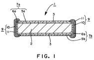
- Fig. 1 is a sectional view of a PTC element according to the present invention,
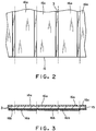
- Fig. 2 is a partial planar section of a PTC substrate, illustrating a process for producing a PTC element according to the present invention,
- Fig. 3 is a cross-sectional view of the substrate shown in Fig. 2,
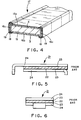
- Fig. 4 is an oblique view of a strip, illustrating a process for producing a PTC element according to the present invention,
- Fig. 5 is a side view of a conventional PTC element,
- Fig. 6 is a front view of a conventional PTC element, and
- Fig. 7 is a cross-sectional view of the substrate according to an embodiment of the present invention.
- A PTC element according to the present invention comprises an essentially plate-shaped PTC substrate, which is composed of a crystalline polymer having conductive particles dispersed therein; a pair of electrode films, preferably in the form of metallic foils, one of which is provided on each of the front and back surfaces of the PTC substrate; a pair of insulating layers, each of which covers one of the two opposing side faces of the PTC substrate and a part of one of the electrode films; and a pair of film-like electrodes provided on the surface of the insulating layers in such a manner as to be in electrical contact with the parts of the electrode films that are not covered by the insulating layers.
- PTC elements according to the instant invention are formed by bonding a pair of electrode films respectively to the front and back surfaces of an essentially plate-shaped PTC substrate which is formed of a PTC composition; providing a pair of insulating layers, each of which uninterruptedly covers each respective electrode film and one of the two opposing side faces of the PTC substrate in such a manner that a portion of the electrode film is exposed; and providing a pair of film-like electrodes on the surface of the insulating layers in such a manner as to be in electrical contact with the respective exposed portions of the pair of electrode films. It is thus possible to produce a small element comprising electrode films, insulating layers and a pair of electrodes with a sufficient insulation distance between the electrodes. The insulating layers may be formed by application of an insulating paste. As the electrodes are in the form of films and disposed at the side faces of the element, the element permits surface mounting in spite of its small size. The invention also permits easy production of PTC elements with improved productivity. Furthermore, the invention also ensures easy and reliable surface mounting, because the electrodes that extend from the front surface to the back surface of the PTC substrate permit surface mounting of the element to a printed board at the point where the electrodes face the printed board, and also at the points where the electrodes extend in a direction perpendicular to the printed board. Furthermore, the element can be mounted in either a face up or face down position.
- A PTC element according to the present invention may also possess a pair of side-face insulating layers provided on the respective two opposing sides of a PTC substrate, and a pair of surface insulating layers. Each of the surface insulating layers so covers one of the pair of electrode films respectively provided on the front surface and the back surface of the PTC substrate as to leave a portion of each electrode film exposed, each surface insulating layer and the adjacent side-face insulating layer being contiguous with each other. In other words, two insulating layers may be provided, each layer consisting of a surface insulating layer and a side-face insulating layer. The insulating layers may be formed by application of an insulating paste. As insulating layers can thus be easily applied, the invention is capable of easy production of PTC elements with improved productivity.
- A PTC element according to the present invention may have either the electrode films or the electrodes, or both, formed by application and sintering of conductive paste. The pair of electrodes may be provided by forming a pair of film-like conductive paste layers on the surface of the insulating layers with conductive paste such that the conductive paste layers are in contact with the portions where the pair of electrode films are exposed. Additionally, plating layers may be formed on the conductive paste layers. The PTC element may also include solder layers on the surface of the electrodes, and solder layers covering the surface of the electrode films. Therefore, easy and reliable soldering is ensured at the time of surface mounting of the element.
- A PTC element according to the present invention may have either the electrodes or the insulating layers, or both, formed by transfer printing of a pattern. This transfer printing may take the form of printing using an original plate with a curved surface on which the pattern is formed.
- Referring now to Fig. 1, a PTC element 1 includes a formed
body 2 composed of a crystalline polymer material having conductive particles dispersed therein. When used in a commercial electronic component, formedbody 2 should be so designed as to fit in the finished product. In other words, it should have a size slightly smaller than the finished product.Formed body 2 may be formed by any appropriate means, such as, for example, injection molding, extrusion, compression molding, or calendering. - A crystalline polymer material used to form a PTC element is typically one or a mixture of a plurality of known crystalline polymers having greater than 10% crystallinity. Examples of such crystalline polymers include high density polyethylene, middle density polyethylene, low density polyethylene, polypropylene, ethylene/propylene copolymers, polyolefins such as transpolybutadiene, fluorine polymers such as polytetrafluoroethylene and polyvinylidene fluoride, ethylene/acrylic acid copolymers, various polyesters, various polyamides and various polyethylene glycols. When used for overcurrent protection elements or other products that require a high positive temperature coefficient, the principal ingredient of the crystalline polymer material should preferably be a highly crystallized crystalline polymer, such as a polyethylene, and most preferably high density polyethylene. In the case of a product which does not require a high positive temperature coefficient, a polymer with a lower degree of crystallinity may be selected.
- As for conductive particles, a single type of various carbonaceous or metallic particles or a mixture of any combination of them may be used. Examples of usable materials include carbon black compounds such as furnace black, thermal black and acetylene black; carbonaceous particles such as graphite, carbon fiber and carbon beads; various metallic particles such as pure metal particles, particles of metal alloys or metal particles coated with another metal; and carbonaceous particles coated with metal. In order to obtain a high positive temperature coefficient, however, a carbon black compound is the most preferable material for conductive particles. Among various carbon blacks, low resistance thermal black exhibits an especially superior positive temperature coefficient. Conductive particles selected from the above group are dispersed in the crystalline polymer material by any appropriate means, such as, for example, thermal kneading on a roll mill or mixing in a Bambury mixer.
- A pair of
electrode films 3, in the form of metallic foils, are respectively bonded to the front and back surfaces, i. e. the upper and the lower surfaces as viewed in Fig. 1, of formedbody 2 by means of thermocompression bonding or compression molding.Electrode films 3 may be made of copper or nickel or an alloy of these metals, and preferably have a thickness of about 60 µm. -
Formed body 2 should preferably undergo cross-linking of the crystalline polymer material to stabilize the electrical resistance after manifestation of PTC characteristics. Cross-linking may be performed before or after the bonding ofelectrode films 3. Cross-linking may be performed by any appropriate means, such as, for example, irradiation by γ-rays or electron beams, followed by thermal aging. The crystalline polymer material may also be cross-linked chemically, instead of by irradiation. Further, to improve the reliability of PTC element 1, it is preferable to perform the thermal aging within the temperature range between the melting point and the decomposition point of the crystalline polymer material. - Film-like first and second
surface insulating layers electrode films 3. First surface insulatinglayer 5a and secondsurface insulating layer 5b are rotationally symmetrical around the center of formedbody 2, such that a portion of eachelectrode film 3 is exposed. Film-like first and second side-face insulating layers body 2. First side-face insulating layer 6a is contiguous with firstsurface insulating layer 5a, and second side-face insulating layer 6b is contiguous with secondsurface insulating layer 5b. First surface insulatinglayer 5a and first side-face insulating layer 6a integrally form a first insulatinglayer 7a. Secondsurface insulating layer 5b and second side-face insulating layer 6b integrally form a secondinsulating layer 7b. Thus, the outer surface of the pair ofelectrode films 3 and the two opposing ends (the right and left ends as viewed in Fig. 1) of formedbody 2 are covered by the pair of insulating layers, i. e. first insulatinglayer 7a and second insulatinglayer 7b, with a portion of eachelectrode film 3 exposed. First and second insulatinglayers layers layers - These insulating
layers layers - A thermosetting resin, such as epoxy resin, phenolic resin, unsaturated polyester or polyimide, is used as the insulating paste. These thermosetting resins have a high heat resistance and are in a fluid state at room temperature before hardening, making them easy to apply onto
electrode films 3. Taking into consideration the thermosetting temperature and heat resistance after setting, an epoxy resin type paste is preferable. - Where a thermosetting resin is used, heat curing is conducted under appropriate conditions to form first and second insulating
layers layer 7a and second insulatinglayer 7b after they are coated with the insulating paste, or the coating and heat curing steps may be performed for each insulating layer separately. - Still referring to Fig. 1, each of a pair of
electrodes 9 are formed on the two side faces of formedbody 2.Electrodes 9 have a thickness of, for example, 400 µm, or preferably 200 µm, or, even more preferably, 100 µm. Each of theseelectrodes 9 consist of aconductive film layer 10 and a plating layer 11. Conductive film layers 10 are layers of conductive paste respectively covering, first, the part ranging from the edge of the front surface of formedbody 2 over first side-face insulating layer 6a to the edge of the back surface of formedbody 2, and, second, the part ranging from the edge of the front surface of formedbody 2 over second side-face insulating layer 6b to the edge of the back surface of formedbody 2. In other words,conductive film layer 10 covering the outer surface of first side-face insulating layer 6a also covers the end portion of firstsurface insulating layer 5a, and partly covers the portion ofelectrode film 3 that is not covered by secondsurface insulating layer 5b. In a similar manner, the otherconductive film layer 10 covering the outer surface of second side-face insulating layer 6b also covers the end portion of firstsurface insulating layer 5a and partly covers the portion ofelectrode film 3 that is not covered by secondsurface insulating layer 5b. Plating layers 11 comprising nickel or another suitable metal plating cover conductive film layers 10. - Conductive film layers 10 are formed of conductive paste which is a mixture of conductive particles and a binder. Conductive particles used in this mixture should be similar to those used as the conductive particles in the PTC composition. Examples of appropriate materials for this purpose include particles of a metal as silver, palladium, gold, copper, aluminum, or nickel, or particles of other conductive materials, such as carbon black and graphite. The conductive particles used in this mixture are preferably silver. For the binder, a thermosetting resin, similar to the one used as the insulating paste, is most preferable. A heat resistant thermoplastic resin or the like may also be used. In addition to the conductive particles and the binder, other materials may be added to the conductive paste if desired. However, considering such factors as conductivity, heat resistance, reliability, hardening temperature, price and so forth, the combination of silver metal as the conductive particles and an epoxy resin as the resin is most preferable. After applying the conductive paste in the same manner as the insulating paste, a sintering treatment is performed to form conductive film layers 10.
-
Electrodes 9 may also be composed simply of conductive film layers 10. Alternatively,electrodes 9 may have a 2-layer structure, wherein a solder layer is formed on eachconductive film layer 10. Alternatively,electrodes 9 may have a 3-layer structure, wherein a solder layer is formed on each plating layer 11 that covers correspondingconductive film layer 10. Forming solder layers onrespective electrodes 9 facilitates soldering when PTC element 1 is mounted on a printed board. - Each surface of
electrode films 3, first insulatinglayer 7a, and second insulatinglayer 7b may be smooth or roughened. However, to improve the bonding strength to prevent peeling, the respective surfaces ofelectrode films 3 on which first and second insulatinglayers electrodes 9 are formed, and the surface of both first and second insulatinglayers - Referring now to Figs. 2 and 3, a PTC composition is prepared by dispersing conductive particles in a crystalline polymer material by means of, for example, thermal kneading on a roll mill or mixing in a Bambury mixer. Then, as shown in Figs. 2 and 3, the obtained PTC composition is formed into a thin, plate-shaped
substrate 15 having the length and width of, for example, 100 mm each by means of injection molding, extrusion, compression molding, calendering or any other appropriate method. Thereafter,electrode films 3, in the form of metallic foils, are bonded to the two opposing surfaces ofsubstrate 15 by means of thermo-compression, compression molding or any other appropriate method. The temperature for the compression molding should be set higher than the melting point of the crystalline polymer material in the PTC composition. Further,electrode films 3 may be bonded to the substrate when the substrate is formed. - The insulating paste then is applied in stripes by means of screen printing or a doctor blade on one of the surfaces of
substrate 15 whereelectrode films 3 are provided. After the insulating paste is allowed to dry, the paste is applied on the other surface and dried so that a plurality of insulatingpaste layers paste layers paste layer 16a is flush with the trailing edge of insulatingpaste layer 16b, as shown by the broken lines. - Next,
substrate 15 provided with insulating paste layers 16 and 16b is cut transversely along one of the longitudinal edges of each stripe of insulatingpaste layers strip 17 has a protruding exposed portion ofelectrode 3 on each of the front and back faces, and the exposed portions are diagonally opposite each other and substantially rotationally symmetrical about a longitudinal center axis. A variety of cutters, including a dicing saw, a shearing machine, or a laser may be used for this cutting operation. - Referring now to Fig. 4, insulating paste layers 16c are formed by applying the insulating paste onto both lateral edges of each
strip 17, i. e. the newly cut sides thereof, and drying the paste. Each insulatingpaste layer 16c is so formed as to cover the entire surface of one of the lateral edges of eachstrip 17, including the lateral ends ofelectrode films 3 and the corresponding end of either insulatingpaste layer paste layers 16c with conductive paste, using, for example, screen printing or a doctor blade. The conductive paste then is sintered. Eachconductive paste layer 18 has an essentially U-shaped section, with one of the two conductive paste layers 18 covering the part from the end of insulatingpaste layer 16a on the front surface to the exposed end ofelectrode film 3 that is not covered by insulatingpaste layer 16b on the back surface, and the otherconductive paste layer 18 covering the part from the end of insulatingpaste layer 16b on the back surface to the exposed end ofelectrode film 3 that is not covered by insulatingpaste layer 16a on the front surface. The surface of eachconductive paste layer 18 is plated with nickel or another appropriate metal, resulting in the formation of aplating film layer 19. - Next, by cutting each
strip 17 transversely by any appropriate cutting means, such as a dicing saw, a shearing machine, or a laser, along the lines represented by broken lines in Fig. 4, chip-shaped PTC elements 1 are obtained. Each transverse cut reveals anew electrode 9 on the end of each PTC element 1, formed by the cut throughconductive paste layer 18 andplating film layer 19 to formconductive layer 10 and plating layer 11, respectively. - In other words,
electrode films 3, insulatingpaste layers electrodes 9 that have a 2-layer structure consisting of conductive paste layers 18 and plating film layers 19 can be formed simply by applying a material for each layer in a film-like state. As described above, a plurality of chip-shaped PTC elements 1 be easily produced by simply cutting a plurality ofstrips 17, made in turn by cutting asubstrate 15, on which these layers are formed. Furthermore, PTC element chips produced in this way also permit surface mounting, because there is a sufficient insulation distance between the film-like electrodes 9 that are disposed at the respective two opposing side faces of each element. Thus, according to the invention, the productivity of such chip-shaped PTC elements can be improved. - Each
electrode 9 extends from the front surface to the back surface of formedbody 2. Therefore, when surface-mounting the PTC element onto a printed board, eachelectrode 9 is soldered to the printed board at the point where the electrode faces the printed board and also at the side of the PTC element where the electrode extends perpendicular to the printed board, thus ensuring easy and secure surface mounting. Furthermore, the element may be mounted either right side up or upside down. As a result, it is possible to produce a small overcurrent protection element which can be surface-mounted on a printed board. - The invention is explained referring to the above embodiment, wherein a
substrate 15 is cut into chips. However, chips may be produced through other procedures; for example,electrode films 3, a first insulatinglayer 7a, a secondinsulating layer 7b andelectrodes 9 may be formed on a formedbody 2 that has been formed beforehand in the size and the shape of a chip. Alternatively, asubstrate 15 havingelectrode films 3 with insulatingpaste layers - Although
electrode films 3 in the embodiment explained above are metallic foils,electrode films 3 may also be formed by application and sintering of conductive paste. Furthermore, first and secondsurface insulating layers face insulating layers electrodes 9 according to the embodiment explained above, a plurality of pairs ofelectrodes 9 may also be provided. - First, a PTC composition produced by dispersing carbon black in high density polyethylene was formed into pellets having a diameter not greater than 2 mm. Each pellet was placed in a die with nickel metal foils 3 having a thickness of 25 µm disposed at each of the two axial ends of the pellet. Compression molding was then conducted to form a
substrate 15 measuring 60 mm in length, 60 mm in width and 0.6mm in thickness. - Cross-linking was next conducted by irradiating
substrate 15 with 10 Mrad of γ-rays. An epoxy resin insulating paste was then screen-printed in stripes on one ofelectrode films 3 attached to both planar surfaces ofsubstrate 15, using a 165-mesh screen. Each printed pattern consisted of 10 stripes spaced 1 mm apart, and each stripe measured 3.8 mm in width and 55 mm in length. -
Substrate 15 was then placed in an oven at 120 °C to allow the insulating paste to dry and harden. Then, the same epoxy resin insulating paste was printed onelectrode film 3 attached to the opposite side ofsubstrate 15. The paste was printed in the same pattern, except that the pattern was staggered from the pattern on the first side by 1.0 mm in the widthwise direction. The insulating paste was dried and hardened in the same manner. - Next, using a shearing machine,
substrate 15 was cut along one of the two lengthwise edges of each stripe of insulatingpaste layer 16a on the front surface, i. e. the layer printed first. In thismanner 10strips 17 were formed, each strip measuring 60 mm in length, 4.8 mm in width and 1 mm in thickness. - Then, by using a 165-mesh screen, insulating paste composed of the same kind of insulating epoxy resin as that used for insulating
paste layers strip 17 was brought into surface-contact with the pattern printed on the plate, thus transferring the insulating paste onto the cut surface. The strip was then dried in an oven at 120 °C to allow the insulating paste to harden, so that an insulatingpaste layer 16c was formed on one of the two lateral sides ofstrip 17. An insulatingpaste layer 16c was then formed on the other side ofstrip 17 in the same manner. - Next, using a 60-mesh screen, solderable conductive paste composed of silver particles and epoxy resin was applied by printing on a flat surface of a glass plate, and one of the two side faces of
substrate 15, on which insulating paste layers 16c were formed, was submerged in the conductive paste. By holding the substrate in this position for 20 seconds, aconductive paste layer 18 is formed, having an essentially U-shaped cross-section extending from the exposed portion ofelectrode film 3 not covered by the insulating paste to the insulating paste layer on the back surface of the substrate. In the same manner, anotherconductive paste layer 18 having an essentially U-shaped section was formed over the surface of the other side face ofsubstrate 15. Conductive paste layers 18 were then dried and hardened in an oven at 150 °C. - After water soluble flux was applied to conductive paste layers 18 and the exposed portions of
electrode films 3,strip 17 was dipped in a solder bath containing #64 solder maintained at 260 °C. In this manner, a solder layer uninterruptedly covering conductive paste layers 18 and the exposed portions ofelectrode films 3 was formed. - Next, the parts which extended 1.25 mm from the respective lengthwise ends of the insulating paste layer formed on the electrodes of each
strip 17 were cut off and discarded. These are unnecessary parts where the material ofsubstrate 15 is exposed. Thereafter, eachstrip 17 was cut in the widthwise direction at 2.5 mm intervals to produce 20 chip-type PTC elements 1. In other words, a total of 200 PTC elements 1 were produced from asingle substrate 15. Each PTC element 1 measured about 5 mm in length, about 2.5 mm in width and about 0.7 mm in thickness. - PTC elements 1 were produced through the same procedure as above, except that conductive paste of a platable grade was used. In addition, the electrodes had a 3-layer structure including a plating layer and a solder layer. The plating layer was formed on the conductive paste layer by nickel plating, and the solder layer was formed on the plating layer by solder plating.
-
Strips 17 were made through the same procedure as that of the first embodiment described above. Then, solderable conductive paste of the same kind as that of the first embodiment was applied onto silicone rubber to form patterns each having the dimensions of 7 mm x 5.5 cm. The two side faces of eachstrip 17 were then pressed against these patterns to form conductive paste layers 18, having an essentially U-shaped cross-section extending from the exposed portion ofelectrode film 3 to an edge of one of insulatingpaste layer paste layers 16c. Then, the conductive paste layers were hardened in the same manner as the first embodiment.Strips 17 were then cut in the same manner as the first embodiment to obtain PTC elements 1. - As shown in Fig. 7,
substrate 15 may be cut along insulatingplate layer 16a in the middle part of insulatingplate layer 16a which are formed on the front surface ofelectrode film 3 and strips 17 are formed. In the similar manner,substrate 15 may be cut along insulatingplate layer 16b in the middle part of insulatingplate layer 16b which are formed on the back surface ofelectrode film 3 and strips 17 are formed. - Having described preferred embodiments of the invention with reference to the accompanying drawings, it is to be understood that the invention is not limited to those precise embodiments, and that various changes and modifications may be effected therein by one skilled in the art without departing from the scope or spirit of the invention as defined in the appended claims.
Claims (30)
- A PTC element, comprising:a substantially plate-shaped PTC substrate;a pair of electrode films, each of said pair of electrode films being provided at one of a front surface and a back surface of said PTC substrate;a pair of insulating layers, each of said insulating layers partially covering one of said pair of electrode films and leaving a portion of one of said pair of electrode films exposed, and completely covering one of a pair of side faces of said PTC substrate; anda pair of electrodes, each of said pair of electrodes being provided on a surface of said insulating layers such that said electrode is in electrical contact with said exposed portion of one of said pair of electrode films.
- A PTC element according to claim 1, wherein said pair of electrode films are in the form of metallic foils.
- A PTC element according to claim 1 or 2, wherein said exposed portions of said pair of electrode films are rotationally superimposable upon one another.
- A PTC element according to any preceding claim , wherein each of said pair of insulating layers uninterruptedly covers one of said pair of electrode films and one of said pair of side faces of said PTC substrate. any preceding
- A PTC element according to any preceding claim , wherein:said pair of insulating layers includes a pair of side-face insulating layers and a pair of surface insulating layers;each of said pair of side-face insulating layers covers one of said pair of side faces of said PTC substrate;each of said pair of side-face insulating layers is adjacent to one of said pair of surface insulating layers;each of said surface insulating layers partially covers one of said pair of electrode films, leaving a portion of said one of said pair of electrode films exposed; andeach surface insulating layer is contiguous with said one of said pair of side-face insulating layers adjacent to said surface insulating layer.
- A PTC element according to any preceding claim, wherein said insulating layers are formed by application of an insulating paste.
- A PTC element according to any preceding claim , wherein said pair of electrode films are formed by application and sintering of conductive paste.
- A PTC element according to any preceding claim , wherein said pair of electrodes are formed by application and sintering of conductive paste.
- A PTC element according to any preceding claim , further comprising plating layers formed on an outer surface of each of said pair of electrodes.
- A PTC element according to any preceding claim , wherein said pair of electrodes include solder layers provided on an outer surface of each of said pair of electrodes.
- A PTC element according to claim 9, wherein said pair of electrodes include solder layers provided on an outer surface of said plating layers.
- A PTC element according to any one of claims 1 to 7 or 9 to 11, wherein said pair of electrodes are formed by transfer printing of a pattern.
- A PTC element according to any one of claims 1 to 5 or 7 to 12, wherein said insulating layers are formed by transfer printing of a pattern.
- A PTC element according to any one of claims 1 to 7 or 9 to 11, wherein said pair of electrodes are formed by printing, using an original plate with a curved surface on which a pattern is formed.
- A PTC element according to any one of claims 1 to 5 or 7 to 12, wherein said insulating layers are formed by printing, using an original plate with a curved surface on which a pattern is formed.
- A PTC element according to any preceding claim , wherein said PTC substrate is formed of a crystalline polymer having conductive particles dispersed therein.
- A PTC element according to claim 16, wherein said crystalline polymer forming said PTC substrate is high density polyethylene.
- A PTC element according to any preceding claims, wherein said conductive particles are a carbon black.
- A PTC element according to any one of claims 2 to 18, wherein said metallic foil is one of the group consisting of copper, nickel, and an alloy of copper and nickel.
- A PTC element according to any preceding claim, wherein said insulating paste includes a thermosetting resin.
- A PTC element according to any preceding claim, wherein said insulating paste includes epoxy resin.
- A PTC element according to any preceding claim, wherein said electrodes include silver.
- A PTC element according to any preceding claim , wherein an outer surface of each of said electrode films is roughened.
- A PTC element according to any preceding claim , wherein an outer surface of each of said insulating layers is roughened.
- A method of producing a PTC element, comprising the steps of:dispersing conductive particles in a crystalline polymer material;forming said crystalline polymer material having said conductive particles dispersed therein into a shape, said shape having a pair of opposing surfaces;bonding an electrode film to each of said pair of opposing surfaces;forming a first plurality of stripes of insulating material on one of said electrode films;forming a second plurality of stripes of insulating material on another of said electrode films, said second plurality of stripes running in a first direction along said substrate identical to that of said first plurality of stripes, and being offset from said first plurality of stripes in a second direction perpendicular to said first direction to form a staggered alignment of said first and said second plurality of stripes;cutting said crystalline polymer material parallel to a longitudinal edge of each of one of said first and said second plurality of stripes, thereby forming a plurality of strips, each of said plurality of strips having a pair of opposing side faces and a portion of each of said electrode films exposed;forming a layer of insulating material along each of said pair of opposing side faces;forming a layer of conductive material along an outer surface of said layer of insulating material applied along each of said pair of opposing side faces, such that said layer of conductive material along each outer surface has a U-shaped cross-section and covers from an end of said layer of insulating material to said exposed portion of one of said electrode films; andcutting each of said plurality of strips laterally to divide said strip into finished chip-shaped PTC elements.
- A method according to claim 25, wherein said first and said second plurality of stripes of said insulating material are formed by applying insulating paste on each of said electrode films, and drying and hardening said insulating paste. or 26
- A method according to claim 25 or 26, wherein said layer of insulating material along each of said pair of opposing side faces is formed by applying insulating paste, and drying and hardening said insulating paste.
- A method according to any one of claims 25 to 27, wherein said layer of conductive material is formed by applying conductive paste, and sintering said conductive paste.
- A method as claimed in any one of claims 25 to 28 as applied to the production of a PTC element as claimed in any one of claims 1 to 24.
- Use of a PTC element as claimed in any one of claims 1 to 24, or when obtained by a method according to claim 29, as an overcurrent protection device in a product.
Applications Claiming Priority (2)
| Application Number | Priority Date | Filing Date | Title |
|---|---|---|---|
| JP2570296A JPH09219302A (en) | 1996-02-13 | 1996-02-13 | Ptc element |
| JP25702/96 | 1996-02-13 |
Publications (2)
| Publication Number | Publication Date |
|---|---|
| EP0790625A2 true EP0790625A2 (en) | 1997-08-20 |
| EP0790625A3 EP0790625A3 (en) | 1998-07-29 |
Family
ID=12173129
Family Applications (1)
| Application Number | Title | Priority Date | Filing Date |
|---|---|---|---|
| EP97300947A Withdrawn EP0790625A3 (en) | 1996-02-13 | 1997-02-13 | PTC element |
Country Status (2)
| Country | Link |
|---|---|
| EP (1) | EP0790625A3 (en) |
| JP (1) | JPH09219302A (en) |
Cited By (8)
| Publication number | Priority date | Publication date | Assignee | Title |
|---|---|---|---|---|
| WO1997045845A1 (en) * | 1996-05-30 | 1997-12-04 | Littelfuse, Inc. | Ptc circuit protection device |
| EP0901133A2 (en) * | 1997-09-03 | 1999-03-10 | Bourns Multifuse (Hong Kong), Ltd. | Multilayer conductive polymer positive temperature coefficient device |
| WO1999053505A1 (en) * | 1998-04-14 | 1999-10-21 | Tyco Electronics Corporation | Electrical devices |
| EP1073068A1 (en) * | 1998-04-09 | 2001-01-31 | Matsushita Electric Industrial Co., Ltd. | Ptc thermistor chip |
| WO2002032497A1 (en) * | 2000-10-20 | 2002-04-25 | Advanced Metal Coatings Pty Limited | An electrical lead |
| US6522237B1 (en) | 1999-05-10 | 2003-02-18 | Matsushita Electric Industrial Co., Ltd. | Electrode for PTC thermistor and method for producing the same, and PTC thermistor |
| EP1701391A1 (en) * | 2003-12-26 | 2006-09-13 | Murata Manufacturing Co., Ltd. | Thick-film electrode and multilayer ceramic electronic component |
| US8286338B2 (en) | 2004-08-05 | 2012-10-16 | Cathrx Ltd | Process of manufacturing a medical use electrical lead |
Families Citing this family (6)
| Publication number | Priority date | Publication date | Assignee | Title |
|---|---|---|---|---|
| US6582647B1 (en) | 1998-10-01 | 2003-06-24 | Littelfuse, Inc. | Method for heat treating PTC devices |
| US6640420B1 (en) | 1999-09-14 | 2003-11-04 | Tyco Electronics Corporation | Process for manufacturing a composite polymeric circuit protection device |
| JP3628222B2 (en) * | 2000-01-14 | 2005-03-09 | ソニーケミカル株式会社 | Manufacturing method of PTC element |
| US6628498B2 (en) | 2000-08-28 | 2003-09-30 | Steven J. Whitney | Integrated electrostatic discharge and overcurrent device |
| JP3827514B2 (en) * | 2000-09-29 | 2006-09-27 | Tdk株式会社 | Polymer PTC element |
| CN104392938B (en) * | 2014-10-29 | 2017-04-19 | 禾邦电子(苏州)有限公司 | semiconductor chip packaging method |
Citations (5)
| Publication number | Priority date | Publication date | Assignee | Title |
|---|---|---|---|---|
| EP0229286A1 (en) * | 1985-12-17 | 1987-07-22 | Siemens Aktiengesellschaft | Electrical component in the form of a chip |
| US4787135A (en) * | 1986-03-31 | 1988-11-29 | Nippon Mektron, Ltd. | Method of attaching leads to PTC devices |
| EP0336497A1 (en) * | 1988-04-05 | 1989-10-11 | Koninklijke Philips Electronics N.V. | Method of manufacturing a chip resistor |
| US4959632A (en) * | 1988-04-06 | 1990-09-25 | Murata Manufacturing Co., Ltd. | Organic PTC thermistor |
| WO1995034084A1 (en) * | 1994-06-09 | 1995-12-14 | Raychem Corporation | Electrical devices |
-
1996
- 1996-02-13 JP JP2570296A patent/JPH09219302A/en active Pending
-
1997
- 1997-02-13 EP EP97300947A patent/EP0790625A3/en not_active Withdrawn
Patent Citations (5)
| Publication number | Priority date | Publication date | Assignee | Title |
|---|---|---|---|---|
| EP0229286A1 (en) * | 1985-12-17 | 1987-07-22 | Siemens Aktiengesellschaft | Electrical component in the form of a chip |
| US4787135A (en) * | 1986-03-31 | 1988-11-29 | Nippon Mektron, Ltd. | Method of attaching leads to PTC devices |
| EP0336497A1 (en) * | 1988-04-05 | 1989-10-11 | Koninklijke Philips Electronics N.V. | Method of manufacturing a chip resistor |
| US4959632A (en) * | 1988-04-06 | 1990-09-25 | Murata Manufacturing Co., Ltd. | Organic PTC thermistor |
| WO1995034084A1 (en) * | 1994-06-09 | 1995-12-14 | Raychem Corporation | Electrical devices |
Cited By (18)
| Publication number | Priority date | Publication date | Assignee | Title |
|---|---|---|---|---|
| WO1997045845A1 (en) * | 1996-05-30 | 1997-12-04 | Littelfuse, Inc. | Ptc circuit protection device |
| EP0901133A2 (en) * | 1997-09-03 | 1999-03-10 | Bourns Multifuse (Hong Kong), Ltd. | Multilayer conductive polymer positive temperature coefficient device |
| EP0901133A3 (en) * | 1997-09-03 | 1999-07-07 | Bourns Multifuse (Hong Kong), Ltd. | Multilayer conductive polymer positive temperature coefficient device |
| EP1073068A4 (en) * | 1998-04-09 | 2007-05-02 | Matsushita Electric Ind Co Ltd | Ptc thermistor chip |
| EP1073068A1 (en) * | 1998-04-09 | 2001-01-31 | Matsushita Electric Industrial Co., Ltd. | Ptc thermistor chip |
| US6606023B2 (en) | 1998-04-14 | 2003-08-12 | Tyco Electronics Corporation | Electrical devices |
| US7053748B2 (en) | 1998-04-14 | 2006-05-30 | Tyco Electronics Corporation | Electrical devices |
| WO1999053505A1 (en) * | 1998-04-14 | 1999-10-21 | Tyco Electronics Corporation | Electrical devices |
| US6522237B1 (en) | 1999-05-10 | 2003-02-18 | Matsushita Electric Industrial Co., Ltd. | Electrode for PTC thermistor and method for producing the same, and PTC thermistor |
| US6558616B2 (en) | 1999-05-10 | 2003-05-06 | Matsushita Electric Industrial Co., Ltd. | Electrode for PTC thermistor and method for producing the same, and PTC thermistor |
| WO2002032497A1 (en) * | 2000-10-20 | 2002-04-25 | Advanced Metal Coatings Pty Limited | An electrical lead |
| US7625617B1 (en) | 2000-10-20 | 2009-12-01 | Cathrx Ltd | Electrical lead |
| US7629015B2 (en) | 2000-10-20 | 2009-12-08 | Cathrx Ltd | Method of manufacturing an electrical lead |
| US8075969B2 (en) | 2000-10-20 | 2011-12-13 | Cathrx Ltd | Electrical lead |
| EP1701391A1 (en) * | 2003-12-26 | 2006-09-13 | Murata Manufacturing Co., Ltd. | Thick-film electrode and multilayer ceramic electronic component |
| EP1701391A4 (en) * | 2003-12-26 | 2009-12-30 | Murata Manufacturing Co | Thick-film electrode and multilayer ceramic electronic component |
| US8286338B2 (en) | 2004-08-05 | 2012-10-16 | Cathrx Ltd | Process of manufacturing a medical use electrical lead |
| US10668275B2 (en) | 2004-08-05 | 2020-06-02 | Cathrx Ltd | Electrical leads for medical use |
Also Published As
| Publication number | Publication date |
|---|---|
| JPH09219302A (en) | 1997-08-19 |
| EP0790625A3 (en) | 1998-07-29 |
Similar Documents
| Publication | Publication Date | Title |
|---|---|---|
| US5351390A (en) | Manufacturing method for a PTC thermistor | |
| US7355504B2 (en) | Electrical devices | |
| EP0790625A2 (en) | PTC element | |
| EP0719442B1 (en) | Electrical assembly comprising a ptc resistive element | |
| US7053748B2 (en) | Electrical devices | |
| JP4666760B2 (en) | Electrical device using conductive polymer | |
| US5884391A (en) | Process for manufacturing an electrical device comprising a PTC element | |
| EP0811993B1 (en) | Electrical devices | |
| US5257003A (en) | Thermistor and its method of manufacture | |
| DE3910861A1 (en) | ORGANIC PTC THERMISTOR | |
| JP3628222B2 (en) | Manufacturing method of PTC element | |
| KR950015004B1 (en) | Ptc thermister and manufacturing method thereof | |
| JPH09320808A (en) | Ptc thermistor | |
| JP2004288956A (en) | Chip electronic component | |
| JP3820825B2 (en) | PTC thermistor | |
| JPH1187105A (en) | Ptc element | |
| JPH10289806A (en) | Ptc element | |
| JPH09199302A (en) | Chip thermistor and its manufacture | |
| JPH0363233B2 (en) | ||
| JPH09246013A (en) | Chip ptc thermistor | |
| JP2004111459A (en) | Chip-form electronic component | |
| JPS59224088A (en) | Panel heater | |
| JPH09129406A (en) | Electronic component and manufacture thereof | |
| JPH09120905A (en) | Chip electronic part and method for manufacturing the same | |
| JPH03284812A (en) | Chip type ceramic capacitor |
Legal Events
| Date | Code | Title | Description |
|---|---|---|---|
| PUAI | Public reference made under article 153(3) epc to a published international application that has entered the european phase |
Free format text: ORIGINAL CODE: 0009012 |
|
| AK | Designated contracting states |
Kind code of ref document: A2 Designated state(s): DE FR GB NL |
|
| PUAL | Search report despatched |
Free format text: ORIGINAL CODE: 0009013 |
|
| AK | Designated contracting states |
Kind code of ref document: A3 Designated state(s): DE FR GB NL |
|
| STAA | Information on the status of an ep patent application or granted ep patent |
Free format text: STATUS: THE APPLICATION IS DEEMED TO BE WITHDRAWN |
|
| 18D | Application deemed to be withdrawn |
Effective date: 19990130 |