EP0807973A2 - Plastic molded type semiconductor device and method of manufacturing the same - Google Patents
Plastic molded type semiconductor device and method of manufacturing the same Download PDFInfo
- Publication number
- EP0807973A2 EP0807973A2 EP97302914A EP97302914A EP0807973A2 EP 0807973 A2 EP0807973 A2 EP 0807973A2 EP 97302914 A EP97302914 A EP 97302914A EP 97302914 A EP97302914 A EP 97302914A EP 0807973 A2 EP0807973 A2 EP 0807973A2
- Authority
- EP
- European Patent Office
- Prior art keywords
- dambar
- semiconductor element
- leads
- adhesive tape
- lead frame
- Prior art date
- Legal status (The legal status is an assumption and is not a legal conclusion. Google has not performed a legal analysis and makes no representation as to the accuracy of the status listed.)
- Granted
Links
- 239000004065 semiconductor Substances 0.000 title claims abstract description 296
- 238000004519 manufacturing process Methods 0.000 title claims abstract description 58
- 239000004033 plastic Substances 0.000 title claims abstract description 34
- 239000011347 resin Substances 0.000 claims abstract description 122
- 229920005989 resin Polymers 0.000 claims abstract description 122
- 239000002390 adhesive tape Substances 0.000 claims description 96
- 238000000034 method Methods 0.000 claims description 20
- 238000007789 sealing Methods 0.000 claims description 19
- 239000000463 material Substances 0.000 claims description 17
- 238000000576 coating method Methods 0.000 claims description 14
- PCHJSUWPFVWCPO-UHFFFAOYSA-N gold Chemical compound [Au] PCHJSUWPFVWCPO-UHFFFAOYSA-N 0.000 claims description 14
- 239000010931 gold Substances 0.000 claims description 14
- 229910052737 gold Inorganic materials 0.000 claims description 14
- 239000011248 coating agent Substances 0.000 claims description 13
- 239000012790 adhesive layer Substances 0.000 claims description 10
- 239000007788 liquid Substances 0.000 claims description 5
- 239000003566 sealing material Substances 0.000 claims 2
- 238000001035 drying Methods 0.000 claims 1
- 238000007654 immersion Methods 0.000 claims 1
- 230000004048 modification Effects 0.000 description 66
- 238000012986 modification Methods 0.000 description 66
- 238000000465 moulding Methods 0.000 description 13
- 239000002184 metal Substances 0.000 description 12
- 229910052751 metal Inorganic materials 0.000 description 12
- 229910000679 solder Inorganic materials 0.000 description 12
- 238000007747 plating Methods 0.000 description 10
- 238000007872 degassing Methods 0.000 description 8
- 238000002347 injection Methods 0.000 description 6
- 239000007924 injection Substances 0.000 description 6
- 230000008569 process Effects 0.000 description 6
- 230000006835 compression Effects 0.000 description 4
- 238000007906 compression Methods 0.000 description 4
- 238000002844 melting Methods 0.000 description 4
- 230000008018 melting Effects 0.000 description 4
- 238000012856 packing Methods 0.000 description 4
- 238000012545 processing Methods 0.000 description 4
- 230000002093 peripheral effect Effects 0.000 description 3
- 230000008646 thermal stress Effects 0.000 description 3
- 230000015572 biosynthetic process Effects 0.000 description 2
- 239000000919 ceramic Substances 0.000 description 2
- 230000008878 coupling Effects 0.000 description 2
- 238000010168 coupling process Methods 0.000 description 2
- 238000005859 coupling reaction Methods 0.000 description 2
- 238000005530 etching Methods 0.000 description 2
- 230000006870 function Effects 0.000 description 2
- 230000001771 impaired effect Effects 0.000 description 2
- 239000012535 impurity Substances 0.000 description 2
- 229920001721 polyimide Polymers 0.000 description 2
- 239000009719 polyimide resin Substances 0.000 description 2
- 230000009467 reduction Effects 0.000 description 2
- 229910052710 silicon Inorganic materials 0.000 description 2
- 239000010703 silicon Substances 0.000 description 2
- 239000000758 substrate Substances 0.000 description 2
- 238000009423 ventilation Methods 0.000 description 2
- 238000005452 bending Methods 0.000 description 1
- 230000000740 bleeding effect Effects 0.000 description 1
- 238000004891 communication Methods 0.000 description 1
- 238000007599 discharging Methods 0.000 description 1
- 230000000694 effects Effects 0.000 description 1
- 239000003822 epoxy resin Substances 0.000 description 1
- 238000000605 extraction Methods 0.000 description 1
- 229920000647 polyepoxide Polymers 0.000 description 1
- 230000002265 prevention Effects 0.000 description 1
- 239000002904 solvent Substances 0.000 description 1
Images


Classifications
-
- H—ELECTRICITY
- H01—ELECTRIC ELEMENTS
- H01L—SEMICONDUCTOR DEVICES NOT COVERED BY CLASS H10
- H01L21/00—Processes or apparatus adapted for the manufacture or treatment of semiconductor or solid state devices or of parts thereof
- H01L21/02—Manufacture or treatment of semiconductor devices or of parts thereof
- H01L21/04—Manufacture or treatment of semiconductor devices or of parts thereof the devices having at least one potential-jump barrier or surface barrier, e.g. PN junction, depletion layer or carrier concentration layer
- H01L21/50—Assembly of semiconductor devices using processes or apparatus not provided for in a single one of the subgroups H01L21/06 - H01L21/326, e.g. sealing of a cap to a base of a container
- H01L21/56—Encapsulations, e.g. encapsulation layers, coatings
- H01L21/565—Moulds
-
- H—ELECTRICITY
- H01—ELECTRIC ELEMENTS
- H01L—SEMICONDUCTOR DEVICES NOT COVERED BY CLASS H10
- H01L21/00—Processes or apparatus adapted for the manufacture or treatment of semiconductor or solid state devices or of parts thereof
- H01L21/02—Manufacture or treatment of semiconductor devices or of parts thereof
- H01L21/04—Manufacture or treatment of semiconductor devices or of parts thereof the devices having at least one potential-jump barrier or surface barrier, e.g. PN junction, depletion layer or carrier concentration layer
- H01L21/50—Assembly of semiconductor devices using processes or apparatus not provided for in a single one of the subgroups H01L21/06 - H01L21/326, e.g. sealing of a cap to a base of a container
- H01L21/60—Attaching or detaching leads or other conductive members, to be used for carrying current to or from the device in operation
-
- H—ELECTRICITY
- H01—ELECTRIC ELEMENTS
- H01L—SEMICONDUCTOR DEVICES NOT COVERED BY CLASS H10
- H01L23/00—Details of semiconductor or other solid state devices
- H01L23/28—Encapsulations, e.g. encapsulating layers, coatings, e.g. for protection
- H01L23/31—Encapsulations, e.g. encapsulating layers, coatings, e.g. for protection characterised by the arrangement or shape
- H01L23/3107—Encapsulations, e.g. encapsulating layers, coatings, e.g. for protection characterised by the arrangement or shape the device being completely enclosed
- H01L23/3114—Encapsulations, e.g. encapsulating layers, coatings, e.g. for protection characterised by the arrangement or shape the device being completely enclosed the device being a chip scale package, e.g. CSP
-
- H—ELECTRICITY
- H01—ELECTRIC ELEMENTS
- H01L—SEMICONDUCTOR DEVICES NOT COVERED BY CLASS H10
- H01L23/00—Details of semiconductor or other solid state devices
- H01L23/48—Arrangements for conducting electric current to or from the solid state body in operation, e.g. leads, terminal arrangements ; Selection of materials therefor
- H01L23/488—Arrangements for conducting electric current to or from the solid state body in operation, e.g. leads, terminal arrangements ; Selection of materials therefor consisting of soldered or bonded constructions
- H01L23/495—Lead-frames or other flat leads
- H01L23/49503—Lead-frames or other flat leads characterised by the die pad
- H01L23/4951—Chip-on-leads or leads-on-chip techniques, i.e. inner lead fingers being used as die pad
-
- H—ELECTRICITY
- H01—ELECTRIC ELEMENTS
- H01L—SEMICONDUCTOR DEVICES NOT COVERED BY CLASS H10
- H01L2224/00—Indexing scheme for arrangements for connecting or disconnecting semiconductor or solid-state bodies and methods related thereto as covered by H01L24/00
- H01L2224/01—Means for bonding being attached to, or being formed on, the surface to be connected, e.g. chip-to-package, die-attach, "first-level" interconnects; Manufacturing methods related thereto
- H01L2224/42—Wire connectors; Manufacturing methods related thereto
- H01L2224/44—Structure, shape, material or disposition of the wire connectors prior to the connecting process
- H01L2224/45—Structure, shape, material or disposition of the wire connectors prior to the connecting process of an individual wire connector
- H01L2224/45001—Core members of the connector
- H01L2224/45099—Material
- H01L2224/451—Material with a principal constituent of the material being a metal or a metalloid, e.g. boron (B), silicon (Si), germanium (Ge), arsenic (As), antimony (Sb), tellurium (Te) and polonium (Po), and alloys thereof
- H01L2224/45138—Material with a principal constituent of the material being a metal or a metalloid, e.g. boron (B), silicon (Si), germanium (Ge), arsenic (As), antimony (Sb), tellurium (Te) and polonium (Po), and alloys thereof the principal constituent melting at a temperature of greater than or equal to 950°C and less than 1550°C
- H01L2224/45144—Gold (Au) as principal constituent
-
- H—ELECTRICITY
- H01—ELECTRIC ELEMENTS
- H01L—SEMICONDUCTOR DEVICES NOT COVERED BY CLASS H10
- H01L2224/00—Indexing scheme for arrangements for connecting or disconnecting semiconductor or solid-state bodies and methods related thereto as covered by H01L24/00
- H01L2224/01—Means for bonding being attached to, or being formed on, the surface to be connected, e.g. chip-to-package, die-attach, "first-level" interconnects; Manufacturing methods related thereto
- H01L2224/42—Wire connectors; Manufacturing methods related thereto
- H01L2224/47—Structure, shape, material or disposition of the wire connectors after the connecting process
- H01L2224/48—Structure, shape, material or disposition of the wire connectors after the connecting process of an individual wire connector
- H01L2224/4805—Shape
- H01L2224/4809—Loop shape
- H01L2224/48091—Arched
-
- H—ELECTRICITY
- H01—ELECTRIC ELEMENTS
- H01L—SEMICONDUCTOR DEVICES NOT COVERED BY CLASS H10
- H01L2224/00—Indexing scheme for arrangements for connecting or disconnecting semiconductor or solid-state bodies and methods related thereto as covered by H01L24/00
- H01L2224/01—Means for bonding being attached to, or being formed on, the surface to be connected, e.g. chip-to-package, die-attach, "first-level" interconnects; Manufacturing methods related thereto
- H01L2224/42—Wire connectors; Manufacturing methods related thereto
- H01L2224/47—Structure, shape, material or disposition of the wire connectors after the connecting process
- H01L2224/48—Structure, shape, material or disposition of the wire connectors after the connecting process of an individual wire connector
- H01L2224/481—Disposition
- H01L2224/48151—Connecting between a semiconductor or solid-state body and an item not being a semiconductor or solid-state body, e.g. chip-to-substrate, chip-to-passive
- H01L2224/48221—Connecting between a semiconductor or solid-state body and an item not being a semiconductor or solid-state body, e.g. chip-to-substrate, chip-to-passive the body and the item being stacked
- H01L2224/48245—Connecting between a semiconductor or solid-state body and an item not being a semiconductor or solid-state body, e.g. chip-to-substrate, chip-to-passive the body and the item being stacked the item being metallic
- H01L2224/48247—Connecting between a semiconductor or solid-state body and an item not being a semiconductor or solid-state body, e.g. chip-to-substrate, chip-to-passive the body and the item being stacked the item being metallic connecting the wire to a bond pad of the item
-
- H—ELECTRICITY
- H01—ELECTRIC ELEMENTS
- H01L—SEMICONDUCTOR DEVICES NOT COVERED BY CLASS H10
- H01L2224/00—Indexing scheme for arrangements for connecting or disconnecting semiconductor or solid-state bodies and methods related thereto as covered by H01L24/00
- H01L2224/01—Means for bonding being attached to, or being formed on, the surface to be connected, e.g. chip-to-package, die-attach, "first-level" interconnects; Manufacturing methods related thereto
- H01L2224/42—Wire connectors; Manufacturing methods related thereto
- H01L2224/47—Structure, shape, material or disposition of the wire connectors after the connecting process
- H01L2224/48—Structure, shape, material or disposition of the wire connectors after the connecting process of an individual wire connector
- H01L2224/481—Disposition
- H01L2224/48151—Connecting between a semiconductor or solid-state body and an item not being a semiconductor or solid-state body, e.g. chip-to-substrate, chip-to-passive
- H01L2224/48221—Connecting between a semiconductor or solid-state body and an item not being a semiconductor or solid-state body, e.g. chip-to-substrate, chip-to-passive the body and the item being stacked
- H01L2224/48245—Connecting between a semiconductor or solid-state body and an item not being a semiconductor or solid-state body, e.g. chip-to-substrate, chip-to-passive the body and the item being stacked the item being metallic
- H01L2224/4826—Connecting between the body and an opposite side of the item with respect to the body
-
- H—ELECTRICITY
- H01—ELECTRIC ELEMENTS
- H01L—SEMICONDUCTOR DEVICES NOT COVERED BY CLASS H10
- H01L2224/00—Indexing scheme for arrangements for connecting or disconnecting semiconductor or solid-state bodies and methods related thereto as covered by H01L24/00
- H01L2224/01—Means for bonding being attached to, or being formed on, the surface to be connected, e.g. chip-to-package, die-attach, "first-level" interconnects; Manufacturing methods related thereto
- H01L2224/42—Wire connectors; Manufacturing methods related thereto
- H01L2224/47—Structure, shape, material or disposition of the wire connectors after the connecting process
- H01L2224/48—Structure, shape, material or disposition of the wire connectors after the connecting process of an individual wire connector
- H01L2224/484—Connecting portions
- H01L2224/48463—Connecting portions the connecting portion on the bonding area of the semiconductor or solid-state body being a ball bond
- H01L2224/48465—Connecting portions the connecting portion on the bonding area of the semiconductor or solid-state body being a ball bond the other connecting portion not on the bonding area being a wedge bond, i.e. ball-to-wedge, regular stitch
-
- H—ELECTRICITY
- H01—ELECTRIC ELEMENTS
- H01L—SEMICONDUCTOR DEVICES NOT COVERED BY CLASS H10
- H01L24/00—Arrangements for connecting or disconnecting semiconductor or solid-state bodies; Methods or apparatus related thereto
- H01L24/01—Means for bonding being attached to, or being formed on, the surface to be connected, e.g. chip-to-package, die-attach, "first-level" interconnects; Manufacturing methods related thereto
- H01L24/42—Wire connectors; Manufacturing methods related thereto
- H01L24/44—Structure, shape, material or disposition of the wire connectors prior to the connecting process
- H01L24/45—Structure, shape, material or disposition of the wire connectors prior to the connecting process of an individual wire connector
-
- H—ELECTRICITY
- H01—ELECTRIC ELEMENTS
- H01L—SEMICONDUCTOR DEVICES NOT COVERED BY CLASS H10
- H01L24/00—Arrangements for connecting or disconnecting semiconductor or solid-state bodies; Methods or apparatus related thereto
- H01L24/01—Means for bonding being attached to, or being formed on, the surface to be connected, e.g. chip-to-package, die-attach, "first-level" interconnects; Manufacturing methods related thereto
- H01L24/42—Wire connectors; Manufacturing methods related thereto
- H01L24/47—Structure, shape, material or disposition of the wire connectors after the connecting process
- H01L24/48—Structure, shape, material or disposition of the wire connectors after the connecting process of an individual wire connector
-
- H—ELECTRICITY
- H01—ELECTRIC ELEMENTS
- H01L—SEMICONDUCTOR DEVICES NOT COVERED BY CLASS H10
- H01L2924/00—Indexing scheme for arrangements or methods for connecting or disconnecting semiconductor or solid-state bodies as covered by H01L24/00
- H01L2924/01—Chemical elements
- H01L2924/01078—Platinum [Pt]
-
- H—ELECTRICITY
- H01—ELECTRIC ELEMENTS
- H01L—SEMICONDUCTOR DEVICES NOT COVERED BY CLASS H10
- H01L2924/00—Indexing scheme for arrangements or methods for connecting or disconnecting semiconductor or solid-state bodies as covered by H01L24/00
- H01L2924/01—Chemical elements
- H01L2924/01079—Gold [Au]
-
- H—ELECTRICITY
- H01—ELECTRIC ELEMENTS
- H01L—SEMICONDUCTOR DEVICES NOT COVERED BY CLASS H10
- H01L2924/00—Indexing scheme for arrangements or methods for connecting or disconnecting semiconductor or solid-state bodies as covered by H01L24/00
- H01L2924/06—Polymers
- H01L2924/078—Adhesive characteristics other than chemical
- H01L2924/07802—Adhesive characteristics other than chemical not being an ohmic electrical conductor
-
- H—ELECTRICITY
- H01—ELECTRIC ELEMENTS
- H01L—SEMICONDUCTOR DEVICES NOT COVERED BY CLASS H10
- H01L2924/00—Indexing scheme for arrangements or methods for connecting or disconnecting semiconductor or solid-state bodies as covered by H01L24/00
- H01L2924/10—Details of semiconductor or other solid state devices to be connected
- H01L2924/11—Device type
- H01L2924/14—Integrated circuits
Landscapes
- Engineering & Computer Science (AREA)
- Microelectronics & Electronic Packaging (AREA)
- Physics & Mathematics (AREA)
- Condensed Matter Physics & Semiconductors (AREA)
- General Physics & Mathematics (AREA)
- Computer Hardware Design (AREA)
- Power Engineering (AREA)
- Manufacturing & Machinery (AREA)
- Encapsulation Of And Coatings For Semiconductor Or Solid State Devices (AREA)
- Structures Or Materials For Encapsulating Or Coating Semiconductor Devices Or Solid State Devices (AREA)
Abstract
Description
- This invention relates to a plastic molded type semiconductor device and a method of manufacturing it.
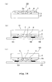
- With rapid advances in IC and memory cards, there has recently been a demand for thin ones as plastic molded type semiconductor devices installed in the cards. As methods of realizing the thin-type semiconductor devices, a vast number of proposals have been made. One example of structures of the semiconductor devices is shown in Figs. 25(a) and 25(b).
- In Figs. 25(a) and 25(b), reference numeral 1 indicates a plastic molded type semiconductor device and
reference numeral 2 indicates a semiconductor element. Thesemiconductor element 2 has one surface to which achip support 4 is bonded and fixed by an insulatingadhesive tape 3. Further,leads 6 are electrically connected to thesemiconductor element 2 throughgold wires 5 connected to both sides of thechip support 4. The plastic molded type semiconductor device 1 is formed by sealing thesemiconductor element 2 with amold resin 7 so that the upper surface of thechip support 4 and the bottom face of thesemiconductor element 2 are exposed. - According to such a structure, since the bottom face of the
semiconductor element 2 is not covered with themold resin 7 in particular, the semiconductor device can be made thin correspondingly. - However, if consideration is given to an area for the implementation of the semiconductor device 1 on a printed board even though the thickness of the plastic molded type semiconductor device 1 can be thinned, an area much wider than the size of the
semiconductor element 2 is required as its implementation area because theleads 6 extend long toward the outside of themold resin 7. Thus, if the implementation of the plastic molded type semiconductor device 1 on the printed board is taken into consideration, then problems to be improved still remain to realize more densely packing. - With the foregoing in view, it is an object of the present invention to provide a plastic molded type semiconductor device capable of being more densely implemented on a printed board and a method of manufacturing the semiconductor device. The plastic molded type semiconductor device of the present invention comprises a semiconductor element having electrodes provided on a surface thereof, a dambar formed along the outer periphery of the surface of the semiconductor element, a plurality of leads respectively electrically connected to the electrodes and provided inside the dambar electrically independent of the dambar, and a mold resin formed within a region surrounded by the dambar and formed so as to expose parts of the leads.
- In order to achieve the above object, there is provided a plastic molded type semiconductor device of the present invention, comprising:
- a semiconductor element having electrodes provided on a surface thereof;
- a dambar formed along the outer periphery of the surface of the semiconductor element;
- a plurality of leads respectively electrically connected to the electrodes and provided inside the dambar electrically independent of the dambar; and
- a mold resin formed within a region surrounded by the dambar and formed so as to expose parts of the leads.
- Typical ones of various inventions of the present application have been shown in brief. However, the various inventions of the present application and specific configurations of these inventions will be understood from the following description.
- While the specification concludes with claims particularly pointing out and distinctly claiming the subject matter which is regarded as the invention, it is believed that the invention, the objects and features of the invention and further objects, features and advantages thereof will be better understood from the following description taken in connection with the accompanying drawings in which:
- Fig. 1 schematically shows the configuration of a first embodiment of a plastic molded type semiconductor device of the present invention, wherein Fig. 1(a) is a cross-sectional side view of the first embodiment and Fig. 1(b) is a perspective view of the first embodiment;
- Fig. 2 illustrates a method of manufacturing the semiconductor device shown in Fig. 1, wherein Fig. 2(a) is a plan view schematically showing the configuration of a prepared lead frame, Fig. 2(b) is a plan view schematically illustrating a lead frame body, Fig. 2(c) is a cross-sectional view as seen in the direction indicated by arrows R, R in Fig. 2(b), and Figs. 2(d) and 2(e) are respectively views for describing the lead frame body shown in Fig. 2(b);
- Fig. 3 shows the method shown in Fig. 1 and illustrates a state in which a mold is sealed with a resin, wherein Fig. 3(a) is a fragmentary cross-sectional side view showing a side as seen in the direction indicated by arrow A in Fig. 1(b), and Fig. 3(b) is a fragmentary cross-sectional side view showing a side as seen in the direction indicated by arrow B in Fig. 1(b);
- Fig. 4 illustrates the method shown in Fig. 1, wherein Fig. 4(a) is a side view showing a state before the cutting of dambar supports, and Fig. 4(b) is a side view showing a state after the cutting of the dambar supports;
- Fig. 5(a) is a view for describing a first modification of the manufacturing method shown in Figs. 2 through 4, and Figs. 5(b), 5(c) and 5(d) respectively reference views for describing the operation of the first modification;
- Fig. 6 illustrates a second modification of the manufacturing method shown in Figs. 2 through 4, wherein Fig. 6(a) is a fragmentary plan view of a lead frame, and Fig. 6(b) is a fragmentary cross-sectional side view for describing a resin sealing process;
- Fig. 7 shows a third modification of the manufacturing method shown in Figs. 2 through 4, wherein Fig. 7(a) is a fragmentary plan view of a lead frame, and Fig. 7(b) is a fragmentary cross-sectional side view for describing a resin sealing process;
- Fig. 8 depicts a fourth modification of the manufacturing method shown in Figs. 2 through 4, wherein Fig. 8(a) is a cross-sectional side view for describing a mold to be used, and Fig. 8(b) is a reference view for describing the operation of the fourth modification;
- Fig. 9 shows a fifth modification of the manufacturing method shown in Figs. 2 through 4, wherein Fig. 9(a) is a fragmentary cross-sectional side view of a mold to be used, and Fig. 9(b) is a reference view for explaining the operation of the fifth modification;
- Fig. 10 illustrates a sixth modification of the manufacturing method shown in Figs. 2 through 4, wherein Fig. 10(a) is a fragmentary cross-sectional side view of a mold to be used, and Fig. 10(b) is a reference view for explaining the operation of the sixth modification;
- Fig. 11 depicts a seventh modification of the manufacturing method shown in Figs. 2 through 4, wherein Fig. 11(a) is a fragmentary plan view of a prepared lead frame, Fig. 11(b) is a cross-sectional side view for explaining a manufacturing process, and Fig. 11(c) is a reference view for explaining the operation of the seventh modification;
- Fig. 12 illustrates an eighth modification of the manufacturing method shown in Figs. 2 through 4, wherein Fig. 12(a) is a fragmentary plan view of a prepared lead frame, and Fig. 12(b) is a cross-sectional side view for explaining a manufacturing process;
- Fig. 13 shows a modification of the first embodiment of the plastic molded type semiconductor device shown in Fig. 1, wherein Fig. 13(a) is a cross-sectional side view of the modification, Fig. 13(b) is a fragmentary cross-sectional side view for explaining a resin sealing process, Fig. 13(c) is a reference view for explaining the operation of the modification, and Fig. 13(d) is a fragmentary cross-sectional side view showing a state of implementation of the modification;
- Fig. 14 is a cross-sectional side view schematically showing the configuration of a second embodiment of a plastic molded type semiconductor device of the present invention;
- Fig. 15 illustrates a method of manufacturing the semiconductor device shown in Fig. 14, wherein Figs. 15(a) and 15(b) are respectively cross-sectional side views for describing resin coating processes in processing order;
- Fig. 16 shows a third embodiment of a plastic molded type semiconductor device of the present invention, wherein Fig. 16(a) is a cross-sectional side view schematically illustrating the configuration of the third embodiment, Fig. 16(b) is a reference view for explaining the operation of the third embodiment, and Fig. 16(c) is a fragmentary cross-sectional side view showing a state of implementation of the third embodiment;
- Fig. 17 illustrates a method of manufacturing the semiconductor device shown in Fig. 16, wherein Fig. 17(a) is a fragmentary plan view schematically showing the configuration of a prepared lead frame, Fig. 17(b) is a fragmentary cross-sectional side view for explaining a resin sealing process, and Fig. 17(c) is a fragmentary cross-sectional side view for describing the configuration of an adhesive tape employed in the prepared lead frame;
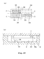
- Fig. 18 schematically shows the configuration of one example of a semiconductor device obtained by a manufacturing method according to the present invention, wherein Fig. 18(a) is a cross-sectional side view of the semiconductor device and Fig. 18(b) is a perspective view thereof;
- Fig. 19 is a plan view schematically illustrating the configuration of a lead frame used for manufacture of the semiconductor device shown in Fig. 18;
- Fig. 20 shows a fourth embodiment of a plastic molded type semiconductor device of the present invention, wherein Fig. 20(a) is a cross-sectional side view schematically showing the configuration of the fourth embodiment, and Fig. 20(b) is a perspective view of the fourth embodiment;
- Fig. 21 illustrates the fourth embodiment shown in Fig. 20, wherein Fig. 21(a) is a top view schematically showing the configuration of the fourth embodiment, and Fig. 21(b) is a cross-sectional view taken along line A - A' in Fig. 21(a);
- Fig. 22 is a view for describing a fifth embodiment of a plastic molded type semiconductor device of the present invention;
- Fig. 23 illustrates a lead frame employed in the fifth embodiment shown in Fig. 22, wherein Figs. 23(a) and 23(c) are respectively top views schematically showing the configuration of the lead frame, and Figs. 23(b) and 23(d) are respectively cross-sectional views of Figs. 23(a) and 23(c);
- Fig. 24 illustrates a sixth embodiment of a plastic molded type semiconductor device of the present invention, wherein Figs. 24(a) and 24(b) are respectively cross-sectional side views schematically showing the configuration of the sixth embodiment, and Fig. 24(c) is a cross-sectional view taken along line C - C' in Fig. 24(a); and
- Fig. 25 schematically shows the configuration of one example of a conventional plastic molded type semiconductor device, wherein Fig. 25(a) is a cross-sectional side view of the semiconductor device, and Fig. 25(b) is a perspective view thereof.
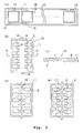
- Figs. 1(a) and 1(b) respectively show a first embodiment of the present invention. In these drawings, the same elements of structure as those shown in Figs. 25(a) and 25(b) are identified by the same reference numerals (the drawings illustrative of a second embodiment and embodiments subsequent thereto, which will be described below, are also similar to the above).
- Referring to Figs. 1(a) and 1(b),
reference numeral 10 indicates a resin or plastic molded type semiconductor device (hereinafter abbreviated as "semiconductor device"). As shown in Fig. 1(a), thesemiconductor device 10 comprises a rectangular and plate-shaped semiconductor element 2, a plurality ofleads 6 electrically connected to acircuit forming surface 2a of thesemiconductor element 2, a plurality of gold lines orwires 5 for respectively electrically connecting thesemiconductor element 2 and theleads 6 to each other on thecircuit forming surface 2a, and an insulatingadhesive tape 3 provided between theleads 6 and thesemiconductor element 2 so as to fix theleads 6 to thesemiconductor element 2. - The
leads 6 are disposed over thecircuit forming surface 2a of thesemiconductor element 2 and provided not so as to extend toward the sides of thecircuit forming surface 2a. Further, theleads 6 are respectively subjected to downset processing so as to be formed with differences in level by the thickness of theadhesive tape 3. Alower portion 6a of eachlead 6 is brought into contact with thesemiconductor element 2, whereas anupper portion 6b thereof is bonded and fixed onto thesemiconductor element 2 with theadhesive tape 3 interposed therebetween. As shown in Fig. 1(b), theseleads 6 are provided over thesemiconductor element 2 in two rows. Incidentally, thegold wires 5 for respectively electrically connecting theleads 6 and thesemiconductor element 2 to one another are electrically connected to their corresponding upper surfaces of thelower portions 6a of theleads 6 and are disposed not so as to extend out upwardly from the upper surfaces of theupper portions 6b of theleads 6. - The
adhesive tape 3 is composed of, for example, a polyimide resin and has unillustrated adhesive layers formed on both surfaces thereof. Further, theadhesive tape 3 is shaped in the form of a rectangular frame and bonded onto thecircuit forming surface 2a in a state in which its outer peripheral edge has substantially matched with its corresponding outer shape of thecircuit forming surface 2a. - Further, a
dambar 11 is fixed onto thecircuit forming surface 2a of thesemiconductor element 2 by theadhesive tape 3. Thedambar 11 has an outer shape substantially identical to the outer shape of thecircuit forming surface 2a and is formed in the same thickness as that of eachlead 6. Moreover, thedambar 11 is provided not so as to make contact with theleads 6 and disposed so that its outer edge substantially coincides with the outer edge of thecircuit forming surface 2a. - A
mold resin 7 is charged and hardened inside thedambar 11 on thecircuit forming surface 2a of thesemiconductor element 2. Thus, thecircuit forming surface 2a is sealed by themold resin 7 in a state in which the upper surface of thedambar 11 and the upper surfaces of theupper portions 6a of theleads 6 have been exposed. In thesemiconductor device 10, thesemiconductor element 2 thereof has surfaces other than thecircuit forming surface 2a, which have been exposed under the aforementioned resin sealing of thecircuit forming surface 2a by the mold resin. - A method of manufacturing the
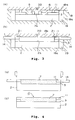
semiconductor device 10 will next be described. - A
lead frame 12 shown in Fig. 2(a) is first prepared. Thelead frame 12 comprises a metallead frame member 13 shaped in the form of a rectangular frame, and a plurality oflead frame bodies 15 connected to the inside of thelead frame member 13 through metal dambar supports 14. As shown in Figs. 2(b) and 2(c), thelead frame bodies 15 are respectively formed ofmetal dambars 11 shaped in the form of rectangular frames, which are connected to one another through the dambar supports 14, a plurality of metal leads 6 disposed within eachdambar 11 without contacting thedambar 11, and anadhesive tape 3 for coupling theseleads 6 to thedambars 11. - In order to fabricate each
lead frame body 15, as the lead frame body, one is first prepared as shown in Fig. 2(d), which comprises adambar 11, alead support 16 connected to thedambar 11, and leads 6 respectively coupled to both sides of thelead support 16. Next, the connecting sides of theleads 6, i.e., the ends thereof on thelead support 16 side are given metal plating 17 as shown in Fig. 2(e). Further, theadhesive tape 3 is placed on the surfaces of theleads 6, which are opposite to the surfaces thereof provided with themetal plating 17. Theadhesive tape 3 is a frame-shaped one having an outer shape substantially identical to that of thedambar 11. Further, as theadhesive tape 3, one is used which covers the entire back (corresponding to the same surface as the surface on the side opposite to each metal plating 17 applied to each lead 6) of thedambar 11 and has shapes and dimensions required to couple thedambar 11 and theleads 6 to one another. In regard to the portions stuck on theleads 6, however, the size of theadhesive tape 3 is adjusted so that theadhesive tape 3 is bonded only onto the back of eachlead 6 on the side uncoated with themetal plating 17. - After the
dambar 11 and theleads 6 have been coupled to each other by theadhesive tape 3, the downset processing is applied to the side of each lead 6 to which noadhesive tape 3 is bonded. Further, thelead support 16 is separated from thedambar 11 and theleads 6 to obtain thelead frame body 15 shown in Figs. 2(b) and 2(c). - Next, the
lead frame 12, which has been prepared in this way, is placed on thesemiconductor element 2 in such a manner that the outer edge of thedambar 11 of thelead frame body 15 substantially coincides with the outer edge of the circuit forming surface of thesemiconductor element 2. Further, theleads 6 and thedambar 11 are fixed onto thesemiconductor element 2 with theadhesive tape 3 by thermo compression bonding. - Next, the
leads 6 fixed onto thesemiconductor element 2 and thesemiconductor element 2 are connected to each other by themetal wires 5, followed by introduction into acavity 19 defined in amold 18 as shown in Figs. 3(a) and 3(b). Incidentally, Fig. 3(a) shows the side of thesemiconductor device 10 as seen in the direction indicated by arrow A in Fig. 1(b). Fig. 3(b) illustrates the side of thesemiconductor device 10 as seen in the direction indicated by arrow B in Fig. 1(b). - As the
mold 18, one is used in which the depth of thecavity 19 defined in a cavity-retainer plate orlower form 18a is equal to the total thickness of thesemiconductor element 2,adhesive tape 3 anddambar 11. Thus, themold 18 is held within thecavity 19 in a state in which the bottom face (corresponding to the surface opposite to the circuit forming surface) of thesemiconductor element 2 and the upper surfaces of thedambar 11 and eachlead 6 are interposed between the bottom face and top face (corresponding to the lower surface of anupper form 18b) that form thecavity 19. Further, themold 18 has aresin injection hole 20 and degassing holes 21 (see Fig. 3(b)) defined in theupper form 18b thereof. Each of dambar supports 14 of thelead frame 12 is interposed between the degassinghole 21 and the upper surface of thelower form 18a. - A molding resin is charged into the
cavity 19 through theresin injection hole 20 using the above-describedmold 18 and hardened at molding temperatures ranging from about 170°C to 180°C. At this time, the central portion of thecircuit forming surface 2a of thesemiconductor element 2 is filled with the resin as shown in Fig. 3(a). In doing so, thedambar 11 is shaped in frame form and the upper surface of thedambar 11 is brought into contact with theupper form 18b. Therefore, the filled resin is dammed by the dambar 11 and is hence overflowed toward the outside thereof. As a result, no resin flows into the side and bottom face of thesemiconductor element 2. Owing to the discharge of air in thecavity 19 from the degassing holes 21 during the resin filling, the molding resin is smoothly charged into thecavity 19. Thus, as shown in Fig. 1(b), the above-described resin charging allows only the upper surface of thedambar 11 and the upper surfaces of theupper sides 6b of theleads 6 to be exposed and permits thecircuit forming surface 2a other than those to be sealed. Further, thesemiconductor element 2 can be sealed with the molding resin in a state in which other surfaces except for thecircuit forming surface 2a are exposed. - Thereafter, the
semiconductor element 2 sealed with the molding resin is taken out from themold 18. Further, the dambar supports 14 each coupled to thedambar 11 are cut as shown in Fig. 4(a) and thedambar 11 is separated from thelead frame member 13 as shown in Fig. 4(b) thereby to obtain asemiconductor device 10. - Since the
molding resin 7 seals thecircuit forming surface 2a alone without covering the upper surfaces of theleads 6 and allows the surfaces other than thecircuit forming surface 2a to be exposed, the entire thickness of the thus-obtainedsemiconductor device 10 reaches a thickness obtained by simply adding the thicknesses of theadhesive tape 3 and the dambar 11 (or each lead 6) to the thickness of thesemiconductor element 2, thus resulting in a sufficient thin thickness. Further, since theleads 6 are disposed on and inside thecircuit forming surface 2a of thesemiconductor element 2, the implementation or packing area of thesemiconductor device 10 substantially coincides with the bottom area of thesemiconductor element 2. As a result, its substantial packing area becomes much smaller than ever. Thus, since thesemiconductor device 10 is so thin in thickness and very small in packing area, it can be more densely packaged or implemented on a printed board. - According to the method of manufacturing the
semiconductor device 10, since thelead frame body 15 composed of thedambar 11 identical in outer configuration or shape to thesemiconductor element 2 and theleads 6 connected to thedambar 11 via theadhesive tape 3 without causing electrical conduction, is used, the molding resin can be charged into thecavity 19 so that the flow of the molding resin is dammed by thedambar 11, thereby making it possible to easily manufacture thesemiconductor device 10. - Further, the upper surface of the
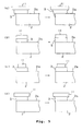
dambar 11 and the bottom face of thesemiconductor element 2 are interposed between the lower surface of theupper form 18b and the bottom face of thecavity 19 of thelower form 18a, and the resin is charged into thecavity 19 in this condition. Thus, since the charged resin is dammed by thedambar 11, thecavity 19 is not subjected to other restrictions if its size extending in the plane direction is larger than that of thesemiconductor element 2. Accordingly, even if semiconductor elements different in size from each other are used, themold 18 can be shared between the semiconductor elements if their thicknesses are identical to each other. - Fig. 5(a) is a view for explaining a first modification of the manufacturing method described by reference to Figs. 2 through 4. The first modification will be described with reference to Fig. 5(a).
- The first modification is different from the manufacturing method shown in Figs. 2 through 4 in that each lead frame body of a lead frame to be used slightly differs from the above-described
lead frame body 15. - Namely, as the lead frame body employed in the first modification, one is used in which as shown in Fig. 5(a), the outside dimension of an
adhesive tape 3 is formed so as to be slightly larger than that of acircuit forming surface 2a of asemiconductor element 2 and the outside diameter of adambar 11 is formed so as to be slightly larger than that of theadhesive tape 3. - Using such a lead frame body, the
adhesive tape 3 is bonded to thecircuit forming surface 2a in the same manner as the above embodiment in such a manner that the outer edge of theadhesive tape 3 substantially coincides with the outer edge of thecircuit forming surface 2a. Subsequently, respective process steps are executed in the same manner as the above-described embodiment. - Thus, when the
adhesive tape 3 is bonded onto thecircuit forming surface 2a by thermo compression bonding, the outer edge of theadhesive tape 3 is partly melted upon thermo compression bonding as shown in Fig. 5(a). As a result, the melted portion exudes or oozes so as to cover a portion of the side of thesemiconductor element 2 as well as to cover even a portion of the outer edge of the lower surface of thedambar 11. - Thus, according to the above-described manufacturing method, the resultant semiconductor device (not shown) is constructed in such a manner that the
adhesive tape 3 is bonded to the lower surface of thedambar 11 in a wider area at the side portion of the semiconductor device and theadhesive tape 3 is also bonded to thesemiconductor element 2 so as to extend to a side upper portion thereof as well as to thecircuit forming surface 2a. It is thus possible to prevent impurities from externally entering the surface of thesemiconductor element 2. - The state of the
adhesive tape 3 subjected to the thermo compression bonding, of thesemiconductor device 10 obtained by the manufacturing method shown in Figs. 2 through 4 will be described for reference purposes with reference to Fig. 5(b). Since anadhesive tape 3 and adambar 11 are both substantially identical in size to acircuit element surface 2a of asemiconductor element 2 in the present example, the oozing of theadhesive tape 3 due to its melting is less provided so that the area for covering the side of thesemiconductor element 2 is only slight. - If an
adhesive tape 3 is substantially identical in size to acircuit element surface 2a and adambar 11 is smaller than thecircuit element surface 2a as shown in Fig. 5(c), then the oozing of theadhesive tape 3 due to its melting occurs in the direction in which theadhesive tape 3 covers the side of thedambar 11. - If an
adhesive tape 3 is substantially identical in size to acircuit element surface 2a and adambar 11 is larger than thecircuit element surface 2a as shown in Fig. 5(d), then the oozing of theadhesive tape 3 due to its melting occurs in the direction in which theadhesive tape 3 covers the side of thesemiconductor element 2 and the lower surface of thedambar 11. However, since theadhesive tape 3 is substantially identical in size to thecircuit element surface 2a, the amount of oozing of theadhesive tape 3 due to its melting becomes smaller than that in Fig. 5(a). - Figs. 6(a) and 6(b) are respectively views for describing a second modification of the manufacturing method described with reference to Figs. 2 through 4. The second modification will be described with reference to Figs. 6(a) and 6(b).
- The second modification is different principally from the manufacturing method shown in Figs. 2 through 4 in that each of
grooves 22 used for degassing upon resin filling and hardening is defined in adambar support 14 and adambar 11 of alead frame 12 to be used. - Namely, as the
lead frame 12 employed in the second modification, one is prepared in which as shown in Fig. 6(a), thegroove 22 extending from the inner edge of thedambar 11 to the outer edge of alead frame member 13 through thedambar support 14 is formed as shown in Fig. 6(a). Thegroove 22 serves as a hole used for degassing upon resin filling and hardening as will be described later. Further, thegroove 22 is defined in thelead frame 12 so as to be located on the side opposite to the side of bonding of theadhesive tape 3. - In order to fabricate a semiconductor device, using the
lead frame 12 havingsuch grooves 22 define therein, anupper form 23 different from theupper form 18b of themold 18 shown in Fig. 3(b) and having no degassinggrooves 21 can be used as illustrated in Fig. 6(b). Namely, thelead frame 12 having thegrooves 22 defined therein is used and provided so that eachgroove 22 extends from within acavity 19 to the outside of theupper form 23. Owing to the provision of thelead frame 12, air in thecavity 19 is discharged through thegrooves 22 upon resin filling, whereby amolding resin 7 can be smoothly charged into thecavity 19. - Thus, according to the manufacturing method, the
upper form 23 used for the sealing of the molding resin can eliminate the need for its processing except for the provision of theresin injection hole 20. Accordingly, the manufacturing cost can be reduced and theupper form 23 can be made full of the sharing that less limitations are placed on the size of thesemiconductor element 2. - Figs. 7(a) and 7(b) are respectively views for describing a third modification of the manufacturing method described with reference to Figs. 2 through 4. The third modification will be described with reference to Figs. 7(a) and 7(b).
- The third modification is different principally from the second modification shown in Figs. 6(a) and 6(b) in that as a
lead frame 12, one is used in whichgrooves 22 are defined in adambar support 14, a dambar-to-dambar lead 24 is provided betweenlead frame bodies groove 25 and ahole 26 serving as degassing holes are defined in the dambar-to-dambar lead 24 as shown in Fig. 7(a). - Namely, as the
lead frame 12 employed in the third modification as shown in Fig. 7(a), one is prepared in which thegrooves 25 each extending from the inner edge of onedambar 11 to the inner edge of theother dambar 11 through the dambar-to-dambar lead 24 are defined in thelead frame bodies adhesive tape 3, and eachhole 26 extending through the bonding surface of theadhesive tape 3 from thegroove 25 is defined in the dambar-to-dambar lead 24. - In order to fabricate a semiconductor device, using the
lead frame 12 having thegrooves hole 26 defined therein, amold 27 is used in which as shown in Fig. 7(b), thedegassing grooves 21 are not provided in the same manner as theupper form 23 of the mold shown in Fig. 6(b) and resin sealing is simultaneously performed on a plurality of semiconductor elements, using a wide cavity. Namely, themold 27 has an upper form 27b having a plurality of resin injection holes 20 defined therein. A resin is simultaneously injected through the resin injection holes 20 as shown in Fig. 7(b) upon resin filling. - When the resin is injected in this way, air inside the
dambar 11 is squeezed out by the resin and some is discharged outside themold 27 through thegrooves 22. Simultaneously, the remaining air passes through thegrooves 25 and flows between thesemiconductor elements hole 26 being in communication with eachgroove 25. Accordingly, the manufacturing method can also provide smooth filling of themolding resin 7. Further, the manufacturing method is also superior to the manufacturing method shown in Figs. 6(a) and 6(b) in that since air flows between the dambars 11 and 11, air bleeding or ventilation can be made smoother and a reduction in resin filling characteristic can be sufficiently suppressed owing to the formation of the path for discharging air from the inside of thedambar 11 to the outside of eachsemiconductor element 2 even if the efficiency of air extraction or ventilation is reduced due to a complex configuration of thelead frame 12. Further, the plurality ofsemiconductor elements 2 can be resin-sealed simultaneously by onemold 27 and hence the fabrication cost of the mold can be made cheap and the manufacturing cost thereof can be reduced. - Fig. 8(a) is a view for describing a fourth modification of the manufacturing method described with reference to Figs. 2 through 4.
- The fourth modification is different from the manufacturing method shown in Figs. 2 through 4 in that as a mold to be used, one is used in which grooves are defined in the bottom face for forming a cavity thereof.
- Namely, for example, the manufacturing method shown in Figs. 2 through 4 has a problem in that when a
foreign material 28 exists within acavity 19 as shown in Fig. 8(b), theforeign material 28 will cause damage to asemiconductor element 2 because thesemiconductor element 2 and thelead frame 12 placed thereon are interposed between the bottom face for forming thecavity 19, of thelower form 18a of themold 18 shown in Fig. 3(a) and the lower surface of theupper form 18b thereof. Particularly when its damage is serious, cracks 29 are produced, so that a function used as for the semiconductor device is impaired. - Thus, in the fourth modification,
grooves 30 are defined in the bottom face of thelower form 18a, for forming thecavity 19 as shown in Fig. 8(a) to reduce the probability that eachsemiconductor element 2 will be damaged by theforeign material 28, even if theforeign material 28 exists. The formation of thegrooves 30 in the bottom face has no effect on thesemiconductor element 2 and can provide smooth resin filling if theforeign material 28 falls within the correspondinggroove 30 even if theforeign material 28 remains within thecavity 19 upon resin filling. - In the fourth embodiment, the
grooves 30 are defined in the bottom face of thecavity 19. However, even if simple recesses or concave portions are defined in place of the grooves, the influence of theforeign material 28 can be made small. - Fig. 9(a) is a view for describing a fifth modification of the manufacturing method described with reference to Figs. 2 through 4.
- The fifth modification is different from the fourth embodiment in that the bottom face of each groove defined in the bottom face of a
cavity 19 is formed by a downwardly-expanded curved surface. - Namely, in the fifth modification,
grooves 31 defined in the bottom face of thecavity 19 are shaped in the form of semicircles as seen in the transverse cross-section as shown in Fig. 9(a) and hence the bottom faces thereof are formed as curved surfaces expanded downwards in the form of the semicircles. - In the fourth modification, a
foreign material 28 is considered to remain within each ofgrooves 30 judging from the shape of thegroove 30 even if air is blown against theforeign material 28 by an air gun, for example so as to blow theforeign material 28 off with a view toward removing theforeign material 28 as shown in Fig. 9(b). In the fifth modification, however, theforeign material 28 can be easily removed because eachgroove 31 has the curved shape. Thus, the time required to remove the foreign materials is shortened and correspondingly the time necessary for the execution of process steps can be reduced. Further, the occurrence of damage in thesemiconductor element 2 by the foreign materials can be curbed. - In the fifth modification, the
grooves 31 have been defined in the bottom face of thecavity 19. However, concave portions may be simply defined in place of the grooves in the same manner as the fourth modification. If the concave portions have concave surfaces respectively formed by curved surfaces expanded downwardly of the bottom face of thecavity 19 in this case, then the influence of theforeign materials 28 can be reduced. - Fig. 10(a) is a view for describing a sixth modification of the manufacturing method described with reference to Figs. 2 through 4.
- The sixth modification is different from the fourth modification in that grooves or concave portions defined in the bottom face of a
cavity 19 are respectively symmetrically formed or disposed in their upward and downward directions and their right and left directions in terms of the shape of the bottom face as seen in the plane thereof. - Namely, in the sixth modification as shown in Fig. 10(a), concave portions or grooves indicated by C, D, E and F in Fig. 10(a) are defined in the bottom face 19a of the
cavity 19. Here, C, D, E and F respectively indicate further first, second, third and fourth examples of the sixth modification. In the examples, the illustration of the entire bottom faces 19a thereof is omitted and only parts of the faces divided into four are illustrated. - The structure indicated by C in Fig. 10(a) is one in which
concave portions 32 circular as seen in the plane are formed and arranged at equal intervals in the vertical and horizontal directions. The structure indicated by D in Fig. 10(a) is one in which a plurality ofgrooves 33 extending in the horizontal direction as seen in the drawing are formed and arranged in parallel and at equal intervals. Further, the structure indicated by E in Fig. 10(a) is one in which a plurality ofgrooves 34 extending in the vertical direction as seen in the drawing are formed and arranged in parallel and at equal intervals. The structure indicated by F in Fig. 10(a) is one in which a plurality ofgrooves 35 rectangular and frame-shaped as seen in the plane are formed and arranged concentrically and at equal intervals. - Meanwhile, the fourth modification has a possibility that when the
semiconductor element 2 is placed within the mold and clamped where thegrooves 30 are asymmetrically disposed as seen in the plane as shown in Fig. 10(b), the back of thesemiconductor element 2 will strike against the corner of eachgroove 30 if thesemiconductor element 2 has a slight inclination, whereby the force is concentrated on the corner thereof to thereby produce cracks 36. - However, since the grooves defined in the mold, which make contact with the back of the
semiconductor element 2, are arranged symmetrically with respect to the back of thesemiconductor element 2 in the case of the vertically and horizontally-symmetrical structures as indicated by C, D, E and F, the bottom surface of thecavity 19 is uniformly brought into contact with the back of thesemiconductor element 2 upon placement of thesemiconductor element 2 within the mold. Thus, no inclination is produced in thesemiconductor element 2 and no damage occurs in the back of thesemiconductor element 2 upon its clamping. - Even in the case of the sixth modification, the concave surfaces of the
grooves cavity 19 may be formed by curved surfaces expanded downwardly of the bottom face of thecavity 19. - Figs. 11(a) and 11(b) are respectively views for describing a seventh modification of the manufacturing method described with reference to Figs. 2 through 4. Incidentally, Figs. 11(a) and 11(b) respectively illustrate a state of the present modification after a lead frame has been provided on a
semiconductor element 2 and a resin has been charged. - The seventh modification is different principally from the manufacturing method shown in Figs. 2 through 4 in that portions thinner than a dambar in thickness are respectively provided at dambar supports of a lead frame to be used.
- Namely, in the seventh modification as shown in Figs. 11(a) and 11(b), a
used lead frame 36 is different from thelead frame 12 shown in Fig. 7(a) by way of example and thin-walled portions 14a are attached to their corresponding dambar supports 14. Each thin-walled portion 14a is provided at a portion provided in continuous with thedambar 11. Eachdambar support 14 corresponding to a portion continuously connected to the thin-walled portion 14a is formed in the same thickness as that of thedambar 11. - Since the thin-
walled portion 14a is attached to eachdambar support 14 in the above-described manner, eachdambar support 14 is easy to cut at the thin-walled portion 14a as a matter of course, so that alead frame body 15 becomes easy to be detached from alead frame member 13. Thus, in the seventh modification, thelead frame 36 has dambar-to-dambar leads 37 each formed between the dambars 11 and 11 existing between thelead frame bodies lead frame body 15 from being unexpectedly detached from thelead frame member 13 as described above. Even in the case of the dambar-to-dambar lead 37, thin-walled portions dambars 11 so as to make it easy to cut the dambar-to-dambar lead 37. - After the completion of the resin filling as shown in Figs. 11(a) and 11(b), the unnecessary dambar supports 14 are cut as shown in Fig. 4(a) to divide semiconductor devices into pieces as the final process step. At this time, there is a fear of the occurrence of
cracks 38 in themolding resin 7 as illustrated in Fig. 11(c). This will be considered to occur due to the fact that eachdambar support 14 is hard to be cut when it is formed thick in thickness. - However, since the thin-
walled portions 14a are respectively attached to the dambar supports 14 as shown in Figs. 11(a) and 11(b), the seventh modification allows the prevention of occurrence of thecracks 38 referred to above owing to the cutting of the thin-walled portions 14a. Further, since the thin-walled portions dambar lead 37 in the same manner as described above, the dambar-to-dambar lead 37 is easy to be cut, whereby thecracks 38 is prevented from occurring even when the dambar-to-dambar lead 37 is cut. - Figs. 12(a) and 12(b) are respectively views for explaining an eighth modification of the manufacturing method described with reference to Figs. 2 through 4. Incidentally, Figs. 12(a) and 12(b) respectively illustrate a state of the present modification after a lead frame has been provided on a
semiconductor element 2 and a resin has been charged. - The eighth modification is different from the seventh modification shown in Figs. 11(a) and 11(b) in that as a lead frame to be used, one is used in which adhesive tapes are provided in place of the thin-
walled portion 14a of eachdambar support 14 and the dambar-to-dambar lead 37. - Namely, in the eighth modification, the
lead frame 40 used as shown in Figs. 12(a) and 12(b) is one having a structure in which dambar supports 41 extending outwardly fromdambars 11 oflead frame bodies 15 are respectively provided at intervals away from thedambars 11 and connected thereto through anadhesive tape 3a. Even in the case of thelead frame 40, thelead frame bodies lead frame bodies 15 and alead frame member 13. Here, theadhesive tapes 3a and 3b are ones formed by extending theadhesive tape 3 for coupling thedambar 11 and theleads 6 to each other by required portions in advance. - Thus, according to the eighth modification, the thin and soft
adhesive tapes 3a and 3b are cut when the dambar supports 41 are cut and the dambars 11 and 11 are cut away from each other in order to divide semiconductor devices into pieces after the completion of resin filling. As a result, the degree of an under-cutting load on amolding resin 7 can be extremely reduced, thereby making it possible to reliably prevent thecracks 38 shown in Fig. 11(c) from occurring. When the thin-walled portions 14a of the dambar supports 14 and the thin-wall portions 37a of the dambar-to-dambar leads 37 are cut, some of the thin-walled portions adhesive tapes 3a and 3b in the eighth modification shown in Figs. 12(a) and 12(b), problems are little offered outwardly even if the portions left behind by cutting appear. Further, there is no possibility that the portions will interfere with the implementation of the adjacent semiconductor device on the printed board even in the case of the implementation of each semiconductor device on the printed board. - Fig. 13(a) is a view showing a modification of the first embodiment shown in Figs. 1(a) and 1(b).
Reference numeral 42 in Fig. 13(a) indicates a semiconductor device. - The
semiconductor device 42 is different from thesemiconductor device 10 shown in Figs. 1(a) and 1(b) in that adambar 43 is formed much thicker than each of leads 6 in thickness. - In order to fabricate the
semiconductor device 42, as alead frame 12, one provided with thedambar 43 thicker than each lead 6 in thickness is prepared and may be processed subsequently in a manner similar to the manufacturing method shown in Figs. 2 through 4. However, a mold to be used is different from themold 18 shown in Fig. 3(a) in that as shown in Fig. 13(b), the depth of acavity 45 defined in a lower form 44a is deeper than that of thecavity 19 defined in themold 18 shown in Fig. 3(a) by the difference between the thicknesses of thedambar 43 and thelead 6 and aprojection 46 that protrudes by the difference between the thicknesses of thedambar 43 and thelead 6, is provided in the center of a lower surface of anupper form 44b. - When the
semiconductor device 10 shown in Figs. 1(a) and 1(b) is implemented on a printed board, eachlead 6 is electrically connected and fixed to a printedboard 48 bysolder 47 as shown in Fig. 13(c). However, since the entire configuration of thesemiconductor device 10 is virtually made up of thesemiconductor element 2, the thermal expansion coefficient thereof substantially coincides with about 3 x 10⁻⁶/°C corresponding to a thermal expansion coefficient of silicon. On the other hand, the thermal expansion coefficient of the printedboard 48 is substantially identical to 2 to 3 x 10⁻⁵/°C corresponding to a thermal expansion coefficient of a resin. Thus, the thermal expansion coefficient of the printedboard 48 is increased by one digit as compared with thesemiconductor device 10. - However, since the thermal expansion coefficient of the printed
board 48 is larger than that of thesemiconductor device 10 in this way, a thermal stress produced due to the difference between the thermal expansion coefficients is concentrated on thesolder 47 used as each junction between the printedboard 48 and thesemiconductor device 10 after the implementation of thesemiconductor device 10 on the printedboard 48. When the thermal stress increases, cracks are produced in the solder, so that there is a fear that they will result in a conductive failure. In order to prevent its occurrence, for example, a substrate composed of ceramic whose thermal expansion coefficient is close to that of thesemiconductor element 2, may be used in place of the printedboard 48. However, since the ceramic substrate is so expensive in this case, a great increase in cost will be incurred. - Thus, in order to solve such inconvenience, the
semiconductor device 42 according to the present modification is constructed in such a manner that thedambar 43 is much thicker than each lead 6 in thickness as shown in Fig. 13(a). When thesemiconductor device 42 is implemented on the printedboard 48, grooves 49 corresponding to the positions and configurations of thedambars 43 are defined in predetermined positions on the printedboard 48 in advance. Thedambars 43 of thesemiconductor device 42 are respectively fitted in the grooves 49 of the printedboard 48 as projections and are connected and fixed to the printedboard 48 by thesolder 47 in this condition. - In doing so, the thermal stress produced due to the difference between the thermal expansion coefficients is reduced by fitting the projections composed of the
dambars 43 in their corresponding grooves 49 defined in the printedboard 48, whereby cracks can be prevented from occurring in thesolder 47. - Thus, when the
semiconductor device 42 according to the present modification is constructed as a structure in which thesemiconductor device 42 is implemented on the board, such a structure can prevent the cracks from occurring in thesolder 47 used for fixing thesemiconductor device 42. As a result, the electrical connections between the semiconductor device and the printed board by thesolder 47 can be kept satisfactory. - Fig. 14 is a view showing a second embodiment of the present invention.
Reference numeral 14 in Fig. 14 indicates a semiconductor device. - The
present semiconductor device 50 is different from thesemiconductor device 10 shown in Fig. 1(a) and 1(b) in that surfaces of asemiconductor element 2, which are other than acircuit forming surface 2a thereof are covered with a coating resin. - Namely, the
semiconductor device 50 shown in Fig. 14 is provided in such a manner that the surfaces of thesemiconductor element 2, other than thecircuit forming surface 2a and side end surfaces of anadhesive tape 3 placed on thecircuit forming surface 2a are covered with acoating resin 51. Thecoating resin 51 is composed of, for example, an epoxy resin, a polyimide resin or the like and ranges from about 20µm to 30µm in thickness. Thecoating resin 51 is one coated so as to keep the size of thesemiconductor device 50 itself almost constant. - In order to fabricate the
semiconductor device 50, a process up to mold resin sealing is executed in a manner similar to the manufacturing method shown in Figs. 2 through 4. Thereafter, the resultant semiconductor device subjected to the resin sealing is immersed into aresin tank 52 fully filled with a liquid resin 51a obtained by dissolving thecoating resin 51 in a solvent, as shown in Fig. 15(a). At this time, the resin-sealed semiconductor device is kept in a state in which eachdambar support 14 of alead frame 12 is not being cut. The size of an opening of theresin tank 52 is set to a size in which the dambar supports 14 are suspended at the edges of theresin tank 52 when the semiconductor device is immersed into theresin tank 52. In this condition, thesemiconductor element 2 side is immersed into the liquid resin 51a for a suitable time interval as mentioned above in the state in which the dambar supports 14 of the semiconductor device have been suspended at the edges of theresin tank 52. Next, the semiconductor device is pulled up from theresin tank 52 and the coating resin attached to the semiconductor device is dried and hardened at a temperature of about 100°C for several hours as shown in Fig. 15(b). Thereafter, the dambar supports 14 are cut in a manner similar to the manufacturing method shown in Figs. 2 through 4 to thereby obtain thesemiconductor device 50 shown in Fig. 14. - In the
semiconductor device 50 obtained in this way, the covering of the surfaces of thesemiconductor element 2, other than thecircuit forming surface 2a with thecoating resin 51 makes it hard to scratch the surfaces upon handling of thesemiconductor device 50, for example and improve the resistance of thesemiconductor device 50 to an impact. Namely, since thesemiconductor element 2 is composed of a brittle material such as silicon or the like, large cracks are produced even if any flaws occur in the surfaces, so that the function of thesemiconductor element 2 is apt to be impaired. However, the covering of the surfaces with thecoating resin 51 can reduce an external impact so as to prevent the occurrence of the cracks. Further, since the boundary between thecircuit forming surface 2a of thesemiconductor element 2a and the back of theadhesive tape 3 is also covered with thecoating resin 51 as shown in Fig. 14, the resistance of the semiconductor device to moisture can be also improved. - According to the method of manufacturing the
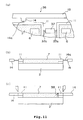
semiconductor device 50, since the dambar supports 14 are suspended at the edges of theresin tank 52 fully filled with the liquid resin 51a and the lower side of eachdambar support 14 is immersed into the liquid resin 51a before the cutting of the dambar supports 14, resin coating is extremely easy and the fabrication of thesemiconductor device 50 does not need a special device. Further, thesemiconductor device 50 can be fabricated easily and in full correspondence with its mass productivity. - Fig. 16(a) is a view illustrating a third embodiment of the present invention.
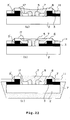
Reference numeral 53 in Fig. 16(a) indicates a semiconductor device. - The
semiconductor device 53 is different from thesemiconductor device 10 shown in Figs. 1(a) and 1(b) in that nodambar 14 is provided. - Namely, the
semiconductor device 53 shown in Fig. 16(a) comprises leads 6 provided on acircuit forming surface 2a of asemiconductor element 2 with anadhesive tape 3 interposed therebetween, andgold wires 5 for respectively electrically connecting theseleads 6 to thesemiconductor element 2. Further, thesemiconductor device 53 is constructed such that theleads 6 and thegold wires 5 are sealed with amold resin 7 in a state in which the upper surfaces of theleads 6 have been exposed. - In order to fabricate the
semiconductor device 53, alead frame 54 shown in Fig. 17(a) is first prepared. Thelead frame 54 is one in whichadhesive tapes 55 each having arectangular opening 55a are bonded to alead frame member 13 and parts ofleads 6 are bonded and fixed to theadhesive tapes 55. Each lead frame body (not shown) is composed of theadhesive tape 55 and the leads. In theadhesive tape 55, the shape of eachopening 55a defined therein is smaller than the outer shape of acircuit forming surface 2a of asemiconductor element 2. Further, the parts of theleads 6 are bonded to the inner edge of eachopening 55a and the remaining parts thereof extend into theopening 55a. - Here, the
adhesive tape 55 is constructed as shown in Fig. 17(c). Namely, anadhesive layer 56a is formed on the surface of theadhesive tape 55 on the side of the bonding of each lead 6 to theadhesive tape 55 so as to extend from the inner edge thereof for defining theopening 55a to the position of bonding of each lead 6 to theadhesive tape 55. Further, anadhesive layer 56b is formed on the opposed surface of theadhesive tape 55 so as to extend from the inner edge thereof for defining theopening 55a to the position identical to that of the outer edge of thecircuit forming surface 2a of thesemiconductor element 2. Moreover, an adhesive layer (resin is not shown) is provided at the position of the surface of theadhesive tape 55 on the side of bonding of each lead 6 to the surface thereof, which position corresponds to thelead frame member 13, and no adhesive layer is formed at other locations. - Next, each lead frame body of the
lead frame 54 is placed on thesemiconductor element 2 in such a manner that the outer edge of theadhesive layer 56b on theadhesive tape 55 substantially coincide with the outer edge of thecircuit forming surface 2a of thesemiconductor element 2. Thereafter, theleads 6 are fixed onto thesemiconductor element 2 by theadhesive tape 55. - Next, the
leads 6 on thesemiconductor element 2 are respectively connected to thecircuit forming surface 2a of thesemiconductor element 2 by thegold wires 5. Further, thesemiconductor element 2 connected with thegold wires 5 is placed in acavity 58 defined in amold 57 as shown in Fig. 17(b). As themold 57, one is used in which a recess orconcave portion 58a having a depth equal to the thickness of thesemiconductor element 2 is defined in alower form 57a and an openconcave portion 58b being a size smaller than thecircuit forming surface 2a is defined in anupper form 57b. - The
mold 57 referred to above is used and a mold resin is charged into thecavity 58 through aresin injection hole 20 in a state in which the outer peripheral portion of theadhesive tape 55 is being interposed between thelower form 57a and theupper form 57b, followed by hardening of the charged resin. Thereafter, thesemiconductor element 2 is taken out from themold 57 to thereby obtain thesemiconductor element 2 in which resin sealing has been completed as shown in Fig. 17(c). Further, theadhesive tape 55 extending toward each side of thesemiconductor element 2 is cut to obtain thesemiconductor device 53 shown in Fig. 16(a). - Since no dambar is provided in the
semiconductor device 53 according to the present embodiment, electrical conduction between theleads solder 59 and each dambar will not occur when thesemiconductor device 53 is implemented on the printedboard 48, usingsolder 59 as shown in Fig. 16(c). Accordingly, an electrical failure in the above implemented state can be suppressed. - According to the method of manufacturing the
semiconductor device 53, since each adhesive layer is provided only at the predetermined position of theadhesive tape 55 for forming each lead frame body, theadhesive tape 55 can be prevented from being cemented to themold 57 even if the outer peripheral portion of theadhesive tape 55 is interposed between thelower form 57a andupper form 57b of themold 57 and the mold resin sealing is executed in this condition. Thus, since the resin sealing process can be performed without a hitch, thesemiconductor device 53 can be easily manufactured. - Figs. 18(a) and 18(b) are respectively views showing one example of a plastic molded type semiconductor device of the present invention, which is obtained by a method of manufacturing the semiconductor device.
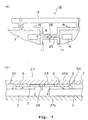
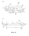
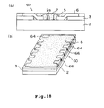
Reference numerals 60 in Figs. 18(a) and 18(b) indicate a semiconductor device. - The method of manufacturing the
semiconductor device 60 is different from the manufacturing method described with reference to Figs. 2 through 4 in that alead frame 61 shown in Fig. 19 is used. - The
lead frame 61 comprises alead frame member 13 and alead frame body 63 connected to the inside of thelead frame member 13 through a plurality of dambar supports 62. Thelead frame body 63 comprises a frame-shapeddambar 64 having an outer shape substantially identical to that of acircuit forming surface 2a of asemiconductor element 2, a plurality ofleads 6 extending inwardly of thedambar 64 in continuous or connection with thedambar 64, alead support 65 for connecting between theseleads dambar 64, and an adhesive tape (not shown) bonded to these so as to extend from one surface of thedambar 64 to the course or middle of eachlead 6. Eachresin portion 66 composed of an insulating resin is formed between all theadjacent leads dambar 64 so as to provide electrical discontinuity (non-conduction) between theseleads resin portion 66 is the same resin as a mold resin to be filled subsequently. Thelead frame 61 is different from thelead frame 12 shown in Figs. 2(a) through 2(e) in that theleads 6 are given metal plating (solder plating) after the completion of mold resin sealing as will be described later, without applying metal plating to theleads 6 in the state of the lead frame. - In order to fabricate the
semiconductor device 60, using such alead frame 61, thelead support 65 is eliminated from thelead frame body 63 in advance. Further, thelead frame body 63 of thelead frame 61 is placed on thecircuit forming surface 2a of thesemiconductor element 2 in the same manner as the case shown in Figs. 2 through 4 and fixed to thecircuit forming surface 2a with the adhesive tape. - Next, the
leads 6 on thesemiconductor element 2 and thecircuit forming surface 2a of thesemiconductor element 2 are electrically connected to each other withgold wires 5. Further, thesemiconductor element 2 connected with thegold wires 5 is introduced into a cavity of a mold (not shown). Moreover, the inside of thedambar 64 is filled with the mold resin within the mold to seal thecircuit forming surface 2a of thesemiconductor element 2. Thereafter, thesemiconductor element 2 is taken out from the mold and theleads 6 are given metal plating (solder plating). Further, the dambar supports 62 are cut so as to obtain thesemiconductor device 60 shown in Figs. 18(a) and 18(b). - Since the
dambar 64 has theresin portion 66, thesemiconductor device 60 obtained in this way can avoid electrical conduction between theadjacent leads leads 6 are continuously connected to thedambar 64. - According to the method of manufacturing the
semiconductor device 60, since theleads 6 are respectively electrically connected to the dambar supports 62 through thedambar 64, theleads 6 can be given solder plating by the use of the dambar supports 62 in the same manner as ever. - Figs. 20(a) and 20(b) are respectively views showing a fourth embodiment of the present invention.
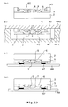
- In the present embodiment, a
dambar 11 is subjected to half etching at portions adjacent toleads 6 as shown in Figs. 20(a) and 20(b). The half-etched portions are covered with amold resin 7. - In a lead frame employed in the present embodiment, as illustrated in Figs. 21(a) and 21(b), a
dambar 11 is subjected to half etching 11' and supports 70 are formed adjacent to the half-etched portions. The supports 70 are used to prevent the half-etched portions 11' from extending out to end surfaces of thedambar 11 and thesupports 70. Thus, since only the dambar adjacent to theleads 6 is covered with the resin, the distance between each lead and thedambar 11 increases so that the occurrence of electrical leakage can be reduced. - Further, the half-etched portions are formed within the planes of both the
dambar 11 adjacent to the leads and thesupports 70 adjacent thereto. Thus, when upper and lower portions of the half-etched portions are held by an unillustrated mold and the resin is injected therein, the resin is introduced into the half-etched portions. Thereafter, the resin stops flowing at the end surfaces of thedambar 11 and thesupports 70. Thus, the neighborhood of eachlead 6 can be covered with the mold resin. - Figs. 22 (a) through 22(c) are respectively views showing applications of a fifth embodiment of the present invention. The provision of a steplike offset or a difference in level between a dambar 11 and each
lead 6 allows a reduction in electrical leakage produced between the dambar 11 and eachlead 6. - In these applications, insulating
tapes 3 and 3' are provided in double form at leads 6 alone as shown in Figs. 22(a) through 22(c). Owing to the configuration referred to above, the thickness of eachlead 6 becomes thicknesses of the twoinsulating tape 3 and 3' and the thickness of thedambar 11 is one insulatingtape 3 thick. Therefore, a difference in level corresponding to the insulating tape 3' can be formed between the dambar 11 and eachlead 6. - Fig. 23 is a view for describing a lead frame employed in each application shown in Fig. 22. Fig. 22(a) is a view showing the manner in which an adhesive tape 3' is bonded to each lead. Fig. 22(b) is a cross-section cut away at each lead in Fig. 22(a). Fig. 22(c) is a view illustrating the manner in which after the insulating tape 3' has been bonded to each lead, an insulating
tape 3 is further cemented thereto and eachlead 6 is subjected to bending. Fig. 22(d) is a cross-section cut away at the leads in Fig. 22(c). A difference in level corresponding to one insulating tape 3' is formed between the dambar 11 and eachlead 6 by forming each lead as shown in Fig. 22(d). - Figs. 24 (a) through 24(c) are respectively views showing a sixth embodiment of the present invention. In the embodiment shown in Fig. 24,
grooves 71 identical in height to adambar 11 are provided between respective adjacent leads 6. Fig. 24(a) is a cross-section cut away at the leads, Fig. 24(b) is a cross-section cut away at a resin portion, and Fig. 24(c) is a cross-sectional view taken along line C - C' in Fig. 24(a). - In the present embodiment, a difference in level, which corresponds to an insulating tape 3' is provided between the dambar 11 and each
lead 6. Further, thegrooves 71 identical in height to thedambar 11 are provided between theleads 6. Therefore, electrical leakage produced between theleads - While the present invention has been described with reference to the illustrative embodiments, this description is not intended to be construed in a limiting sense. Various modifications of the illustrative embodiments, as well as other embodiments of the invention, will be apparent to those skilled in the art on reference to this description. It is therefore contemplated that the appended claims will cover any such modifications or embodiments as fall within the true scope of the invention.
Claims (21)
- A plastic molded type semiconductor device comprising:a semiconductor element having electrodes provided on a surface thereof;a dambar formed along the outer periphery of the surface of said semiconductor element;a plurality of leads respectively electrically connected to said electrodes and provided inside said dambar electrically independent of said dambar; anda mold resin formed within a region surrounded by said dambar and formed so as to expose parts of said leads.
- A plastic molded type semiconductor device according to claim 1, wherein said dambar and said leads are secured to said semiconductor element by an insulating tape.
- A plastic molded type semiconductor device according to claim 1, wherein the thickness of said dambar is thicker than that of said each lead.
- A plastic molded type semiconductor device according to claim 1, wherein the side and back of said semiconductor element are covered with a coating resin.
- A plastic molded type semiconductor device comprising:a semiconductor element having electrodes provided on a surface thereof;an adhesive tape formed on the surface of said semiconductor element in a state in which the electrodes are being exposed;a plurality of leads fixed onto said adhesive tape and extending to the neighborhoods of said electrodes through portions thereof bent in the direction of the electrodes;conductive wires for respectively electrically connecting said leads and the electrodes; anda mold resin for sealing parts of said leads, said electrodes and said conductive wires so that portions of said leads, each corresponding to a portion on said adhesive tape, are exposed.
- A method of manufacturing a plastic molded type semiconductor device, comprising the following steps:a step for preparing semiconductor elements each having electrodes provided on a surface thereof;a step for forming a lead frame having frame-shaped dambars each having an outer shape substantially identical to that of the surface of said each semiconductor element and a plurality of leads disposed within said each dambar electrically independent of said dambar, said dambar and said leads being fixed to each other with an insulating adhesive tape;a step for placing said lead frame on the surface of said each semiconductor element so that said dambar substantially coincides in outer edge with the surface of said semiconductor element and fixing said leads and said dambar onto said semiconductor element with the adhesive tape;a step for electrically connecting said leads fixed onto said semiconductor element and said semiconductor element to each other with conductive wires; anda step for filling the inside of said dambar with a mold resin within a mold so as to seal the surface of said semiconductor element.
- A method according to claim 6, wherein said adhesive tape is formed so as to be substantially identical in outer shape to the surface of said semiconductor element with said adhesive tape bonded thereto and is formed so as to be slightly larger than the surface of said semiconductor element in outside dimension, said dambar is formed so as to be slightly larger than said adhesive tape in outside dimension, and said adhesive tape is bonded to said dambar in such a manner that said adhesive tape substantially coincides in outer edge with said dambar.
- A method according to claim 6, wherein said dambar has dambar supports extending thereoutside and grooves extending from an inner edge of said dambar to a leading edge of said each dambar support, said each groove being defined in surfaces on the side opposite to said adhesive tape, of portions of said each dambar support and said dambar continuously connected to said each dambar support.
- A method according to claim 6, wherein said lead frame has a plurality of lead frame bodies and dambar-to-damber leads thereof for connecting between dambars thereof, grooves extending from an inner edge of one dambar to an inner edge of the other dambar through said one dambar-to-dambar lead, said grooves being defined in surfaces on the side opposite to said adhesive tape, of portions of said each dambar-to-dambar lead and said dambar continuously connected thereto, and holes communicating with said grooves, which are respectively defined in surfaces different from said surfaces, of said dambar-to-dambar leads, and said step for charging the mold resin so as to seal the surface of said semiconductor element connected with said leads is executed in a state in which said lead frame has been fixed onto the semiconductor elements identical in number to the lead frame bodies of said lead frame.
- A method according to claim 6, wherein said step for filling the inside of said dambar with the mold resin within the mold so as to seal the surface of said semiconductor element with said leads connected thereto uses, as the mold, one in which concave portions are defined in a bottom face for forming a cavity defined in the mold, and is executed in a state in which a surface of said semiconductor element on the opposite side of said surface with said leads connected thereto has been brought into contact with said bottom face.
- A method according to claim 10, wherein said concave portions defined in said bottom face are formed by curved surfaces obtained by expanding their concave surfaces downwardly of the bottom face.
- A method according to claim 10 or 11, wherein said concave portions defined in said bottom face are respectively symmetrically formed or disposed in their upward and downward directions and their right and left directions from the shape of the bottom face as seen in the plane thereof.
- A method according to claim 6, wherein the prepared lead frame has dambar supports each attached to each dambar and extending outwardly of the dambar and said each dambar support comprises a portion continuously connected to the dambar and thinner than the dambar in thickness and a portion continuously connected to the thin-walled portion and identical in thickness to the dambar.
- A method according to claim 6, wherein the prepared lead frame has dambar supports respectively provided at intervals away from the dambars and extending outwardly thereof, said each dambar support being connected to the dambars with an adhesive tape.
- A method of manufacturing a plastic molded type semiconductor device, comprising the following steps:a step for preparing a lead frame composed of frame-shaped dambars each having an outer shape substantially identical to that of the surface of each of semiconductor elements, and leads disposed within said each dambar in a state of being in non-contact with said each dambar, and insulating adhesive tapes bonded to parts of said leads and said dambar over surfaces thereof on the same sides of said leads and said dambar to thereby connect the parts of said leads and said dambar to each other;a step for placing said lead frame over the surfaces of said semiconductor elements so that said each dambar of said lead frame substantially coincides in outer edge with the surface of said each semiconductor element and fixing said leads and said dambar onto said each semiconductor element with said adhesive tape;a step for connecting said leads fixed onto said each semiconductor element and said semiconductor element to each other by gold wires;a step for filling the inside of said each dambar with a mold resin within a mold so as to seal the surface of said each semiconductor element to which said leads are connected; anda step for immersing the side below from the upper surface of the adhesive tape on said each semiconductor element into a liquid coating resin after the completion of filling of said mold resin, pulling out the semiconductor device after its immersion and drying and hardening the attached coating resin.
- A plastic molded type semiconductor device comprising:a semiconductor element having electrodes provided on a surface thereof;a plurality of leads connected to the surface of said semiconductor element and disposed inside the surface thereof;wires for connecting said semiconductor element and said leads to one another;an insulating adhesive tape provided between parts of said leads and said semiconductor element so as to fix said leads to said semiconductor element; anda mold resin for exposing upper surface portions of said leads on the surface of said semiconductor element with said leads connected thereto and sealing the remaining portions of said leads,whereby surfaces of said semiconductor element, other than the surface thereof to which said leads are connected, are exposed.
- A method of manufacturing a plastic molded type semiconductor device having a semiconductor element, a plurality of leads connected to one surface of said semiconductor element, gold wires for connecting said semiconductor element and said leads to one another, and a mold resin for sealing said semiconductor element in a state in which a portion of said semiconductor element is being exposed, comprising the following steps:a step for preparing a lead frame body composed of an adhesive tape, which is shaped in the form of a frame having an outer shape larger than that of the surface thereof with the leads connected thereto and whose shape of opening is smaller than the outer shape of said lead connecting surface, and leads having parts bonded to an inner edge of the adhesive tape and the remaining parts disposed so as to enter into the opening, said adhesive tape having an adhesive layer provided on a lead bonding surface thereof so as extend from the inner edge thereof to a lead bonding position and an adhesive layer provided on a surface thereof opposite to the lead bonding surface so as to extend from the inner edge thereof to a position where the same shape as that formed by an outer edge of the lead connecting surface of said semiconductor element is formed;a step for placing the lead frame body on the surface of said semiconductor element in such a manner that the adhesive layer provided on the surface opposite to the lead bonding surface of said adhesive tape substantially coincides in outer edge with the lead connecting surface of said semiconductor element and fixing said leads onto said semiconductor element by the adhesive tape;a step for connecting said leads fixed onto said semiconductor element and said semiconductor element to each other by gold wires; anda step for injecting the mold resin into only the lead connecting surface of said semiconductor element within a mold and covering the lead connecting surface thereof with the mold resin such that only upper surface portions of said leads are exposed and the remaining parts of said leads are sealed.
- A method of manufacturing a plastic molded type semiconductor device having a semiconductor element, a plurality of leads connected to one surface of said semiconductor element, gold wires for connecting said semiconductor element and said leads to one another, and a mold resin for sealing said semiconductor element in a state in which a portion of said semiconductor element is being exposed, comprising the following steps:a step for preparing a lead frame having lead frame bodies each having frame-shaped dambars each having an outer shape substantially identical to that of a lead connecting surface of each of semiconductor elements, a plurality of leads continuously connected to said each dambar and extending thereinside, and insulating adhesive tapes each bonded to one surface of said each dambar, said each dambar being formed so as to have a resin portion composed of an insulating resin between the adjacent leads to provide electrical discontinuity between the adjacent leads of said plurality of leads;a step for placing said lead frame on the surfaces of said semiconductor elements so that said dambars of said each lead frame bodies substantially coincide in outer edge with the lead connecting surfaces of said semiconductor elements and fixing said leads and said each dambar onto said each semiconductor element with the adhesive tape;a step for connecting said leads fixed onto said semiconductor element and said semiconductor element by the gold wires; anda step for filling the inside of said each dambar with the mold resin within a mold so as to seal the lead connecting surface of said each semiconductor element.
- A plastic molded type semiconductor device comprising:a semiconductor element having electrodes provided on a surface thereof;a dambar formed along the outer periphery of the surface of said semiconductor element;a plurality of leads respectively electrically connected to said electrodes and provided inside said dambar electrically independent of said dambar;a fixing material for fixing said dambar and said leads onto the surface of said semiconductor element; anda sealing material for sealing the surface of said semiconductor element in a state in which parts of said leads are being exposed;said dambar having portions corresponding to said leads, which are formed thinner than other portions thereof, and being provided with supports identical in thickness to said other portions around the thin-formed portions.
- A plastic molded type semiconductor device according to claim 19, wherein the portions of said dambar, which are formed thinner than the other portions thereof, are filled with the sealing material.
- A plastic molded type semiconductor device according to claim 19, wherein the parts of said leads and said dambar are formed such that their upper surfaces are substantially flush with each other.
Priority Applications (1)
| Application Number | Priority Date | Filing Date | Title |
|---|---|---|---|
| EP20030077346 EP1406299A1 (en) | 1996-05-16 | 1997-04-29 | Plastic molded semiconductor device and method of manufacturing the same |
Applications Claiming Priority (6)
| Application Number | Priority Date | Filing Date | Title |
|---|---|---|---|
| JP121196/96 | 1996-05-16 | ||
| JP12119696 | 1996-05-16 | ||
| JP12119696 | 1996-05-16 | ||
| JP27601896A JP3427874B2 (en) | 1996-05-16 | 1996-10-18 | Resin-sealed semiconductor device and method of manufacturing the same |
| JP276018/96 | 1996-10-18 | ||
| JP27601896 | 1996-10-18 |
Related Child Applications (2)
| Application Number | Title | Priority Date | Filing Date |
|---|---|---|---|
| EP20030077346 Division EP1406299A1 (en) | 1996-05-16 | 1997-04-29 | Plastic molded semiconductor device and method of manufacturing the same |
| EP03077346.9 Division-Into | 2003-07-25 |
Publications (3)
| Publication Number | Publication Date |
|---|---|
| EP0807973A2 true EP0807973A2 (en) | 1997-11-19 |
| EP0807973A3 EP0807973A3 (en) | 1999-08-04 |
| EP0807973B1 EP0807973B1 (en) | 2010-06-02 |
Family
ID=26458614
Family Applications (2)
| Application Number | Title | Priority Date | Filing Date |
|---|---|---|---|
| EP20030077346 Withdrawn EP1406299A1 (en) | 1996-05-16 | 1997-04-29 | Plastic molded semiconductor device and method of manufacturing the same |
| EP97302914A Expired - Lifetime EP0807973B1 (en) | 1996-05-16 | 1997-04-29 | Plastic molded type semiconductor device and method of manufacturing the same |
Family Applications Before (1)
| Application Number | Title | Priority Date | Filing Date |
|---|---|---|---|
| EP20030077346 Withdrawn EP1406299A1 (en) | 1996-05-16 | 1997-04-29 | Plastic molded semiconductor device and method of manufacturing the same |
Country Status (7)
| Country | Link |
|---|---|
| US (1) | US5877542A (en) |
| EP (2) | EP1406299A1 (en) |
| JP (1) | JP3427874B2 (en) |
| KR (1) | KR100346671B1 (en) |
| CN (1) | CN1162905C (en) |
| DE (1) | DE69739897D1 (en) |
| TW (1) | TW334605B (en) |
Cited By (2)
| Publication number | Priority date | Publication date | Assignee | Title |
|---|---|---|---|---|
| EP0967647A2 (en) * | 1998-06-22 | 1999-12-29 | Fujitsu Limited | Method of sealing a surface mount package type semiconductor device |
| US7704801B2 (en) * | 1999-12-27 | 2010-04-27 | Oki Semiconductor Co., Ltd. | Resin for sealing semiconductor device, resin-sealed semiconductor device and the method of manufacturing the semiconductor device |
Families Citing this family (11)
| Publication number | Priority date | Publication date | Assignee | Title |
|---|---|---|---|---|
| US6013535A (en) * | 1997-08-05 | 2000-01-11 | Micron Technology, Inc. | Method for applying adhesives to a lead frame |
| US6040205A (en) * | 1997-08-05 | 2000-03-21 | Micron Technology, Inc. | Apparatus and method for controlling the depth of immersion of a semiconductor element in an exposed surface of a viscous fluid |
| US6336973B1 (en) | 1997-08-05 | 2002-01-08 | Micron Technology, Inc. | Apparatus and method for modifying the configuration of an exposed surface of a viscous fluid |
| JP3169072B2 (en) | 1998-05-15 | 2001-05-21 | 日本電気株式会社 | Semiconductor device |
| US6457224B1 (en) | 2000-08-21 | 2002-10-01 | Advanced Micro Devices, Inc. | Dambar punch setup jig |
| JP2002092575A (en) * | 2000-09-19 | 2002-03-29 | Mitsubishi Electric Corp | Small card and manufacturing method thereof |
| US6707135B2 (en) * | 2000-11-28 | 2004-03-16 | Texas Instruments Incorporated | Semiconductor leadframe for staggered board attach |
| TWI246175B (en) * | 2004-10-11 | 2005-12-21 | Ind Tech Res Inst | Bonding structure of device packaging |
| US7989933B1 (en) * | 2008-10-06 | 2011-08-02 | Amkor Technology, Inc. | Increased I/O leadframe and semiconductor device including same |
| JP5208099B2 (en) | 2009-12-11 | 2013-06-12 | 日立オートモティブシステムズ株式会社 | Flow sensor, method for manufacturing the same, and flow sensor module |
| CN102104013B (en) * | 2010-11-10 | 2013-06-12 | 华为终端有限公司 | Data card and assembling method thereof |
Citations (6)
| Publication number | Priority date | Publication date | Assignee | Title |
|---|---|---|---|---|
| JPH0444347A (en) * | 1990-06-11 | 1992-02-14 | Hitachi Ltd | Semiconductor device |
| JPH06132453A (en) * | 1992-10-20 | 1994-05-13 | Fujitsu Ltd | Semiconductor device and manufacture thereof |
| US5444301A (en) * | 1993-06-23 | 1995-08-22 | Goldstar Electron Co. Ltd. | Semiconductor package and method for manufacturing the same |
| JPH07321244A (en) * | 1994-05-27 | 1995-12-08 | Matsushita Electric Ind Co Ltd | Electronic part, and manufacture of electronic part |
| JPH08222681A (en) * | 1995-02-14 | 1996-08-30 | Toshiba Corp | Resin sealed semiconductor device |
| EP0750342A2 (en) * | 1995-06-21 | 1996-12-27 | Oki Electric Industry Co., Ltd. | Semiconductor device having the inner end of connector leads placed onto the surface of semiconductor chip |
Family Cites Families (2)
| Publication number | Priority date | Publication date | Assignee | Title |
|---|---|---|---|---|
| US5583375A (en) * | 1990-06-11 | 1996-12-10 | Hitachi, Ltd. | Semiconductor device with lead structure within the planar area of the device |
| KR0169820B1 (en) * | 1995-08-22 | 1999-01-15 | 김광호 | Chip scale package with metal wiring substrate |
-
1996
- 1996-10-18 JP JP27601896A patent/JP3427874B2/en not_active Expired - Fee Related
-
1997
- 1997-04-17 TW TW086105000A patent/TW334605B/en not_active IP Right Cessation
- 1997-04-24 US US08/847,980 patent/US5877542A/en not_active Expired - Fee Related
- 1997-04-29 EP EP20030077346 patent/EP1406299A1/en not_active Withdrawn
- 1997-04-29 EP EP97302914A patent/EP0807973B1/en not_active Expired - Lifetime
- 1997-04-29 DE DE69739897T patent/DE69739897D1/en not_active Expired - Lifetime
- 1997-05-16 CN CNB971110425A patent/CN1162905C/en not_active Expired - Fee Related
- 1997-05-16 KR KR1019970018825A patent/KR100346671B1/en not_active IP Right Cessation
Patent Citations (6)
| Publication number | Priority date | Publication date | Assignee | Title |
|---|---|---|---|---|
| JPH0444347A (en) * | 1990-06-11 | 1992-02-14 | Hitachi Ltd | Semiconductor device |
| JPH06132453A (en) * | 1992-10-20 | 1994-05-13 | Fujitsu Ltd | Semiconductor device and manufacture thereof |
| US5444301A (en) * | 1993-06-23 | 1995-08-22 | Goldstar Electron Co. Ltd. | Semiconductor package and method for manufacturing the same |
| JPH07321244A (en) * | 1994-05-27 | 1995-12-08 | Matsushita Electric Ind Co Ltd | Electronic part, and manufacture of electronic part |
| JPH08222681A (en) * | 1995-02-14 | 1996-08-30 | Toshiba Corp | Resin sealed semiconductor device |
| EP0750342A2 (en) * | 1995-06-21 | 1996-12-27 | Oki Electric Industry Co., Ltd. | Semiconductor device having the inner end of connector leads placed onto the surface of semiconductor chip |
Non-Patent Citations (4)
| Title |
|---|
| PATENT ABSTRACTS OF JAPAN vol. 016, no. 230 (E-1208), 27 May 1992 -& JP 04 044347 A (HITACHI LTD), 14 February 1992 -& US 5 583 375 A (KUNIHIRO TSUBOSAKI AND AL.) 10 December 1996 * |
| PATENT ABSTRACTS OF JAPAN vol. 018, no. 425 (E-1590), 9 August 1994 -& JP 06 132453 A (FUJITSU LTD), 13 May 1994 -& US 5 519 251 A (MITSUTAKA SATO ET AL.) * |
| PATENT ABSTRACTS OF JAPAN vol. 096, no. 004, 30 April 1996 -& JP 07 321244 A (MATSUSHITA ELECTRIC IND CO LTD), 8 December 1995 * |
| PATENT ABSTRACTS OF JAPAN vol. 096, no. 012, 26 December 1996 -& JP 08 222681 A (TOSHIBA CORP), 30 August 1996 -& US 5 703 407 A (MASAHIKO HORI ) * |
Cited By (3)
| Publication number | Priority date | Publication date | Assignee | Title |
|---|---|---|---|---|
| EP0967647A2 (en) * | 1998-06-22 | 1999-12-29 | Fujitsu Limited | Method of sealing a surface mount package type semiconductor device |
| EP0967647A3 (en) * | 1998-06-22 | 2005-09-21 | Fujitsu Limited | Method of sealing a surface mount package type semiconductor device |
| US7704801B2 (en) * | 1999-12-27 | 2010-04-27 | Oki Semiconductor Co., Ltd. | Resin for sealing semiconductor device, resin-sealed semiconductor device and the method of manufacturing the semiconductor device |
Also Published As
| Publication number | Publication date |
|---|---|
| KR19980032123A (en) | 1998-07-25 |
| TW334605B (en) | 1998-06-21 |
| KR100346671B1 (en) | 2002-09-18 |
| US5877542A (en) | 1999-03-02 |
| JP3427874B2 (en) | 2003-07-22 |
| EP0807973B1 (en) | 2010-06-02 |
| EP0807973A3 (en) | 1999-08-04 |
| CN1171627A (en) | 1998-01-28 |
| CN1162905C (en) | 2004-08-18 |
| DE69739897D1 (en) | 2010-07-15 |
| EP1406299A1 (en) | 2004-04-07 |
| JPH1032287A (en) | 1998-02-03 |
Similar Documents
| Publication | Publication Date | Title |
|---|---|---|
| US6537856B2 (en) | Method of attaching a semiconductor chip to a leadframe with a footprint of about the same size as the chip and packages formed thereby | |
| US5864174A (en) | Semiconductor device having a die pad structure for preventing cracks in a molding resin | |
| US5891758A (en) | Semiconductor device and method for manufacturing semiconductor device | |
| KR100918745B1 (en) | A semiconductor device and method of manufacturing the same | |
| JP2842355B2 (en) | package | |
| US6627976B1 (en) | Leadframe for semiconductor package and mold for molding the same | |
| EP0807973B1 (en) | Plastic molded type semiconductor device and method of manufacturing the same | |
| US5646829A (en) | Resin sealing type semiconductor device having fixed inner leads | |
| JPH0783036B2 (en) | Carrier tape | |
| KR100366111B1 (en) | Structure of Resin Sealed Semiconductor Device | |
| US8274125B2 (en) | Semiconductor device and semiconductor device manufacturing method | |
| JP3226244B2 (en) | Resin-sealed semiconductor device | |
| US6501158B1 (en) | Structure and method for securing a molding compound to a leadframe paddle | |
| US7646095B2 (en) | Semiconductor device | |
| US5952710A (en) | Semiconductor device and method of manufacturing same | |
| JPH06342816A (en) | Semiconductor device, its manufacture, and lead frame used therefor | |
| KR940011380B1 (en) | Semiconductor lead frame | |
| KR100221918B1 (en) | Chip scale package | |
| KR100258852B1 (en) | Manufacturing method of semiconductor package | |
| KR100268925B1 (en) | Lead frame and semiconductor package with such lead frame | |
| JP2000114448A (en) | Semiconductor device and its manufacture | |
| KR19980044619U (en) | Semiconductor package | |
| JP2001085574A (en) | Semiconductor device sealed with resin and mold device | |
| JPH04124842A (en) | Transfer mold for tape carrier | |
| JPH04181763A (en) | Resin-sealed semiconductor device |
Legal Events
| Date | Code | Title | Description |
|---|---|---|---|
| PUAI | Public reference made under article 153(3) epc to a published international application that has entered the european phase |
Free format text: ORIGINAL CODE: 0009012 |
|
| AK | Designated contracting states |
Kind code of ref document: A2 Designated state(s): DE FR GB NL |
|
| PUAL | Search report despatched |
Free format text: ORIGINAL CODE: 0009013 |
|
| AK | Designated contracting states |
Kind code of ref document: A3 Designated state(s): DE FR GB NL |
|
| 17P | Request for examination filed |
Effective date: 19991206 |
|
| 17Q | First examination report despatched |
Effective date: 20030310 |
|
| GRAP | Despatch of communication of intention to grant a patent |
Free format text: ORIGINAL CODE: EPIDOSNIGR1 |
|
| GRAS | Grant fee paid |
Free format text: ORIGINAL CODE: EPIDOSNIGR3 |
|
| GRAA | (expected) grant |
Free format text: ORIGINAL CODE: 0009210 |
|
| GRAL | Information related to payment of fee for publishing/printing deleted |
Free format text: ORIGINAL CODE: EPIDOSDIGR3 |
|
| GRAS | Grant fee paid |
Free format text: ORIGINAL CODE: EPIDOSNIGR3 |
|
| AK | Designated contracting states |
Kind code of ref document: B1 Designated state(s): DE FR GB NL |
|
| REG | Reference to a national code |
Ref country code: GB Ref legal event code: FG4D |
|
| REF | Corresponds to: |
Ref document number: 69739897 Country of ref document: DE Date of ref document: 20100715 Kind code of ref document: P |
|
| REG | Reference to a national code |
Ref country code: NL Ref legal event code: T3 |
|
| PLBE | No opposition filed within time limit |
Free format text: ORIGINAL CODE: 0009261 |
|
| STAA | Information on the status of an ep patent application or granted ep patent |
Free format text: STATUS: NO OPPOSITION FILED WITHIN TIME LIMIT |
|
| 26N | No opposition filed |
Effective date: 20110303 |
|
| REG | Reference to a national code |
Ref country code: DE Ref legal event code: R097 Ref document number: 69739897 Country of ref document: DE Effective date: 20110302 |
|
| REG | Reference to a national code |
Ref country code: NL Ref legal event code: V1 Effective date: 20111101 |
|
| GBPC | Gb: european patent ceased through non-payment of renewal fee |
Effective date: 20110429 |
|
| REG | Reference to a national code |
Ref country code: FR Ref legal event code: ST Effective date: 20111230 |
|
| PG25 | Lapsed in a contracting state [announced via postgrant information from national office to epo] |
Ref country code: NL Free format text: LAPSE BECAUSE OF NON-PAYMENT OF DUE FEES Effective date: 20111101 Ref country code: DE Free format text: LAPSE BECAUSE OF NON-PAYMENT OF DUE FEES Effective date: 20111101 Ref country code: FR Free format text: LAPSE BECAUSE OF NON-PAYMENT OF DUE FEES Effective date: 20110502 |
|
| REG | Reference to a national code |
Ref country code: DE Ref legal event code: R119 Ref document number: 69739897 Country of ref document: DE Effective date: 20111101 |
|
| PG25 | Lapsed in a contracting state [announced via postgrant information from national office to epo] |
Ref country code: GB Free format text: LAPSE BECAUSE OF NON-PAYMENT OF DUE FEES Effective date: 20110429 |