EP0809542B1 - Electrical coupling for piezoelectric ultrasound detector - Google Patents
Electrical coupling for piezoelectric ultrasound detector Download PDFInfo
- Publication number
- EP0809542B1 EP0809542B1 EP96903100A EP96903100A EP0809542B1 EP 0809542 B1 EP0809542 B1 EP 0809542B1 EP 96903100 A EP96903100 A EP 96903100A EP 96903100 A EP96903100 A EP 96903100A EP 0809542 B1 EP0809542 B1 EP 0809542B1
- Authority
- EP
- European Patent Office
- Prior art keywords
- electrodes
- detector
- film
- array
- ultrasound
- Prior art date
- Legal status (The legal status is an assumption and is not a legal conclusion. Google has not performed a legal analysis and makes no representation as to the accuracy of the status listed.)
- Expired - Lifetime
Links
- 238000002604 ultrasonography Methods 0.000 title claims abstract description 25
- 230000008878 coupling Effects 0.000 title claims abstract description 9
- 238000010168 coupling process Methods 0.000 title claims abstract description 9
- 238000005859 coupling reaction Methods 0.000 title claims abstract description 9
- 239000000463 material Substances 0.000 claims abstract description 22
- 239000011159 matrix material Substances 0.000 claims abstract description 13
- 239000000853 adhesive Substances 0.000 claims abstract description 3
- 230000001070 adhesive effect Effects 0.000 claims abstract description 3
- 238000000034 method Methods 0.000 claims description 9
- 229920001940 conductive polymer Polymers 0.000 claims description 7
- 239000002861 polymer material Substances 0.000 claims description 2
- 239000002131 composite material Substances 0.000 abstract description 6
- 238000009826 distribution Methods 0.000 abstract description 6
- 238000004519 manufacturing process Methods 0.000 abstract description 4
- 239000010410 layer Substances 0.000 description 11
- 239000011248 coating agent Substances 0.000 description 6
- 238000000576 coating method Methods 0.000 description 6
- 238000005259 measurement Methods 0.000 description 5
- 229920000642 polymer Polymers 0.000 description 5
- 238000012545 processing Methods 0.000 description 5
- 238000002955 isolation Methods 0.000 description 4
- 238000003491 array Methods 0.000 description 3
- 229920001577 copolymer Polymers 0.000 description 3
- 230000000694 effects Effects 0.000 description 3
- 238000003384 imaging method Methods 0.000 description 3
- 238000011065 in-situ storage Methods 0.000 description 3
- 239000005062 Polybutadiene Substances 0.000 description 2
- BQCADISMDOOEFD-UHFFFAOYSA-N Silver Chemical compound [Ag] BQCADISMDOOEFD-UHFFFAOYSA-N 0.000 description 2
- 230000005540 biological transmission Effects 0.000 description 2
- 239000000872 buffer Substances 0.000 description 2
- 239000004020 conductor Substances 0.000 description 2
- 238000010586 diagram Methods 0.000 description 2
- 239000003822 epoxy resin Substances 0.000 description 2
- PCHJSUWPFVWCPO-UHFFFAOYSA-N gold Chemical compound [Au] PCHJSUWPFVWCPO-UHFFFAOYSA-N 0.000 description 2
- 239000010931 gold Substances 0.000 description 2
- 229910052737 gold Inorganic materials 0.000 description 2
- 239000011810 insulating material Substances 0.000 description 2
- 239000004973 liquid crystal related substance Substances 0.000 description 2
- 239000002184 metal Substances 0.000 description 2
- 229910052751 metal Inorganic materials 0.000 description 2
- 239000003973 paint Substances 0.000 description 2
- 229920002857 polybutadiene Polymers 0.000 description 2
- 229920000647 polyepoxide Polymers 0.000 description 2
- 229920002635 polyurethane Polymers 0.000 description 2
- 239000004814 polyurethane Substances 0.000 description 2
- 238000012216 screening Methods 0.000 description 2
- 229920002379 silicone rubber Polymers 0.000 description 2
- 229910052709 silver Inorganic materials 0.000 description 2
- 239000004332 silver Substances 0.000 description 2
- 206010006187 Breast cancer Diseases 0.000 description 1
- 208000026310 Breast neoplasm Diseases 0.000 description 1
- 208000004434 Calcinosis Diseases 0.000 description 1
- OKTJSMMVPCPJKN-UHFFFAOYSA-N Carbon Chemical compound [C] OKTJSMMVPCPJKN-UHFFFAOYSA-N 0.000 description 1
- 208000000913 Kidney Calculi Diseases 0.000 description 1
- 206010029148 Nephrolithiasis Diseases 0.000 description 1
- 208000001132 Osteoporosis Diseases 0.000 description 1
- 239000012790 adhesive layer Substances 0.000 description 1
- 230000008901 benefit Effects 0.000 description 1
- 230000015572 biosynthetic process Effects 0.000 description 1
- 210000000481 breast Anatomy 0.000 description 1
- 230000002308 calcification Effects 0.000 description 1
- 229910052799 carbon Inorganic materials 0.000 description 1
- 239000000919 ceramic Substances 0.000 description 1
- 238000006880 cross-coupling reaction Methods 0.000 description 1
- 238000001514 detection method Methods 0.000 description 1
- 230000005684 electric field Effects 0.000 description 1
- 239000012777 electrically insulating material Substances 0.000 description 1
- 239000007772 electrode material Substances 0.000 description 1
- 238000010894 electron beam technology Methods 0.000 description 1
- 238000005516 engineering process Methods 0.000 description 1
- 239000012634 fragment Substances 0.000 description 1
- LNEPOXFFQSENCJ-UHFFFAOYSA-N haloperidol Chemical compound C1CC(O)(C=2C=CC(Cl)=CC=2)CCN1CCCC(=O)C1=CC=C(F)C=C1 LNEPOXFFQSENCJ-UHFFFAOYSA-N 0.000 description 1
- 238000010438 heat treatment Methods 0.000 description 1
- 229920001519 homopolymer Polymers 0.000 description 1
- 238000002347 injection Methods 0.000 description 1
- 239000007924 injection Substances 0.000 description 1
- 238000009413 insulation Methods 0.000 description 1
- 230000004048 modification Effects 0.000 description 1
- 238000012986 modification Methods 0.000 description 1
- 229920001296 polysiloxane Polymers 0.000 description 1
- 230000004044 response Effects 0.000 description 1
- 210000001525 retina Anatomy 0.000 description 1
- 230000035945 sensitivity Effects 0.000 description 1
- 239000004945 silicone rubber Substances 0.000 description 1
- 210000004872 soft tissue Anatomy 0.000 description 1
- 230000001225 therapeutic effect Effects 0.000 description 1
- 210000001519 tissue Anatomy 0.000 description 1
- 230000000007 visual effect Effects 0.000 description 1
- XLYOFNOQVPJJNP-UHFFFAOYSA-N water Substances O XLYOFNOQVPJJNP-UHFFFAOYSA-N 0.000 description 1
Images

Classifications
-
- B—PERFORMING OPERATIONS; TRANSPORTING
- B06—GENERATING OR TRANSMITTING MECHANICAL VIBRATIONS IN GENERAL
- B06B—METHODS OR APPARATUS FOR GENERATING OR TRANSMITTING MECHANICAL VIBRATIONS OF INFRASONIC, SONIC, OR ULTRASONIC FREQUENCY, e.g. FOR PERFORMING MECHANICAL WORK IN GENERAL
- B06B1/00—Methods or apparatus for generating mechanical vibrations of infrasonic, sonic, or ultrasonic frequency
- B06B1/02—Methods or apparatus for generating mechanical vibrations of infrasonic, sonic, or ultrasonic frequency making use of electrical energy
- B06B1/06—Methods or apparatus for generating mechanical vibrations of infrasonic, sonic, or ultrasonic frequency making use of electrical energy operating with piezoelectric effect or with electrostriction
- B06B1/0644—Methods or apparatus for generating mechanical vibrations of infrasonic, sonic, or ultrasonic frequency making use of electrical energy operating with piezoelectric effect or with electrostriction using a single piezoelectric element
-
- B—PERFORMING OPERATIONS; TRANSPORTING
- B06—GENERATING OR TRANSMITTING MECHANICAL VIBRATIONS IN GENERAL
- B06B—METHODS OR APPARATUS FOR GENERATING OR TRANSMITTING MECHANICAL VIBRATIONS OF INFRASONIC, SONIC, OR ULTRASONIC FREQUENCY, e.g. FOR PERFORMING MECHANICAL WORK IN GENERAL
- B06B1/00—Methods or apparatus for generating mechanical vibrations of infrasonic, sonic, or ultrasonic frequency
- B06B1/02—Methods or apparatus for generating mechanical vibrations of infrasonic, sonic, or ultrasonic frequency making use of electrical energy
- B06B1/06—Methods or apparatus for generating mechanical vibrations of infrasonic, sonic, or ultrasonic frequency making use of electrical energy operating with piezoelectric effect or with electrostriction
- B06B1/0688—Methods or apparatus for generating mechanical vibrations of infrasonic, sonic, or ultrasonic frequency making use of electrical energy operating with piezoelectric effect or with electrostriction with foil-type piezoelectric elements, e.g. PVDF
- B06B1/0692—Methods or apparatus for generating mechanical vibrations of infrasonic, sonic, or ultrasonic frequency making use of electrical energy operating with piezoelectric effect or with electrostriction with foil-type piezoelectric elements, e.g. PVDF with a continuous electrode on one side and a plurality of electrodes on the other side
Abstract
Description
Claims (8)
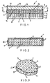
- An ultrasound detector comprising a layer of piezoelectric material (8) having first and second major surfaces (10, 16), and an array of electrodes (2) adjacent and facing one of the major surfaces (10), the electrodes (2) being electrically coupled to the material (8) by an ohmic or capacitive coupling (12).
- A detector as claimed in claim 1, characterised in that the electrodes (2) are embedded in an electrically insulating matrix (4).
- A detector as claimed in claim 1 or 2, characterised in that the film of piezoelectric material (8) is substantially planar.
- A detector as claimed in claim 1, 2 or 3, characterised in that the electrodes (2) are bonded to the piezoelectric material (8) by a non-conductive adhesive (12).
- A detector as claimed in any one of claims 1 to 4, characterised in that the piezoelectric material (8) is flexible.
- A detector as claimed in any one of claim 1 to 5, characterised in that the electrodes (2) are separated from each other by an electrical ground (26).
- A detector as claimed in any one of claims 1 to 6, characterised in that the electrodes (2) are of conductive polymer material.
- A method of measuring an ultrasound field, the method comprising providing a detector as defined in claim 1 and reading and analysing electronically signals produced in the electrodes (2) when the detector (1) is exposed to the ultrasound field.
Applications Claiming Priority (3)
| Application Number | Priority Date | Filing Date | Title |
|---|---|---|---|
| GB9502999 | 1995-02-16 | ||
| GBGB9502999.7A GB9502999D0 (en) | 1995-02-16 | 1995-02-16 | Ultrasound detector |
| PCT/GB1996/000368 WO1996025244A1 (en) | 1995-02-16 | 1996-02-16 | Electrical coupling for piezoelectric ultrasound detector |
Publications (2)
| Publication Number | Publication Date |
|---|---|
| EP0809542A1 EP0809542A1 (en) | 1997-12-03 |
| EP0809542B1 true EP0809542B1 (en) | 1999-12-22 |
Family
ID=10769679
Family Applications (1)
| Application Number | Title | Priority Date | Filing Date |
|---|---|---|---|
| EP96903100A Expired - Lifetime EP0809542B1 (en) | 1995-02-16 | 1996-02-16 | Electrical coupling for piezoelectric ultrasound detector |
Country Status (8)
| Country | Link |
|---|---|
| US (1) | US6094988A (en) |
| EP (1) | EP0809542B1 (en) |
| AT (1) | ATE187904T1 (en) |
| AU (1) | AU720051B2 (en) |
| DE (1) | DE69605770T2 (en) |
| GB (2) | GB9502999D0 (en) |
| NO (1) | NO973773L (en) |
| WO (1) | WO1996025244A1 (en) |
Families Citing this family (28)
| Publication number | Priority date | Publication date | Assignee | Title |
|---|---|---|---|---|
| US6012779A (en) | 1997-02-04 | 2000-01-11 | Lunar Corporation | Thin film acoustic array |
| JP2000114918A (en) * | 1998-10-05 | 2000-04-21 | Mitsubishi Electric Corp | Surface acoustic wave device and its manufacture |
| US6980017B1 (en) * | 1999-03-10 | 2005-12-27 | Micron Technology, Inc. | Test interconnect for bumped semiconductor components and method of fabrication |
| US6360611B1 (en) * | 2000-04-21 | 2002-03-26 | Kohji Toda | Device for ultrasound radiation into a material |
| EP2430998A3 (en) * | 2000-07-13 | 2014-01-22 | ReCor Medical, Inc. | Ultrasonic emitter configured to receive a liquid |
| US6635054B2 (en) * | 2000-07-13 | 2003-10-21 | Transurgical, Inc. | Thermal treatment methods and apparatus with focused energy application |
| US6763722B2 (en) * | 2001-07-13 | 2004-07-20 | Transurgical, Inc. | Ultrasonic transducers |
| US6707236B2 (en) * | 2002-01-29 | 2004-03-16 | Sri International | Non-contact electroactive polymer electrodes |
| US20040082859A1 (en) | 2002-07-01 | 2004-04-29 | Alan Schaer | Method and apparatus employing ultrasound energy to treat body sphincters |
| JP4104445B2 (en) * | 2002-12-12 | 2008-06-18 | 株式会社イデアルスター | Linear device |
| WO2004073505A2 (en) | 2003-02-20 | 2004-09-02 | Prorhythm, Inc. | Cardiac ablation devices |
| US20050075571A1 (en) * | 2003-09-18 | 2005-04-07 | Siemens Medical Solutions Usa, Inc. | Sound absorption backings for ultrasound transducers |
| GB0526381D0 (en) * | 2005-12-23 | 2006-02-08 | Rue De Int Ltd | Transducer |
| WO2007136566A2 (en) | 2006-05-19 | 2007-11-29 | Prorhythm, Inc. | Ablation device with optimized input power profile and method of using the same |
| US8139827B2 (en) * | 2006-05-25 | 2012-03-20 | Ultra-Scan Corporation | Biometrical object reader having an ultrasonic wave manipulation device |
| US20080228074A1 (en) * | 2007-03-12 | 2008-09-18 | Ketterling Jeffrey A | System and method for measuring acoustic pressure at multiple locations simultaneously |
| EP2174360A4 (en) | 2007-06-29 | 2013-12-11 | Artificial Muscle Inc | Electroactive polymer transducers for sensory feedback applications |
| EP2376011B1 (en) | 2009-01-09 | 2019-07-03 | ReCor Medical, Inc. | Apparatus for treatment of mitral valve insufficiency |
| EP2239793A1 (en) | 2009-04-11 | 2010-10-13 | Bayer MaterialScience AG | Electrically switchable polymer film structure and use thereof |
| EP2283935A1 (en) * | 2009-08-13 | 2011-02-16 | Fraunhofer-Gesellschaft zur Förderung der angewandten Forschung e.V. | Ultrasound converter system and method for its operation |
| SG193003A1 (en) | 2011-03-01 | 2013-10-30 | Bayer Ip Gmbh | Automated manufacturing processes for producing deformable polymer devices and films |
| WO2012129357A2 (en) | 2011-03-22 | 2012-09-27 | Bayer Materialscience Ag | Electroactive polymer actuator lenticular system |
| EP2828901B1 (en) | 2012-03-21 | 2017-01-04 | Parker Hannifin Corporation | Roll-to-roll manufacturing processes for producing self-healing electroactive polymer devices |
| KR20150031285A (en) | 2012-06-18 | 2015-03-23 | 바이엘 인텔렉쳐 프로퍼티 게엠베하 | Stretch frame for stretching process |
| US9590193B2 (en) | 2012-10-24 | 2017-03-07 | Parker-Hannifin Corporation | Polymer diode |
| DE102013201928A1 (en) | 2013-02-06 | 2014-08-07 | Richard Wolf Gmbh | Electroacoustic transducer for producing acoustic waves e.g. shock waves in medical field, has piezoelectric elements whose one side is provided with electrode which is electrical insulated in relation to piezoelectric elements |
| GB2555835B (en) * | 2016-11-11 | 2018-11-28 | Novosound Ltd | Ultrasound transducer |
| EP3817075B1 (en) * | 2019-10-29 | 2022-08-10 | Continental Automotive Technologies GmbH | Piezoceramic ultrasonic transducer |
Family Cites Families (9)
| Publication number | Priority date | Publication date | Assignee | Title |
|---|---|---|---|---|
| US4950936A (en) | 1981-03-09 | 1990-08-21 | The United States Of America As Represented By The Secretary Of The Navy | Piezoelectric sandwich polymer transducer |
| JPS5943356A (en) * | 1982-09-06 | 1984-03-10 | Kureha Chem Ind Co Ltd | Ultrasonic probe |
| US4805157A (en) | 1983-12-02 | 1989-02-14 | Raytheon Company | Multi-layered polymer hydrophone array |
| US4555953A (en) * | 1984-04-16 | 1985-12-03 | Paolo Dario | Composite, multifunctional tactile sensor |
| DE3568093D1 (en) * | 1984-05-30 | 1989-03-09 | Siemens Ag | Hydrophone |
| US4914565A (en) * | 1987-05-22 | 1990-04-03 | Siemens Aktiengesellschaft | Piezo-electric transducer having electrodes that adhere well both to ceramic as well as to plastics |
| JPH01170300A (en) * | 1987-12-25 | 1989-07-05 | Taiyo Yuden Co Ltd | Piezoelectric element plate |
| GB8928533D0 (en) * | 1989-12-18 | 1990-02-21 | Lesny Jan | Ultrasonic instrument |
| US5230921A (en) * | 1992-08-04 | 1993-07-27 | Blacktoe Medical, Inc. | Flexible piezo-electric membrane |
-
1995
- 1995-02-16 GB GBGB9502999.7A patent/GB9502999D0/en active Pending
-
1996
- 1996-02-16 AU AU47251/96A patent/AU720051B2/en not_active Ceased
- 1996-02-16 AT AT96903100T patent/ATE187904T1/en not_active IP Right Cessation
- 1996-02-16 WO PCT/GB1996/000368 patent/WO1996025244A1/en active IP Right Grant
- 1996-02-16 GB GB9717274A patent/GB2314205A/en not_active Withdrawn
- 1996-02-16 EP EP96903100A patent/EP0809542B1/en not_active Expired - Lifetime
- 1996-02-16 DE DE69605770T patent/DE69605770T2/en not_active Expired - Fee Related
- 1996-02-16 US US08/875,982 patent/US6094988A/en not_active Expired - Fee Related
-
1997
- 1997-08-15 NO NO973773A patent/NO973773L/en not_active Application Discontinuation
Also Published As
| Publication number | Publication date |
|---|---|
| GB9502999D0 (en) | 1995-04-05 |
| DE69605770T2 (en) | 2000-07-20 |
| WO1996025244A1 (en) | 1996-08-22 |
| NO973773L (en) | 1997-10-15 |
| NO973773D0 (en) | 1997-08-15 |
| EP0809542A1 (en) | 1997-12-03 |
| GB9717274D0 (en) | 1997-10-22 |
| ATE187904T1 (en) | 2000-01-15 |
| DE69605770D1 (en) | 2000-01-27 |
| AU720051B2 (en) | 2000-05-25 |
| GB2314205A (en) | 1997-12-17 |
| AU4725196A (en) | 1996-09-04 |
| US6094988A (en) | 2000-08-01 |
Similar Documents
| Publication | Publication Date | Title |
|---|---|---|
| EP0809542B1 (en) | Electrical coupling for piezoelectric ultrasound detector | |
| US6936008B2 (en) | Ultrasound system with cableless coupling assembly | |
| US6308389B1 (en) | Ultrasonic transducer and manufacturing method therefor | |
| US20090069689A1 (en) | Ultrasonic probe and ultrasonic imaging apparatus | |
| US20020073781A1 (en) | Ultrasonic probe, method of manufacturing the same and ultrasonic diagnosis apparatus | |
| KR100947404B1 (en) | Electrical connection system for ultrasonic receiver array | |
| US11806752B2 (en) | Ultrasound transducer and method for wafer level front face attachment | |
| US20130134834A1 (en) | Backing member, ultrasonic probe, and ultrasonic image display apparatus | |
| EP2014236A1 (en) | Ultrasonic probe | |
| WO1993007728A1 (en) | Ultrasonic wave probe | |
| GB2432671A (en) | Ultrasonic transducer with transmitter layer and receiver layer each having elongated electrodes | |
| KR101435011B1 (en) | Ultrasound Probe and Manufacturing Method thereof | |
| JP2004363746A (en) | Ultrasonic probe and its manufacturing method | |
| EP0637470A2 (en) | Backing layer for acoustic transducer array | |
| US5657295A (en) | Ultrasonic transducer with adjustable elevational aperture and methods for using same | |
| JPH0965489A (en) | Ultrasonic probe | |
| JPH05123317A (en) | Two-dimensional array ultrasonic probe | |
| JP3325368B2 (en) | Ultrasonic probe and manufacturing method thereof | |
| JP2000214144A (en) | Two-dimensional array ultrasonic probe | |
| JP7066092B1 (en) | How to produce sensor devices and sensor devices | |
| JPH04203994A (en) | Ultrasonic probe | |
| JPS59137039A (en) | Ultrasonic probe | |
| KR20220115445A (en) | Ultrasound prove | |
| Ketterling et al. | Linear hydrophone arrays for measurement of shock wave lithotripter acoustic fields | |
| KR20180068586A (en) | Probe for ultrasonic diagnostic apparatus |
Legal Events
| Date | Code | Title | Description |
|---|---|---|---|
| PUAI | Public reference made under article 153(3) epc to a published international application that has entered the european phase |
Free format text: ORIGINAL CODE: 0009012 |
|
| 17P | Request for examination filed |
Effective date: 19970903 |
|
| AK | Designated contracting states |
Kind code of ref document: A1 Designated state(s): AT BE CH DE DK ES FR GB IE IT LI NL SE |
|
| 17Q | First examination report despatched |
Effective date: 19971222 |
|
| GRAG | Despatch of communication of intention to grant |
Free format text: ORIGINAL CODE: EPIDOS AGRA |
|
| GRAG | Despatch of communication of intention to grant |
Free format text: ORIGINAL CODE: EPIDOS AGRA |
|
| GRAH | Despatch of communication of intention to grant a patent |
Free format text: ORIGINAL CODE: EPIDOS IGRA |
|
| TPAD | Observations filed by third parties |
Free format text: ORIGINAL CODE: EPIDOS TIPA |
|
| GRAH | Despatch of communication of intention to grant a patent |
Free format text: ORIGINAL CODE: EPIDOS IGRA |
|
| GRAA | (expected) grant |
Free format text: ORIGINAL CODE: 0009210 |
|
| AK | Designated contracting states |
Kind code of ref document: B1 Designated state(s): AT BE CH DE DK ES FR GB IE IT LI NL SE |
|
| PG25 | Lapsed in a contracting state [announced via postgrant information from national office to epo] |
Ref country code: SE Free format text: THE PATENT HAS BEEN ANNULLED BY A DECISION OF A NATIONAL AUTHORITY Effective date: 19991222 Ref country code: NL Free format text: LAPSE BECAUSE OF FAILURE TO SUBMIT A TRANSLATION OF THE DESCRIPTION OR TO PAY THE FEE WITHIN THE PRESCRIBED TIME-LIMIT Effective date: 19991222 Ref country code: LI Free format text: LAPSE BECAUSE OF FAILURE TO SUBMIT A TRANSLATION OF THE DESCRIPTION OR TO PAY THE FEE WITHIN THE PRESCRIBED TIME-LIMIT Effective date: 19991222 Ref country code: IT Free format text: LAPSE BECAUSE OF FAILURE TO SUBMIT A TRANSLATION OF THE DESCRIPTION OR TO PAY THE FEE WITHIN THE PRE;WARNING: LAPSES OF ITALIAN PATENTS WITH EFFECTIVE DATE BEFORE 2007 MAY HAVE OCCURRED AT ANY TIME BEFORE 2007. THE CORRECT EFFECTIVE DATE MAY BE DIFFERENT FROM THE ONE RECORDED.SCRIBED TIME-LIMIT Effective date: 19991222 Ref country code: ES Free format text: THE PATENT HAS BEEN ANNULLED BY A DECISION OF A NATIONAL AUTHORITY Effective date: 19991222 Ref country code: CH Free format text: LAPSE BECAUSE OF FAILURE TO SUBMIT A TRANSLATION OF THE DESCRIPTION OR TO PAY THE FEE WITHIN THE PRESCRIBED TIME-LIMIT Effective date: 19991222 Ref country code: BE Free format text: LAPSE BECAUSE OF FAILURE TO SUBMIT A TRANSLATION OF THE DESCRIPTION OR TO PAY THE FEE WITHIN THE PRESCRIBED TIME-LIMIT Effective date: 19991222 Ref country code: AT Free format text: LAPSE BECAUSE OF FAILURE TO SUBMIT A TRANSLATION OF THE DESCRIPTION OR TO PAY THE FEE WITHIN THE PRESCRIBED TIME-LIMIT Effective date: 19991222 |
|
| REF | Corresponds to: |
Ref document number: 187904 Country of ref document: AT Date of ref document: 20000115 Kind code of ref document: T |
|
| REG | Reference to a national code |
Ref country code: CH Ref legal event code: EP |
|
| REF | Corresponds to: |
Ref document number: 69605770 Country of ref document: DE Date of ref document: 20000127 |
|
| PG25 | Lapsed in a contracting state [announced via postgrant information from national office to epo] |
Ref country code: IE Free format text: LAPSE BECAUSE OF NON-PAYMENT OF DUE FEES Effective date: 20000216 |
|
| REG | Reference to a national code |
Ref country code: IE Ref legal event code: FG4D |
|
| PG25 | Lapsed in a contracting state [announced via postgrant information from national office to epo] |
Ref country code: DK Free format text: LAPSE BECAUSE OF FAILURE TO SUBMIT A TRANSLATION OF THE DESCRIPTION OR TO PAY THE FEE WITHIN THE PRESCRIBED TIME-LIMIT Effective date: 20000322 |
|
| ET | Fr: translation filed | ||
| NLV1 | Nl: lapsed or annulled due to failure to fulfill the requirements of art. 29p and 29m of the patents act | ||
| REG | Reference to a national code |
Ref country code: CH Ref legal event code: PL |
|
| PLBE | No opposition filed within time limit |
Free format text: ORIGINAL CODE: 0009261 |
|
| STAA | Information on the status of an ep patent application or granted ep patent |
Free format text: STATUS: NO OPPOSITION FILED WITHIN TIME LIMIT |
|
| 26N | No opposition filed | ||
| REG | Reference to a national code |
Ref country code: IE Ref legal event code: MM4A |
|
| REG | Reference to a national code |
Ref country code: GB Ref legal event code: IF02 |
|
| PGFP | Annual fee paid to national office [announced via postgrant information from national office to epo] |
Ref country code: FR Payment date: 20030210 Year of fee payment: 8 |
|
| PGFP | Annual fee paid to national office [announced via postgrant information from national office to epo] |
Ref country code: DE Payment date: 20030227 Year of fee payment: 8 |
|
| PG25 | Lapsed in a contracting state [announced via postgrant information from national office to epo] |
Ref country code: DE Free format text: LAPSE BECAUSE OF NON-PAYMENT OF DUE FEES Effective date: 20040901 |
|
| PG25 | Lapsed in a contracting state [announced via postgrant information from national office to epo] |
Ref country code: FR Free format text: LAPSE BECAUSE OF NON-PAYMENT OF DUE FEES Effective date: 20041029 |
|
| REG | Reference to a national code |
Ref country code: FR Ref legal event code: ST |
|
| PGFP | Annual fee paid to national office [announced via postgrant information from national office to epo] |
Ref country code: GB Payment date: 20100202 Year of fee payment: 15 |
|
| GBPC | Gb: european patent ceased through non-payment of renewal fee |
Effective date: 20110216 |
|
| PG25 | Lapsed in a contracting state [announced via postgrant information from national office to epo] |
Ref country code: GB Free format text: LAPSE BECAUSE OF NON-PAYMENT OF DUE FEES Effective date: 20110216 |