EP0813198A2 - Recording and reproduction apparatus and method, and disk - Google Patents
Recording and reproduction apparatus and method, and disk Download PDFInfo
- Publication number
- EP0813198A2 EP0813198A2 EP97109583A EP97109583A EP0813198A2 EP 0813198 A2 EP0813198 A2 EP 0813198A2 EP 97109583 A EP97109583 A EP 97109583A EP 97109583 A EP97109583 A EP 97109583A EP 0813198 A2 EP0813198 A2 EP 0813198A2
- Authority
- EP
- European Patent Office
- Prior art keywords
- recording
- data
- disk
- link area
- reproduction unit
- Prior art date
- Legal status (The legal status is an assumption and is not a legal conclusion. Google has not performed a legal analysis and makes no representation as to the accuracy of the status listed.)
- Granted
Links
Images


Classifications
-
- G—PHYSICS
- G11—INFORMATION STORAGE
- G11B—INFORMATION STORAGE BASED ON RELATIVE MOVEMENT BETWEEN RECORD CARRIER AND TRANSDUCER
- G11B20/00—Signal processing not specific to the method of recording or reproducing; Circuits therefor
- G11B20/10—Digital recording or reproducing
- G11B20/12—Formatting, e.g. arrangement of data block or words on the record carriers
- G11B20/1217—Formatting, e.g. arrangement of data block or words on the record carriers on discs
-
- G—PHYSICS
- G11—INFORMATION STORAGE
- G11B—INFORMATION STORAGE BASED ON RELATIVE MOVEMENT BETWEEN RECORD CARRIER AND TRANSDUCER
- G11B20/00—Signal processing not specific to the method of recording or reproducing; Circuits therefor
- G11B20/10—Digital recording or reproducing
- G11B20/10009—Improvement or modification of read or write signals
- G11B20/10222—Improvement or modification of read or write signals clock-related aspects, e.g. phase or frequency adjustment or bit synchronisation
- G11B20/1024—Improvement or modification of read or write signals clock-related aspects, e.g. phase or frequency adjustment or bit synchronisation wherein a phase-locked loop [PLL] is used
-
- G—PHYSICS
- G11—INFORMATION STORAGE
- G11B—INFORMATION STORAGE BASED ON RELATIVE MOVEMENT BETWEEN RECORD CARRIER AND TRANSDUCER
- G11B27/00—Editing; Indexing; Addressing; Timing or synchronising; Monitoring; Measuring tape travel
- G11B27/10—Indexing; Addressing; Timing or synchronising; Measuring tape travel
- G11B27/19—Indexing; Addressing; Timing or synchronising; Measuring tape travel by using information detectable on the record carrier
- G11B27/28—Indexing; Addressing; Timing or synchronising; Measuring tape travel by using information detectable on the record carrier by using information signals recorded by the same method as the main recording
- G11B27/30—Indexing; Addressing; Timing or synchronising; Measuring tape travel by using information detectable on the record carrier by using information signals recorded by the same method as the main recording on the same track as the main recording
- G11B27/3027—Indexing; Addressing; Timing or synchronising; Measuring tape travel by using information detectable on the record carrier by using information signals recorded by the same method as the main recording on the same track as the main recording used signal is digitally coded
-
- G—PHYSICS
- G11—INFORMATION STORAGE
- G11B—INFORMATION STORAGE BASED ON RELATIVE MOVEMENT BETWEEN RECORD CARRIER AND TRANSDUCER
- G11B7/00—Recording or reproducing by optical means, e.g. recording using a thermal beam of optical radiation by modifying optical properties or the physical structure, reproducing using an optical beam at lower power by sensing optical properties; Record carriers therefor
- G11B7/007—Arrangement of the information on the record carrier, e.g. form of tracks, actual track shape, e.g. wobbled, or cross-section, e.g. v-shaped; Sequential information structures, e.g. sectoring or header formats within a track
- G11B7/00745—Sectoring or header formats within a track
-
- G—PHYSICS
- G11—INFORMATION STORAGE
- G11B—INFORMATION STORAGE BASED ON RELATIVE MOVEMENT BETWEEN RECORD CARRIER AND TRANSDUCER
- G11B20/00—Signal processing not specific to the method of recording or reproducing; Circuits therefor
- G11B20/10—Digital recording or reproducing
- G11B20/12—Formatting, e.g. arrangement of data block or words on the record carriers
- G11B20/1217—Formatting, e.g. arrangement of data block or words on the record carriers on discs
- G11B20/1258—Formatting, e.g. arrangement of data block or words on the record carriers on discs where blocks are arranged within multiple radial zones, e.g. Zone Bit Recording or Constant Density Recording discs, MCAV discs, MCLV discs
-
- G—PHYSICS
- G11—INFORMATION STORAGE
- G11B—INFORMATION STORAGE BASED ON RELATIVE MOVEMENT BETWEEN RECORD CARRIER AND TRANSDUCER
- G11B20/00—Signal processing not specific to the method of recording or reproducing; Circuits therefor
- G11B20/10—Digital recording or reproducing
- G11B20/12—Formatting, e.g. arrangement of data block or words on the record carriers
- G11B2020/1264—Formatting, e.g. arrangement of data block or words on the record carriers wherein the formatting concerns a specific kind of data
- G11B2020/1265—Control data, system data or management information, i.e. data used to access or process user data
- G11B2020/1267—Address data
-
- G—PHYSICS
- G11—INFORMATION STORAGE
- G11B—INFORMATION STORAGE BASED ON RELATIVE MOVEMENT BETWEEN RECORD CARRIER AND TRANSDUCER
- G11B20/00—Signal processing not specific to the method of recording or reproducing; Circuits therefor
- G11B20/10—Digital recording or reproducing
- G11B20/12—Formatting, e.g. arrangement of data block or words on the record carriers
- G11B2020/1264—Formatting, e.g. arrangement of data block or words on the record carriers wherein the formatting concerns a specific kind of data
- G11B2020/1265—Control data, system data or management information, i.e. data used to access or process user data
- G11B2020/1277—Control data, system data or management information, i.e. data used to access or process user data for managing gaps between two recordings, e.g. control data in linking areas, run-in or run-out fields, guard or buffer zones
-
- G—PHYSICS
- G11—INFORMATION STORAGE
- G11B—INFORMATION STORAGE BASED ON RELATIVE MOVEMENT BETWEEN RECORD CARRIER AND TRANSDUCER
- G11B20/00—Signal processing not specific to the method of recording or reproducing; Circuits therefor
- G11B20/10—Digital recording or reproducing
- G11B20/12—Formatting, e.g. arrangement of data block or words on the record carriers
- G11B2020/1264—Formatting, e.g. arrangement of data block or words on the record carriers wherein the formatting concerns a specific kind of data
- G11B2020/1265—Control data, system data or management information, i.e. data used to access or process user data
- G11B2020/1287—Synchronisation pattern, e.g. VCO fields
-
- G—PHYSICS
- G11—INFORMATION STORAGE
- G11B—INFORMATION STORAGE BASED ON RELATIVE MOVEMENT BETWEEN RECORD CARRIER AND TRANSDUCER
- G11B2220/00—Record carriers by type
- G11B2220/20—Disc-shaped record carriers
- G11B2220/21—Disc-shaped record carriers characterised in that the disc is of read-only, rewritable, or recordable type
- G11B2220/215—Recordable discs
- G11B2220/216—Rewritable discs
-
- G—PHYSICS
- G11—INFORMATION STORAGE
- G11B—INFORMATION STORAGE BASED ON RELATIVE MOVEMENT BETWEEN RECORD CARRIER AND TRANSDUCER
- G11B2220/00—Record carriers by type
- G11B2220/20—Disc-shaped record carriers
- G11B2220/25—Disc-shaped record carriers characterised in that the disc is based on a specific recording technology
- G11B2220/2537—Optical discs
-
- G—PHYSICS
- G11—INFORMATION STORAGE
- G11B—INFORMATION STORAGE BASED ON RELATIVE MOVEMENT BETWEEN RECORD CARRIER AND TRANSDUCER
- G11B7/00—Recording or reproducing by optical means, e.g. recording using a thermal beam of optical radiation by modifying optical properties or the physical structure, reproducing using an optical beam at lower power by sensing optical properties; Record carriers therefor
- G11B7/004—Recording, reproducing or erasing methods; Read, write or erase circuits therefor
- G11B7/0045—Recording
Definitions
- the present invention relates to a recording and reproduction apparatus and method, and a disk. More particularly, the present invention relates to a recording and reproduction apparatus and method, and a disk, in which thermal stress is prevented from accumulating on a recording medium when data is repeatedly recorded on a disk.
- a conventional recording apparatus records data by modulating the intensity of a laser beam on the basis of data to be recorded and radiating it onto a disk, and causing a physical change in a recording medium.
- data is recorded on the basis of address information prerecorded on a disk. Therefore, when data is recorded with specific address information being specified, the area where the data is recorded is predetermined on the disk.
- a signal for synchronization (hereinafter abbreviated as a synchronization signal) together with the data to be recorded in order to synchronize signals during reproduction. Since information (content) in such a synchronization signal is often determined according to the position (address) on the disk, a specific synchronization signal is provided for a predetermined address.
- the present invention has been achieved in view of such circumstances.
- the present invention makes it possible to prevent thermal stress from accumulating on a recording medium even when overwriting is performed on a rewritable-type disk and to record data continuously.
- the recording and reproduction apparatus of claim 1 comprises: division means for dividing data into blocks of a predetermined length; recording and reproduction unit formation means for forming a recording and reproduction unit by adding a front link area and a back link area of a predetermined length before and after the block, respectively; address detection means for detecting an address prerecorded on the rewritable-type disk; and recording means for recording the recording and reproduction unit on a predetermined area of the rewritable-type disk on the basis of an output from the address detection means.
- the recording and reproduction method of claim 10 comprises: a dividing step for dividing data into blocks of a predetermined length; a recording and reproduction unit formation step for forming a recording and reproduction unit by adding a front link area of a predetermined length and a back link area of a predetermined length before and after the block, respectively; an address detection step for detecting an address prerecorded on the rewritable-type disk; and a recording step for recording the recording and reproduction unit on a predetermined area of the rewritable-type disk on the basis of the address detected in the address detection step.
- a recording and reproduction unit formed in such a way that a front link area and a back link area are respectively added before and after data divided into a predetermined length is recorded thereon.
- the lengths of the front link area and the back link area are randomly changed so that the recording and reproduction unit has a fixed length.
- the division means divides data into blocks of a predetermined length
- the recording and reproduction unit formation means forms a recording and reproduction unit by respectively adding a front link area and a back link area of a predetermined length before and after the block
- the address detection means detects an address prerecorded on a rewritable-type disk
- the recording means records the recording and reproduction unit on a predetermined area of the rewritable-type disk on the basis of an output from the address detection means.
- data to be recorded is divided into blocks of a predetermined length by the division means, a front link area and a back link area are respectively added before and after the block, and a recording and reproduction unit to which the front and back link areas are added is recorded on a disk on the basis of the address detected by the address detection means.
- data is divided into blocks of a predetermined length in the division step, a recording and reproduction unit is formed by adding a front link area and a back link area of a predetermined length before and after the block, respectively, in the recording and reproduction unit formation step, the address prerecorded on a rewritable-type disk is detected in an address detection step, and the recording and reproduction unit is recorded on a predetermined area of the rewritable-type disk on the basis of an output from the address detection step in the recording step.
- data to be recorded is divided into blocks of a predetermined length in the division step, a front link area and a back link area are added respectively before and after the block, and a recording and reproduction unit to which the front link area and the back link area are added is recorded on a disk on the basis of the address detected in the address detection step.
- a recording and reproduction unit formed in such a way that a front link area and a back link area are respectively added before and after data divided into a predetermined length is recorded thereon, and the recording and reproduction unit is recorded with the lengths of the front link area and the back link area randomly changed so that the recording and reproduction unit has a fixed length.
- a recording and reproduction unit is formed in such a way that a front link area and a back link area whose lengths are randomly changed are respectively added before and after the data divided into a predetermined length, and the recording and reproduction unit is recorded.
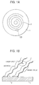
- Figs. 1A and 1B show an example of the construction of an optical disk in which a disk of the present invention is applied.
- a pre-groove 2 is formed beforehand in a spiral shape from the inner region toward the outer region in a disk (optical disk) 1.
- this pre-groove 2 may be formed in a concentric shape.
- the left and right side walls of the pre-groove 2 are wobbled on the basis of address information and are snaked in accordance with a frequency-modulated wave.
- One track has a plurality of wobbling address frames.
- Fig. 2 shows the structure (format) of a wobbling address frame.
- the wobbling address frame is formed of 48 bits, with the beginning 4 bits being a synchronization signal (Sync) indicating the start of a rewritable-type disk.
- the next 4 bits are made into a layer (Layer) indicating which layer from among a plurality of recording layers.
- the next 20 bits are made a track address (track number). Further, the next 4 bits indicate the frame number of the address frame.
- the subsequent 14 bits are made an error detection code (CRC), and an error detection code for data such that a synchronization signal (Sync) is excluded is recorded.
- the last 2 bits (Reserved) are kept in reserve for future use.
- the wobbling address frame is recorded in a CAV disk shape whose rotational angular velocity is fixed, for example, for an amount of 8 address frames per one track (one rotation). Therefore, as frame numbers in Fig. 2, for example, values from 0 to 7 are recorded.
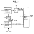
- Fig. 3 shows an example of the construction of a wobbling signal generation circuit which generates a wobbling signal for wobbling the pre-groove 2 on the basis of the address frame of the format shown in Fig. 2.
- a generation circuit 11 generates a signal having a frequency of 115.2 kHz.
- the signal generated from the generation circuit 11 is supplied to a division circuit 12 whereby the signal is divided by a value 7.5, and is supplied as a biphase clock signal having a frequency of 15.36 kHz to a biphase modulation circuit 13.
- ADIP Address In Pre-groove
- the biphase modulation circuit 13 biphase-modulates a biphase clock supplied from the division circuit 12 by ADIP data (address data) supplied from a circuit (not shown) and outputs a biphase signal to an FM modulation circuit 15.
- a carrier having a frequency of 57.6 kHz obtained by dividing a signal of 115.2 kHz generated by the generation circuit 11 with a value 2 by means of a divider 14 is further input to the FM modulation circuit 15.
- the FM modulation circuit 15 frequency-modulates the carrier input from the divider 14 by a biphase signal input from the biphase modulation circuit 13 and outputs a frequency-modulated signal obtained thereby.
- the left and right side walls of the pre-groove 2 of the disk 1 are formed (wobbled) in accordance with this frequency-modulated signal.
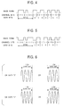
- Figs. 4 and 5 show examples of a biphase signal output from the biphase modulation circuit 13.
- SYNC synchronization pattern
- Fig. 5 shows the leading bit is 1, as shown in Fig. 5, "00010111” in a phase opposite to the case shown in Fig. 4 is used.
- SYNC is made a unique pattern as an exception to the rule which does not appear in the modulation.
- the FM modulation circuit 15 frequency-modulates a carrier supplied from the divider 14 as shown in Fig. 6 in accordance with the biphase signal shown in Fig. 4 or 5.
- the FM modulation circuit 15 when the channel bit data (biphase signal) is 0, the FM modulation circuit 15 outputs a carrier of 3.5 waves in a period corresponding to the length of half of one data bit.
- This carrier of 3.5 waves is a carrier which begins from a positive half wave or a negative half wave.
- a carrier of 4 waves is output in a period corresponding to the length of half of one data bit.
- This carrier of 4 waves also is a carrier which begins from a positive half wave or a negative half wave.
- the carrier of 57.6 kHz input to the FM modulation circuit 15 corresponds to a 7.5 wave.
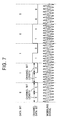
- Fig. 7 shows an example of a frequency-modulated wave output in this way from the FM modulation circuit 15.
- the first data bit is made 0, and its channel data bits are made 00.
- a carrier of 3.5 waves which begins from a positive half wave from the starting point is selected.
- the termination point of the carrier terminates at a positive half wave. Therefore, with respect to the next channel data bit 0, a 3.5 wave which begins from a negative half wave is selected, and thus a frequency-modulated wave of a total of 7 waves is formed with respect to data bit 0.
- This data bit 0 is followed by data bit 1 (channel bit 10). Since the 3.5 waves of the channel data bit corresponding to the previous data bit 0 terminate at a negative half wave, a carrier of 4 waves of the beginning channel data bit 1 corresponding to data bit 1, which begins from a positive half wave, is selected. Since the 4 waves of the channel data bit 1 terminate at a negative half wave, the 4 waves of the next channel data bit 0, which begin from a positive half wave, are selected.
- carriers of 7.5 waves, 8 waves and 7 waves in correspondence with data bit 1 (channel data bit 10), data bit 0 (channel data bit 11), and data bit 0 (channel data bit 00), are formed in such a manner as to be continuous at the boundary portions (the beginning point and the termination point) of the data bits and are output.
- the length of the channel bits is made an integral multiple of 1/2 of the wavelength of the carrier in the case of 7, 7.5 or 8 waves. That is, the length of the channel bits is made 7 times 1/2 of the wavelength of the carrier (frequency-modulated wave) of 7 waves, and is made 8 times 1/2 of the wavelength of the carrier (frequency-modulated wave) of 8 waves. Further, the length of the channel bits is made 7 times 1/2 of 7.5 waves (when the channel bit is 0), and is made 8 times thereof (when the channel bit is 1).
- the boundary portion (the beginning point or the termination point) of the channel bits which are biphase-modulated is made a zero-cross point of the frequency-modulated wave.
- the boundary portions (the beginning point and the termination point) of the data bits are made to correspond to the edges (the zero-cross points) of the frequency-modulated wave.
- a clock is generated with a clock synchronization mark as a reference.
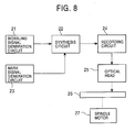
- Fig. 8 shows an example of the construction of a recording apparatus (disk formation apparatus) for manufacturing a disk 1 having a pre-groove.
- a wobbling signal generation circuit 21 has the construction shown in Fig. 3 and supplies a frequency-modulated signal output from the FM modulation circuit 15 to a synthesis circuit 22.
- a mark signal generation circuit 23 generates a clock synchronization mark signal at a predetermined timing and outputs it to the synthesis circuit 22.
- the synthesis circuit 22 synthesizes a frequency-modulated signal output from the wobbling signal generation circuit 21 and a clock synchronization mark signal output from the mark signal generation circuit 23 and outputs the result to a recording circuit 24.
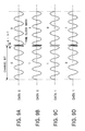
- the synthesis circuit 22 synthesizes the clock synchronization mark (Fine Clock Mark) onto a carrier supplied from the wobbling signal generation circuit 21, as shown in Figs. 9A to 9D.
- the clock synchronization mark is made a length from 6 to 14T (T is the length of a bit cell).
- a clock synchronization mark of a frequency higher than the modulation frequency (57.6 kHz) of the address information is synthesized at the zero-cross point of the carrier of the respective data center (the switching point of the channel bits). This clock synchronization mark is recorded on every data bit or every predetermined number of data bits.
- Insertion of a clock synchronization mark at the zero-cross point of the wobbling frequency-modulated wave corresponding to the center (switching point of the channel data bits) of the address data bits as described above reduces amplitude variations of the clock synchronization mark, making it easy to detect the clock synchronization mark.
- the FM modulation circuit 15 when the channel data bit is 0, frequency modulation is performed so as to shift the frequency, for example, by -5% from the center frequency, and when the channel data bit is 1, frequency modulation is performed so as to shift the frequency, for example, by +5% from the center frequency, the data bits or the boundary portion of the channel data bits and the zero-cross point of the frequency-modulated wave do not coincide with each other, and thus it is likely to erroneously detect the channel data bits (or the data bits). Further, the insertion position of the clock synchronization mark is not necessarily a zero-cross point and is superimposed onto a point of the frequency-modulated wave having a predetermined amplitude value.
- the level of the clock synchronization mark is increased or decreased by an amount corresponding to the amplitude value, and detection of the clock synchronization mark becomes difficult.
- the clock synchronization mark is always placed at the zero-cross point of the frequency-modulated wave, the detection (identification from the frequency-modulated wave) of the clock synchronization mark is made easy.
- the recording circuit 24 controls an optical head 25 in accordance with a signal supplied from the synthesis circuit 22 in order to generate laser light for forming a pre-groove (including a clock synchronization mark) on an original disk 26.
- a spindle motor 27 causes the original disk 26 to rotate at a fixed angular velocity (CAV).
- the frequency-modulated wave generated by the wobbling signal generation circuit 21 is synthesized, in the synthesis circuit 22, onto the clock synchronization mark signal output from the mark signal generation circuit 23, and is input to the recording circuit 24.
- the recording circuit 24 controls the optical head 25 in accordance with the signal input from the synthesis circuit 22 in order to generate laser light.
- the laser light generated from the optical head 25 is radiated onto the original disk 26 rotated at a fixed angular velocity by the spindle motor 27.
- the original disk 26 is developed, a stamper is made from this original disk 26, and disks 1 are formed as a number of replicas from the stamper. This makes it possible to obtain a disk 1 on which a pre-groove 2 having the above-described clock synchronization mark is formed.
- Fig. 10 shows an example of the construction of an optical disk recording and reproduction apparatus for recording data to or reproducing data from the disk 1 obtained in this way.
- a spindle motor 31 causes the disk 1 to rotate at a predetermined angular velocity.
- An optical head 32 (recording means, recording step) radiates laser light onto the disk 1 in order to record data onto the disk 1 and reproduce data from the light reflected therefrom.
- a recording and reproducing circuit 33 (recording and reproduction unit formation means, recording and reproduction unit formation step, addition means, addition step, second addition means) temporarily stores recording data input from an apparatus (not shown) in a memory 34 (division means, division step), reads one cluster of data when this one cluster of data (or may also be one sector of data), which is a recording unit, is stored in the memory 34, and, for example, modulates the data by a predetermined method and then outputs the modulated data to the optical head 32. Further, the recording and reproducing circuit 33 appropriately demodulates the data input from the optical head 32 and outputs the demodulated data to an apparatus (not shown).
- the recording and reproducing circuit 33 adds a front link area and a back link area to the recording data and adds a synchronization signal to these link areas, and then outputs the result.
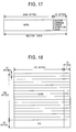
- An address generation and reading circuit 35 (address detection means, address detection step) generates a data address (sector address) (will be described later with reference to Fig. 17) to be recorded within the track (pre-groove 2) under control from a control circuit 38 and outputs the data address to the recording and reproducing circuit 33.
- the recording and reproducing circuit 33 adds this address to the recording data supplied from the apparatus (not shown) and outputs the data to the optical head 32. Further, when address data is contained within the reproduction data which is reproduced from the tracks of the disk 1 by the optical head 32, the recording and reproducing circuit 33 separates this address data and outputs it to the address generation and reading circuit 35.
- the address generation and reading circuit 35 outputs the read address to the control circuit 38.
- a mark detection circuit 36 detects components corresponding to the clock synchronization mark from an RF signal reproduced and output by the optical head 32.
- a frame address detection circuit 37 reads address information (the track number and the frame number in Fig. 2) contained in the wobbling signal from the RF signal output from the optical head 32 and supplies the address information to a cluster counter 46 and the control circuit 38.
- a mark cycle detection circuit 40 determines the periodicity of detected pulses which are output when the mark detection circuit 36 detects a clock synchronization mark. That is, since the clock synchronization mark is generated at a fixed cycle, a check is made to determine if the detected pulses input from the mark detection circuit 36 are detected pulses generated at this current fixed cycle. If the pulses are detected pulses generated at this fixed cycle, pulses which are synchronized with the detected pulses are generated, and output to a phase comparator 42 of a PLL circuit 41 of a latter stage. Further, in a case in which detected pulses are not input at a fixed cycle, the mark cycle detection circuit 40 generates a pseudo pulse at a predetermined timing so that the PLL circuit 41 of the latter stage does not lock to an incorrect phase.
- the PLL circuit 41 has, in addition to the phase comparator 42, a low-pass filter (LPF) 43, a voltage control oscillator (VCO) 44, and a frequency divider 45.
- the phase comparator 42 compares the phase of an input from the mark cycle detection circuit 40 with that of an input from the frequency divider 45 and outputs a difference between the phases.
- the low-pass filter 43 smooths the phase difference signal output from the phase comparator 42 and outputs the signal to the VCO 44.
- the VCO 44 generates a clock with a phase corresponding to the output from the low-pass filter 43 and outputs the clock to the frequency divider 45.
- the frequency divider 45 frequency-divides the clock input from the VCO 44 by a predetermined value (a value specified by the control circuit 38) and outputs the frequency-divided result to the phase comparator 42.
- the clock output from the VCO 44 is supplied to each circuit and also to the cluster counter 46.
- the cluster counter 46 counts the number of clocks output from the VCO 44 using the frame address supplied from the frame address detection circuit 37 as a reference, generates a cluster start pulse when the counted value reaches a predetermined value (a value corresponding to the length of one cluster) which is set previously, and outputs the value to the control circuit 38.
- a thread motor 39 which is controlled by the control circuit 38, transports the optical head 32 to a predetermined track position of the disk 1. Further, the control circuit 38 controls the spindle motor 31 so as to rotate the disk 1 at a predetermined angular velocity (CAV).
- CAV angular velocity
- a ROM 47 has stored therein, a table which defines the correspondence relationship between track numbers (Fig. 2) in the address frame and zones which separate the data recording areas of the disk 1, and, as required, a table which defines the relationship between zones and a band (the details of which will be described later) to which a zone corresponds.
- the control circuit 38 records or reproduces data to and from a plurality of divided zones (in this embodiment, m + 2 zones of the 0-th zone to the m + 1 zone).
- this data frame is a unit of blocks of data
- the number of data frames per one track is set to n + 8.
- the number of data frames increases by 8 than an adjacent zone of the inner region.
- the number of data frames reaches n + 8 ⁇ (m + 1) .
- the m-th zone is formed from the radius position at which a capacity of n + 8 ⁇ m frames can be obtained at the same linear density as the innermost-region linear density of the 0-th zone.
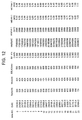
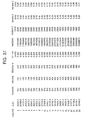
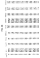
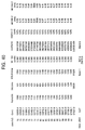
- the recording and reproducing area is divided into 92 zones, as shown in Figs. 12 to 15.
- the 0-th zone in which the disk radius is 24 mm, there are 520 frames per one track (one rotation). As the zone is incremented by 1, there is an increase of 8 frames per one track.
- zone CLD Constant Linear Density
- data of each column respectively indicate the zone number, the radius, the number of frames per one track, the number of tracks per one zone, the number (number of clusters) of recording and reproduction units (blocks) per one zone, the minimum linear density within the zone, the capacity of the zone, the rotational velocity of the zone, the minimum linear velocity of the zone, and the maximum linear velocity of the zone.
- the rotational velocity indicates the number of rotations per minute when the data transfer rate is set at 11.08 Mbps.
- the number of tracks in each zone is fixed to 424. This number of tracks is made the same value as the number (the number of frames of an ECC block) (will be described later with reference to Fig. 20) of frames in one recording and reproduction unit.
- the number of tracks in each zone is made one times the number of data frames (424 frames) which constitute the recording and reproduction unit, the number may be an integral multiple thereof. This prevents excess data frames from occurring, and an integral number of recording and reproduction units (blocks) are placed in each zone, making it possible to improve zoning efficiency. As a result, it is possible to obtain a capacity which is larger than zone CAV and close to zone CLV, though smaller than zone CLV.
- the optical head 32 radiates laser light onto the optical disk 1 and outputs an RF signal obtained from the light reflected therefrom.
- the frame address detection circuit 37 reads wobbling information (address information) from the RF signal, and outputs the read result to the control circuit 38 and also to the cluster counter 46. Further, this wobbling information is input to the mark detecting circuit 36 whereby a clock synchronization mark is detected and supplied to the mark cycle detection circuit 40.
- the mark cycle detection circuit 40 determines the periodicity of the clock synchronization mark, generates a predetermined pulse corresponding thereto, and outputs the pulse to the PLL circuit 41.
- the PLL circuit 41 generates a clock (recording clock) which is synchronized with this pulse and supplies the clock to the cluster counter 46.
- the control circuit 38 is capable of detecting the position of a reference clock synchronization mark in one track (one rotation) from the frame address (frame number) supplied from the frame address detection circuit 37. For example, with the clock synchronization mark detected at the beginning of a frame (address frame) of frame number 0 as a reference, it becomes possible to access any desired position (any desired position during one rotation) on the track on the basis of the count value of the recording clock.
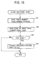
- control circuit 38 further performs a clock switching process such as that shown in the flowchart of Fig. 16.
- step S1 the control circuit 38 reads the track number from the frame address of the access point output from the frame address detection circuit 37. Then, in step S2, a zone corresponding to the track number read in step S1 is read from the table stored in the ROM 47. As described above, the table in the ROM 47 has prestored therein information on to which of the 0-th to 92-th zones the track of each number belongs.
- step S3 a check is made to determine if the track number just read indicates a new zone different from the zone which has been accessed up until then.
- the process proceeds to step S4 where the control circuit 38 controls the frequency divider 45 in order to set a frequency-dividing ratio corresponding to the new zone.
- a recording clock of a frequency different for each zone is output from the VCO 44.
- step S3 when it is determined in step S3 that the current zone is not a new zone, the process in step 4 is skipped. That is, the frequency-dividing ratio is kept as it is without being changed.
- data is recorded in units of one cluster (32 kilobytes), and this cluster is structured as described below.
- This overhead contains a sector address (address generated or read by the address generation and reading circuit 35 in Fig. 10) and an error detection code for error detection.
- PI 10-byte inner code
- PO 16-byte outer code
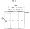
- data of 208 ⁇ 182 bytes shown in Fig. 19, as shown in Fig. 20, is divided into two parts in the vertical direction, one frame is formed into data of 91 bytes, and thus the data is formed into data of 208 ⁇ 2 frames.
- link data (data of the link area) of 4 ⁇ 2 frames is added (more precisely, as will be described later with reference to Fig. 23, a part of data for 8 frames is recorded onto the start of the cluster, and the remainder is recorded onto the end of the cluster) to the head of this data of 208 ⁇ 2 frames.
- a 2-byte frame synchronization signal (FS) is further added to the head of the 91-byte frame data.
- one cluster is formed of 16 sectors and one sector is formed of 26 frames.
- Fig. 21 shows each frame of a ROM disk (read-only disk) and a RAM disk (rewritable-type disk), and the structure of a frame synchronization signal.
- ROM disk read-only disk
- RAM disk rewritable-type disk
- frame synchronization signals SY0 to SY7 are added to the head of each frame.
- a link area of 8 frames is added followed by 13 rows of data, i.e., data of 26 frames, and then data of 26 frames is added.
- the structures of the frame synchronization signal of the data area of the RAM disk and the frame synchronization signal of the data area of the ROM disk are the same.
- the frame synchronization signal of the link area of the RAM disk is formed the same as the end portion of the frame synchronization signal of the data area. That is, SY1 to SY4 and SY7 of the link area are the same patterns as the 10-th to 13-th rows of the data area. With such a construction, it becomes possible to reproduce a RAM disk by a reproduction apparatus exclusively used for ROM disks.
- a reproduction apparatus exclusively used for ROM disks is formed in such a way that, when 8 frame synchronization signals SY1, SY7, SY2, SY7, SY3, SY7, SY4, and SY7 stored in the 10-th to 13-th rows of the data blocks are detected, the reproduction apparatus recognizes the next data to be the beginning portion of a data block. Therefore, by storing these 8 frame synchronization signals in the link area, it is possible to cause the reproduction apparatus to recognize the beginning portion of the data area which follows the link area.
- Fig. 22 shows an example of the frame synchronization signals SY0 to SY7 shown in Fig. 21.
- a frame synchronization signal is 2-byte data
- data after conversion is shown in the channel bit data; therefore, the data length of each frame synchronization signal is 32 bits (4 bytes).
- a link area is formed of 8 frames and is inserted between data blocks of 32 kilobytes.
- Each RW unit (recording and reproduction unit) is formed of: slice/PLL data which is a front link area of a 32-kilobyte data block or link data, such as frame synchronization signals SY1 to SY7; a 32-kilobyte data block; a postamble which is a back link area of the 32-kilobyte data block; and a postguard.
- a slice is data for setting the time constant for binarizing reproduction data
- a PLL is data for reproducing a clock.
- any of state 1 to state 4 is selected and added thereto, as described above with reference to Fig. 22.
- the postguard is an area for absorbing recording jitter which occurs in response to decentering of the disk, recording sensitivity of the disk and the like. Further, the postguard prevents data from mutually interfering in the link area adjoining a link area to be recorded next even when the data recording start position is changed as will be described later. Furthermore, the postguard is recorded in such a manner as to overlap the next data by 8 bytes when there is no jitter and when a DPS (Data Position Shift) to be described later is 0 bytes.
- DPS Data Position Shift
- the synchronization signal (sync) which is 4-byte data, is a signal for synchronization. Further, the last 4 bytes are reserved for future use.
- each RW unit (recording and reproduction unit) recording of information is started from the start point (Start Point), and recording is terminated when excess (overlap) of 8 bytes from the start point occurs. Further, during recording, the recording and reproducing circuit 33 randomly selects any one of the values of 0 to 64 bytes and changes the recording position of the data of the link area and the 32-kilobyte data block data on the basis of the value of the selected DPS.
- a 14-byte link data is added before the first frame synchronization signal SY2 of the front link area, and 85-byte link data is added after the final frame synchronization signal SY7 of the back link area.
- a 46-byte link data is added before the first frame synchronization signal SY2 of the front link area, and a 53-byte link data is added after the final frame synchronization signal SY7 of the back link area.
- the positions at which the link data and the 32-kilobyte data blocks are recorded vary. Therefore, during recording on a phase-change disk, it is possible to prevent the same data (e.g., a frame synchronization signal, etc.) from being repeatedly recorded on the same portion of a disk. Further, in such a case, since the start point is fixed, it is possible to generate a recording timing in a manner similar to that done conventionally.
- the same data e.g., a frame synchronization signal, etc.
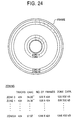
- Fig. 24 is a schematic representation of the disk 1 divided into 92 zones in the above-described way as shown in Figs. 12 to 15.
- the disk 1 is driven at a fixed (same) angular velocity in all of these 92 zones, it is also possible to form bands over a plurality of zones and to drive the disk 1 at an angular velocity different for each band though driven at a fixed angular velocity within the band.
- v3 (rn / r3) ⁇ v1
- the band is divided at the intermediate radius r3 of the radius r0 of the innermost region and the radius Rn of the outermost region.
- the widths of changes in the linear velocity in the two bands can also be made the same.
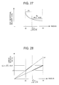
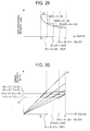
- Figs. 29 and 30 in correspondence with Figs. 25 and 26, show a case in which bands are formed by equally dividing the range of radiuses r0 to Rn into 4 at radiuses r8, r9 and r10.
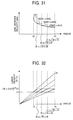
- Figs. 31 and 32 in correspondence with Figs. 27 and 28, show a case in which a band is divided at radiuses r5, r6 and r7 so that the widths of changes in the linear velocity in each band become the same.
- v5 (r5 / r0)
- v1 (r0 ⁇ r6) 1/2
- v1 ((r0 ⁇ rn) 1/2 / r0) 1/2
- v1 (rn / r0) 1/4 v1
- the rotational velocity is set to R1.
- the rotational velocity is set to R5.
- the rotational velocity is set to R6.
- the rotational velocity is set to R7.
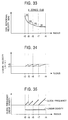
- the clock frequency is fixed within each zone as described above, but the clock frequency is switched for each zone, and in each band, the clock frequency increases more sequentially in the zones of the outer regions than in the zones of the inner regions.
- the clock frequencies at the beginning points of each band at radiuses r0, r5, r6 and r7 are the same; however, since the widths (number of tracks) of each band differ, the value of the clock frequency at the termination point of each band is greater in the case of the bands of a more outer region.
- the linear density is smaller in the outer regions than in the inner regions; in every zone of every band, the change width is fixed.
- step S11 when a track number is read from the wobble address, in step S12 the zone and the band of the read track number are read from the ROM 47. Then, a check is made in step S13 to determine if the zone of the read track number is a new zone. When it is determined that it is a new zone, the process proceeds to step S14 where a process for changing the frequency-dividing ratio of the PLL circuit 41 is performed.
- step S15 a check is made in step S15 to determine if the band of the track number read in step S12 is a new band.
- the process proceeds to step S16 where the control circuit 38 causes the rotational velocity of the spindle motor 31 to change to an angular velocity corresponding to the new band.
- step S13 When it is determined in step S13 that the zone is not a new zone, the process of steps S14 to S16 is skipped. Further, when it is determined in step S15 that the band of the read track number is not a new band, the process of steps S16 is skipped.
- each zone divided into 92 zones 0 to 91 is grouped into bands so that the change widths of the linear velocity in each band are fixed as shown in Figs. 31 and 32, and each parameter is as shown in Figs. 37 to 40.
- data in the seven columns on the left side is the same as the case in Figs. 12 to 15, and data in the three columns on the right side respectively indicates the rotational velocity in each zone, the minimum linear velocity in each zone, and the maximum linear velocity in each zone.
- zones 0 to 15 are assumed to be a first band
- zones 16 to 35 are assumed to be a second band
- zones 36 to 60 are assumed to be a third band
- zones 61 to 92 are assumed to be a fourth band.
- the length (number of bytes) of each area in the above-described embodiment is an example, and it is possible to appropriately set predetermined values.
- data is divided into blocks of a predetermined length, and a front link area and a back link area are respectively added before and after the obtained block in order to form a recording and reproduction unit.
- An address prerecorded on a rewritable-type disk is detected, and the recording and reproduction unit is recorded on a predetermined area of the rewritable-type disk on the basis of the detected address. Therefore, the position of a synchronization signal recorded on the rewritable-type disk is changed for each incidence of recording. Thus, it becomes possible to prevent thermal stress from accumulating on a recording medium of a rewritable-type disk.
- a recording and reproduction unit formed in such a way that a front link area and a back link area are added respectively before and after data divided into a predetermined length is recorded thereon, and the recording and reproduction unit is recorded in such a way that the lengths of the front link area and the back link area are changed randomly so that the recording and reproduction unit has a fixed length. Therefore, it becomes possible to protect a recording medium from thermal stress.
Abstract
Description
- The present invention relates to a recording and reproduction apparatus and method, and a disk. More particularly, the present invention relates to a recording and reproduction apparatus and method, and a disk, in which thermal stress is prevented from accumulating on a recording medium when data is repeatedly recorded on a disk.
- A conventional recording apparatus records data by modulating the intensity of a laser beam on the basis of data to be recorded and radiating it onto a disk, and causing a physical change in a recording medium.
- In such conventional recording apparatuses, data is recorded on the basis of address information prerecorded on a disk. Therefore, when data is recorded with specific address information being specified, the area where the data is recorded is predetermined on the disk.
- For example, it is known in a rewritable-type disk that, when a recording laser beam is repeatedly radiated onto the same area, thermal stress is accumulated on a recording medium. As a result, accurately recording data becomes difficult.
- When data is recorded on a disk, it is necessary to record a signal for synchronization (hereinafter abbreviated as a synchronization signal) together with the data to be recorded in order to synchronize signals during reproduction. Since information (content) in such a synchronization signal is often determined according to the position (address) on the disk, a specific synchronization signal is provided for a predetermined address.
- Therefore, when data is repeatedly recorded (overwritten) on a rewritable-type disk, the same synchronization signal is repeatedly written on the same portion of the disk. As a result, there is a problem in that thermal stress accumulates on that portion of the recording medium, and it becomes difficult to accurately reproduce a synchronization signal.
- Accordingly, in order to solve such problems, a recording method for randomly changing the recording start point of recording data is disclosed in Japanese Patent Publication No. 8-10489. However, such a method has problems in that since data recorded on a disk is noncontinuous, it is difficult to provide recording timing during recording.
- The present invention has been achieved in view of such circumstances. The present invention makes it possible to prevent thermal stress from accumulating on a recording medium even when overwriting is performed on a rewritable-type disk and to record data continuously.
- The recording and reproduction apparatus of
claim 1 comprises: division means for dividing data into blocks of a predetermined length; recording and reproduction unit formation means for forming a recording and reproduction unit by adding a front link area and a back link area of a predetermined length before and after the block, respectively; address detection means for detecting an address prerecorded on the rewritable-type disk; and recording means for recording the recording and reproduction unit on a predetermined area of the rewritable-type disk on the basis of an output from the address detection means. - The recording and reproduction method of
claim 10 comprises: a dividing step for dividing data into blocks of a predetermined length; a recording and reproduction unit formation step for forming a recording and reproduction unit by adding a front link area of a predetermined length and a back link area of a predetermined length before and after the block, respectively; an address detection step for detecting an address prerecorded on the rewritable-type disk; and a recording step for recording the recording and reproduction unit on a predetermined area of the rewritable-type disk on the basis of the address detected in the address detection step. - In the disk of
claim 11, a recording and reproduction unit formed in such a way that a front link area and a back link area are respectively added before and after data divided into a predetermined length is recorded thereon. The lengths of the front link area and the back link area are randomly changed so that the recording and reproduction unit has a fixed length. - In the recording and reproduction apparatus of
claim 1, the division means divides data into blocks of a predetermined length, the recording and reproduction unit formation means forms a recording and reproduction unit by respectively adding a front link area and a back link area of a predetermined length before and after the block, the address detection means detects an address prerecorded on a rewritable-type disk, and the recording means records the recording and reproduction unit on a predetermined area of the rewritable-type disk on the basis of an output from the address detection means. For example, data to be recorded is divided into blocks of a predetermined length by the division means, a front link area and a back link area are respectively added before and after the block, and a recording and reproduction unit to which the front and back link areas are added is recorded on a disk on the basis of the address detected by the address detection means. - In the recording and reproduction method of
claim 10, data is divided into blocks of a predetermined length in the division step, a recording and reproduction unit is formed by adding a front link area and a back link area of a predetermined length before and after the block, respectively, in the recording and reproduction unit formation step, the address prerecorded on a rewritable-type disk is detected in an address detection step, and the recording and reproduction unit is recorded on a predetermined area of the rewritable-type disk on the basis of an output from the address detection step in the recording step. For example, data to be recorded is divided into blocks of a predetermined length in the division step, a front link area and a back link area are added respectively before and after the block, and a recording and reproduction unit to which the front link area and the back link area are added is recorded on a disk on the basis of the address detected in the address detection step. - In the disk of
claim 11, a recording and reproduction unit formed in such a way that a front link area and a back link area are respectively added before and after data divided into a predetermined length is recorded thereon, and the recording and reproduction unit is recorded with the lengths of the front link area and the back link area randomly changed so that the recording and reproduction unit has a fixed length. For example, a recording and reproduction unit is formed in such a way that a front link area and a back link area whose lengths are randomly changed are respectively added before and after the data divided into a predetermined length, and the recording and reproduction unit is recorded. - The above and further objects, aspects and novel features of the invention will become more apparent from the following detailed description when read in connection with the accompanying drawings.
-
- Figs. 1A and 1B show a state in which a disk of the present invention is wobbled;
- Fig. 2 shows an example of the structure of a wobbling address frame;
- Fig. 3 shows an example of the construction of a wobbling signal generation circuit;
- Fig. 4 shows an example of a biphase signal output from a
biphase modulation circuit 13 of Fig. 3; - Fig. 5 shows another example of the biphase signal output from the
biphase modulation circuit 13 of Fig. 3; - Fig. 6 shows frequency modulation performed by an
FM modulation circuit 15 of Fig. 3; - Fig. 7 shows a frequency-modulated wave output from the
FM modulation circuit 15 of Fig. 3; - Fig. 8 shows an example of the construction of a recording apparatus for manufacturing a
disk 1 having a pre-groove; - Figs. 9A, 9B, 9C and 9D show the operation of a
synthesis circuit 22 of Fig. 8; - Fig. 10 is a block diagram illustrating an example of the construction of an optical disk recording and reproduction apparatus in which a recording and reproduction apparatus of the present invention is applied;
- Fig. 11 shows zones in a disk;
- Fig. 12 shows parameters of each zone;
- Fig. 13 shows parameters of each zone;
- Fig. 14 shows parameters of each zone;
- Fig. 15 shows parameters of each zone;
- Fig. 16 is a flowchart illustrating a clock switching process in the embodiment in Fig. 10;
- Fig. 17 shows the format of data for one sector;
- Fig. 18 shows the structure of data of 32 kilobytes;
- Fig. 19 shows a state in which an outer code of Fig; 18 is interleaved;
- Fig. 20 shows the structure of data of 32-kilobyte blocks;
- Fig. 21 shows the frames of a ROM disk and a RAM disk and an example of the structure of a frame synchronization signal;
- Fig. 22 shows an example of the frame synchronization signal shown in Fig. 21;
- Fig. 23 shows an example of the structure of a link area;
- Fig. 24 shows a state in which a disk is divided into 92 zones;
- Fig. 25 shows a disk rotational velocity when the disk is divided into two bands;
- Fig. 26 shows a linear velocity when the disk is divided into two bands;
- Fig. 27 shows a disk rotational velocity when the disk is divided into two bands;
- Fig. 28 shows a linear velocity when the disk is divided into two bands;
- Fig. 29 shows a disk rotational velocity when the disk is divided into four bands;
- Fig. 30 shows a linear velocity when the disk is divided into four bands;
- Fig. 31 shows a disk rotational velocity when the disk is divided into four bands;
- Fig. 32 shows a linear velocity when the disk is divided into four bands;
- Fig. 33 shows a disk rotational velocity when the disk is divided into four bands;
- Fig. 34 shows a linear velocity when the disk is divided into four bands;
- Fig. 35 shows a linear velocity and a clock frequency when the disk is divided into four bands;
- Fig. 36 is a flowchart illustrating clock switching and rotation control processes when a band is divided;
- Fig. 37 shows parameters when the disk is divided into four bands;
- Fig. 38 shows parameters when the disk is divided into four bands;
- Fig. 39 shows parameters when the disk is divided into four bands; and
- Fig. 40 shows parameters when the disk is divided into four bands.
- Figs. 1A and 1B show an example of the construction of an optical disk in which a disk of the present invention is applied. As shown in the figure, a
pre-groove 2 is formed beforehand in a spiral shape from the inner region toward the outer region in a disk (optical disk) 1. Of course, thispre-groove 2 may be formed in a concentric shape. - Further, as is shown by a portion of the pre-groove 2 exploded in Fig. 1B, the left and right side walls of the pre-groove 2 are wobbled on the basis of address information and are snaked in accordance with a frequency-modulated wave. One track has a plurality of wobbling address frames.
- Fig. 2 shows the structure (format) of a wobbling address frame. As shown in the figure, the wobbling address frame is formed of 48 bits, with the beginning 4 bits being a synchronization signal (Sync) indicating the start of a rewritable-type disk. The next 4 bits are made into a layer (Layer) indicating which layer from among a plurality of recording layers. The next 20 bits are made a track address (track number). Further, the next 4 bits indicate the frame number of the address frame. The subsequent 14 bits are made an error detection code (CRC), and an error detection code for data such that a synchronization signal (Sync) is excluded is recorded. The last 2 bits (Reserved) are kept in reserve for future use.
- The wobbling address frame is recorded in a CAV disk shape whose rotational angular velocity is fixed, for example, for an amount of 8 address frames per one track (one rotation). Therefore, as frame numbers in Fig. 2, for example, values from 0 to 7 are recorded.
- Fig. 3 shows an example of the construction of a wobbling signal generation circuit which generates a wobbling signal for wobbling the pre-groove 2 on the basis of the address frame of the format shown in Fig. 2. A
generation circuit 11 generates a signal having a frequency of 115.2 kHz. The signal generated from thegeneration circuit 11 is supplied to adivision circuit 12 whereby the signal is divided by a value 7.5, and is supplied as a biphase clock signal having a frequency of 15.36 kHz to abiphase modulation circuit 13. ADIP (Address In Pre-groove) data of a frame format shown in Fig. 2 is further supplied to thebiphase modulation circuit 13. - The
biphase modulation circuit 13 biphase-modulates a biphase clock supplied from thedivision circuit 12 by ADIP data (address data) supplied from a circuit (not shown) and outputs a biphase signal to anFM modulation circuit 15. A carrier having a frequency of 57.6 kHz obtained by dividing a signal of 115.2 kHz generated by thegeneration circuit 11 with avalue 2 by means of adivider 14 is further input to theFM modulation circuit 15. TheFM modulation circuit 15 frequency-modulates the carrier input from thedivider 14 by a biphase signal input from thebiphase modulation circuit 13 and outputs a frequency-modulated signal obtained thereby. The left and right side walls of thepre-groove 2 of thedisk 1 are formed (wobbled) in accordance with this frequency-modulated signal. - Figs. 4 and 5 show examples of a biphase signal output from the
biphase modulation circuit 13. In this embodiment, when the leading bit is 0, as shown in Fig. 4, "11101000" is used as a synchronization pattern (SYNC), and when the leading bit is 1, as shown in Fig. 5, "00010111" in a phase opposite to the case shown in Fig. 4 is used. SYNC is made a unique pattern as an exception to the rule which does not appear in the modulation. - "0" of the data bits (Data Bits) of the address data (ADIP data) is biphase-modulated and converted into channel bits (Channel Bits) of "11" (when the previous channel bit is 0) or "00" (when the previous channel bit is 1). Further, "1" is converted into channel bits of "10" (when the previous channel bit is 0) or "01" (when the previous channel bit is 1). Which of the two patterns this is converted into depends upon the previous code. That is, the "Wave Form" in Figs. 4 and 5 is such that patterns of 1,0 of channel bits are expressed with 1 being a high level and 0 being a low level. Any one of the two patterns is selected so that this waveform continues.
- The
FM modulation circuit 15 frequency-modulates a carrier supplied from thedivider 14 as shown in Fig. 6 in accordance with the biphase signal shown in Fig. 4 or 5. - That is, when the channel bit data (biphase signal) is 0, the
FM modulation circuit 15 outputs a carrier of 3.5 waves in a period corresponding to the length of half of one data bit. This carrier of 3.5 waves is a carrier which begins from a positive half wave or a negative half wave. - In comparison, when the channel bit data (biphase signal) is 1, a carrier of 4 waves is output in a period corresponding to the length of half of one data bit. This carrier of 4 waves also is a carrier which begins from a positive half wave or a negative half wave.
- Therefore, when channel data bits 00 are input in correspondence with
data 0, theFM modulation circuit 15 outputs a frequency-modulated wave of 7 waves (= 3.5 + 3.5) in a period corresponding to the length of the data bits, and outputs a frequency-modulated wave of 8 waves (= 4 + 4) whenchannel data bits 11 are input. Further, whenchannel data bits data 1, a frequency-modulated wave of 7.5 waves (= 4 + 3.5 = 3.5 + 4) is output. - The carrier of 57.6 kHz input to the
FM modulation circuit 15 corresponds to a 7.5 wave. In correspondence with data, theFM modulation circuit 15 generates this carrier of 7.5 waves, or a frequency-modulated wave of 7 or 8 waves such that the carrier of 7.5 waves is shifted by ± 6.67% (= 0.5/7.5). - As described above, regarding carriers which begin from a positive half wave and a negative half wave, corresponding to channel
data - Fig. 7 shows an example of a frequency-modulated wave output in this way from the
FM modulation circuit 15. In this example, the first data bit is made 0, and its channel data bits are made 00. With respect to the beginningchannel data bit 0, a carrier of 3.5 waves which begins from a positive half wave from the starting point is selected. As a result, the termination point of the carrier terminates at a positive half wave. Therefore, with respect to the next channel data bit 0, a 3.5 wave which begins from a negative half wave is selected, and thus a frequency-modulated wave of a total of 7 waves is formed with respect todata bit 0. - This
data bit 0 is followed by data bit 1 (channel bit 10). Since the 3.5 waves of the channel data bit corresponding to theprevious data bit 0 terminate at a negative half wave, a carrier of 4 waves of the beginning channel data bit 1 corresponding todata bit 1, which begins from a positive half wave, is selected. Since the 4 waves of the channel data bit 1 terminate at a negative half wave, the 4 waves of the next channel data bit 0, which begin from a positive half wave, are selected. - Hereinafter, in a similar manner, carriers of 7.5 waves, 8 waves and 7 waves, in correspondence with data bit 1 (channel data bit 10), data bit 0 (channel data bit 11), and data bit 0 (channel data bit 00), are formed in such a manner as to be continuous at the boundary portions (the beginning point and the termination point) of the data bits and are output.
- As shown in Fig. 7, in this embodiment, the length of the channel bits is made an integral multiple of 1/2 of the wavelength of the carrier in the case of 7, 7.5 or 8 waves. That is, the length of the channel bits is made 7
times 1/2 of the wavelength of the carrier (frequency-modulated wave) of 7 waves, and is made 8times 1/2 of the wavelength of the carrier (frequency-modulated wave) of 8 waves. Further, the length of the channel bits is made 7times 1/2 of 7.5 waves (when the channel bit is 0), and is made 8 times thereof (when the channel bit is 1). - Furthermore, in this embodiment, the boundary portion (the beginning point or the termination point) of the channel bits which are biphase-modulated is made a zero-cross point of the frequency-modulated wave. As a result, the phases of the address data (channel bit data) and the frequency-modulated wave coincide with each other, and the identification of the boundary portion of the bits is easy, making it possible to prevent erroneous detection of the address data bits. As a result, it becomes easy to accurately reproduce address information.
- Further, in this embodiment, the boundary portions (the beginning point and the termination point) of the data bits are made to correspond to the edges (the zero-cross points) of the frequency-modulated wave. As a result, it is also possible to generate a clock with the edge of the frequency-modulated wave as a reference. In this embodiment, however, as will be described later with reference to Figs. 9A to 9D, a clock is generated with a clock synchronization mark as a reference.
- Fig. 8 shows an example of the construction of a recording apparatus (disk formation apparatus) for manufacturing a
disk 1 having a pre-groove. A wobblingsignal generation circuit 21 has the construction shown in Fig. 3 and supplies a frequency-modulated signal output from theFM modulation circuit 15 to asynthesis circuit 22. A marksignal generation circuit 23 generates a clock synchronization mark signal at a predetermined timing and outputs it to thesynthesis circuit 22. Thesynthesis circuit 22 synthesizes a frequency-modulated signal output from the wobblingsignal generation circuit 21 and a clock synchronization mark signal output from the marksignal generation circuit 23 and outputs the result to arecording circuit 24. - When a clock synchronization mark signal is supplied, the
synthesis circuit 22 synthesizes the clock synchronization mark (Fine Clock Mark) onto a carrier supplied from the wobblingsignal generation circuit 21, as shown in Figs. 9A to 9D. When modulation of recording and reproduction data is made EFM (Eight to Fourteen Modulation: (8 - 14) modulation) + for DVD or the like, the clock synchronization mark is made a length from 6 to 14T (T is the length of a bit cell). - That is, as shown in Figs. 9A to 9D, when the channel bit data is 00 (data 0), 11 (data 0), 10 (data 1) or 01 (data 1), a clock synchronization mark of a frequency higher than the modulation frequency (57.6 kHz) of the address information is synthesized at the zero-cross point of the carrier of the respective data center (the switching point of the channel bits). This clock synchronization mark is recorded on every data bit or every predetermined number of data bits.
- Insertion of a clock synchronization mark at the zero-cross point of the wobbling frequency-modulated wave corresponding to the center (switching point of the channel data bits) of the address data bits as described above reduces amplitude variations of the clock synchronization mark, making it easy to detect the clock synchronization mark.
- That is, in the
FM modulation circuit 15, when the channel data bit is 0, frequency modulation is performed so as to shift the frequency, for example, by -5% from the center frequency, and when the channel data bit is 1, frequency modulation is performed so as to shift the frequency, for example, by +5% from the center frequency, the data bits or the boundary portion of the channel data bits and the zero-cross point of the frequency-modulated wave do not coincide with each other, and thus it is likely to erroneously detect the channel data bits (or the data bits). Further, the insertion position of the clock synchronization mark is not necessarily a zero-cross point and is superimposed onto a point of the frequency-modulated wave having a predetermined amplitude value. As a result, the level of the clock synchronization mark is increased or decreased by an amount corresponding to the amplitude value, and detection of the clock synchronization mark becomes difficult. According to this embodiment, since the clock synchronization mark is always placed at the zero-cross point of the frequency-modulated wave, the detection (identification from the frequency-modulated wave) of the clock synchronization mark is made easy. - The
recording circuit 24 controls anoptical head 25 in accordance with a signal supplied from thesynthesis circuit 22 in order to generate laser light for forming a pre-groove (including a clock synchronization mark) on anoriginal disk 26. Aspindle motor 27 causes theoriginal disk 26 to rotate at a fixed angular velocity (CAV). - More specifically, the frequency-modulated wave generated by the wobbling
signal generation circuit 21 is synthesized, in thesynthesis circuit 22, onto the clock synchronization mark signal output from the marksignal generation circuit 23, and is input to therecording circuit 24. Therecording circuit 24 controls theoptical head 25 in accordance with the signal input from thesynthesis circuit 22 in order to generate laser light. The laser light generated from theoptical head 25 is radiated onto theoriginal disk 26 rotated at a fixed angular velocity by thespindle motor 27. - The
original disk 26 is developed, a stamper is made from thisoriginal disk 26, anddisks 1 are formed as a number of replicas from the stamper. This makes it possible to obtain adisk 1 on which apre-groove 2 having the above-described clock synchronization mark is formed. - Fig. 10 shows an example of the construction of an optical disk recording and reproduction apparatus for recording data to or reproducing data from the
disk 1 obtained in this way. Aspindle motor 31 causes thedisk 1 to rotate at a predetermined angular velocity. An optical head 32 (recording means, recording step) radiates laser light onto thedisk 1 in order to record data onto thedisk 1 and reproduce data from the light reflected therefrom. A recording and reproducing circuit 33 (recording and reproduction unit formation means, recording and reproduction unit formation step, addition means, addition step, second addition means) temporarily stores recording data input from an apparatus (not shown) in a memory 34 (division means, division step), reads one cluster of data when this one cluster of data (or may also be one sector of data), which is a recording unit, is stored in thememory 34, and, for example, modulates the data by a predetermined method and then outputs the modulated data to theoptical head 32. Further, the recording and reproducingcircuit 33 appropriately demodulates the data input from theoptical head 32 and outputs the demodulated data to an apparatus (not shown). - The recording and reproducing
circuit 33, as will be described later, adds a front link area and a back link area to the recording data and adds a synchronization signal to these link areas, and then outputs the result. - An address generation and reading circuit 35 (address detection means, address detection step) generates a data address (sector address) (will be described later with reference to Fig. 17) to be recorded within the track (pre-groove 2) under control from a
control circuit 38 and outputs the data address to the recording and reproducingcircuit 33. The recording and reproducingcircuit 33 adds this address to the recording data supplied from the apparatus (not shown) and outputs the data to theoptical head 32. Further, when address data is contained within the reproduction data which is reproduced from the tracks of thedisk 1 by theoptical head 32, the recording and reproducingcircuit 33 separates this address data and outputs it to the address generation and readingcircuit 35. The address generation and readingcircuit 35 outputs the read address to thecontrol circuit 38. - Further, a
mark detection circuit 36 detects components corresponding to the clock synchronization mark from an RF signal reproduced and output by theoptical head 32. A frameaddress detection circuit 37 reads address information (the track number and the frame number in Fig. 2) contained in the wobbling signal from the RF signal output from theoptical head 32 and supplies the address information to acluster counter 46 and thecontrol circuit 38. - A mark
cycle detection circuit 40 determines the periodicity of detected pulses which are output when themark detection circuit 36 detects a clock synchronization mark. That is, since the clock synchronization mark is generated at a fixed cycle, a check is made to determine if the detected pulses input from themark detection circuit 36 are detected pulses generated at this current fixed cycle. If the pulses are detected pulses generated at this fixed cycle, pulses which are synchronized with the detected pulses are generated, and output to aphase comparator 42 of aPLL circuit 41 of a latter stage. Further, in a case in which detected pulses are not input at a fixed cycle, the markcycle detection circuit 40 generates a pseudo pulse at a predetermined timing so that thePLL circuit 41 of the latter stage does not lock to an incorrect phase. - The
PLL circuit 41 has, in addition to thephase comparator 42, a low-pass filter (LPF) 43, a voltage control oscillator (VCO) 44, and afrequency divider 45. Thephase comparator 42 compares the phase of an input from the markcycle detection circuit 40 with that of an input from thefrequency divider 45 and outputs a difference between the phases. The low-pass filter 43 smooths the phase difference signal output from thephase comparator 42 and outputs the signal to theVCO 44. TheVCO 44 generates a clock with a phase corresponding to the output from the low-pass filter 43 and outputs the clock to thefrequency divider 45. Thefrequency divider 45 frequency-divides the clock input from theVCO 44 by a predetermined value (a value specified by the control circuit 38) and outputs the frequency-divided result to thephase comparator 42. - The clock output from the
VCO 44 is supplied to each circuit and also to thecluster counter 46. The cluster counter 46 counts the number of clocks output from theVCO 44 using the frame address supplied from the frameaddress detection circuit 37 as a reference, generates a cluster start pulse when the counted value reaches a predetermined value (a value corresponding to the length of one cluster) which is set previously, and outputs the value to thecontrol circuit 38. - A
thread motor 39, which is controlled by thecontrol circuit 38, transports theoptical head 32 to a predetermined track position of thedisk 1. Further, thecontrol circuit 38 controls thespindle motor 31 so as to rotate thedisk 1 at a predetermined angular velocity (CAV). - A
ROM 47 has stored therein, a table which defines the correspondence relationship between track numbers (Fig. 2) in the address frame and zones which separate the data recording areas of thedisk 1, and, as required, a table which defines the relationship between zones and a band (the details of which will be described later) to which a zone corresponds. - More specifically, as in the
disk 1 shown in Fig. 11, thecontrol circuit 38 records or reproduces data to and from a plurality of divided zones (in this embodiment, m + 2 zones of the 0-th zone to the m + 1 zone). When the number of data frames (unlike the address frame described with reference to Fig. 2, this data frame is a unit of blocks of data) per one track of the 0-th zone is set to n, in the next 1st zone, the number of data frames per one track is set to n + 8. Hereinafter, in a similar manner, in the zone of a more outer region, the number of data frames increases by 8 than an adjacent zone of the inner region. In the m + 1 zone of the outermost region, the number of data frames reaches
- A change is made to the 1st zone from the radius position at which a capacity of n + 8 frames can be obtained at the same linear density as the innermost-region linear density of the 0-th zone. Hereinafter, in a similar manner, in the m-th zone, the m-th zone is formed from the radius position at which a capacity of

- If, for example, the range in which the radius of the
disk 1 is from 24 to 58 mm is made a recording and reproducing area, the track pitch is 0.87 µm, and the linear density is 0.38 µm/bit, the recording and reproducing area is divided into 92 zones, as shown in Figs. 12 to 15. In the 0-th zone in which the disk radius is 24 mm, there are 520 frames per one track (one rotation). As the zone is incremented by 1, there is an increase of 8 frames per one track. - As will be described later, in this embodiment, since one sector is formed of 26 frames (data frames), the number (= 8) of frames which is incremented for each zone is set to a value smaller than this number (= 26) of frames which constitute one sector. This makes it possible to form zones in smaller units and to increase the capacity of the
disk 1. This method is called zone CLD (Constant Linear Density). - In Figs. 12 to 15, data of each column respectively indicate the zone number, the radius, the number of frames per one track, the number of tracks per one zone, the number (number of clusters) of recording and reproduction units (blocks) per one zone, the minimum linear density within the zone, the capacity of the zone, the rotational velocity of the zone, the minimum linear velocity of the zone, and the maximum linear velocity of the zone. The rotational velocity indicates the number of rotations per minute when the data transfer rate is set at 11.08 Mbps.
- In this embodiment, the number of tracks in each zone is fixed to 424. This number of tracks is made the same value as the number (the number of frames of an ECC block) (will be described later with reference to Fig. 20) of frames in one recording and reproduction unit.
- Although in this embodiment the number of tracks in each zone is made one times the number of data frames (424 frames) which constitute the recording and reproduction unit, the number may be an integral multiple thereof. This prevents excess data frames from occurring, and an integral number of recording and reproduction units (blocks) are placed in each zone, making it possible to improve zoning efficiency. As a result, it is possible to obtain a capacity which is larger than zone CAV and close to zone CLV, though smaller than zone CLV.
- Further, as described above, by performing zoning close to CLV, changes in clock frequency in one zone and the next zone become small. Thus, even when reproduction is performed by a reproduction apparatus exclusively used for CLV, extraction of a clock is made possible from zone from zone where the clock frequency changes, and thus reproduction can be made continuously from zone from zone.
- Next, the operation of the embodiment shown in Fig. 10 will be described. Here, the operation during recording of data will be described. The
optical head 32 radiates laser light onto theoptical disk 1 and outputs an RF signal obtained from the light reflected therefrom. The frameaddress detection circuit 37 reads wobbling information (address information) from the RF signal, and outputs the read result to thecontrol circuit 38 and also to thecluster counter 46. Further, this wobbling information is input to themark detecting circuit 36 whereby a clock synchronization mark is detected and supplied to the markcycle detection circuit 40. - The mark
cycle detection circuit 40 determines the periodicity of the clock synchronization mark, generates a predetermined pulse corresponding thereto, and outputs the pulse to thePLL circuit 41. ThePLL circuit 41 generates a clock (recording clock) which is synchronized with this pulse and supplies the clock to thecluster counter 46. - The
control circuit 38 is capable of detecting the position of a reference clock synchronization mark in one track (one rotation) from the frame address (frame number) supplied from the frameaddress detection circuit 37. For example, with the clock synchronization mark detected at the beginning of a frame (address frame) offrame number 0 as a reference, it becomes possible to access any desired position (any desired position during one rotation) on the track on the basis of the count value of the recording clock. - In the above-described way, when an access to any desired position on the track is made, it is further necessary to determine to which zone that access point belongs and to cause the
VCO 44 to generate a clock of a frequency corresponding to the zone. Therefore, thecontrol circuit 38 further performs a clock switching process such as that shown in the flowchart of Fig. 16. - More specifically, initially, in step S1, the
control circuit 38 reads the track number from the frame address of the access point output from the frameaddress detection circuit 37. Then, in step S2, a zone corresponding to the track number read in step S1 is read from the table stored in theROM 47. As described above, the table in theROM 47 has prestored therein information on to which of the 0-th to 92-th zones the track of each number belongs. - Therefore, in step S3, a check is made to determine if the track number just read indicates a new zone different from the zone which has been accessed up until then. When it is determined that the zone is a new zone, the process proceeds to step S4 where the
control circuit 38 controls thefrequency divider 45 in order to set a frequency-dividing ratio corresponding to the new zone. As a result, a recording clock of a frequency different for each zone is output from theVCO 44. - Meanwhile, when it is determined in step S3 that the current zone is not a new zone, the process in
step 4 is skipped. That is, the frequency-dividing ratio is kept as it is without being changed. - Next, the format of recording data will be described. In this embodiment, as described above, data is recorded in units of one cluster (32 kilobytes), and this cluster is structured as described below.
- That is, data of 2 kilobytes (2048 bytes) is extracted as data for one sector, and an overhead of 16 bytes is added thereto as shown in Fig. 17. This overhead contains a sector address (address generated or read by the address generation and reading
circuit 35 in Fig. 10) and an error detection code for error detection. - This data of a total of 2064 (2048 + 16) bytes is formed into data of 12 × 172 (= 2064) bytes, as shown in Fig. 18. Then, 16 of these data for one sector are collected and formed into data of 192 (= 12 × 16) × 172 bytes. For this data of 192 × 172 bytes, a 10-byte inner code (PI) and a 16-byte outer code (PO) are added as parities to each byte in the horizontal and vertical directions.
- Further, of the data which is blocked to 208 (= 192 + 16) × 182 (= 172 + 10) bytes, the outer code (PO) of the 16 × 182 bytes is divided into 16 data of 1 × 182 bytes. As shown in Fig. 19, the data is added one at a time to below the 16 sector data of
number 0 tonumber 15 of 12 × 182 bytes and is interleaved. Then, data of 13 (= 12 + 1) × 182 bytes is assumed to be data of one sector. - Further, data of 208 × 182 bytes shown in Fig. 19, as shown in Fig. 20, is divided into two parts in the vertical direction, one frame is formed into data of 91 bytes, and thus the data is formed into data of 208 × 2 frames. Then, link data (data of the link area) of 4 × 2 frames is added (more precisely, as will be described later with reference to Fig. 23, a part of data for 8 frames is recorded onto the start of the cluster, and the remainder is recorded onto the end of the cluster) to the head of this data of 208 × 2 frames. A 2-byte frame synchronization signal (FS) is further added to the head of the 91-byte frame data. As a result, as shown in Fig. 20, data of one frame becomes data of a total of 93 bytes, and becomes data of blocks of a total of 212 (= 208 + 4) × (93 × 2) bytes (424 frames). This becomes data for one cluster (blocks as a recording unit). The size of the real data section such that the overhead portion is excluded becomes 32 kilobytes (= 2048 × 16 / 1024 kilobytes).
- That is, in this embodiment, one cluster is formed of 16 sectors and one sector is formed of 26 frames.
- Fig. 21 shows each frame of a ROM disk (read-only disk) and a RAM disk (rewritable-type disk), and the structure of a frame synchronization signal. In the ROM disk, one sector is formed of 13 rows of data, i.e., 26 frames. Further, frame synchronization signals SY0 to SY7 are added to the head of each frame.
- Further, in the case of the RAM disk, a link area of 8 frames is added followed by 13 rows of data, i.e., data of 26 frames, and then data of 26 frames is added. The structures of the frame synchronization signal of the data area of the RAM disk and the frame synchronization signal of the data area of the ROM disk are the same. In addition, the frame synchronization signal of the link area of the RAM disk is formed the same as the end portion of the frame synchronization signal of the data area. That is, SY1 to SY4 and SY7 of the link area are the same patterns as the 10-th to 13-th rows of the data area. With such a construction, it becomes possible to reproduce a RAM disk by a reproduction apparatus exclusively used for ROM disks.
- More specifically, a reproduction apparatus exclusively used for ROM disks is formed in such a way that, when 8 frame synchronization signals SY1, SY7, SY2, SY7, SY3, SY7, SY4, and SY7 stored in the 10-th to 13-th rows of the data blocks are detected, the reproduction apparatus recognizes the next data to be the beginning portion of a data block. Therefore, by storing these 8 frame synchronization signals in the link area, it is possible to cause the reproduction apparatus to recognize the beginning portion of the data area which follows the link area.
- Fig. 22 shows an example of the frame synchronization signals SY0 to SY7 shown in Fig. 21. Although a frame synchronization signal is 2-byte data, in this embodiment, data after conversion is shown in the channel bit data; therefore, the data length of each frame synchronization signal is 32 bits (4 bytes). For example, there are four types of
states 1 to 4 in SY0. When the signal is added to frame data (see Fig. 20) of 91 bytes, data of a state in which a DSV (Digital Sum Value) reaches a minimum is selected and is added as a frame synchronization signal. - Since such data is recorded on the
disk 1 in cluster units, a link area is formed between clusters, as shown in Fig. 23. - As shown in Fig. 23, a link area (Linking Frame) is formed of 8 frames and is inserted between data blocks of 32 kilobytes. Each RW unit (recording and reproduction unit) is formed of: slice/PLL data which is a front link area of a 32-kilobyte data block or link data, such as frame synchronization signals SY1 to SY7; a 32-kilobyte data block; a postamble which is a back link area of the 32-kilobyte data block; and a postguard.
- A slice is data for setting the time constant for binarizing reproduction data, and a PLL is data for reproducing a clock. Regarding the frame synchronization signals SY1 to SY7, any of
state 1 tostate 4 is selected and added thereto, as described above with reference to Fig. 22. - Data for adjusting the mark length of the last data and for returning the signal polarity is recorded in the postamble. The postguard is an area for absorbing recording jitter which occurs in response to decentering of the disk, recording sensitivity of the disk and the like. Further, the postguard prevents data from mutually interfering in the link area adjoining a link area to be recorded next even when the data recording start position is changed as will be described later. Furthermore, the postguard is recorded in such a manner as to overlap the next data by 8 bytes when there is no jitter and when a DPS (Data Position Shift) to be described later is 0 bytes.
- The synchronization signal (sync), which is 4-byte data, is a signal for synchronization. Further, the last 4 bytes are reserved for future use.
- In each RW unit (recording and reproduction unit), recording of information is started from the start point (Start Point), and recording is terminated when excess (overlap) of 8 bytes from the start point occurs. Further, during recording, the recording and reproducing
circuit 33 randomly selects any one of the values of 0 to 64 bytes and changes the recording position of the data of the link area and the 32-kilobyte data block data on the basis of the value of the selected DPS. - As shown in an exploded view in Fig. 23, when, for example, 0 bytes are selected as the DPS, a 14-byte link data is added before the first frame synchronization signal SY2 of the front link area, and 85-byte link data is added after the final frame synchronization signal SY7 of the back link area.
- Further, when 32 bytes are selected as the DPS, a 46-byte link data is added before the first frame synchronization signal SY2 of the front link area, and a 53-byte link data is added after the final frame synchronization signal SY7 of the back link area.
- In addition, when 64 bytes are selected as the DPS, 78-byte link data is added before the first frame synchronization signal SY2 of the front link area, and 21-byte link data is added after the final frame synchronization signal SY7 of the back link area.
- As described above, on the basis of the value of the DPS selected by the recording and reproducing
circuit 33, the positions at which the link data and the 32-kilobyte data blocks are recorded vary. Therefore, during recording on a phase-change disk, it is possible to prevent the same data (e.g., a frame synchronization signal, etc.) from being repeatedly recorded on the same portion of a disk. Further, in such a case, since the start point is fixed, it is possible to generate a recording timing in a manner similar to that done conventionally. - Fig. 24 is a schematic representation of the
disk 1 divided into 92 zones in the above-described way as shown in Figs. 12 to 15. Although in the above-described embodiment, in any zone of the respective 92 zones, thedisk 1 is driven at a fixed (same) angular velocity in all of these 92 zones, it is also possible to form bands over a plurality of zones and to drive thedisk 1 at an angular velocity different for each band though driven at a fixed angular velocity within the band. - For example, as shown in Figs. 25 and 26, when the range from the radius r0 of the innermost region to the radius rn of the outermost region is an area in which data is recorded and reproduced, the area is divided at the intermediate radius

disk 1 is rotated at a predetermined angular velocity. When the angular velocity (rotational velocity) at radius r0 is denoted as R1, an angular velocity R3 at radius r3 can be determined from the following equation since the angular velocity is inversely proportional to the radius:
- Further, as shown in Fig. 26, when a linear velocity at radius r0 is denoted as v1, a linear velocity v4 can be determined from the following equation since the linear velocity at radius r3 within the first band is inversely proportional to the radius:

- Further, since the linear velocity at radius r3 in the next band is v1, a linear velocity v3 at radius rn can be determined from the following equation:

- If the area is divided into bands in this way, since it is possible to make the rotational velocity slow in the case of the bands from radius r3 to radius rn than in the case of the bands from radius r0 to radius r3, it is possible to increase the recording capacity more than in the case of the normal zone CAV method.
- In the embodiment in Figs. 25 and 26, the band is divided at the intermediate radius r3 of the radius r0 of the innermost region and the radius Rn of the outermost region. As a result, the widths of the changes in the linear velocity of the two bands are different.
- Thus, as shown, for example, in Figs. 27 and 28, the widths of changes in the linear velocity in the two bands can also be made the same.
- More specifically, in this case, if the radius which divides the band is denoted as r2 and the linear velocity at the termination point of each band as v2, the following equations can be obtained from the relationship between the linear velocities:

- Therefore, the following equations can be obtained from the above-described equations:

- Further, if the rotational velocity in the bands from radius r0 to radius r2 is denoted as R1 and the rotational velocity from radius r2 to radius rn as R2, R2 can be determined from the following equation:

- As described above, if an area is divided into two bands at radius r2, the widths of the changes in the linear velocity in each band can be made the same.
- Although in the above-described embodiment the number of bands is 2, the number may also be 4. Figs. 29 and 30, in correspondence with Figs. 25 and 26, show a case in which bands are formed by equally dividing the range of radiuses r0 to Rn into 4 at radiuses r8, r9 and r10. Figs. 31 and 32, in correspondence with Figs. 27 and 28, show a case in which a band is divided at radiuses r5, r6 and r7 so that the widths of changes in the linear velocity in each band become the same.
- That is, in the embodiment shown in Figs. 29 and 30, since the range from radiuses r0 to Rn is equally divided into 4 at radiuses r8, r9 and r10, each radius is expressed by the following equations:

- Also, the rotational velocities R8, R9 and R10 of each band are expressed by the following equations, respectively:

- Further, the linear velocities v8, v9, v10 and v11 at the termination points of each band of radiuses r8, r9, r10 and rn can be determined by the following equations, respectively:

- On the other hand, in the embodiment in Figs. 31 and 32, the rotational velocities R5, R6 and R7 at radiuses r5 to r6, radiuses r6 to r7, and radiuses r7 to rn can be determined by the following equations, respectively:

- Further, as shown in Fig. 32, when the linear velocity at radiuses r5, r6, r7, and rn of the termination points of each band is denoted as v5, the following equation is satisfied:

- Therefore, the following equations are obtained:

- Further, the linear velocity v5 at each radius r5, r6, r7 and rn can be determined from the following equation:

- In the case of normal CAV disks, since the linear velocity at the position of radius Rn is vn, the change width consequently becomes vn - v1. In comparison, in the embodiment shown in Figs. 31 and 32, it is possible to suppress the above change width to a change width (change width of 1/4 or less of (vn - v1)) of v5 - v1.
- As described above, when the range of radiuses r0 to Rn is divided into 4 bands at radiuses r5, r6 and r7 so that the change width of the linear velocity becomes fixed, the rotational velocity of the disk, the linear velocity, as well as the linear density and the clock frequency, each vary as shown in Figs. 33 to 35.
- That is, in the bands from radiuses r0 to r5, the rotational velocity is set to R1. In the bands from radiuses r5 to r6, the rotational velocity is set to R5. In the bands from radiuses r6 to r7, the rotational velocity is set to R6. In the bands from radiuses r7 to rn, the rotational velocity is set to R7. Then, as shown in Fig. 34, in each band the linear velocity increases from v1 up to v5 from the innermost region toward the outermost region; however, the change width in each band is fixed.
- Further, as shown in Fig. 35, the clock frequency is fixed within each zone as described above, but the clock frequency is switched for each zone, and in each band, the clock frequency increases more sequentially in the zones of the outer regions than in the zones of the inner regions. The clock frequencies at the beginning points of each band at radiuses r0, r5, r6 and r7 are the same; however, since the widths (number of tracks) of each band differ, the value of the clock frequency at the termination point of each band is greater in the case of the bands of a more outer region.
- Further, in each zone, the linear density is smaller in the outer regions than in the inner regions; in every zone of every band, the change width is fixed.
- As described above, in a case in which a plurality of zones are collectively divided into a plurality of bands, the
control circuit 38 performs clock switching and rotation control processes shown in Fig. 36. The process from steps S11 to S14 is basically similar to the process from steps S1 to S4 in Fig. 16. That is, in step S11, when a track number is read from the wobble address, in step S12 the zone and the band of the read track number are read from theROM 47. Then, a check is made in step S13 to determine if the zone of the read track number is a new zone. When it is determined that it is a new zone, the process proceeds to step S14 where a process for changing the frequency-dividing ratio of thePLL circuit 41 is performed. Then, a check is made in step S15 to determine if the band of the track number read in step S12 is a new band. When it is determined that it is a new band, the process proceeds to step S16 where thecontrol circuit 38 causes the rotational velocity of thespindle motor 31 to change to an angular velocity corresponding to the new band. - When it is determined in step S13 that the zone is not a new zone, the process of steps S14 to S16 is skipped. Further, when it is determined in step S15 that the band of the read track number is not a new band, the process of steps S16 is skipped.
- As described above, as shown in Fig. 24, each zone divided into 92
zones 0 to 91 is grouped into bands so that the change widths of the linear velocity in each band are fixed as shown in Figs. 31 and 32, and each parameter is as shown in Figs. 37 to 40. In these figures, data in the seven columns on the left side is the same as the case in Figs. 12 to 15, and data in the three columns on the right side respectively indicates the rotational velocity in each zone, the minimum linear velocity in each zone, and the maximum linear velocity in each zone. As shown in these figures, in this embodiment,zones 0 to 15 are assumed to be a first band,zones 16 to 35 are assumed to be a second band,zones 36 to 60 are assumed to be a third band, andzones 61 to 92 are assumed to be a fourth band. - The length (number of bytes) of each area in the above-described embodiment is an example, and it is possible to appropriately set predetermined values.
- Also, when the present invention is applied to a phase-change-type disk, more satisfactory advantages can be obtained.
- As described above, according to the recording and reproduction apparatus of
claim 1 and the recording and reproduction method ofclaim 10, data is divided into blocks of a predetermined length, and a front link area and a back link area are respectively added before and after the obtained block in order to form a recording and reproduction unit. An address prerecorded on a rewritable-type disk is detected, and the recording and reproduction unit is recorded on a predetermined area of the rewritable-type disk on the basis of the detected address. Therefore, the position of a synchronization signal recorded on the rewritable-type disk is changed for each incidence of recording. Thus, it becomes possible to prevent thermal stress from accumulating on a recording medium of a rewritable-type disk. - According to the disk of
claim 11, a recording and reproduction unit formed in such a way that a front link area and a back link area are added respectively before and after data divided into a predetermined length is recorded thereon, and the recording and reproduction unit is recorded in such a way that the lengths of the front link area and the back link area are changed randomly so that the recording and reproduction unit has a fixed length. Therefore, it becomes possible to protect a recording medium from thermal stress. - Many different embodiments of the present invention may be constructed without departing from the spirit and scope of the present invention. It should be understood that the present invention is not limited to the specific embodiment described in this specification. To the contrary, the present invention is intended to cover various modifications and equivalent arrangements included within the spirit and scope of the invention as hereafter claimed. The scope of the following claims is to be accorded the broadest interpretation so as to encompass all such modifications, equivalent structures and functions.
Claims (15)
- A recording and reproduction apparatus for recording data to and reproducing data from a rewritable-type disk (1), comprising:division means for dividing data into blocks of a predetermined length;recording and reproduction unit formation means (33) for forming a recording and reproduction unit by adding a front link area and a back link area of a predetermined length before and after said block, respectively;address detection means (37) for detecting an address prerecorded on said rewritable-type disk; andrecording means (32) for recording said recording and reproduction unit on a predetermined area of said rewritable-type disk (1) on the basis of an output from said address detection means.
- A recording and reproduction apparatus according to claim 1, wherein said rewritable-type disk is a phase-change-type disk (1).
- A recording and reproduction apparatus according to claims 1 or 2, wherein said recording and reproduction unit formation means (33) randomly changes the length of said front link area and said back link area so that the length of said recording and reproduction unit is fixed.
- A recording and reproduction apparatus according to anyone of the preceding claims, wherein said recording means (32) records a first and a second recording and reproduction unit so that a part of said back link area of said first recording and reproduction unit and a part of said front link area of said second recording and reproduction unit overlap.
- A recording and reproduction apparatus according to claim 4, wherein said recording means (32) records a first and a second recording and reproduction unit so that the final synchronization signal of said back link area of said first recording and reproduction unit and the first synchronization signal of said front link area of said second recording and reproduction unit do not overlap.
- A recording and reproduction apparatus according to anyone of the preceding claims, further comprising: addition means for adding a synchronization signal to said data, wherein a synchronization signal added by said addition means is formed similar to a synchronization signal recorded on a read-only disk.
- A recording and reproduction apparatus according to claim 6, further comprising: second addition means for adding a synchronization signal to said front link area or said back link area,
wherein a synchronization signal added by said second addition means is formed similar to the end portion of the synchronization signal added by said addition means. - A recording and reproduction apparatus according to anyone of the preceding claims, wherein said recording and reproduction unit formation means (33) forms, in said back link area, a postguard area for preventing data from mutually interfering.
- A recording and reproduction apparatus according to anyone of the preceding claims, wherein the length of said back link area is made to be one or more data frames.
- A recording and reproduction method for recording data to and reproducing data from a rewritable-type disk, comprising:a dividing step for dividing data into blocks of a predetermined length;a recording and reproduction unit formation step (33) for forming a recording and reproduction unit by adding a front link area and a back link area of a predetermined length before and after said block, respectively;an address detection step (37) for detecting an address prerecorded on said rewritable-type disk; anda recording step (32) for recording said recording and reproduction unit on a predetermined area of said rewritable-type disk on the basis of the address detected in said address detection step.
- A disk capable of repeatedly writing data thereto,
wherein a recording and reproduction unit formed with a front link area and a back link area added before and after data divided into a predetermined length, respectively, is recorded, and
the lengths of said back link area and said front link area are randomly changed so that said recording and reproduction unit has a fixed length. - A disk according to claim 11, wherein said disk is a phase-change-type disk.
- A disk according to claims 11 or 12, wherein a synchronization signal recorded in such a manner as to be added to said data is formed similar to a synchronization signal recorded on a read-only disk (1).
- A disk according to anyone of claims 11 to 13, wherein a synchronization signal recorded on said front link area or said back link area is formed similar to a synchronization signal recorded on the end portion of said data.
- A disk according to anyone of claims 11 to 14, wherein a a postguard area for preventing data from mutually interfering is formed in said back link area.
Priority Applications (1)
| Application Number | Priority Date | Filing Date | Title |
|---|---|---|---|
| EP03006100A EP1341174A3 (en) | 1996-06-13 | 1997-06-12 | Recording and reproduction apparatus and method, and disk |
Applications Claiming Priority (3)
| Application Number | Priority Date | Filing Date | Title |
|---|---|---|---|
| JP8174289A JPH103667A (en) | 1996-06-13 | 1996-06-13 | Recording and reproducing device and its method, and disk |
| JP174289/96 | 1996-06-13 | ||
| JP17428996 | 1996-06-13 |
Related Child Applications (1)
| Application Number | Title | Priority Date | Filing Date |
|---|---|---|---|
| EP03006100A Division EP1341174A3 (en) | 1996-06-13 | 1997-06-12 | Recording and reproduction apparatus and method, and disk |
Publications (3)
| Publication Number | Publication Date |
|---|---|
| EP0813198A2 true EP0813198A2 (en) | 1997-12-17 |
| EP0813198A3 EP0813198A3 (en) | 1999-06-16 |
| EP0813198B1 EP0813198B1 (en) | 2003-08-13 |
Family
ID=15976081
Family Applications (2)
| Application Number | Title | Priority Date | Filing Date |
|---|---|---|---|
| EP97109583A Expired - Lifetime EP0813198B1 (en) | 1996-06-13 | 1997-06-12 | Recording and reproduction apparatus and method, and disk |
| EP03006100A Withdrawn EP1341174A3 (en) | 1996-06-13 | 1997-06-12 | Recording and reproduction apparatus and method, and disk |
Family Applications After (1)
| Application Number | Title | Priority Date | Filing Date |
|---|---|---|---|
| EP03006100A Withdrawn EP1341174A3 (en) | 1996-06-13 | 1997-06-12 | Recording and reproduction apparatus and method, and disk |
Country Status (5)
| Country | Link |
|---|---|
| US (1) | US6256276B1 (en) |
| EP (2) | EP0813198B1 (en) |
| JP (1) | JPH103667A (en) |
| KR (1) | KR100483634B1 (en) |
| DE (1) | DE69724043T2 (en) |
Cited By (17)
| Publication number | Priority date | Publication date | Assignee | Title |
|---|---|---|---|---|
| EP0821350A2 (en) * | 1996-07-26 | 1998-01-28 | Hitachi, Ltd. | Information recording medium and method and apparatus for recording and reproducing information using the same |
| EP0827139A2 (en) * | 1996-08-30 | 1998-03-04 | Sharp Kabushiki Kaisha | Disk type recording medium and disk recording and reproducing device |
| EP0837471A2 (en) * | 1996-10-18 | 1998-04-22 | Sony Corporation | Rewritable disc and device for recording data in the same disc |
| EP0872830A1 (en) * | 1997-04-18 | 1998-10-21 | Kabushiki Kaisha Toshiba | Information recording medium and information recording method |
| EP0930617A2 (en) * | 1998-01-14 | 1999-07-21 | Pioneer Electronic Corporation | Information recording apparatus for writable recording media |
| EP0962930A1 (en) * | 1998-06-02 | 1999-12-08 | Pioneer Electronic Corporation | Apparatus for and method of adding information onto recording medium that enables additional recording |
| EP0991061A2 (en) * | 1998-09-30 | 2000-04-05 | Ricoh Company | Optical recording method and apparatus for recording a link part |
| EP1017058A2 (en) * | 1998-12-28 | 2000-07-05 | Pioneer Electronic Corporation | Recording time setting apparatus and information recording apparatus |
| EP1045391A1 (en) * | 1999-04-16 | 2000-10-18 | Koninklijke Philips Electronics N.V. | Method and device for recording information in units |
| WO2002021518A1 (en) * | 2000-09-01 | 2002-03-14 | Matsushita Electric Industrial Co., Ltd. | Optical disc medium, optical disc playback and recorder |
| WO2003083846A1 (en) * | 2002-03-29 | 2003-10-09 | Sony Corporation | Disc-shaped recording medium, manufacturing method and manufacturing device thereof, and data recording method |
| US6724708B2 (en) | 2001-06-20 | 2004-04-20 | Matsushita Electric Industrial Co., Ltd. | Optical disk medium and method and apparatus for reading information |
| WO2004059641A1 (en) * | 2002-12-30 | 2004-07-15 | Koninklijke Philips Electronics N.V. | Record carrier with protective linking areas |
| EP1502258A1 (en) * | 2002-05-06 | 2005-02-02 | Samsung Electronics Co., Ltd. | Optical disk and method of recording data in the same |
| EP1818926A2 (en) * | 2000-12-26 | 2007-08-15 | Pioneer Corporation | Information recording/reproducing apparatus, and information recording medium |
| CN101188120A (en) * | 2000-12-26 | 2008-05-28 | 松下电器产业株式会社 | Recording medium, recording method, reproduction method, recording apparatus and reproduction apparatus |
| CN101083117B (en) * | 2000-12-26 | 2010-06-09 | 日本先锋公司 | Information reproducing apparatus and method |
Families Citing this family (7)
| Publication number | Priority date | Publication date | Assignee | Title |
|---|---|---|---|---|
| ES2255757T3 (en) * | 1998-08-04 | 2006-07-01 | Koninklijke Philips Electronics N.V. | OPTICAL DISK AND APPLIANCE TO EXPLORE THE OPTICAL DISK. |
| TW455867B (en) | 1998-09-09 | 2001-09-21 | Mitsubishi Chem Corp | Optical information recording medium and optical recording method |
| JP3649955B2 (en) | 1999-07-22 | 2005-05-18 | 株式会社リコー | Clock signal generator for data recording |
| KR20030090482A (en) * | 2002-05-20 | 2003-11-28 | 삼성전자주식회사 | 0ptical disk and method for recording the same |
| EP1420395A1 (en) * | 2002-11-15 | 2004-05-19 | Deutsche Thomson-Brandt Gmbh | Method for storing data on an optical recording medium |
| JP4337341B2 (en) * | 2002-12-13 | 2009-09-30 | ソニー株式会社 | Reproduction-only recording medium, reproduction apparatus, reproduction method, and disc manufacturing method |
| KR101753746B1 (en) | 2015-07-22 | 2017-07-05 | 주식회사 뉴명작 | Cover body used in the diary products and the like manufacture method and that's Cover body |
Citations (11)
| Publication number | Priority date | Publication date | Assignee | Title |
|---|---|---|---|---|
| JPS63229625A (en) * | 1987-03-19 | 1988-09-26 | Matsushita Electric Ind Co Ltd | Optical disk device |
| EP0469727A1 (en) * | 1990-07-30 | 1992-02-05 | Matsushita Electric Industrial Co., Ltd. | Optical disc record/playback apparatus |
| JPH04153919A (en) * | 1990-10-16 | 1992-05-27 | Nippon Telegr & Teleph Corp <Ntt> | Recording method for rewriting type optical disk |
| EP0613136A2 (en) * | 1993-02-24 | 1994-08-31 | Sony Corporation | Data recording and reproducing method |
| US5388105A (en) * | 1989-05-11 | 1995-02-07 | Matsushita Electric Industrial Co., Ltd. | Method of recording/reproducing optical disk data |
| EP0718831A2 (en) * | 1994-12-20 | 1996-06-26 | Matsushita Electric Industrial Co., Ltd | Recording and reproducing method of optical information recording medium |
| EP0790613A2 (en) * | 1996-02-15 | 1997-08-20 | Sony Corporation | Recording and playback device and method for a disk with a plurality of zones of constant angular velocity |
| WO1997030439A2 (en) * | 1996-02-16 | 1997-08-21 | Philips Electronics N.V. | Device for recording an information carrier, method and information carrier therefor |
| EP0793234A2 (en) * | 1996-03-01 | 1997-09-03 | Sony Corporation | Recording/reproducing apparatus and method |
| EP0800172A2 (en) * | 1996-04-01 | 1997-10-08 | Pioneer Electronic Corporation | Information recording method and apparatus with additional recording function |
| EP0837471A2 (en) * | 1996-10-18 | 1998-04-22 | Sony Corporation | Rewritable disc and device for recording data in the same disc |
Family Cites Families (13)
| Publication number | Priority date | Publication date | Assignee | Title |
|---|---|---|---|---|
| US5216657A (en) * | 1989-09-19 | 1993-06-01 | Matsushita Electric Industrial Co., Ltd. | Method and apparatus for timing variable optical information recording |
| CA2038583C (en) * | 1990-03-20 | 1996-03-12 | Shigemi Maeda | Information recording and reproducing device |
| US5343455A (en) * | 1990-04-05 | 1994-08-30 | Hitachi, Ltd. | Digital signal overlapped or joined recording method and apparatus |
| JP3158557B2 (en) * | 1991-09-27 | 2001-04-23 | ソニー株式会社 | Playback device |
| JP3225640B2 (en) * | 1992-10-23 | 2001-11-05 | ソニー株式会社 | Recording device |
| JPH0810489A (en) | 1994-06-30 | 1996-01-16 | Sanyo Electric Co Ltd | Vibration preventing device of washing machine |
| KR0127195Y1 (en) * | 1994-07-07 | 1998-10-15 | 김광호 | Controlling method for useless disc area recovery |
| JPH08335370A (en) | 1995-06-07 | 1996-12-17 | Sony Corp | Data recording method and reproducing method |
| US5703867A (en) * | 1995-07-21 | 1997-12-30 | Hitachi, Ltd. | Optical recording medium having a dummy area at leading and/or trailing positions of recording area |
| JP3301524B2 (en) * | 1995-08-04 | 2002-07-15 | ソニー株式会社 | optical disk |
| JPH09198618A (en) | 1996-01-19 | 1997-07-31 | Sony Corp | Measuring method for misalignment of heat and device therefor, and data recording and reproducing method and device therefor |
| JP2856391B2 (en) * | 1996-05-30 | 1999-02-10 | 株式会社日立製作所 | Information recording method and information recording device |
| JP3956417B2 (en) | 1997-02-28 | 2007-08-08 | ソニー株式会社 | Disc device and disc playback method |
-
1996
- 1996-06-13 JP JP8174289A patent/JPH103667A/en not_active Abandoned
-
1997
- 1997-06-09 US US08/872,014 patent/US6256276B1/en not_active Expired - Fee Related
- 1997-06-12 EP EP97109583A patent/EP0813198B1/en not_active Expired - Lifetime
- 1997-06-12 KR KR1019970024389A patent/KR100483634B1/en not_active IP Right Cessation
- 1997-06-12 EP EP03006100A patent/EP1341174A3/en not_active Withdrawn
- 1997-06-12 DE DE69724043T patent/DE69724043T2/en not_active Expired - Fee Related
Patent Citations (11)
| Publication number | Priority date | Publication date | Assignee | Title |
|---|---|---|---|---|
| JPS63229625A (en) * | 1987-03-19 | 1988-09-26 | Matsushita Electric Ind Co Ltd | Optical disk device |
| US5388105A (en) * | 1989-05-11 | 1995-02-07 | Matsushita Electric Industrial Co., Ltd. | Method of recording/reproducing optical disk data |
| EP0469727A1 (en) * | 1990-07-30 | 1992-02-05 | Matsushita Electric Industrial Co., Ltd. | Optical disc record/playback apparatus |
| JPH04153919A (en) * | 1990-10-16 | 1992-05-27 | Nippon Telegr & Teleph Corp <Ntt> | Recording method for rewriting type optical disk |
| EP0613136A2 (en) * | 1993-02-24 | 1994-08-31 | Sony Corporation | Data recording and reproducing method |
| EP0718831A2 (en) * | 1994-12-20 | 1996-06-26 | Matsushita Electric Industrial Co., Ltd | Recording and reproducing method of optical information recording medium |
| EP0790613A2 (en) * | 1996-02-15 | 1997-08-20 | Sony Corporation | Recording and playback device and method for a disk with a plurality of zones of constant angular velocity |
| WO1997030439A2 (en) * | 1996-02-16 | 1997-08-21 | Philips Electronics N.V. | Device for recording an information carrier, method and information carrier therefor |
| EP0793234A2 (en) * | 1996-03-01 | 1997-09-03 | Sony Corporation | Recording/reproducing apparatus and method |
| EP0800172A2 (en) * | 1996-04-01 | 1997-10-08 | Pioneer Electronic Corporation | Information recording method and apparatus with additional recording function |
| EP0837471A2 (en) * | 1996-10-18 | 1998-04-22 | Sony Corporation | Rewritable disc and device for recording data in the same disc |
Non-Patent Citations (2)
| Title |
|---|
| PATENT ABSTRACTS OF JAPAN vol. 013, no. 032 (P-817), 25 January 1989 & JP 63 229625 A (MATSUSHITA ELECTRIC IND CO LTD), 26 September 1988 * |
| PATENT ABSTRACTS OF JAPAN vol. 016, no. 442 (P-1421), 16 September 1992 & JP 04 153919 A (NIPPON TELEGR & TELEPH CORP), 27 May 1992 * |
Cited By (100)
| Publication number | Priority date | Publication date | Assignee | Title |
|---|---|---|---|---|
| US6580686B2 (en) | 1996-05-30 | 2003-06-17 | Hitachi, Ltd. | Information recording medium recording data on wobbled groove structure of recording medium |
| US7082096B2 (en) | 1996-07-26 | 2006-07-25 | Hitachi, Ltd. | Information recording method |
| US7088653B2 (en) | 1996-07-26 | 2006-08-08 | Hitachi, Ltd. | Information recording method |
| EP0821350A3 (en) * | 1996-07-26 | 1998-09-09 | Hitachi, Ltd. | Information recording medium and method and apparatus for recording and reproducing information using the same |
| US6728176B2 (en) | 1996-07-26 | 2004-04-27 | Hitachi, Ltd. | Information recording method |
| EP0821350A2 (en) * | 1996-07-26 | 1998-01-28 | Hitachi, Ltd. | Information recording medium and method and apparatus for recording and reproducing information using the same |
| US6996036B2 (en) | 1996-07-26 | 2006-02-07 | Hitachi, Ltd. | Information recording method |
| US7106669B2 (en) | 1996-07-26 | 2006-09-12 | Hitachi, Ltd. | Information recording method |
| US5930228A (en) * | 1996-07-26 | 1999-07-27 | Hitachi, Ltd. | Method and apparatus for recording and reproducing information using pseudo identification signal |
| US6552978B2 (en) | 1996-07-26 | 2003-04-22 | Hitachi, Ltd. | Information recording apparatus |
| US7092330B2 (en) | 1996-07-26 | 2006-08-15 | Hitachi, Ltd. | Information recording method |
| US6549497B2 (en) | 1996-07-26 | 2003-04-15 | Hitachi, Ltd. | Optical reproducing method |
| US7088654B2 (en) | 1996-07-26 | 2006-08-08 | Hitachi, Ltd. | Information recording method |
| US6545961B2 (en) | 1996-07-26 | 2003-04-08 | Hitachi, Ltd. | Optical reproducing method |
| US6542448B2 (en) | 1996-07-26 | 2003-04-01 | Hitachi, Ltd. | Information recording apparatus for recording information on an optical medium having a groove structure with a fixed cycle of wobble |
| US6545962B2 (en) | 1996-07-26 | 2003-04-08 | Hitachi, Ltd. | Optical reproducing method for reproducing information on an optical medium having groove structure with fixed cycle of wobble |
| US7085202B2 (en) | 1996-07-26 | 2006-08-01 | Hitachi, Ltd. | Information recording method |
| US7085208B2 (en) | 1996-07-26 | 2006-08-01 | Hitachi, Ltd. | Information recording method |
| US6665244B2 (en) | 1996-07-26 | 2003-12-16 | Hitachi, Ltd. | Optical reproducing method |
| US5936933A (en) * | 1996-07-26 | 1999-08-10 | Hitachi Ltd. | Information recording medium and method and apparatus for recording and reproducing information using the same |
| US6545960B2 (en) | 1996-07-26 | 2003-04-08 | Hitachi, Ltd. | Information recording medium and method and apparatus for recording and reproducing information using the same |
| US6493295B2 (en) | 1996-07-26 | 2002-12-10 | Hitachi, Ltd. | Information recording apparatus |
| US7082085B2 (en) | 1996-07-26 | 2006-07-25 | Hitachi, Ltd. | Information recording method |
| US7082083B2 (en) | 1996-07-26 | 2006-07-25 | Hitachi, Ltd. | Information recording method |
| US6388986B2 (en) | 1996-07-26 | 2002-05-14 | Hitachi, Ltd. | Information recording medium having wobbled groove structure |
| US6490233B2 (en) | 1996-07-26 | 2002-12-03 | Hitachi, Ltd. | Optical reproducing method |
| US6219331B1 (en) | 1996-07-26 | 2001-04-17 | Hitachi, Ltd. | Information recording medium with tracks having a groove structure having a fixed cycle of wobble |
| US7082087B2 (en) | 1996-07-26 | 2006-07-25 | Hitachi, Ltd. | Information recording method |
| US6542458B2 (en) | 1996-07-26 | 2003-04-01 | Hitachi, Ltd. | Information recording medium having wobbled groves |
| US6028828A (en) * | 1996-08-30 | 2000-02-22 | Sharp Kabushiki Kaisha | Disk type recording medium and disk recording and reproducing device |
| EP0827139A2 (en) * | 1996-08-30 | 1998-03-04 | Sharp Kabushiki Kaisha | Disk type recording medium and disk recording and reproducing device |
| US6201784B1 (en) | 1996-08-30 | 2001-03-13 | Sharp Kabushiki Kaisha | Disk type recording medium having zones with address information recorded in grooves and recording and reproducing device therefor |
| EP0827139A3 (en) * | 1996-08-30 | 1998-09-16 | Sharp Kabushiki Kaisha | Disk type recording medium and disk recording and reproducing device |
| US6067281A (en) * | 1996-10-18 | 2000-05-23 | Sony Corporation | Rewritable disc and device for recording data in the same disc |
| EP0837471A2 (en) * | 1996-10-18 | 1998-04-22 | Sony Corporation | Rewritable disc and device for recording data in the same disc |
| US6192018B1 (en) | 1996-10-18 | 2001-02-20 | Sony Corporation | Recordable disc and device for recording data in the same disc |
| EP0837471A3 (en) * | 1996-10-18 | 1999-06-16 | Sony Corporation | Rewritable disc and device for recording data in the same disc |
| US6128260A (en) * | 1997-04-18 | 2000-10-03 | Kabushiki Kaisha Toshiba | Optical information recording medium and information recording method |
| EP0872830A1 (en) * | 1997-04-18 | 1998-10-21 | Kabushiki Kaisha Toshiba | Information recording medium and information recording method |
| EP1486973A1 (en) * | 1998-01-14 | 2004-12-15 | Pioneer Electric Corporation | Information recording apparatus for writable recording media |
| EP1482501A3 (en) * | 1998-01-14 | 2004-12-15 | Pioneer Electronic Corporation | Information recording apparatus for writable recording media |
| US6724704B2 (en) | 1998-01-14 | 2004-04-20 | Pioneer Electronic Corporation | Information recording apparatus for writable recording media |
| EP0930617A2 (en) * | 1998-01-14 | 1999-07-21 | Pioneer Electronic Corporation | Information recording apparatus for writable recording media |
| EP0930617A3 (en) * | 1998-01-14 | 2003-05-28 | Pioneer Electronic Corporation | Information recording apparatus for writable recording media |
| US6757228B2 (en) | 1998-01-14 | 2004-06-29 | Pioneer Corporation | Information recording apparatus for writable recording media |
| EP1482501A2 (en) * | 1998-01-14 | 2004-12-01 | Pioneer Electronic Corporation | Information recording apparatus for writable recording media |
| EP0962930A1 (en) * | 1998-06-02 | 1999-12-08 | Pioneer Electronic Corporation | Apparatus for and method of adding information onto recording medium that enables additional recording |
| EP1542230A2 (en) * | 1998-06-02 | 2005-06-15 | Pioneer Electronic Corporation | Apparatus for and method of recording information onto a recording medium |
| EP1542230A3 (en) * | 1998-06-02 | 2008-11-26 | Pioneer Electronic Corporation | Apparatus for and method of recording information onto a recording medium |
| US6538964B1 (en) | 1998-09-30 | 2003-03-25 | Ricoh Company, Ltd. | Optical recording method and apparatus for recording a link part according to an external link method |
| EP0991061A3 (en) * | 1998-09-30 | 2002-03-13 | Ricoh Company | Optical recording method and apparatus for recording a link part |
| EP0991061A2 (en) * | 1998-09-30 | 2000-04-05 | Ricoh Company | Optical recording method and apparatus for recording a link part |
| US6879771B1 (en) | 1998-12-28 | 2005-04-12 | Pioneer Corporation | Recording timing setting apparatus and information recording apparatus |
| EP1017058A2 (en) * | 1998-12-28 | 2000-07-05 | Pioneer Electronic Corporation | Recording time setting apparatus and information recording apparatus |
| EP1017058A3 (en) * | 1998-12-28 | 2000-10-04 | Pioneer Electronic Corporation | Recording time setting apparatus and information recording apparatus |
| EP1045391A1 (en) * | 1999-04-16 | 2000-10-18 | Koninklijke Philips Electronics N.V. | Method and device for recording information in units |
| WO2000063908A1 (en) * | 1999-04-16 | 2000-10-26 | Koninklijke Philips Electronics N.V. | Method and device for recording information in units |
| US6608810B2 (en) | 2000-09-01 | 2003-08-19 | Matsushita Electric Industrial Co., Ltd. | Optical disk comprising a positional information section and a sync mark section each having a wobble pattern |
| US7529167B2 (en) | 2000-09-01 | 2009-05-05 | Panasonic Corporation | Optical disk having wobble patterns representing control information |
| WO2002021518A1 (en) * | 2000-09-01 | 2002-03-14 | Matsushita Electric Industrial Co., Ltd. | Optical disc medium, optical disc playback and recorder |
| US7075883B2 (en) | 2000-09-01 | 2006-07-11 | Matsushita Electric Industrial Co., Ltd. | Optical disk having wobble patterns representing control information |
| US7027374B2 (en) | 2000-09-01 | 2006-04-11 | Matsushita Electric Industrial Co., Ltd. | Optical disk having wobble patterns representing control information |
| US7145843B2 (en) | 2000-09-01 | 2006-12-05 | Matsushita Electric Industrial Co., Ltd. | Optical disk having wobble patterns representing control information |
| US6577590B2 (en) | 2000-09-01 | 2003-06-10 | Matsushita Electric Industrial Co., Ltd. | Optical disk having wobble patterns |
| US6757239B2 (en) | 2000-09-01 | 2004-06-29 | Matsushita Electric Industrial Co., Ltd. | Optical disk having wobble patterns and block identification marks |
| KR100796049B1 (en) * | 2000-09-01 | 2008-01-21 | 마츠시타 덴끼 산교 가부시키가이샤 | Optical disc medium, optical disc playback method and recording method |
| US6674700B2 (en) | 2000-09-01 | 2004-01-06 | Matsushita Electric Industrial Co., Ltd. | Optical disk having sub-blocks and sub-block indentification marks |
| EP1818926A2 (en) * | 2000-12-26 | 2007-08-15 | Pioneer Corporation | Information recording/reproducing apparatus, and information recording medium |
| US7512866B2 (en) | 2000-12-26 | 2009-03-31 | Pioneer Corporation | Information recording/reproducing apparatus, and information recording medium |
| US7415650B2 (en) | 2000-12-26 | 2008-08-19 | Pioneer Corporation | Information recording/reproducing apparatus, and information recording medium |
| US7404135B2 (en) | 2000-12-26 | 2008-07-22 | Pioneer Corporation | Information recording/reproducing apparatus, and information recording medium |
| US8020076B2 (en) | 2000-12-26 | 2011-09-13 | Pioneer Corporation | Information recording/reproducing apparatus, and information recording medium |
| EP1818927A2 (en) * | 2000-12-26 | 2007-08-15 | Pioneer Corporation | Information recording/reproducing apparatus, and information recording medium |
| EP1833054A2 (en) * | 2000-12-26 | 2007-09-12 | Pioneer Corporation | Information recording/reproducing apparatus, and information recording medium |
| EP1833053A2 (en) | 2000-12-26 | 2007-09-12 | Pioneer Corporation | Information recording/reproducing apparatus, and information recording medium |
| EP1837878A3 (en) * | 2000-12-26 | 2008-01-16 | Pioneer Corporation | Information recording/reproducing apparatus, and information recording medium |
| CN101083117B (en) * | 2000-12-26 | 2010-06-09 | 日本先锋公司 | Information reproducing apparatus and method |
| EP1818925A3 (en) * | 2000-12-26 | 2008-04-02 | Pioneer Corporation | Information recording/reproducing apparatus, and information recording medium |
| CN101188120B (en) * | 2000-12-26 | 2013-01-23 | 松下电器产业株式会社 | Recording method and reproduction method |
| CN101188120A (en) * | 2000-12-26 | 2008-05-28 | 松下电器产业株式会社 | Recording medium, recording method, reproduction method, recording apparatus and reproduction apparatus |
| EP1818928A3 (en) * | 2000-12-26 | 2008-06-04 | Pioneer Corporation | Information recording/reproducing apparatus, and information recording medium |
| US8190978B2 (en) | 2000-12-26 | 2012-05-29 | Pioneer Corporation | Information recording/reproducing apparatus, and information recording medium |
| EP1833053A3 (en) * | 2000-12-26 | 2012-08-01 | Pioneer Corporation | Information recording/reproducing apparatus, and information recording medium |
| CN101188121B (en) * | 2000-12-26 | 2013-02-27 | 松下电器产业株式会社 | Recording medium, recording method, reproduction method, recording apparatus and reproduction apparatus |
| US7484163B2 (en) | 2000-12-26 | 2009-01-27 | Pioneer Corporation | Information recording/reproducing apparatus, and information recording medium |
| US7484164B2 (en) | 2000-12-26 | 2009-01-27 | Pioneer Corporation | Information recording/reproducing apparatus, and information recording medium |
| US7480849B2 (en) | 2000-12-26 | 2009-01-20 | Pioneer Corporation | Information recording/reproducing apparatus, and information recording medium |
| US7474607B2 (en) | 2001-06-20 | 2009-01-06 | Panasonic Corporation | Optical disk medium and method and apparatus for reading information |
| US7474606B2 (en) | 2001-06-20 | 2009-01-06 | Panasonic Corporation | Optical disk medium |
| US6724708B2 (en) | 2001-06-20 | 2004-04-20 | Matsushita Electric Industrial Co., Ltd. | Optical disk medium and method and apparatus for reading information |
| US7362664B2 (en) | 2001-06-20 | 2008-04-22 | Matsushita Electric Industrial Co., Ltd. | Optical disk medium and method and apparatus for reading information |
| US7116630B2 (en) | 2001-06-20 | 2006-10-03 | Matsushita Electric Industrial Co., Ltd. | Optical disk medium and method and apparatus for reading information |
| US7933170B2 (en) | 2001-06-20 | 2011-04-26 | Panasonic Corporation | Optical disk medium and method and apparatus for reading information |
| US7002894B2 (en) | 2002-03-29 | 2006-02-21 | Sony Corporation | Disc-shaped recording medium, manufacturing method and manufacturing device thereof, and data recording method |
| US7554900B2 (en) | 2002-03-29 | 2009-06-30 | Sony Corporation | Disc-shaped recording medium, method and apparatus for manufacturing same and data recording method |
| WO2003083846A1 (en) * | 2002-03-29 | 2003-10-09 | Sony Corporation | Disc-shaped recording medium, manufacturing method and manufacturing device thereof, and data recording method |
| CN1323388C (en) * | 2002-03-29 | 2007-06-27 | 索尼株式会社 | Disk shape recording medium, method and apparatus for mfg. same, and data recording method |
| EP1502258A1 (en) * | 2002-05-06 | 2005-02-02 | Samsung Electronics Co., Ltd. | Optical disk and method of recording data in the same |
| EP1502258A4 (en) * | 2002-05-06 | 2009-09-16 | Samsung Electronics Co Ltd | Optical disk and method of recording data in the same |
| WO2004059641A1 (en) * | 2002-12-30 | 2004-07-15 | Koninklijke Philips Electronics N.V. | Record carrier with protective linking areas |
Also Published As
| Publication number | Publication date |
|---|---|
| EP1341174A2 (en) | 2003-09-03 |
| EP1341174A3 (en) | 2007-06-06 |
| DE69724043D1 (en) | 2003-09-18 |
| EP0813198B1 (en) | 2003-08-13 |
| US6256276B1 (en) | 2001-07-03 |
| KR980004423A (en) | 1998-03-30 |
| DE69724043T2 (en) | 2004-06-03 |
| KR100483634B1 (en) | 2005-09-02 |
| EP0813198A3 (en) | 1999-06-16 |
| JPH103667A (en) | 1998-01-06 |
Similar Documents
| Publication | Publication Date | Title |
|---|---|---|
| EP0813198B1 (en) | Recording and reproduction apparatus and method, and disk | |
| US5828639A (en) | Recording/playback device and method thereof, and disc | |
| US6067281A (en) | Rewritable disc and device for recording data in the same disc | |
| US5754522A (en) | Method for forming disk, disk forming apparatus, data recording/reproducing method, data recording/reproducing apparatus, and disk capable of recording/reproducing data in high density | |
| US5835461A (en) | Optical disc, apparatus and method for recording and reproducing data | |
| US7269117B2 (en) | Optical disc and physical address format | |
| JPH0969230A (en) | Optical disk, device and method for recording and reproducing optical disk | |
| JP3301524B2 (en) | optical disk | |
| JP4557272B2 (en) | Recording / reproducing apparatus and method | |
| JPH09120584A (en) | Optical disk, optical disk recording and reproducing device and method, and optical disk forming device and method | |
| JP3858266B2 (en) | Recording / reproducing apparatus and recording / reproducing method | |
| JP3627237B2 (en) | Optical disc and optical disc recording apparatus | |
| JP4193800B2 (en) | disk | |
| JP2002251838A (en) | Disk, recording and reproducing device and method | |
| JP2004220768A (en) | Apparatus and method for optical disk recording/playing | |
| JP2004213889A (en) | Optical disk and optical disk recorder | |
| JP2005018986A (en) | Optical disk, optical disk recording device, and optical disk recording method |
Legal Events
| Date | Code | Title | Description |
|---|---|---|---|
| PUAI | Public reference made under article 153(3) epc to a published international application that has entered the european phase |
Free format text: ORIGINAL CODE: 0009012 |
|
| AK | Designated contracting states |
Kind code of ref document: A2 Designated state(s): DE FR GB |
|
| PUAL | Search report despatched |
Free format text: ORIGINAL CODE: 0009013 |
|
| AK | Designated contracting states |
Kind code of ref document: A3 Designated state(s): AT BE CH DE DK ES FI FR GB GR IE IT LI LU MC NL PT SE |
|
| 17P | Request for examination filed |
Effective date: 19991209 |
|
| AKX | Designation fees paid |
Free format text: DE FR GB |
|
| 17Q | First examination report despatched |
Effective date: 20010306 |
|
| GRAH | Despatch of communication of intention to grant a patent |
Free format text: ORIGINAL CODE: EPIDOS IGRA |
|
| GRAH | Despatch of communication of intention to grant a patent |
Free format text: ORIGINAL CODE: EPIDOS IGRA |
|
| GRAA | (expected) grant |
Free format text: ORIGINAL CODE: 0009210 |
|
| AK | Designated contracting states |
Designated state(s): DE FR GB |
|
| REG | Reference to a national code |
Ref country code: GB Ref legal event code: FG4D |
|
| REF | Corresponds to: |
Ref document number: 69724043 Country of ref document: DE Date of ref document: 20030918 Kind code of ref document: P |
|
| ET | Fr: translation filed | ||
| PLBE | No opposition filed within time limit |
Free format text: ORIGINAL CODE: 0009261 |
|
| STAA | Information on the status of an ep patent application or granted ep patent |
Free format text: STATUS: NO OPPOSITION FILED WITHIN TIME LIMIT |
|
| 26N | No opposition filed |
Effective date: 20040514 |
|
| PGFP | Annual fee paid to national office [announced via postgrant information from national office to epo] |
Ref country code: GB Payment date: 20070606 Year of fee payment: 11 |
|
| PGFP | Annual fee paid to national office [announced via postgrant information from national office to epo] |
Ref country code: FR Payment date: 20070608 Year of fee payment: 11 |
|
| PGFP | Annual fee paid to national office [announced via postgrant information from national office to epo] |
Ref country code: DE Payment date: 20080619 Year of fee payment: 12 |
|
| GBPC | Gb: european patent ceased through non-payment of renewal fee |
Effective date: 20080612 |
|
| REG | Reference to a national code |
Ref country code: FR Ref legal event code: ST Effective date: 20090228 |
|
| PG25 | Lapsed in a contracting state [announced via postgrant information from national office to epo] |
Ref country code: GB Free format text: LAPSE BECAUSE OF NON-PAYMENT OF DUE FEES Effective date: 20080612 |
|
| PG25 | Lapsed in a contracting state [announced via postgrant information from national office to epo] |
Ref country code: FR Free format text: LAPSE BECAUSE OF NON-PAYMENT OF DUE FEES Effective date: 20080630 |
|
| PG25 | Lapsed in a contracting state [announced via postgrant information from national office to epo] |
Ref country code: DE Free format text: LAPSE BECAUSE OF NON-PAYMENT OF DUE FEES Effective date: 20100101 |