EP0822630A1 - A long-wavelength infra-red vertical cavity surface-emitting laser on a gallium arsenide substrate - Google Patents
A long-wavelength infra-red vertical cavity surface-emitting laser on a gallium arsenide substrate Download PDFInfo
- Publication number
- EP0822630A1 EP0822630A1 EP97109124A EP97109124A EP0822630A1 EP 0822630 A1 EP0822630 A1 EP 0822630A1 EP 97109124 A EP97109124 A EP 97109124A EP 97109124 A EP97109124 A EP 97109124A EP 0822630 A1 EP0822630 A1 EP 0822630A1
- Authority
- EP
- European Patent Office
- Prior art keywords
- quantum well
- layer
- well layer
- region
- vcsel
- Prior art date
- Legal status (The legal status is an assumption and is not a legal conclusion. Google has not performed a legal analysis and makes no representation as to the accuracy of the status listed.)
- Withdrawn
Links
Images
Classifications
-
- H—ELECTRICITY
- H01—ELECTRIC ELEMENTS
- H01S—DEVICES USING THE PROCESS OF LIGHT AMPLIFICATION BY STIMULATED EMISSION OF RADIATION [LASER] TO AMPLIFY OR GENERATE LIGHT; DEVICES USING STIMULATED EMISSION OF ELECTROMAGNETIC RADIATION IN WAVE RANGES OTHER THAN OPTICAL
- H01S5/00—Semiconductor lasers
- H01S5/10—Construction or shape of the optical resonator, e.g. extended or external cavity, coupled cavities, bent-guide, varying width, thickness or composition of the active region
- H01S5/18—Surface-emitting [SE] lasers, e.g. having both horizontal and vertical cavities
- H01S5/183—Surface-emitting [SE] lasers, e.g. having both horizontal and vertical cavities having only vertical cavities, e.g. vertical cavity surface-emitting lasers [VCSEL]
- H01S5/18308—Surface-emitting [SE] lasers, e.g. having both horizontal and vertical cavities having only vertical cavities, e.g. vertical cavity surface-emitting lasers [VCSEL] having a special structure for lateral current or light confinement
-
- B—PERFORMING OPERATIONS; TRANSPORTING
- B82—NANOTECHNOLOGY
- B82Y—SPECIFIC USES OR APPLICATIONS OF NANOSTRUCTURES; MEASUREMENT OR ANALYSIS OF NANOSTRUCTURES; MANUFACTURE OR TREATMENT OF NANOSTRUCTURES
- B82Y20/00—Nanooptics, e.g. quantum optics or photonic crystals
-
- H—ELECTRICITY
- H01—ELECTRIC ELEMENTS
- H01S—DEVICES USING THE PROCESS OF LIGHT AMPLIFICATION BY STIMULATED EMISSION OF RADIATION [LASER] TO AMPLIFY OR GENERATE LIGHT; DEVICES USING STIMULATED EMISSION OF ELECTROMAGNETIC RADIATION IN WAVE RANGES OTHER THAN OPTICAL
- H01S2302/00—Amplification / lasing wavelength
-
- H—ELECTRICITY
- H01—ELECTRIC ELEMENTS
- H01S—DEVICES USING THE PROCESS OF LIGHT AMPLIFICATION BY STIMULATED EMISSION OF RADIATION [LASER] TO AMPLIFY OR GENERATE LIGHT; DEVICES USING STIMULATED EMISSION OF ELECTROMAGNETIC RADIATION IN WAVE RANGES OTHER THAN OPTICAL
- H01S5/00—Semiconductor lasers
- H01S5/20—Structure or shape of the semiconductor body to guide the optical wave ; Confining structures perpendicular to the optical axis, e.g. index or gain guiding, stripe geometry, broad area lasers, gain tailoring, transverse or lateral reflectors, special cladding structures, MQW barrier reflection layers
- H01S5/2054—Methods of obtaining the confinement
- H01S5/2059—Methods of obtaining the confinement by means of particular conductivity zones, e.g. obtained by particle bombardment or diffusion
- H01S5/2063—Methods of obtaining the confinement by means of particular conductivity zones, e.g. obtained by particle bombardment or diffusion obtained by particle bombardment
-
- H—ELECTRICITY
- H01—ELECTRIC ELEMENTS
- H01S—DEVICES USING THE PROCESS OF LIGHT AMPLIFICATION BY STIMULATED EMISSION OF RADIATION [LASER] TO AMPLIFY OR GENERATE LIGHT; DEVICES USING STIMULATED EMISSION OF ELECTROMAGNETIC RADIATION IN WAVE RANGES OTHER THAN OPTICAL
- H01S5/00—Semiconductor lasers
- H01S5/30—Structure or shape of the active region; Materials used for the active region
- H01S5/305—Structure or shape of the active region; Materials used for the active region characterised by the doping materials used in the laser structure
- H01S5/3095—Tunnel junction
-
- H—ELECTRICITY
- H01—ELECTRIC ELEMENTS
- H01S—DEVICES USING THE PROCESS OF LIGHT AMPLIFICATION BY STIMULATED EMISSION OF RADIATION [LASER] TO AMPLIFY OR GENERATE LIGHT; DEVICES USING STIMULATED EMISSION OF ELECTROMAGNETIC RADIATION IN WAVE RANGES OTHER THAN OPTICAL
- H01S5/00—Semiconductor lasers
- H01S5/30—Structure or shape of the active region; Materials used for the active region
- H01S5/32—Structure or shape of the active region; Materials used for the active region comprising PN junctions, e.g. hetero- or double- heterostructures
- H01S5/323—Structure or shape of the active region; Materials used for the active region comprising PN junctions, e.g. hetero- or double- heterostructures in AIIIBV compounds, e.g. AlGaAs-laser, InP-based laser
- H01S5/3235—Structure or shape of the active region; Materials used for the active region comprising PN junctions, e.g. hetero- or double- heterostructures in AIIIBV compounds, e.g. AlGaAs-laser, InP-based laser emitting light at a wavelength longer than 1000 nm, e.g. InP-based 1300 nm and 1500 nm lasers
- H01S5/32358—Structure or shape of the active region; Materials used for the active region comprising PN junctions, e.g. hetero- or double- heterostructures in AIIIBV compounds, e.g. AlGaAs-laser, InP-based laser emitting light at a wavelength longer than 1000 nm, e.g. InP-based 1300 nm and 1500 nm lasers containing very small amounts, usually less than 1%, of an additional III or V compound to decrease the bandgap strongly in a non-linear way by the bowing effect
- H01S5/32366—(In)GaAs with small amount of N
-
- H—ELECTRICITY
- H01—ELECTRIC ELEMENTS
- H01S—DEVICES USING THE PROCESS OF LIGHT AMPLIFICATION BY STIMULATED EMISSION OF RADIATION [LASER] TO AMPLIFY OR GENERATE LIGHT; DEVICES USING STIMULATED EMISSION OF ELECTROMAGNETIC RADIATION IN WAVE RANGES OTHER THAN OPTICAL
- H01S5/00—Semiconductor lasers
- H01S5/30—Structure or shape of the active region; Materials used for the active region
- H01S5/34—Structure or shape of the active region; Materials used for the active region comprising quantum well or superlattice structures, e.g. single quantum well [SQW] lasers, multiple quantum well [MQW] lasers or graded index separate confinement heterostructure [GRINSCH] lasers
- H01S5/343—Structure or shape of the active region; Materials used for the active region comprising quantum well or superlattice structures, e.g. single quantum well [SQW] lasers, multiple quantum well [MQW] lasers or graded index separate confinement heterostructure [GRINSCH] lasers in AIIIBV compounds, e.g. AlGaAs-laser, InP-based laser
- H01S5/34306—Structure or shape of the active region; Materials used for the active region comprising quantum well or superlattice structures, e.g. single quantum well [SQW] lasers, multiple quantum well [MQW] lasers or graded index separate confinement heterostructure [GRINSCH] lasers in AIIIBV compounds, e.g. AlGaAs-laser, InP-based laser emitting light at a wavelength longer than 1000nm, e.g. InP based 1300 and 1500nm lasers
Definitions
- the invention relates to light-generating semiconductor devices, and, in particular, to a vertical cavity surface-emitting laser that generates infra-red light at wavelengths greater than one micron and is constructed on a gallium arsenide substrate.
- Semiconductor light-emitting devices such as vertical cavity surface-emitting lasers (VCSELs) are manufactured using several substrate materials. These materials include gallium arsenide (GaAs), gallium phosphide (GaP), and indium phosphide (InP).
- GaAs gallium arsenide
- GaP gallium phosphide
- InP indium phosphide
- a light-emitting device is made by epitaxially growing various materials having different bandgaps on the substrate. By selecting the appropriate materials, a light-emitting device is formed that generates light at the required wavelength.
- the materials grown on the substrate must be closely lattice matched to the substrate. If materials grown on the substrate are pseudomorphic, i.e., not lattice matched to the substrate, the thickness of the layers of the grown materials must be limited to prevent dislocations from occurring in the grown materials.
- Gallium arsenide is the most common, lowest cost, and most practical substrate material for use in making light-emitting devices.
- the wavelengths obtainable from light-emitting devices made by growing materials in the aluminum, indium, gallium, arsenide, phosphide (AlInGaAsP) material system on a GaAs substrate are limited to the range from 0.6 ⁇ m to 1.0 ⁇ m.
- the glasses used as the core material for the optical fibres used in long-haul optical fiber communication systems have their maximum transmissivity at infra-red wavelengths substantially longer than one micron, i.e., substantially longer than the wavelengths that can be generated by devices made by growing layers of materials in the (AlInGaAsP) material system on a GaAs substrate.
- the most common wavelengths used in long-haul optical fiber communication systems are 1.3 ⁇ m and 1.55 ⁇ m. Light-emitting devices generating light at these wavelengths have up to now been grown on InP substrates.
- Indium phosphide has several disadvantages as a substrate material.
- VCSELS made on InP substrates have inferior performance to VCSELS made on GaAs substrates, primarily because distributed Bragg reflectors made in materials lattice matched to InP have a significantly lower reflectivity and electrical conductivity than distributed Bragg reflectors made in materials lattice matched to GaAs.
- AlAs Aluminum arsenide
- AlAs is lattice matched to GaAs, and the large refractive index difference between AlAs and GaAs enables high-reflectivity distributed Bragg reflectors to be made using relatively few pairs of alternating ⁇ /4 n -thick AlAs and GaAs layers.
- A is the wavelength, in vacuo , of the light generated by the VCSEL, e.g., 1.3 ⁇ m or 1.55 ⁇ m
- n is the refractive index of the layer.
- Distributed Bragg reflectors made of alternating AlAs and GaAs layers are both electrically and thermally conductive, and enable high-performance 0.78 ⁇ m to 0.98 ⁇ m VCSELS to be made.
- the much smaller refractive index difference between InP and materials lattice-matched to InP means that a distributed Bragg reflector made using InP requires about 40-60 pairs of layers to provide the same reflectivity as an AlAs/GaAs reflector with 20-30 pairs of layers.
- the electrical and thermal conductivity of distributed Bragg reflectors with such a large number of layers is so low that adequate device efficiency cannot be attained, and the light output of the device is limited by thermal considerations.
- the invention provides a vertical cavity surface emitting laser (VCSEL) that generates light having a desired wavelength, greater than one micron.
- the laser comprises a substrate, a lower mirror region, an active region and an upper mirror region.
- the substrate consists essentially of GaAs.
- the lower minor region is adjacent the substrate and is lattice matched to the substrate.
- the active region is sandwiched between the upper and lower mirror regions, and includes a central quantum well region and a gallium arsenide layer sandwiched between the quantum well region and each of the lower minor region and the upper minor region.
- the central quantum well region includes a quantum well layer consisting essentially of GaN x As (1- x ) .
- the GaN x As (1- x ) of the quantum well layer has a lattice constant and a band gap dependent on x .
- the value of x sets the bandgap of the GaN x As (1- x ) of the quantum well layer to a value corresponding to light generation at the desired wavelength, greater than one micron.
- Each gallium arsenide layer is a layer of a material consisting essentially of GaAs or AlGaAs, and is lattice matched to the substrate.
- the VCSEL according to the invention generates infra-red light at a wavelength greater than one micron, yet is formed on a substrate of GaAs.
- High quality GaAs substrates are readily available, and are more rugged and far less expensive than InP substrates.
- the VCSEL includes a lower mirror region of materials that are lattice matched to the GaAs substrate. Such a lower mirror region can be made using GaAs and AlAs. The large refractive index difference between these materials enables the lower mirror region to have a high electrical and thermal conductivity because relatively few pairs of layers are required.
- the VCSEL generates light at a wavelength of greater than one micron using a quantum well layer of gallium nitride arsenide GaN x As (1- x ) , where x is less than 0.1.
- the band gap of this material is sufficiently low for light generation at such wavelengths, and its lattice constant is sufficiently close to that of GaAs that a strained thin layer will adopt the lattice constant of GaAs without dislocations of the crystal structure occurring.
- the VCSEL according to the invention generates light in a preferred wavelength range between about 1.1 ⁇ m and 1.6 ⁇ m, and the value of x is preferably between 0.01 and 0.1. With values of x of about 0.03 and 0.04, the VCSEL generates light at wavelengths of 1.3 ⁇ m and 1.55 ⁇ m, respectively. These wavelengths are the most common wavelengths used in long-haul optical fiber communication systems.
- the GaN x As (1- x ) of the quantum well layer has a critical thickness that depends on the value of x .
- the critical thickness of a strained layer is the thickness of the layer at which dislocations of the crystal structure begin to occur.
- the quantum well layer has a thickness of less than the critical thickness.
- the quantum well layer may be lattice matched to the gallium arsenide layer by the quantum well layer being a layer of a material consisting essentially of gallium indium nitride arsenide Ga (1- y ) In y N x As (1- x ) .
- the lattice constant and band gap of the Ga (1- y ) In y N x As (1- x ) of the quantum well layer depend on x and y .
- the values of x and y set the lattice constant of the Ga (1- y ) In y N x As (1- x ) of the quantum well layer to match the lattice constant of the material of the gallium arsenide layers, and set the bandgap of the Ga (1- y ) In y N x As (1- x ) of the quantum well layer to a value corresponding to light generation at the desired wavelength, greater than one micron.
- the value of y may be as high as unity, in which case the quantum well layer is a layer of a material consisting essentially of indium nitride arsenide Ga (0) In 1 N x As (1- x ) .
- the value of x sets the lattice constant of the Ga (1- y ) In y N x As (1- x ) of the quantum well layer to match the lattice constant of the material of the gallium arsenide layers.
- the quantum well layer may alternatively be lattice matched to the gallium arsenide layer by the quantum well layer being a layer of a material consisting essentially of aluminum gallium indium nitride arsenide Al z Ga (1- y - z ) In y N x As (1- x ) .
- the lattice constant and band gap the Al z Ga (1- y - z ) In y N x As (1- x ) of the quantum well layer depend on x , y and Z .
- the values of x , y and z set the lattice constant of the Al z Ga (1- y - z ) In y N x As (1- x ) of the quantum well layer to match the lattice constant of the material of the gallium arsenide layers, and set the bandgap of the Al z Ga (1- y - z ) In y N x As (1- x ) of the quantum well layer to a value corresponding to light generation at the desired wavelength, greater than one micron.
- the sum of y and z in the Al z Ga (1- y - z ) In y N x As (1- x ) may be unity, in which case, the quantum well layer is a layer of aluminum indium nitride arsenide Al z Ga (0) In y N x As (1- x ).
- the values of y and z set the lattice constant of the Al z Ga (1- y - z ) In y N x As (1- x ) of the quantum well layer to match the lattice constant of the material of the gallium arsenide layers, and set the bandgap of the Al z Ga (1- y - z ) In y N x As (1- x ) of the quantum well layer to a value corresponding to light generation at the desired wavelength, greater than one micron.
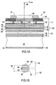
- Figure 1A is a cross-sectional view of a VCSEL according to the invention.
- Figure 1B is an enlarged cross-sectional view of part of the quantum well region of a VCSEL according to the invention.
- Figure 2 is a schematic depiction of a system that can be used for growing the layer structure including a layer of GaNAs in which VCSELs according to the invention are made.
- FIG 1A shows an embodiment 101 of a vertical cavity surface emitting laser (VCSEL) according to the invention.
- the VCSEL 101 generates infra-red light of wavelength ⁇ that is radiated along the optical axis 105.
- the VCSEL is composed of the gallium arsenide (GaAs) substrate 127, the lower mirror region 107 adjacent the substrate, and the upper mirror region 111.
- the upper and lower mirror regions include layers of GaAs or aluminum gallium arsenide (AlGaAs).
- AlGaAs aluminum gallium arsenide
- the active region 125 is sandwiched between the upper and lower mirror regions.
- the active region, the lower minor region and the upper minor region collectively constitute the optical cavity 103, the lateral extent of which in the radial direction r , perpendicular to the optical axis, is defined by the low-conductivity zone 113, which surrounds the core zone 115.
- the active region is composed of the light-generating region 109 sandwiched between the lower cladding layer 137 and the upper cladding layer 139.
- the cladding layers are a doped portion of the gallium arsenide layers 138 and 140.
- the gallium arsenide layers may alternatively be layers of AlGaAs.
- the light-generating region 109 is centered in the active region 125, and is composed of the quantum well region 155 sandwiched between the lower separate confinement heterojunction (SCH) layer 151 and the upper SCH layer 153.
- the lower and upper SCH layers are respectively undoped portions of the lower and upper gallium arsenide layers 138 and 140.
- the quantum well region is composed of at least one quantum well layer 157 of gallium nitride arsenide GaN x As (1- x ) which has a lower bandgap than gallium arsenide.
- the bandgap of gallium nitride arsenide decreases as the fraction of nitrogen x increases.
- the fraction of nitrogen in the gallium nitride arsenide of the quantum well layer is that which gives a bandgap corresponding to light generation at a desired wavelength, greater than one micron.
- a nitrogen fraction of about 0.03 gives a bandgap of 0.95 eV, which corresponds to light generation at 1.3 ⁇ m
- a nitrogen fraction of 0.04 gives a bandgap of 0.8 eV, which corresponds to light generation at 1.55 ⁇ m.
- the thickness of the layers in the upper and lower mirror regions and the thickness of the active layer all correspond to the wavelength of the light generated by the quantum well region.
- Gallium nitride arsenide has a smaller lattice constant than gallium arsenide, since some of the arsenic atoms in gallium arsenide are replaced with nitrogen atoms, which have a substantially smaller covalent bonding distance. Accordingly, there is lattice mismatch between gallium nitride arsenide and pure gallium arsenide. The lattice mismatch increases as the fraction of nitrogen is increased above zero.
- the lattice mismatch is small at nitrogen fractions less than about 10%, so that with layer thicknesses less than about 100 ⁇ , the lattice mismatch can be accommodated by strain in the layers instead of by dislocations.
- the quantum well layer will grow on the lower gallium arsenide layer 138 without dislocations, and the upper gallium arsenide layer 140 and the layers of the upper mirror region 111 will grow on the quantum well layer without dislocations.
- indium gallium nitride arsenide may alternatively be used as the material of the quantum well layer.
- the fractions of indium and nitrogen in the indium gallium nitride arsenide may be set to provide the material of the quantum well layer with a band gap corresponding to light emission at the desired wavelength, greater than one micron, e.g., 1.3 ⁇ m or 1.55 ⁇ m, and a lattice constant equal to that of the GaAs or AlGaAs of the adjacent gallium arsenide layers 138 and 140.
- Figure 1A shows a cross sectional view of the VCSEL 101 in the plane of the optical axis 105 and perpendicular to the plane of the light-generating region 109. It should be noted that Figures 1A and 1B do not show the VCSEL to scale. The thicknesses of all the layers of the VCSEL except the substrate 127 have been increased to show the layers more clearly. In actual devices, the thickness of the substrate is approximately 500 ⁇ m, while the combined thickness of the lower and upper mirror regions 107 and 111 and the active region 125 is about 6-7 ⁇ m.
- the light emission port 129 in the electrode 131 is typically about 10 ⁇ m across.
- the lower mirror region 107 and the upper mirror region 111 each typically include tens of layers, most of the layers have been omitted from the depiction of these regions to simplify the drawing. Also, since the thickness of the light-generating region 109 is small compared with that of the active region 125, the light generating region is shown in more detail in Figure 1B. Finally, the terms upper and lower are respectively used in this description to denote remoteness or proximity of various elements relative to the substrate 127, and not to indicate any particular spatial orientation.
- the VCSEL 101 is one of many VCSELs formed simultaneously by processing operations that epitaxially grow a succession of layers on the surface of a GaAs wafer to form a layer structure. After the layer structure has been formed, the individual VCSELs are defined in the layer structure by implanting to form a low-conductivity zone defining the core zone of each VCSEL. The wafer with the layer structure formed on its surface is then divided into individual VCSELs or arrays of VCSELs.
- the substrate 127 is a small part of a wafer of GaAs typically about 500 ⁇ m thick and about 50-75 mm in diameter.
- the lower mirror region 107 is preferably a distributed Bragg reflector, as shown in Figure 1A.
- Distributed Bragg reflectors have a periodic structure of thin semiconductor or dielectric layers with alternating higher and lower refractive indices.
- the distributed Bragg reflector constituting the lower mirror region 107 may consist of 32.5 pairs of alternating AlAs and GaAs layers, for example, the layers 133 and 135, epitaxially grown on the substrate 127.
- the layers of AlAs and GaAs are preferably grown by molecular beam epitaxy (MBE) or metal-organic chemical vapor deposition (MOCVD).
- Each layer of the distributed Bragg reflector constituting the lower mirror region has a physical thickness of q ⁇ /4 n 1 , where n 1 is the refractive index of the material of the layer, and q is an odd integer.
- Aluminum gallium arsenide (AlGaAs) which has almost the same lattice constant as that of GaAs, may be used in the lower mirror region instead of AlAs or instead of GaAs.
- AlGaAs which has almost the same lattice constant as that of GaAs, may be used in the lower mirror region instead of AlAs or instead of GaAs.
- Two different forms of AlGaAs, each with a different fraction of aluminum may also be used instead of both the AlAs and GaAs.
- AlGaAs may be used between the AlAs and the GaAs in the lower mirror region to increase the electrical conductivity of the lower mirror region.
- the active region 125 is grown on the lower mirror region 107.
- the active region has a total thickness of p ⁇ /2 n 2 where n 2 is the average refractive index of the materials of the active region, and p is an integer.
- the active region is composed of the light-generating region 109 sandwiched between the lower cladding layer 137 and the upper cladding layer 139.
- the lower cladding layer is a layer of doped GaAs epitaxially grown on the lower mirror region, preferably by MBE or MOCVD.
- the light-generating region 109 is undoped, and is grown on the lower cladding layer. The light-generating region will be described in more detail below.
- the upper cladding layer is a layer of GaAs epitaxially grown on the light-generating region, preferably by MBE or MOCVD.
- Aluminum gallium arsenide may be used instead of gallium arsenide in the upper and lower cladding layers.
- the lower and upper cladding layers consitute doped portions of the lower and upper gallium arsenide layers 138 and 140.
- the lower and upper gallium arsenide layers also respectively include the lower and upper SCH layers, part of the light generating region 109.
- the upper minor region 111 is preferably a distributed Bragg reflector, as shown in Figure 1A.
- the distributed Bragg reflector constituting the upper mirror region 111 may consist of 20 pairs of alternating AlAs and GaAs layers epitaxially grown on the active region 125, preferably by MBE or MOCVD.
- Each layer of the distributed Bragg reflector constituting the upper mirror layer has a physical thickness of q ⁇ /4 n 1 , where n 1 is the refractive index of the material of the layer, and q is an odd integer.
- Aluminum gallium arsenide may be used in the upper mirror region similarly to its use, described above, in the lower mirror region.
- the upper mirror region 111 may alternatively be a distributed Bragg reflector composed of alternating dielectric layers, for example, layers of silicon dioxide SiO 2 and titanium dioxide TiO 2 . Silicon nitride Si 3 N 4 may be used instead of silicon dioxide.
- a distributed Bragg reflector composed of alternating dielectric layers has fewer pairs of layers than a distributed Bragg reflector composed of alternating semiconductor layers of equal reflectivity.
- the materials of the lower and upper mirror regions 107 and 111, the materials of the lower and upper cladding layers 137 and 139 of the active region 125, and the material of the substrate 127 are doped with suitable dopants to make them electrically conductive.
- the lower mirror region is doped with either p-type dopant or an n-type dopant, and the upper mirror region is doped with the opposite type of dopant.
- the lower cladding layer is doped to have the same conductivity type (p-type or n-type) as the lower minor layer.
- the upper cladding layer is doped to have the same conductivity type as the upper mirror layer.
- the light generating layer 109 is undoped. Therefore, the mirror regions 107 and 111, their adjacent cladding layers 137 and 139, and the light-generating region 109 collectively form a p-i-n or an n-i-p diode.
- the substrate 127 is doped with an n-type dopant. If the lower mirror region 107 is doped with a p-type dopant, an additional pair of layers (not shown), repectively degeneratively doped with a p-type dopant and an n-type dopant to form a tunnel junction, is interposed between the lower mirror region and the substrate.
- the tunnel junction provides a conduction path with a low voltage drop between the lower mirror region and the substrate.
- the lower mirror region 107, the upper mirror region 111 and the active region 125 form the optical cavity 103 in which the distributed Bragg reflectors constituting the lower and upper mirror regions 107 and 111 reflect most of the light generated in the light-generating region 109 back into the active region 125.
- Wave interference within the layers of the distributed Bragg reflectors reduces the light to standing waves of wavelength ⁇ .
- the low-conductivity zone 113 is formed in the upper mirror region 111 by ion implantation, preferably performed using hydrogen ions. Ions of other suitable elements, such as helium or oxygen, may alternatively be used. Because ion implantation disrupts the crystal structure, the low-reflectivity zone does not usually extend into the active region 125, but stops short in the upper mirror region as shown.
- the low-conductivity zone 113 may alternatively be defined by forming a native oxide region surrounding the core zone 115 in at least one layer of the upper mirror region 111.
- the low-conductivity zone 113 defines the lateral extent of the optical cavity 103 in the plane of the light-generating region 109.
- the lateral extent of the optical cavity corresponds approximately to the boundary 159 between the core zone 115 and the low-conductivity zone.
- the implantation in the low-conductivity zone causes the upper minor region to have a lower electrical conductivity in the low-conductivity zone than in the core zone. This confines the flow of laser current through the upper mirror region to the core zone, and also confines the flow of laser current through the active region 125 to a zone substantially coextensive with the core zone.
- the electrode 131 is a metallized electrode of the appropriate type for the conductivity type of the material of the upper mirror region 111, and is located on the surface 147 of the upper mirror region, remote from the active region 125.
- the electrode is centered on the optical axis 105.
- the electrode is formed to include the light emission port 129 through which the light generated by the VCSEL is emitted.
- the light emission port is also centered on the optical axis, and has a lateral extent less than that of the core zone 115 so that part of the electrode 131 overlaps the core zone to provide a low resistance path for current to flow between the electrode and the core zone.
- the top layer of the upper mirror region may be a current-spreading layer composed of highly-doped GaAs that provides a highly-conductive path between the electrode and the core zone.
- An upper minor region 111 composed of a distributed Bragg reflector having alternating dielectric layers is non-conductive, and requires that the electrode 131 contact the active region 125 directly.
- the electrode 143 is located on the back surface 145 of the substrate 127, and is a metallized electrode of the appropriate type for the conductivity type of the substrate.
- the light-generating region 109 is shown in greater detail in Figure 1B.
- the light-generating region is located centrally in the active region 125.
- the light-generating region is composed of the quantum well region 155 sandwiched between the lower separate confinement heterojunction (SCH) layer 151 and the upper SCH layer 153.
- Figure 1B shows a single quantum well structure in which the quantum well region is composed of the single quantum well layer 157.
- a multiple quantum well structure in which the quantum well region is composed of multiple quantum well layers separated by respective barrier layers, increases the optical gain of the light-generating region.
- at least one additional quantum well layer and a respective barrier layer (not shown) is interposed between the quantum well layer 157 and one of the adjacent SCH layers.
- the lower SCH layer 151 and the upper SCH layer 153 are preferably layers of GaAs or AlGaAs and constitute an undoped portion of the lower gallium arsenide layer 138 and the upper gallium arsenide layer 140, respectively.
- the lower gallium arsenide layer is grown using doped GaAs or AlGaAs to form the lower cladding layer 137, and the lower SCH layer is formed by continuing the growth process with the supply of the dopant turned off.
- the upper gallium arsenide layer is grown on the quantum well region 155, initially using undoped GaAs or AlGaAs to form the upper SCH layer.
- the upper cladding layer 139 is then formed by turning a supply of a suitable dopant on and continuing the growth of the upper gallium arsenide layer.
- the quantum well layer 157 is a layer of gallium nitride arsenide GaN x As 1- x .
- Gallium arsenide has a band gap of 1.42 eV, which corresponds to light emission at a wavelength of less than one micron.
- Gallium nitride arsenide in which the fraction of nitrogen in the range of about 0.01-0.1, i.e., 0.01 ⁇ x ⁇ 0.1, has a band gap that corresponds to light emission at wavelengths of greater than one micron.
- a nitrogen fraction x of about 0.03 results in a band gap of about 0.95 eV, which corresponds to light emission at a wavelength of about 1.3 ⁇ m
- a nitrogen fraction of about 0.04 results in a band gap of about 0.8 eV, which corresponds to light emission at a wavelength of about 1.55 ⁇ m.
- a nitrogen fraction x of greater than zero in gallium nitride arsenide GaN x As 1- x causes a lattice mismatch between the gallium nitride arsenide of the quantum well layer 157 and the GaAs or AlGaAs of the adjacent gallium arsenide layers 138 and 140.
- Nitrogen has a much smaller covalent radius than arsenic, so replacing some of the arsenic atoms in gallium arsenide with nitrogen atoms causes the resulting gallium nitride arsenide to have a smaller lattice constant from that of gallium arsenide.
- Increasing the nitrogen fraction decreases the critical thickness at which lattice defects, such as dislocations, occur in the quantum well layer.
- Lattice defects allow the quantum well layer to relax to its natural, unstrained lattice constant, but disrupt the electrical parameters of the light-generating region 109, and may impair the reliability of the VCSEL.
- a nitrogen fractio n x significantly higher than about 0.1 may result in a critical thickness less than the desired thickness of the quantum well layer.
- the fraction of nitrogen in the gallium nitride arsenide and the thickness of the quantum well layer are set to prevent such dislocations.
- a higher maximum nitrogen fraction can be used if the thickness of the quantum well layer is small. In a practical embodiment, the nitrogen fraction was about 0.03 and the quantum well layer 157 was about 80 ⁇ thick.
- the quantum well layer has to be lattice matched to the adjacent gallium arsenide layers 138 and 140.
- the lower gallium arsenide is lattice matched to the lower mirror region 107 and the substrate 127. This can be done by using gallium indium nitride arsenide Ga 1- y In y N x As 1- x as the material of the quantum well layer.
- Indium has a greater covalent bonding radius than gallium, so substituting some of the gallium atoms in gallium nitride arsenide with indium atoms results in gallium indium nitride arsenide with a greater lattice constant than pure gallium nitride arsenide with the same value of x .
- the increase in the lattice constant depends on the indium fraction y .
- the lattice constant of gallium indium nitride arsenide can be matched that of the gallium arsenide substrate 127, and its band gap can be set to that corresponding to light emission at the desired wavelength, greater than one micron.
- PHYS., 1273-1275 (1996 February) report photoluminescence at about 1230 ⁇ from a 70 ⁇ single quantum well structure with a quantum well layer of Ga 0.7 In 0.3 N 0.01 As 0.99 .
- a nitrogen fraction of about 0.03, corresponding to light generation at about 1.3 ⁇ m, would require a larger value of the indium fraction y in the range of about 0.04 to about 0.14, with a preferred value of 0.09, to maintain lattice matching with the GaAs or AlGaAs of the adjacent gallium arsenide layers 138 and 140.
- Other materials with the potential for lattice matching with GaAs or AlGaAs, and having a band gap sufficiently low for light generation at desired wavelengths greater than one micron include aluminum indium nitride arsenide Al 1- y In y N x As 1- x , and aluminum gallium indium nitride arsenide Al z Ga 1- y - z In y N x As 1- x .
- indium nitride arsenide InN x As 1- x
- indium nitride arsenide has a lattice constant that matches that of the GaAs or AlGaAs of the adjacent gallium arsenide layers 138 and 140.
- Indium nitride arsenide also has a band gap sufficiently low for light generation at wavelengths greater than one micron.
- the lattice constant of gallium arsenide is 5.66 ⁇ , and that of aluminum gallium arsenide is very similar.
- the lattice constant of indium arsenide is 6 ⁇ , whereas that of indium nitride is 5 ⁇ .
- the lattice constant of indium nitride arsenide InN x As 1- x can be made to match that of gallium arsenide or aluminum gallium arsenide by selecting the appropriate value of x .
- the bandgap of indium arsenide is 0.36 eV and that of indium nitride is 2.2 eV.
- values of the fraction x of nitrogen in indium nitride arsenide InN x As 1- x below a first threshold value result in a band gap less than or equal to 0.95 eV, which corresponds to light generation at 1.3 ⁇ m
- values below a second threshold value result in a band gap less than or equal to 0.8 eV, which corresponds to light generation at 1.55 ⁇ m.
- the value of x at which the lattice constant of an indium gallium arsenide quantum well layer 157 matches that of the GaAs or AlGaAs of the adjacent gallium arsenide layers 138 and 140 may not be the value of x that results in a band gap corresponding to light generation at the desired wavelength, greater than one micron, e.g., 1.3 or 1.55 ⁇ m.
- Adding gallium, aluminum or both gallium and aluminum to indium nitride arsenide results in a material that is lattice matched to the GaAs or AlGaAs of the gallium arsenide layers 138 and 140 and has a bandgap corresponding to light generation at a desired wavelength, greater than one micron, e.g., 1.3 or 1.55 ⁇ m, as described above.
- the fraction of gallium and/or aluminum that must be added to produce the desired band gap and lattice constant depends on the thickness of the quantum well layer.
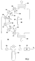
- Figure 2 shows the arrangement of an example of a system that may be used to make long-wavelength infra-red VCSELs having at least one gallium nitride arsenide quantum well layer.
- a similar system can be used to make long-wavelength infra-red VCSELs having at least one gallium indium nitride arsenide, aluminum indium nitride arsenide, or aluminum gallium indium nitride arsenide quantum well layer.
- the system shown is used to make multiple VCSELs simultaneously on a gallium arsenide water by eptaxially growing a layer structure on the water using gas-source molecular beam epitaxy (MBE).
- MBE gas-source molecular beam epitaxy
- the layer structure may alternatively be grown on the water in other ways, such as metal-organic chemical vapor deposition (MOCVD), using a different type of system.
- MOCVD metal-organic chemical vapor deposition
- the water with its layer structure is divided into individual VCSELs by implantation to form a low-conductivity zone that surrounds the core zone of each VCSEL.
- the back side of the wafer is metallized, and an electrode connected to the core zone of each VCSEL is formed on the top surface of the layer structure.
- the wafer with its layer structure is physically divided into individual VCSELs or VCSEL arrays.
- the wafer 201 is mounted on the water holder 202 located inside the growth chamber 203. Included in the water holder, but not shown, are elements for heating the wafer to a predetermined temperature and for measuring the temperature of the wafer.
- the interior of the growth chamber 203 is connected to an ion pump and a cryo pump (not shown) via the outlets 204 and 206, respectively. These pumps maintain a base pressure in the range of about 10 -10 to about 10 -11 torr inside the growth chamber. However, the pressure will rise above the base pressure when fluxes of atoms are introduced into the growth chamber.
- the system includes a series of load locks (not shown) to enable wafers to be introduced into the interior ofthe growth chamber without exposing the interior to atmospheric contamination.
- a number of effusion cells for example, the effusion cells 210, 212, 214, 216 and 218, also communicate with the interior of the growth chamber 203 and face the water 201.
- Effusion cells are also known in the art as Knudsen cells (K-cells) or source furnaces.
- K-cells Knudsen cells
- Each effusion cell is the source of a flux of atoms or molecules of a different chemical element that will be a constituent of the materials of the layers grown on the surface of the water 201.
- each effusion cell includes a heating element for heating the chemical element in the effusion cell to a predetermined temperature, and a temperature sensor for measuring the temperature of the chemical element in the effusion cell.
- the effusion cells 210, 212, 214, 216 and 218 respectively include the remotely-operated shutters 230, 232, 234, 236 and 238 that control the flux of atoms or molecules generated by the effusion cell.
- a respective chemical element is placed in solid form in each effusion cell.
- aluminum is placed in the effusion cell 210
- gallium is placed in the effusion cell 212
- beryllium is placed in the effusion cell 214
- silicon is placed in the effusion cell 216
- arsenic is placed in the effusion cell 218.
- each of the effusion cells 210-218 is heated by the heating element to a predetermined temperature to generate the flux of atoms or molecules directed towards the water 201. Whether the flux is of atoms or molecules depends on the element. To simplify the following description, atoms and molecules will be referred to collectively as "atoms.” The flux of the atoms from each effusion cell depends on the temperature of the effusion cell and the position of the shutter of the effusion cell.
- the system 200 also includes the electron cyclotron resonance (ECR) plasma source 220 that provides the nitrogen constituent of gallium nitride arsenide.
- ECR electron cyclotron resonance
- the lower mirror region 107 is composed of alternating layers of AlAs and GaAs or AlGaAs epitaxially grown on the GaAs substrate 127.
- the first layer of the layer structure grown on the wafer 201 is a layer of AlAs.
- wafer is mounted on the substrate holder 202 in the interior of the growth chamber 203. The wafer is then heated to a temperature between about 500°C and 700°C.
- the effusion cell 210 is heated to a temperature at which it generates the required flux of aluminum atoms. To provide a growth rate of about 1 ⁇ m/hour, a flux of about 6 ⁇ 10 14 aluminum atoms/cm 2 /sec is required.
- the effusion cell 218 is heated to a temperature at which it generates a substantially greater flux of arsenic atoms than the flux of aluminum atoms generated by the effusion cell 210.
- the fluxes of atoms impinge on the surface of the water and atoms from the fluxes bond to the wafer and to one another to form an epitaxial layer of AlAs having the same crystalline structure as that of the GaAs of the wafer. Excess arsenic atoms that have not bonded to corresponding aluminum atoms are removed by the pumps connected to the outlets 204 and 206 or are deposited on the inside walls of the growth chamber 203.
- the effusion cell 214 and the effusion cell 216 are heated to a temperature at which they respectively generate beryllium or silicon atoms at a flux of between about 10 -6 and about 10 -1 of that of the flux of aluminum atoms generated by the effusion cell 210. Then, either the shutter 234 of the effusion cell 214 or the shutter 236 of the effusion cell 216 is opened to provide a flux of dopant to dope the layer of AlAs. If the shutter 234 of the effusion cell 214 is opened, the flux of beryllium atoms dopes the AlAs p-type, whereas if the shutter 236 of the effusion cell 216 is opened, the flux of silicon atoms dopes the AlAs n-type.
- the effusion cell 212 is also heated to a temperature at which it generates a flux of gallium atoms comparable to the flux of aluminum atoms generated by the effusion cell 210.
- the layer of AlAs reaches the required thickness of ⁇ /4 n 3 , where ⁇ is the desired wavelength of the light to be generated by the VCSEL (e.g., 1.3 or 1.55 ⁇ m) and n 3 is the refractive index of AlAs
- the shutter 232 of the effusion cell 212 is opened to admit the flux of gallium atoms into the growth chamber 203, and, at the same time, shutter 230 on the effusion cell 210 is closed to switch off the flux of aluminum atoms entering the growth chamber.
- the flux of atoms from the effusion cells 218 and either 214 or 216 is maintained.
- the gallium and arsenic atoms deposit on the AlAs layer to form GaAs having the same crystalline structure as that of the AlAs layer, and, hence, of the underlying GaAs water.
- n 4 is the refractive index of GaAs
- another layer of AlAs is grown on the layer of GaAs by opening the shutter 230 of the effusion cell 210 and closing the shutter 232 of the effusion cell 212 to replace the flux of gallium atoms with a flux of aluminum atoms.
- the flux of atoms from the effusion cells 218 and either 214 or 216 is maintained.
- the shutters 230 and 232 of the effusion cells 210 and 212, respectively, are cycled as just described about 30 times to form the lower mirror region 107 composed of about 30 pairs of alternating doped AlAs and GaAs layers.
- the shutters 230 and 232 of the effusion cells 210 and 212 may be positioned so that fluxes of both aluminum atoms and gallium atoms are simultaneously directed towards the wafer 201 so that layers of AlGaAs can be grown instead of, or in addition to, the layers of AlAs and GaAs, as described above.
- a layer of GaAs or AlGaAs is then grown in the way just described on the top layer of the lower mirror region to form the lower gallium arsenide layer 138.
- the lower gallium arsenide layer is initially doped with a flux of dopant from the effusion cell 214 or 216 to have the same conductivity type as the lower mirror region and to form the lower cladding layer 137.
- the shutter 234 or 236 of the respective effusion cell 214 or 216 supplying the dopant is closed to such off the flux of dopant.
- the flux from the effusion cells 212 and 218 is maintained to continue growing the gallium arsenide layer by growing additional, undoped, GaAs or AlGaAs on the lower cladding layer to form the lower SCH layer 151.
- gallium nitride arsenide When the lower SCH layer has reached a thickness in the range of about 500-1,000 ⁇ , a layer of gallium nitride arsenide is grown on the lower gallium arsenide layer 138 to form the quantum well layer 157.
- the shutters 232 and 238 of the effusion cells 212 and 218, respectively, are kept open to provide respective streams of gallium atoms and arsenic atoms.
- gallium nitride arsenide cannot simply be made by directing a stream of nitrogen molecules towards the heated wafer 201, together with the fluxes of gallium atoms and arsenic atoms. Molecular nitrogen is too stable for its constituent atoms to bond to the gallium atoms when the nitrogen molecules contact the heated wafer.
- a wafer temperature of over 3,500°C would be required to break the nitrogen molecule into its constituent atoms.
- the system 200 therefore lacks a simple injector for nitrogen gas molecules.
- the electron cyclotron resonance (ECR) plasma source 220 is used to generate a stream of ionized nitrogen molecules and excited nitrogen molecules for injection into the growth chamber 203. Ionized nitrogen molecules and excited nitrogen molecules readily bond with gallium atoms on contact with the heated wafer.
- Nitrogen gas from a suitable source is passed via the mass flow controller (MFC) 222, the valve 224, the gas purification filter 226, and the valve 228 to the ECR plasma source 220.
- the ECR plasma source subjects the electrons of the nitrogen gas molecules to microwave energy at a frequency of about 2.45 GHz, which is their cyclotron resonance frequency. This ionizes some of the nitrogen molecules and excites others of the nitrogen molecules to a higher-energy state.
- the resulting stream of such molecules passes from the ECR plasma source 220 into the growth chamber 203 and meets the streams of gallium atoms and arsenic atoms at the surface of the heated wafer 201.
- the constituent atoms of such nitrogen molecules bond with the gallium atoms on contact with the heated wafer.
- the flow of nitrogen into the ECR plasma source is set such that nitrogen atoms constitute a fraction of between 0.01 and 0.1 of the combined arsenic and nitrogen atoms.
- the flow is set such that nitrogen atoms constitute a fraction of about 0.03 of the combined arsenic and nitrogen atoms when the VCSEL 101 is to generate light at 1.3 ⁇ m, and about 0.04 of the combined arsenic and nitrogen atoms when the VCSEL 101 is to generate light at 1.55 ⁇ m.
- the optical gain of the VCSEL 101 is highly dependent on the optical quality of the layer structure of the VCSEL, and, in particular, on the optical quality of the quantum well region 155.
- the optical quality of the quantum well region depends in turn on the quality of the crystal structure of the material of the quantum well layer 157.
- the optical quality of the layers grown on the quantum well layer depends on the quality of the crystal structure of the quantum well layer.
- the quantum well layer must be grown in a way that provides a high-quality crystal structure.
- the ECR plasma source 220 can generate nitrogen ions and excited nitrogen atoms with sufficient energy to disrupt the crystal structure of the gallium nitride arsenide of the quantum well layer.
- the ECR plasma source may incorporate a graphite electrode to moderate the energy of the nitrogen ions and improve the optical quality of the quantum well layer.
- lower-energy nitrogen ions and excited nitrogen atoms may be generated using an RF plasma source.
- a stream of a chemical source of nitrogen such as ammonia or hydrogen azide may be directed towards the surface of the wafer 201. If ammonia is used as the nitrogen source, it can be pre-cracked prior to injection into the growth chamber 203, or it can be cracked by the temperature of the wafer.
- the above-described layer structure may be epitaxially grown on the wafer 201 using MOCVD instead of gas source MBE.
- MOCVD MOCVD
- hydrazine, dimethyl hydrazine, or ammonia may be used as nitrogen precursors in forming the quantum well layer 157.
- the temperature of the wafer 201 may be changed from that at which the lower mirror region 107 and the lower gallium arsenide layer 138 were grown.
- the quality of the crystal structure of the quantum well layer is optimized by growing the quantum well layer with the wafer at as high a temperature as possible. This temperature may be as high as about 800°C when the quantum well layer is a layer of gallium nitride arsenide grown by gas-source MBE. Temperatures as high as about 1100°C may be used when a gallium nitride arsenide quantum well layer is grown using MOCVD. These maximum temperatures must be reduced when the quantum well layer includes indium. For example, de-sorption of indium may occur at temperatures above about 600°C when a layer of gallium indium nitride arsenide is grown by gas-source MBE.
- the gallium nitride arsenide layer is continued until the quantum well layer 157 reaches the required thickness in the range of 50-100 ⁇ .
- the flow of nitrogen gas to the ECR plasma source 220 is then turned off.
- the flow of nitrogen gas may be maintained and the supply of microwave energy to the ECR plasma source turned off.
- the resulting non-ionized/non-excited nitrogen molecules do not combine with the gallium atoms on contact with the heated wafer 201, and are removed from the growth chamber 203 by the pumps connected to the outlets 204 and 206.
- the shutters 232 and 238 of the effusion cells 212 and 218, respectively are kept open to grow a layer of GaAs on the gallium nitride arsenide of the quantum well layer. Also, the shutter 230 of the effusion cell 210 may be re-opened to grow a layer of AlGaAs instead of a layer of GaAs.
- the gallium nitride arsenide of the quantum well layer is strained, and has the same lattice constant as the underlying lower gallium arsenide layer 138, the layer of GaAs or AlGaAs grows epitaxially on top of the quantum well layer with the same crystal structure as that of the lower gallium arsenide layer.
- the layer of GaAs or AlGaAs on the quantum well layer 157 is stopped with the layer reaches a thickness of about 300 ⁇ .
- This layer (not shown) then constitutes a barrier layer between the quantum well layer and an adjacent additional quantum well layer (not shown).
- the additional quantum well layer is grown on the barrier layer by switching on the supply of nitrogen gas or the supply of microwave energy to the ECR plasma source 220 and continuing growth until the additional quantum well layer reaches a thickness in the range of about 50-100 ⁇ .
- Several layer pairs, each composed of a GaAs or AlGaAs barrier layer and a gallium nitride arsenide additional quantum well layer, may be grown on the quantum well layer 157 as just described.
- a layer of GaAs or AlGaAs is grown on the uppermost quantum well layer (or the quantum well layer 157 in a single quantum well structure) to form the upper gallium arsenide layer.
- the GaAs or AlGaAs initially deposited is undoped, and constitutes the upper SCH layer 153.
- shutter 234 of the effusion cell 214 or the shutter 236 of the effusion cell 216 is opened, and the shutters 232 and 238 of the effusion cells 212 and 218, respectively, are kept open to continue growth of the upper gallium arsenide layer 140 to form the upper cladding layer 139.
- the shutter 230 of the effusion cell 210 may also be opened or kept open to provide an additional stream of aluminum atoms. Beryllium atoms from the effusion cell 214 or silicon atoms from the effusion cell 216 dope the upper cladding layer for the opposite conductivity type to that of the lower cladding layer 139 and lower mirror region 107.
- the shutter 234 of the effusion cell 214 was open when the lower mirror region and lower cladding layer were grown, the shutter 236 of the effusion cell 216 is opened when the upper cladding layer is grown.
- the shutter 236 of the effusion cell 216 was open when the lower mirror region and lower cladding layer were grown, the shutter 234 of the effusion cell 214 is opened when the upper cladding layer is grown.
- a layer of AlAs constituting the first layer of the upper mirror region 111 is grown on the upper gallium arsenide layer 140.
- the AlAs layer is grown by opening the shutter 230 of the effusion cell 210 and closing the shutter 232 of the effusion cell 212 to switch off the flux of gallium atoms.
- the shutters of the effusion cells 218 and either 214 or 216 are kept open.
- the shutters 230 and 232 of the effusion cells 210 and 212, respectively, are cycled about 20 times to form the upper mirror region 111.
- the upper mirror region is composed of about 20 pairs of alternating AlAs and GaAs or AlGaAs layers.
- the shutter 234 or 236 of the effusion cell 214 or 216 may be further opened during growth of the final one or two layers to increase the doping level so that this layer or these layers act as a current spreading layer. Growing the final layer of the upper mirror region completes formation of the layer structure on the wafer 201.
- the shutters 230 and 232 of the effusion cells 210 and 212 may be positioned so that fluxes of both aluminum atoms and gallium atoms are simultaneously directed towards the wafer 201 so that layers of AlGaAs can be grown instead of, or in addition to, the layers of AlAs and GaAs, as described above.
- the top surface 147 of the upper mirror region 111 of the layer structure is then masked to define the core zone of each VCSEL on the wafer. Ions, such as hydrogen ions, are then implanted through the top surface to form the low conductivity zone that surrounds the core zone of each VCSEL.
- the mask defines the core zone 115 of the VCSEL 101, and ions are implanted to form the low conductivity zone 113 surrounding the core zone of the VCSEL 101.
- the top surface 147 of the upper mirror region 111 of the layer structure and bottom surface 145 of the wafer are then metallized with a metal such as gold or aluminum.
- the layer of metal deposited on the top surface of the upper mirror region is then masked to define the annular electrode of each VCSEL on the water.
- the mask defines the annular electrode 131 of the VCSEL 101.
- the layer of metal is then etched to form the electrodes. Finally, the water is divided into individual VCSELs, including the VCSEL 101, or into arrays of VCSELs.
Abstract
A vertical cavity surface emitting laser (VCSEL) (101) that generates light having a desired
wavelength, greater than one micron. The laser comprises a substrate (127), a lower mirror
region (107), an active region (125) and an upper mirror region (111). The substrate consists
essentially of GaAs. The lower mirror region is adjacent the substrate and is lattice matched to the
substrate. The active region is sandwiched between the upper and lower mirror regions, and
includes a central quantum well region (155) and a gallium arsenide layer (138, 140) sandwiched
between the quantum well region and each of the lower mirror region and the upper mirror region.
The central quantum well region includes a quantum well layer (157) consisting essentially of
GaN x As(1-x). The GaN x As(1-x) of the quantum well layer has a lattice constant and a band gap
dependent on x. The value of x sets the bandgap of the GaN x As(1-x) of the quantum well layer to a
value corresponding to light generation at the desired wavelength, greater than one micron. Each
gallium arsenide layer (138, 140) is a layer of a material consisting essentially of GaAs or AlGaAs,
and is lattice matched to the substrate. The quantum well layer may additionally include a fraction
of indium to lattice match the quantum well layer to the substrate.
Description
The invention relates to light-generating semiconductor devices, and, in particular, to a vertical
cavity surface-emitting laser that generates infra-red light at wavelengths greater than one micron and
is constructed on a gallium arsenide substrate.
Semiconductor light-emitting devices, such as vertical cavity surface-emitting lasers (VCSELs),
are manufactured using several substrate materials. These materials include gallium arsenide
(GaAs), gallium phosphide (GaP), and indium phosphide (InP). A light-emitting device is made by
epitaxially growing various materials having different bandgaps on the substrate. By selecting the
appropriate materials, a light-emitting device is formed that generates light at the required wavelength.
However, to obtain high quality light-emitting devices, the materials grown on the substrate must be
closely lattice matched to the substrate. If materials grown on the substrate are pseudomorphic, i.e.,
not lattice matched to the substrate, the thickness of the layers of the grown materials must be limited
to prevent dislocations from occurring in the grown materials.
Gallium arsenide is the most common, lowest cost, and most practical substrate material for use
in making light-emitting devices. However, due to the requirements that layers of materials grown on
the substrate be lattice matched to the substrate to prevent dislocations in the grown layers, the
wavelengths obtainable from light-emitting devices made by growing materials in the aluminum,
indium, gallium, arsenide, phosphide (AlInGaAsP) material system on a GaAs substrate are limited
to the range from 0.6 µm to 1.0 µm.
The glasses used as the core material for the optical fibres used in long-haul optical fiber
communication systems have their maximum transmissivity at infra-red wavelengths substantially
longer than one micron, i.e., substantially longer than the wavelengths that can be generated by
devices made by growing layers of materials in the (AlInGaAsP) material system on a GaAs substrate.
The most common wavelengths used in long-haul optical fiber communication systems are 1.3 µm
and 1.55 µm. Light-emitting devices generating light at these wavelengths have up to now been grown
on InP substrates.
Indium phosphide has several disadvantages as a substrate material. First, InP substrates are
considerably more expensive than GaAs substrates of the same size. Second, InP substrates are not
available in such large diameters as GaAs substrates. This results in a greater per-device fabrication
cost. Third, InP substrates are more brittle than GaAs substrates, and so have greater production
costs due to wafer handling losses than GaAs substrates. Fourth, VCSELS made on InP substrates
have inferior performance to VCSELS made on GaAs substrates, primarily because distributed Bragg
reflectors made in materials lattice matched to InP have a significantly lower reflectivity and electrical
conductivity than distributed Bragg reflectors made in materials lattice matched to GaAs. Aluminum
arsenide (AlAs) is lattice matched to GaAs, and the large refractive index difference between AlAs and
GaAs enables high-reflectivity distributed Bragg reflectors to be made using relatively few pairs of
alternating λ/4n-thick AlAs and GaAs layers. In this, A is the wavelength, in vacuo, of the light
generated by the VCSEL, e.g., 1.3 µm or 1.55 µm, and n is the refractive index of the layer.
Distributed Bragg reflectors made of alternating AlAs and GaAs layers are both electrically and
thermally conductive, and enable high-performance 0.78 µm to 0.98 µm VCSELS to be made.
However, the much smaller refractive index difference between InP and materials lattice-matched to
InP means that a distributed Bragg reflector made using InP requires about 40-60 pairs of layers to
provide the same reflectivity as an AlAs/GaAs reflector with 20-30 pairs of layers. The electrical and
thermal conductivity of distributed Bragg reflectors with such a large number of layers is so low that
adequate device efficiency cannot be attained, and the light output of the device is limited by thermal
considerations.
Accordingly, it is desirable to be able to make light-emitting devices that generate light at
wavelengths longer than 1.0 µm by growing layers of materials on GaAs substrates.
The invention provides a vertical cavity surface emitting laser (VCSEL) that generates light having
a desired wavelength, greater than one micron. The laser comprises a substrate, a lower mirror
region, an active region and an upper mirror region. The substrate consists essentially of GaAs. The
lower minor region is adjacent the substrate and is lattice matched to the substrate. The active region
is sandwiched between the upper and lower mirror regions, and includes a central quantum well
region and a gallium arsenide layer sandwiched between the quantum well region and each of the
lower minor region and the upper minor region. The central quantum well region includes a quantum
well layer consisting essentially of GaN x As(1-x). The GaN x As(1-x) of the quantum well layer has a lattice
constant and a band gap dependent on x. The value of x sets the bandgap of the GaN x As(1-x) of the
quantum well layer to a value corresponding to light generation at the desired wavelength, greater
than one micron. Each gallium arsenide layer is a layer of a material consisting essentially of GaAs
or AlGaAs, and is lattice matched to the substrate.
The VCSEL according to the invention generates infra-red light at a wavelength greater than one
micron, yet is formed on a substrate of GaAs. High quality GaAs substrates are readily available, and
are more rugged and far less expensive than InP substrates. The VCSEL includes a lower mirror
region of materials that are lattice matched to the GaAs substrate. Such a lower mirror region can be
made using GaAs and AlAs. The large refractive index difference between these materials enables
the lower mirror region to have a high electrical and thermal conductivity because relatively few pairs
of layers are required. The VCSEL generates light at a wavelength of greater than one micron using
a quantum well layer of gallium nitride arsenide GaN x As(1-x), where x is less than 0.1. The band gap
of this material is sufficiently low for light generation at such wavelengths, and its lattice constant is
sufficiently close to that of GaAs that a strained thin layer will adopt the lattice constant of GaAs without
dislocations of the crystal structure occurring.
The VCSEL according to the invention generates light in a preferred wavelength range between
about 1.1 µm and 1.6 µm, and the value of x is preferably between 0.01 and 0.1. With values of x of
about 0.03 and 0.04, the VCSEL generates light at wavelengths of 1.3 µm and 1.55 µm, respectively.
These wavelengths are the most common wavelengths used in long-haul optical fiber communication
systems.
The GaN x As(1-x) of the quantum well layer has a critical thickness that depends on the value of
x. The critical thickness of a strained layer is the thickness of the layer at which dislocations of the
crystal structure begin to occur. The quantum well layer has a thickness of less than the critical
thickness.
The quantum well layer may be lattice matched to the gallium arsenide layer by the quantum well
layer being a layer of a material consisting essentially of gallium indium nitride arsenide
Ga(1-y)In y N x As(1-x). The lattice constant and band gap of the Ga(1-y)In y N x As(1-x) of the quantum well layer
depend on x and y. The values of x and y set the lattice constant of the Ga(1-y)In y N x As(1-x) of the
quantum well layer to match the lattice constant of the material of the gallium arsenide layers, and set
the bandgap of the Ga(1-y)In y N x As(1-x) of the quantum well layer to a value corresponding to light
generation at the desired wavelength, greater than one micron.
The value of y may be as high as unity, in which case the quantum well layer is a layer of a
material consisting essentially of indium nitride arsenide Ga(0)In1N x As(1-x). The value of x sets the lattice
constant of the Ga(1-y)In y N x As(1-x) of the quantum well layer to match the lattice constant of the material
of the gallium arsenide layers.
The quantum well layer may alternatively be lattice matched to the gallium arsenide layer by the
quantum well layer being a layer of a material consisting essentially of aluminum gallium indium nitride
arsenide Al z Ga(1-y-z)In y N x As(1-x). The lattice constant and band gap the Al z Ga(1-y-z)In y N x As(1-x) of the
quantum well layer depend on x, y and Z. The values of x, y and z set the lattice constant of the
Al z Ga(1-y-z)In y N x As(1-x) of the quantum well layer to match the lattice constant of the material of the
gallium arsenide layers, and set the bandgap of the Al z Ga(1-y-z)In y N x As(1-x) of the quantum well layer
to a value corresponding to light generation at the desired wavelength, greater than one micron.
The sum of y and z in the Al z Ga(1-y-z)In y N x As(1-x) may be unity, in which case, the quantum well
layer is a layer of aluminum indium nitride arsenide Al z Ga(0)In y N x As(1-x). The values of y and z set the
lattice constant of the Al z Ga(1-y-z)In y N x As(1-x) of the quantum well layer to match the lattice constant of
the material of the gallium arsenide layers, and set the bandgap of the Al z Ga(1-y-z)In y N x As(1-x) of the
quantum well layer to a value corresponding to light generation at the desired wavelength, greater
than one micron.
Figure 1A is a cross-sectional view of a VCSEL according to the invention.
Figure 1B is an enlarged cross-sectional view of part of the quantum well region of a VCSEL
according to the invention.
Figure 2 is a schematic depiction of a system that can be used for growing the layer structure
including a layer of GaNAs in which VCSELs according to the invention are made.
Figure 1A shows an embodiment 101 of a vertical cavity surface emitting laser (VCSEL)
according to the invention. The VCSEL 101 generates infra-red light of wavelength λ that is radiated
along the optical axis 105. The VCSEL is composed of the gallium arsenide (GaAs) substrate 127,
the lower mirror region 107 adjacent the substrate, and the upper mirror region 111. The upper and
lower mirror regions include layers of GaAs or aluminum gallium arsenide (AlGaAs). The active
region 125 is sandwiched between the upper and lower mirror regions. The active region, the lower
minor region and the upper minor region collectively constitute the optical cavity 103, the lateral extent
of which in the radial direction r, perpendicular to the optical axis, is defined by the low-conductivity
zone 113, which surrounds the core zone 115. The active region is composed of the light-generating
region 109 sandwiched between the lower cladding layer 137 and the upper cladding layer 139. The
cladding layers are a doped portion of the gallium arsenide layers 138 and 140. The gallium arsenide
layers may alternatively be layers of AlGaAs.
The light-generating region 109 is centered in the active region 125, and is composed of the
quantum well region 155 sandwiched between the lower separate confinement heterojunction (SCH)
layer 151 and the upper SCH layer 153. The lower and upper SCH layers are respectively undoped
portions of the lower and upper gallium arsenide layers 138 and 140. The quantum well region is
composed of at least one quantum well layer 157 of gallium nitride arsenide GaN x As(1-x) which has a
lower bandgap than gallium arsenide. The bandgap of gallium nitride arsenide decreases as the
fraction of nitrogen x increases. In the VCSEL 101, the fraction of nitrogen in the gallium nitride
arsenide of the quantum well layer is that which gives a bandgap corresponding to light generation at
a desired wavelength, greater than one micron. For example, a nitrogen fraction of about 0.03 gives
a bandgap of 0.95 eV, which corresponds to light generation at 1.3 µm, a nitrogen fraction of 0.04
gives a bandgap of 0.8 eV, which corresponds to light generation at 1.55 µm. In the VCSEL 101, the
thickness of the layers in the upper and lower mirror regions and the thickness of the active layer all
correspond to the wavelength of the light generated by the quantum well region.
Gallium nitride arsenide has a smaller lattice constant than gallium arsenide, since some of the
arsenic atoms in gallium arsenide are replaced with nitrogen atoms, which have a substantially smaller
covalent bonding distance. Accordingly, there is lattice mismatch between gallium nitride arsenide and
pure gallium arsenide. The lattice mismatch increases as the fraction of nitrogen is increased above
zero. For example, in the VCSEL 101, there is a lattice mismatch between the gallium nitride arsenide
of the quantum well layer 155 and the GaAs or AlGaAs of the gallium arsenide layers 138 and 140
and the mirror regions 107 and 111, and the GaAs of the substrate 127. However, the lattice
mismatch is small at nitrogen fractions less than about 10%, so that with layer thicknesses less than
about 100 Å, the lattice mismatch can be accommodated by strain in the layers instead of by
dislocations. Despite the lattice mismatch, the quantum well layer will grow on the lower gallium
arsenide layer 138 without dislocations, and the upper gallium arsenide layer 140 and the layers of
the upper mirror region 111 will grow on the quantum well layer without dislocations.
If strain in the quantum well layer 155 is undesirable, indium gallium nitride arsenide may
alternatively be used as the material of the quantum well layer. The fractions of indium and nitrogen
in the indium gallium nitride arsenide may be set to provide the material of the quantum well layer with
a band gap corresponding to light emission at the desired wavelength, greater than one micron, e.g.,
1.3 µm or 1.55 µm, and a lattice constant equal to that of the GaAs or AlGaAs of the adjacent gallium
arsenide layers 138 and 140.
Figure 1A shows a cross sectional view of the VCSEL 101 in the plane of the optical axis 105 and
perpendicular to the plane of the light-generating region 109. It should be noted that Figures 1A and
1B do not show the VCSEL to scale. The thicknesses of all the layers of the VCSEL except the
substrate 127 have been increased to show the layers more clearly. In actual devices, the thickness
of the substrate is approximately 500 µm, while the combined thickness of the lower and upper mirror
regions 107 and 111 and the active region 125 is about 6-7 µm. The light emission port 129 in the
electrode 131 is typically about 10 µm across. Moreover, since the lower mirror region 107 and the
upper mirror region 111 each typically include tens of layers, most of the layers have been omitted
from the depiction of these regions to simplify the drawing. Also, since the thickness of the light-generating
region 109 is small compared with that of the active region 125, the light generating region
is shown in more detail in Figure 1B. Finally, the terms upper and lower are respectively used in this
description to denote remoteness or proximity of various elements relative to the substrate 127, and
not to indicate any particular spatial orientation.
The VCSEL 101 is one of many VCSELs formed simultaneously by processing operations that
epitaxially grow a succession of layers on the surface of a GaAs wafer to form a layer structure. After
the layer structure has been formed, the individual VCSELs are defined in the layer structure by
implanting to form a low-conductivity zone defining the core zone of each VCSEL. The wafer with the
layer structure formed on its surface is then divided into individual VCSELs or arrays of VCSELs.
The substrate 127 is a small part of a wafer of GaAs typically about 500 µm thick and about 50-75
mm in diameter. The lower mirror region 107 is preferably a distributed Bragg reflector, as shown
in Figure 1A. Distributed Bragg reflectors have a periodic structure of thin semiconductor or dielectric
layers with alternating higher and lower refractive indices. For example, the distributed Bragg reflector
constituting the lower mirror region 107 may consist of 32.5 pairs of alternating AlAs and GaAs layers,
for example, the layers 133 and 135, epitaxially grown on the substrate 127. The layers of AlAs and
GaAs are preferably grown by molecular beam epitaxy (MBE) or metal-organic chemical vapor
deposition (MOCVD). Each layer of the distributed Bragg reflector constituting the lower mirror region
has a physical thickness of qλ/4n 1, where n 1 is the refractive index of the material of the layer, and q
is an odd integer. Aluminum gallium arsenide (AlGaAs), which has almost the same lattice constant
as that of GaAs, may be used in the lower mirror region instead of AlAs or instead of GaAs. Two
different forms of AlGaAs, each with a different fraction of aluminum, may also be used instead of both
the AlAs and GaAs. Finally, AlGaAs may be used between the AlAs and the GaAs in the lower mirror
region to increase the electrical conductivity of the lower mirror region.
The active region 125 is grown on the lower mirror region 107. The active region has a total
thickness of pλ/2n 2 where n 2 is the average refractive index of the materials of the active region, and
p is an integer. The active region is composed of the light-generating region 109 sandwiched between
the lower cladding layer 137 and the upper cladding layer 139. The lower cladding layer is a layer of
doped GaAs epitaxially grown on the lower mirror region, preferably by MBE or MOCVD. The light-generating
region 109 is undoped, and is grown on the lower cladding layer. The light-generating
region will be described in more detail below. The upper cladding layer is a layer of GaAs epitaxially
grown on the light-generating region, preferably by MBE or MOCVD. Aluminum gallium arsenide may
be used instead of gallium arsenide in the upper and lower cladding layers. As noted above, the lower
and upper cladding layers consitute doped portions of the lower and upper gallium arsenide layers 138
and 140. The lower and upper gallium arsenide layers also respectively include the lower and upper
SCH layers, part of the light generating region 109.
The upper minor region 111 is preferably a distributed Bragg reflector, as shown in Figure 1A.
For example, the distributed Bragg reflector constituting the upper mirror region 111 may consist of
20 pairs of alternating AlAs and GaAs layers epitaxially grown on the active region 125, preferably by
MBE or MOCVD. Each layer of the distributed Bragg reflector constituting the upper mirror layer has
a physical thickness of qλ/4n 1, where n 1 is the refractive index of the material of the layer, and q is an
odd integer. Aluminum gallium arsenide may be used in the upper mirror region similarly to its use,
described above, in the lower mirror region.
The upper mirror region 111 may alternatively be a distributed Bragg reflector composed of
alternating dielectric layers, for example, layers of silicon dioxide SiO2 and titanium dioxide TiO2.
Silicon nitride Si3N4 may be used instead of silicon dioxide. A distributed Bragg reflector composed
of alternating dielectric layers has fewer pairs of layers than a distributed Bragg reflector composed
of alternating semiconductor layers of equal reflectivity.
The materials of the lower and upper mirror regions 107 and 111, the materials of the lower and
upper cladding layers 137 and 139 of the active region 125, and the material of the substrate 127 are
doped with suitable dopants to make them electrically conductive. The lower mirror region is doped
with either p-type dopant or an n-type dopant, and the upper mirror region is doped with the opposite
type of dopant. The lower cladding layer is doped to have the same conductivity type (p-type or n-type)
as the lower minor layer. The upper cladding layer is doped to have the same conductivity type
as the upper mirror layer. The light generating layer 109 is undoped. Therefore, the mirror regions
107 and 111, their adjacent cladding layers 137 and 139, and the light-generating region 109
collectively form a p-i-n or an n-i-p diode.
The substrate 127 is doped with an n-type dopant. If the lower mirror region 107 is doped with
a p-type dopant, an additional pair of layers (not shown), repectively degeneratively doped with a p-type
dopant and an n-type dopant to form a tunnel junction, is interposed between the lower mirror
region and the substrate. The tunnel junction provides a conduction path with a low voltage drop
between the lower mirror region and the substrate.
The lower mirror region 107, the upper mirror region 111 and the active region 125 form the
optical cavity 103 in which the distributed Bragg reflectors constituting the lower and upper mirror
regions 107 and 111 reflect most of the light generated in the light-generating region 109 back into
the active region 125. Wave interference within the layers of the distributed Bragg reflectors reduces
the light to standing waves of wavelength λ. By making the distributed Bragg reflector constituting the
upper mirror region 111 less than totally reflective, coherent light having a wavelength of λ is emitted
along the optical axis 105 perpendicular to the plane of the light-generating region 109.
The low-conductivity zone 113 is formed in the upper mirror region 111 by ion implantation,
preferably performed using hydrogen ions. Ions of other suitable elements, such as helium or oxygen,
may alternatively be used. Because ion implantation disrupts the crystal structure, the low-reflectivity
zone does not usually extend into the active region 125, but stops short in the upper mirror region as
shown.
The low-conductivity zone 113 may alternatively be defined by forming a native oxide region
surrounding the core zone 115 in at least one layer of the upper mirror region 111.
The low-conductivity zone 113 defines the lateral extent of the optical cavity 103 in the plane of
the light-generating region 109. The lateral extent of the optical cavity corresponds approximately to
the boundary 159 between the core zone 115 and the low-conductivity zone. The implantation in the
low-conductivity zone causes the upper minor region to have a lower electrical conductivity in the low-conductivity
zone than in the core zone. This confines the flow of laser current through the upper
mirror region to the core zone, and also confines the flow of laser current through the active region
125 to a zone substantially coextensive with the core zone.
The electrode 131 is a metallized electrode of the appropriate type for the conductivity type of the
material of the upper mirror region 111, and is located on the surface 147 of the upper mirror region,
remote from the active region 125. The electrode is centered on the optical axis 105. The electrode
is formed to include the light emission port 129 through which the light generated by the VCSEL is
emitted. The light emission port is also centered on the optical axis, and has a lateral extent less than
that of the core zone 115 so that part of the electrode 131 overlaps the core zone to provide a low
resistance path for current to flow between the electrode and the core zone. The top layer of the
upper mirror region may be a current-spreading layer composed of highly-doped GaAs that provides
a highly-conductive path between the electrode and the core zone.
An upper minor region 111 composed of a distributed Bragg reflector having alternating dielectric
layers is non-conductive, and requires that the electrode 131 contact the active region 125 directly.
The electrode 143 is located on the back surface 145 of the substrate 127, and is a metallized
electrode of the appropriate type for the conductivity type of the substrate.
The light-generating region 109 is shown in greater detail in Figure 1B. The light-generating
region is located centrally in the active region 125. The light-generating region is composed of the
quantum well region 155 sandwiched between the lower separate confinement heterojunction (SCH)
layer 151 and the upper SCH layer 153. To simplify the drawing, Figure 1B shows a single quantum
well structure in which the quantum well region is composed of the single quantum well layer 157.
However, a multiple quantum well structure, in which the quantum well region is composed of multiple
quantum well layers separated by respective barrier layers, increases the optical gain of the light-generating
region. In a multiple quantum well structure, at least one additional quantum well layer and
a respective barrier layer (not shown) is interposed between the quantum well layer 157 and one of
the adjacent SCH layers.
The lower SCH layer 151 and the upper SCH layer 153 are preferably layers of GaAs or AlGaAs
and constitute an undoped portion of the lower gallium arsenide layer 138 and the upper gallium
arsenide layer 140, respectively. The lower gallium arsenide layer is grown using doped GaAs or
AlGaAs to form the lower cladding layer 137, and the lower SCH layer is formed by continuing the
growth process with the supply of the dopant turned off. The upper gallium arsenide layer is grown
on the quantum well region 155, initially using undoped GaAs or AlGaAs to form the upper SCH layer.
The upper cladding layer 139 is then formed by turning a supply of a suitable dopant on and
continuing the growth of the upper gallium arsenide layer.
The quantum well layer 157 is a layer of gallium nitride arsenide GaN x As1-x . Gallium arsenide
has a band gap of 1.42 eV, which corresponds to light emission at a wavelength of less than one
micron. Gallium nitride arsenide in which the fraction of nitrogen in the range of about 0.01-0.1, i.e.,
0.01 ≤ x ≤ 0.1, has a band gap that corresponds to light emission at wavelengths of greater than one
micron. For example, a nitrogen fraction x of about 0.03 results in a band gap of about 0.95 eV, which
corresponds to light emission at a wavelength of about 1.3 µm, and a nitrogen fraction of about 0.04
results in a band gap of about 0.8 eV, which corresponds to light emission at a wavelength of about
1.55 µm.
A nitrogen fraction x of greater than zero in gallium nitride arsenide GaN x As1-x causes a lattice
mismatch between the gallium nitride arsenide of the quantum well layer 157 and the GaAs or AlGaAs
of the adjacent gallium arsenide layers 138 and 140. Nitrogen has a much smaller covalent radius
than arsenic, so replacing some of the arsenic atoms in gallium arsenide with nitrogen atoms causes
the resulting gallium nitride arsenide to have a smaller lattice constant from that of gallium arsenide.
However, with a value of x of about 0.03, which is sufficient to provide gallium nitride arsenide with a
bandgap low enough for light emission at a wavelength of 1.3 µm, and a quantum well layer thickness
of less than about 100 Å, the resulting lattice mismatch can simply be accommodated by strain in the
layers.
Increasing the nitrogen fraction decreases the critical thickness at which lattice defects, such as
dislocations, occur in the quantum well layer. Lattice defects allow the quantum well layer to relax to
its natural, unstrained lattice constant, but disrupt the electrical parameters of the light-generating
region 109, and may impair the reliability of the VCSEL. For example, a nitrogen fraction x significantly
higher than about 0.1 may result in a critical thickness less than the desired thickness of the quantum
well layer. Accordingly, the fraction of nitrogen in the gallium nitride arsenide and the thickness of the
quantum well layer are set to prevent such dislocations. A higher maximum nitrogen fraction can be
used if the thickness of the quantum well layer is small. In a practical embodiment, the nitrogen
fraction was about 0.03 and the quantum well layer 157 was about 80 Å thick.
If strain in the quantum well layer 157 is undesirable, or if the nitrogen fraction required to
produce the band gap corresponding to the desired wavelength results in a critical thickness less than
the desired thickness of the quantum well layer, the quantum well layer has to be lattice matched to
the adjacent gallium arsenide layers 138 and 140. The lower gallium arsenide is lattice matched to
the lower mirror region 107 and the substrate 127. This can be done by using gallium indium nitride
arsenide Ga1-y In y N x As1-x as the material of the quantum well layer. Indium has a greater covalent
bonding radius than gallium, so substituting some of the gallium atoms in gallium nitride arsenide with
indium atoms results in gallium indium nitride arsenide with a greater lattice constant than pure gallium
nitride arsenide with the same value of x. The increase in the lattice constant depends on the indium
fraction y. With an appropriate choice of the values of the nitrogen fraction x and the indium fraction
y, the lattice constant of gallium indium nitride arsenide can be matched that of the gallium arsenide
substrate 127, and its band gap can be set to that corresponding to light emission at the desired
wavelength, greater than one micron. For example, M. Kondow et a., GalnNAs: a Novel Material for
Long-Wavelength Range Laser Diodes with Excellent High-Temperature Performance, 35 JP. J. APPL.
PHYS., 1273-1275 (1996 February) report photoluminescence at about 1230 Å from a 70 Å single
quantum well structure with a quantum well layer of Ga0.7In0.3N0.01As0.99. A nitrogen fraction of about
0.03, corresponding to light generation at about 1.3 µm, would require a larger value of the indium
fraction y in the range of about 0.04 to about 0.14, with a preferred value of 0.09, to maintain lattice
matching with the GaAs or AlGaAs of the adjacent gallium arsenide layers 138 and 140. A nitrogen
fraction of about 0.04, corresponding to light generation at about 1.55 µm, would require a value of
the indium fraction y in the range of about 0.07 to about 0.17, with a preferred value of 0.12, to
maintain lattice matching with the GaAs or AlGaAs of the adjacent gallium arsenide layers 138 and
140.
Other materials with the potential for lattice matching with GaAs or AlGaAs, and having a band
gap sufficiently low for light generation at desired wavelengths greater than one micron include
aluminum indium nitride arsenide Al1-y In y N x As1-x , and aluminum gallium indium nitride arsenide
Al z Ga1-y-z In y N x As1-x .
As a further alternative, indium nitride arsenide, InN x As1-x , may be used as the material of the
quantum well layer 157. With an appropriate choice of the value of x, indium nitride arsenide has a
lattice constant that matches that of the GaAs or AlGaAs of the adjacent gallium arsenide layers 138
and 140. Indium nitride arsenide also has a band gap sufficiently low for light generation at
wavelengths greater than one micron. The lattice constant of gallium arsenide is 5.66 Å, and that of
aluminum gallium arsenide is very similar. The lattice constant of indium arsenide is 6 Å , whereas
that of indium nitride is 5 Å. Thus, the lattice constant of indium nitride arsenide InN x As1-x can be
made to match that of gallium arsenide or aluminum gallium arsenide by selecting the appropriate
value of x.
The bandgap of indium arsenide is 0.36 eV and that of indium nitride is 2.2 eV. Thus, values of
the fraction x of nitrogen in indium nitride arsenide InN x As1-x below a first threshold value result in a
band gap less than or equal to 0.95 eV, which corresponds to light generation at 1.3 µm, and values
below a second threshold value result in a band gap less than or equal to 0.8 eV, which corresponds
to light generation at 1.55 µm. However, the value of x at which the lattice constant of an indium
gallium arsenide quantum well layer 157 matches that of the GaAs or AlGaAs of the adjacent gallium
arsenide layers 138 and 140 may not be the value of x that results in a band gap corresponding to light
generation at the desired wavelength, greater than one micron, e.g., 1.3 or 1.55 µm. Adding gallium,
aluminum or both gallium and aluminum to indium nitride arsenide results in a material that is lattice
matched to the GaAs or AlGaAs of the gallium arsenide layers 138 and 140 and has a bandgap
corresponding to light generation at a desired wavelength, greater than one micron, e.g., 1.3 or 1.55
µm, as described above. The fraction of gallium and/or aluminum that must be added to produce the
desired band gap and lattice constant depends on the thickness of the quantum well layer.
Figure 2 shows the arrangement of an example of a system that may be used to make long-wavelength
infra-red VCSELs having at least one gallium nitride arsenide quantum well layer. A
similar system can be used to make long-wavelength infra-red VCSELs having at least one gallium
indium nitride arsenide, aluminum indium nitride arsenide, or aluminum gallium indium nitride arsenide
quantum well layer. The system shown is used to make multiple VCSELs simultaneously on a gallium
arsenide water by eptaxially growing a layer structure on the water using gas-source molecular beam
epitaxy (MBE). The layer structure may alternatively be grown on the water in other ways, such as
metal-organic chemical vapor deposition (MOCVD), using a different type of system. After the layer
structure has been grown on the wafer, the water with its layer structure is divided into individual
VCSELs by implantation to form a low-conductivity zone that surrounds the core zone of each VCSEL.
The back side of the wafer is metallized, and an electrode connected to the core zone of each VCSEL
is formed on the top surface of the layer structure. Finally, the wafer with its layer structure is
physically divided into individual VCSELs or VCSEL arrays.
In the system 200 shown in Figure 2, the wafer 201 is mounted on the water holder 202 located
inside the growth chamber 203. Included in the water holder, but not shown, are elements for heating
the wafer to a predetermined temperature and for measuring the temperature of the wafer.
The interior of the growth chamber 203 is connected to an ion pump and a cryo pump (not
shown) via the outlets 204 and 206, respectively. These pumps maintain a base pressure in the
range of about 10-10 to about 10-11 torr inside the growth chamber. However, the pressure will rise
above the base pressure when fluxes of atoms are introduced into the growth chamber. The system
includes a series of load locks (not shown) to enable wafers to be introduced into the interior ofthe
growth chamber without exposing the interior to atmospheric contamination.
A number of effusion cells, for example, the effusion cells 210, 212, 214, 216 and 218, also
communicate with the interior of the growth chamber 203 and face the water 201. Effusion cells are
also known in the art as Knudsen cells (K-cells) or source furnaces. Each effusion cell is the source
of a flux of atoms or molecules of a different chemical element that will be a constituent of the
materials of the layers grown on the surface of the water 201. Although not shown, each effusion cell
includes a heating element for heating the chemical element in the effusion cell to a predetermined
temperature, and a temperature sensor for measuring the temperature of the chemical element in the
effusion cell. The effusion cells 210, 212, 214, 216 and 218 respectively include the remotely-operated
shutters 230, 232, 234, 236 and 238 that control the flux of atoms or molecules generated
by the effusion cell.
A respective chemical element is placed in solid form in each effusion cell. In the example of
the system 200 shown in Figure 2, aluminum is placed in the effusion cell 210, gallium is placed in the
effusion cell 212, beryllium is placed in the effusion cell 214, silicon is placed in the effusion cell 216,
and arsenic is placed in the effusion cell 218.
The chemical element in each of the effusion cells 210-218 is heated by the heating element to
a predetermined temperature to generate the flux of atoms or molecules directed towards the water
201. Whether the flux is of atoms or molecules depends on the element. To simplify the following
description, atoms and molecules will be referred to collectively as "atoms." The flux of the atoms
from each effusion cell depends on the temperature of the effusion cell and the position of the shutter
of the effusion cell.
Other systems may have more or fewer effusion cells than shown in Figure 2. For example, if
the material of the quantum well layer 157 is gallium indium nitride arsenide, an additional effusion cell
for generating a flux of indium atoms is required.
The system 200 also includes the electron cyclotron resonance (ECR) plasma source 220 that
provides the nitrogen constituent of gallium nitride arsenide. The ECR plasma source will be
described in more detail below.
Operation of the system 200 to grow the layer structure from which the VCSEL 100 is formed will
now be described with reference to Figures 1 and 2. In the VCSEL 100, the lower mirror region 107
is composed of alternating layers of AlAs and GaAs or AlGaAs epitaxially grown on the GaAs substrate
127. Hence, the first layer of the layer structure grown on the wafer 201 is a layer of AlAs. To grow
the first layer of AlAs on the wafer, a small part of which will constitute the substrate 127 of the VCSEL
101, wafer is mounted on the substrate holder 202 in the interior of the growth chamber 203. The
wafer is then heated to a temperature between about 500°C and 700°C.
The effusion cell 210 is heated to a temperature at which it generates the required flux of
aluminum atoms. To provide a growth rate of about 1 µm/hour, a flux of about 6 × 10¹⁴ aluminum
atoms/cm2/sec is required. The effusion cell 218 is heated to a temperature at which it generates a
substantially greater flux of arsenic atoms than the flux of aluminum atoms generated by the effusion
cell 210. The fluxes of atoms impinge on the surface of the water and atoms from the fluxes bond to
the wafer and to one another to form an epitaxial layer of AlAs having the same crystalline structure
as that of the GaAs of the wafer. Excess arsenic atoms that have not bonded to corresponding
aluminum atoms are removed by the pumps connected to the outlets 204 and 206 or are deposited
on the inside walls of the growth chamber 203.
In addition, the effusion cell 214 and the effusion cell 216 are heated to a temperature at which
they respectively generate beryllium or silicon atoms at a flux of between about 10-6 and about 10-1
of that of the flux of aluminum atoms generated by the effusion cell 210. Then, either the shutter 234
of the effusion cell 214 or the shutter 236 of the effusion cell 216 is opened to provide a flux of dopant
to dope the layer of AlAs. If the shutter 234 of the effusion cell 214 is opened, the flux of beryllium
atoms dopes the AlAs p-type, whereas if the shutter 236 of the effusion cell 216 is opened, the flux of
silicon atoms dopes the AlAs n-type.
The effusion cell 212 is also heated to a temperature at which it generates a flux of gallium atoms
comparable to the flux of aluminum atoms generated by the effusion cell 210. When the layer of AlAs
reaches the required thickness of λ/4n 3, where λ is the desired wavelength of the light to be generated
by the VCSEL (e.g., 1.3 or 1.55 µm) and n 3 is the refractive index of AlAs, the shutter 232 of the
effusion cell 212 is opened to admit the flux of gallium atoms into the growth chamber 203, and, at the
same time, shutter 230 on the effusion cell 210 is closed to switch off the flux of aluminum atoms
entering the growth chamber. The flux of atoms from the effusion cells 218 and either 214 or 216 is
maintained. The gallium and arsenic atoms deposit on the AlAs layer to form GaAs having the same
crystalline structure as that of the AlAs layer, and, hence, of the underlying GaAs water. Beryllium
atoms or silicon atoms from the effusion cell 214 or 216, respectively, dope the GaAs to have the
same conductivity type as that of the AlAs just deposited. Excess arsenic atoms that have not bonded
to corresponding gallium atoms are removed by the pumps connected to the outlets 204 and 206 or
are deposited on the inside walls of the growth chamber.
When the layer of GaAs reaches the required thickness of λ/4n 4, where n 4 is the refractive index
of GaAs, another layer of AlAs is grown on the layer of GaAs by opening the shutter 230 of the effusion
cell 210 and closing the shutter 232 of the effusion cell 212 to replace the flux of gallium atoms with
a flux of aluminum atoms. The flux of atoms from the effusion cells 218 and either 214 or 216 is
maintained.
The shutters 230 and 232 of the effusion cells 210 and 212, respectively, are cycled as just
described about 30 times to form the lower mirror region 107 composed of about 30 pairs of
alternating doped AlAs and GaAs layers.
In the course of growing the lower mirror region 107, the shutters 230 and 232 of the effusion
cells 210 and 212, respectively, may be positioned so that fluxes of both aluminum atoms and gallium
atoms are simultaneously directed towards the wafer 201 so that layers of AlGaAs can be grown
instead of, or in addition to, the layers of AlAs and GaAs, as described above.
When growth of the lower mirror region 107 is complete, a layer of GaAs or AlGaAs is then grown
in the way just described on the top layer of the lower mirror region to form the lower gallium arsenide
layer 138. The lower gallium arsenide layer is initially doped with a flux of dopant from the effusion
cell 214 or 216 to have the same conductivity type as the lower mirror region and to form the lower
cladding layer 137.
When the part of the lower gallium arsenide layer 138 constituting the lower cladding layer 137
reaches its required thickness, the shutter 234 or 236 of the respective effusion cell 214 or 216
supplying the dopant is closed to such off the flux of dopant. However, the flux from the effusion cells
212 and 218 is maintained to continue growing the gallium arsenide layer by growing additional,
undoped, GaAs or AlGaAs on the lower cladding layer to form the lower SCH layer 151.
When the lower SCH layer has reached a thickness in the range of about 500-1,000 Å, a layer
of gallium nitride arsenide is grown on the lower gallium arsenide layer 138 to form the quantum well
layer 157. The shutters 232 and 238 of the effusion cells 212 and 218, respectively, are kept open
to provide respective streams of gallium atoms and arsenic atoms. However, gallium nitride arsenide
cannot simply be made by directing a stream of nitrogen molecules towards the heated wafer 201,
together with the fluxes of gallium atoms and arsenic atoms. Molecular nitrogen is too stable for its
constituent atoms to bond to the gallium atoms when the nitrogen molecules contact the heated wafer.
A wafer temperature of over 3,500°C would be required to break the nitrogen molecule into its
constituent atoms. The system 200 therefore lacks a simple injector for nitrogen gas molecules.
Instead, the electron cyclotron resonance (ECR) plasma source 220 is used to generate a stream of
ionized nitrogen molecules and excited nitrogen molecules for injection into the growth chamber 203.
Ionized nitrogen molecules and excited nitrogen molecules readily bond with gallium atoms on contact
with the heated wafer.
Nitrogen gas from a suitable source (not shown) is passed via the mass flow controller (MFC)
222, the valve 224, the gas purification filter 226, and the valve 228 to the ECR plasma source 220.
The ECR plasma source subjects the electrons of the nitrogen gas molecules to microwave energy
at a frequency of about 2.45 GHz, which is their cyclotron resonance frequency. This ionizes some
of the nitrogen molecules and excites others of the nitrogen molecules to a higher-energy state. The
resulting stream of such molecules passes from the ECR plasma source 220 into the growth chamber
203 and meets the streams of gallium atoms and arsenic atoms at the surface of the heated wafer
201. The constituent atoms of such nitrogen molecules bond with the gallium atoms on contact with
the heated wafer. The flow of nitrogen into the ECR plasma source is set such that nitrogen atoms
constitute a fraction of between 0.01 and 0.1 of the combined arsenic and nitrogen atoms. The flow
is set such that nitrogen atoms constitute a fraction of about 0.03 of the combined arsenic and nitrogen
atoms when the VCSEL 101 is to generate light at 1.3 µm, and about 0.04 of the combined arsenic
and nitrogen atoms when the VCSEL 101 is to generate light at 1.55 µm.
The optical gain of the VCSEL 101 is highly dependent on the optical quality of the layer structure
of the VCSEL, and, in particular, on the optical quality of the quantum well region 155. The optical
quality of the quantum well region depends in turn on the quality of the crystal structure of the material
of the quantum well layer 157. Moreover, the optical quality of the layers grown on the quantum well
layer depends on the quality of the crystal structure of the quantum well layer. Thus, the quantum well
layer must be grown in a way that provides a high-quality crystal structure. The ECR plasma source
220 can generate nitrogen ions and excited nitrogen atoms with sufficient energy to disrupt the crystal
structure of the gallium nitride arsenide of the quantum well layer. Accordingly, it is desirable to
minimize the power level of the microwave energy fed to the ECR plasma source so that the nitrogen
ions and excited nitrogen atoms are generated at as low an energy as possible. Moreover, the ECR
plasma source may incorporate a graphite electrode to moderate the energy of the nitrogen ions and
improve the optical quality of the quantum well layer. As a further alternative, lower-energy nitrogen
ions and excited nitrogen atoms may be generated using an RF plasma source. As a yet further
alternative, a stream of a chemical source of nitrogen such as ammonia or hydrogen azide may be
directed towards the surface of the wafer 201. If ammonia is used as the nitrogen source, it can be
pre-cracked prior to injection into the growth chamber 203, or it can be cracked by the temperature
of the wafer.
The above-described layer structure may be epitaxially grown on the wafer 201 using MOCVD
instead of gas source MBE. When MOCVD is used, hydrazine, dimethyl hydrazine, or ammonia may
be used as nitrogen precursors in forming the quantum well layer 157.
When the quantum well layer 157 is grown, the temperature of the wafer 201 may be changed
from that at which the lower mirror region 107 and the lower gallium arsenide layer 138 were grown.
The quality of the crystal structure of the quantum well layer is optimized by growing the quantum well
layer with the wafer at as high a temperature as possible. This temperature may be as high as about
800°C when the quantum well layer is a layer of gallium nitride arsenide grown by gas-source MBE.
Temperatures as high as about 1100°C may be used when a gallium nitride arsenide quantum well
layer is grown using MOCVD. These maximum temperatures must be reduced when the quantum
well layer includes indium. For example, de-sorption of indium may occur at temperatures above
about 600°C when a layer of gallium indium nitride arsenide is grown by gas-source MBE.
Growth of the gallium nitride arsenide layer is continued until the quantum well layer 157 reaches
the required thickness in the range of 50-100 Å. The flow of nitrogen gas to the ECR plasma source
220 is then turned off. Alternatively, the flow of nitrogen gas may be maintained and the supply of
microwave energy to the ECR plasma source turned off. The resulting non-ionized/non-excited
nitrogen molecules do not combine with the gallium atoms on contact with the heated wafer 201, and
are removed from the growth chamber 203 by the pumps connected to the outlets 204 and 206.
When the flow of nitrogen gas or the microwave energy supply is turned off, the shutters 232 and
238 of the effusion cells 212 and 218, respectively, are kept open to grow a layer of GaAs on the
gallium nitride arsenide of the quantum well layer. Also, the shutter 230 of the effusion cell 210 may
be re-opened to grow a layer of AlGaAs instead of a layer of GaAs. Because the gallium nitride
arsenide of the quantum well layer is strained, and has the same lattice constant as the underlying
lower gallium arsenide layer 138, the layer of GaAs or AlGaAs grows epitaxially on top of the quantum
well layer with the same crystal structure as that of the lower gallium arsenide layer.
If the light-generating region 109 is to have a multiple quantum well structure, growth of the layer
of GaAs or AlGaAs on the quantum well layer 157 is stopped with the layer reaches a thickness of
about 300 Å. This layer (not shown) then constitutes a barrier layer between the quantum well layer
and an adjacent additional quantum well layer (not shown). The additional quantum well layer is
grown on the barrier layer by switching on the supply of nitrogen gas or the supply of microwave
energy to the ECR plasma source 220 and continuing growth until the additional quantum well layer
reaches a thickness in the range of about 50-100 Å. Several layer pairs, each composed of a GaAs
or AlGaAs barrier layer and a gallium nitride arsenide additional quantum well layer, may be grown
on the quantum well layer 157 as just described.
Irrespective of whether the light-generating region 109 has a multiple quantum well structure or
a single quantum well structure, a layer of GaAs or AlGaAs is grown on the uppermost quantum well
layer (or the quantum well layer 157 in a single quantum well structure) to form the upper gallium
arsenide layer. The GaAs or AlGaAs initially deposited is undoped, and constitutes the upper SCH
layer 153.
When the upper SCH layer 153 reaches its required thickness in the range of 500-1000Å, shutter
234 of the effusion cell 214 or the shutter 236 of the effusion cell 216 is opened, and the shutters 232
and 238 of the effusion cells 212 and 218, respectively, are kept open to continue growth of the upper
gallium arsenide layer 140 to form the upper cladding layer 139. The shutter 230 of the effusion cell
210 may also be opened or kept open to provide an additional stream of aluminum atoms. Beryllium
atoms from the effusion cell 214 or silicon atoms from the effusion cell 216 dope the upper cladding
layer for the opposite conductivity type to that of the lower cladding layer 139 and lower mirror region
107. Therefore, if the shutter 234 of the effusion cell 214 was open when the lower mirror region and
lower cladding layer were grown, the shutter 236 of the effusion cell 216 is opened when the upper
cladding layer is grown. Alternatively, if the shutter 236 of the effusion cell 216 was open when the
lower mirror region and lower cladding layer were grown, the shutter 234 of the effusion cell 214 is
opened when the upper cladding layer is grown.
When the upper cladding layer 139 reaches such a thickness that the total thickness of the active
region 125 is an integral multiple of λ/2n, where λ is the wavelength of the light generated by the
VCSEL and n 2 is the average refractive index of the materials constituting the active region, a layer of
AlAs constituting the first layer of the upper mirror region 111 is grown on the upper gallium arsenide
layer 140. The AlAs layer is grown by opening the shutter 230 of the effusion cell 210 and closing the
shutter 232 of the effusion cell 212 to switch off the flux of gallium atoms. The shutters of the effusion
cells 218 and either 214 or 216 are kept open.
The shutters 230 and 232 of the effusion cells 210 and 212, respectively, are cycled about 20
times to form the upper mirror region 111. The upper mirror region is composed of about 20 pairs of
alternating AlAs and GaAs or AlGaAs layers. The shutter 234 or 236 of the effusion cell 214 or 216
may be further opened during growth of the final one or two layers to increase the doping level so that
this layer or these layers act as a current spreading layer. Growing the final layer of the upper mirror
region completes formation of the layer structure on the wafer 201.
In the course of growing the upper mirror region 111, the shutters 230 and 232 of the effusion
cells 210 and 212, respectively, may be positioned so that fluxes of both aluminum atoms and gallium
atoms are simultaneously directed towards the wafer 201 so that layers of AlGaAs can be grown
instead of, or in addition to, the layers of AlAs and GaAs, as described above.
The top surface 147 of the upper mirror region 111 of the layer structure is then masked to define
the core zone of each VCSEL on the wafer. Ions, such as hydrogen ions, are then implanted through
the top surface to form the low conductivity zone that surrounds the core zone of each VCSEL. For
example, the mask defines the core zone 115 of the VCSEL 101, and ions are implanted to form the
low conductivity zone 113 surrounding the core zone of the VCSEL 101.
The top surface 147 of the upper mirror region 111 of the layer structure and bottom surface 145
of the wafer are then metallized with a metal such as gold or aluminum. The layer of metal deposited
on the top surface of the upper mirror region is then masked to define the annular electrode of each
VCSEL on the water. For example, the mask defines the annular electrode 131 of the VCSEL 101.
The layer of metal is then etched to form the electrodes. Finally, the water is divided into individual
VCSELs, including the VCSEL 101, or into arrays of VCSELs.
Although this disclosure describes illustrative embodiments of the invention in detail, it is to be
understood that the invention is not limited to the precise embodiments described, and that various
modifications may be practiced within the scope of the invention defined by the appended claims.
Claims (9)
- A vertical cavity surface emitting laser (VCSEL) (101) generating light having a desired wavelength, the desired wavelength being greater than one micron, the laser comprising:a substrate (127) consisting essentially of GaAs;a lower mirror region (107) adjacent the substrate and lattice matched thereto;an upper mirror region (111);an active region (125) sandwiched between the upper and lower mirror regions, the active region including:a central quantum well region (155) including a quantum well layer (157) consisting essentially of GaN x As(1-x), the GaN x As(1-x) of the quantum well layer having a lattice constant and a band gap dependent on x, x having a value that sets the bandgap of the GaN x As(1-x) of the quantum well layer to a value corresponding to light generation at the desired wavelength, greater than one micron, anda gallium arsenide layer (138, 140) sandwiched between the quantum well region and each of the lower mirror region and the upper mirror region, each gallium arsenide layer being a layer of a material consisting essentially of one of GaAs and AlGaAs, having a lattice constant, and being lattice matched to the substrate.
- The VCSEL of claim 1, in which:the quantum well layer (157) is a layer consisting essentially of Ga(1-y)In y N x As(1-x), Ga(1-y)In y N x As(1-x) of the quantum well layer having a lattice constant and a band gap dependent on x and y; andx and y have values that set the lattice constant of the Ga(1-y)In y N x As(1-x) of the (138, 140), and set the bandgap of the Ga(1-y)In y N x As(1-x) of the quantum well layer to a value corresponding to light generation at the desired wavelength, greater than one micron.
- The VCSEL of claim 2, in which:the value of y is unity; andx has a value that sets the lattice constant of the Ga(1-y)In y N x As(1-x) of the quantum well layer to match the lattice constant of the material of the gallium arsenide layers.
- The VCSEL of claim 1, in which:the quantum well layer (157) is a layer consisting essentially of Al z Ga(1-y-z)In y N x As(1-x) the Al z Ga(1-y-z)In y N x As(1-x) of the quantum well layer having a lattice constant and a band gap dependent on x, y and z; andx, y and z have values that set the lattice constant of the Al z Ga(1-y-z)In y N x As(1-x) of the quantum well layer to match the lattice constant of the material of the gallium arsenide layers (138, 140), and set the bandgap of the Al z Ga(1-y-z)In y N x As(1-x) of the quantum well layer to a value corresponding to light generation at the desired wavelength, greater than one micron.
- The VCSEL of claim 4, in which:the sum of y and z is unity; andy and z have values that set the lattice constant of the Al z Ga(1-y-z)In y N x As(1-x) of the quantum well layer to match the lattice constant of the material of the gallium arsenide layers, and set the bandgap of the Al z Ga(1-y-z)In y N x As(1-x) of the quantum well layer to a value corresponding to light generation at the desired wavelength, greater than one micron.
- The VCSEL of any one of the preceding claims, in which:the desired wavelength is between 1.1 and 1.6 µm; andthe value of x is between 0.01 and 0.1.
- The VCSEL of any one of the preceding claims, in which:the desired wavelength is 1.3 µm; andthe value of x is about 0.03.
- The VCSEL of any one of the preceding claims, in which:the desired wavelength is 1.55 µm; andthe value of x is about 0.04.
- The VCSEL of claim any one of the preceding claims, in which:the material of the quantum well layer has a critical thickness dependent on the value of x; andthe quantum well layer has a thickness of less than the critical thickness.
Applications Claiming Priority (2)
| Application Number | Priority Date | Filing Date | Title |
|---|---|---|---|
| US688338 | 1996-07-30 | ||
| US08/688,338 US5805624A (en) | 1996-07-30 | 1996-07-30 | Long-wavelength infra-red vertical cavity surface-emitting laser on a gallium arsenide substrate |
Publications (1)
| Publication Number | Publication Date |
|---|---|
| EP0822630A1 true EP0822630A1 (en) | 1998-02-04 |
Family
ID=24764036
Family Applications (1)
| Application Number | Title | Priority Date | Filing Date |
|---|---|---|---|
| EP97109124A Withdrawn EP0822630A1 (en) | 1996-07-30 | 1997-06-05 | A long-wavelength infra-red vertical cavity surface-emitting laser on a gallium arsenide substrate |
Country Status (3)
| Country | Link |
|---|---|
| US (1) | US5805624A (en) |
| EP (1) | EP0822630A1 (en) |
| JP (1) | JPH1075013A (en) |
Cited By (17)
| Publication number | Priority date | Publication date | Assignee | Title |
|---|---|---|---|---|
| JPH11261174A (en) * | 1998-02-09 | 1999-09-24 | Hewlett Packard Co <Hp> | Vcsel and vcsel array |
| EP0952472A2 (en) * | 1998-04-21 | 1999-10-27 | Kabushiki Kaisha Toshiba | Optical functional element and transmission device |
| WO2001042849A1 (en) * | 1999-12-13 | 2001-06-14 | Japan Science And Technology Corporation | Semiconductor magnetooptic-effect device and method of manufacturing the same |
| WO2001093387A2 (en) * | 2000-05-31 | 2001-12-06 | Sandia Corporation | Long wavelength vertical cavity surface emitting laser |
| WO2002045217A2 (en) * | 2000-11-28 | 2002-06-06 | Honeywell International Inc. | Versatile method and system for single mode vcsels |
| WO2004022819A1 (en) * | 2002-09-04 | 2004-03-18 | Honeywell International Inc. | Nitrogen sources for molecular beam epitaxy |
| US6822995B2 (en) | 2002-02-21 | 2004-11-23 | Finisar Corporation | GaAs/AI(Ga)As distributed bragg reflector on InP |
| US6888873B2 (en) | 2002-02-21 | 2005-05-03 | Finisar Corporation | Long wavelength VCSEL bottom mirror |
| US6898215B2 (en) | 2001-04-11 | 2005-05-24 | Optical Communication Products, Inc. | Long wavelength vertical cavity surface emitting laser |
| US6922426B2 (en) | 2001-12-20 | 2005-07-26 | Finisar Corporation | Vertical cavity surface emitting laser including indium in the active region |
| US6931042B2 (en) | 2000-05-31 | 2005-08-16 | Sandia Corporation | Long wavelength vertical cavity surface emitting laser |
| US6975660B2 (en) | 2001-12-27 | 2005-12-13 | Finisar Corporation | Vertical cavity surface emitting laser including indium and antimony in the active region |
| US7058112B2 (en) | 2001-12-27 | 2006-06-06 | Finisar Corporation | Indium free vertical cavity surface emitting laser |
| US7095770B2 (en) | 2001-12-20 | 2006-08-22 | Finisar Corporation | Vertical cavity surface emitting laser including indium, antimony and nitrogen in the active region |
| US7408964B2 (en) | 2001-12-20 | 2008-08-05 | Finisar Corporation | Vertical cavity surface emitting laser including indium and nitrogen in the active region |
| US8168456B2 (en) | 2004-10-01 | 2012-05-01 | Finisar Corporation | Vertical cavity surface emitting laser with undoped top mirror |
| US8451875B2 (en) | 2004-10-01 | 2013-05-28 | Finisar Corporation | Vertical cavity surface emitting laser having strain reduced quantum wells |
Families Citing this family (69)
| Publication number | Priority date | Publication date | Assignee | Title |
|---|---|---|---|---|
| US6233264B1 (en) * | 1996-08-27 | 2001-05-15 | Ricoh Company, Ltd. | Optical semiconductor device having an active layer containing N |
| JP3449516B2 (en) * | 1996-08-30 | 2003-09-22 | 株式会社リコー | Semiconductor multilayer mirror, semiconductor multilayer antireflection film, surface emitting semiconductor laser, and light receiving element |
| US5825796A (en) * | 1996-09-25 | 1998-10-20 | Picolight Incorporated | Extended wavelength strained layer lasers having strain compensated layers |
| JPH10335700A (en) | 1997-06-04 | 1998-12-18 | Toshiba Corp | Semiconductor light emitting device and manufacture thereof |
| AU747260B2 (en) | 1997-07-25 | 2002-05-09 | Nichia Chemical Industries, Ltd. | Nitride semiconductor device |
| US6256333B1 (en) * | 1997-12-12 | 2001-07-03 | Honeywell Inc. | VCSEL structure insensitive to mobile hydrogen |
| US6150677A (en) * | 1998-02-19 | 2000-11-21 | Sumitomo Electric Industries, Ltd. | Method of crystal growth of compound semiconductor, compound semiconductor device and method of manufacturing the device |
| US5960024A (en) | 1998-03-30 | 1999-09-28 | Bandwidth Unlimited, Inc. | Vertical optical cavities produced with selective area epitaxy |
| US6493371B1 (en) | 1998-04-14 | 2002-12-10 | Bandwidth9, Inc. | Vertical cavity apparatus with tunnel junction |
| US6487230B1 (en) | 1998-04-14 | 2002-11-26 | Bandwidth 9, Inc | Vertical cavity apparatus with tunnel junction |
| US6535541B1 (en) | 1998-04-14 | 2003-03-18 | Bandwidth 9, Inc | Vertical cavity apparatus with tunnel junction |
| US6760357B1 (en) | 1998-04-14 | 2004-07-06 | Bandwidth9 | Vertical cavity apparatus with tunnel junction |
| US5991326A (en) | 1998-04-14 | 1999-11-23 | Bandwidth9, Inc. | Lattice-relaxed verticle optical cavities |
| US6493373B1 (en) | 1998-04-14 | 2002-12-10 | Bandwidth 9, Inc. | Vertical cavity apparatus with tunnel junction |
| US6487231B1 (en) | 1998-04-14 | 2002-11-26 | Bandwidth 9, Inc. | Vertical cavity apparatus with tunnel junction |
| US6493372B1 (en) | 1998-04-14 | 2002-12-10 | Bandwidth 9, Inc. | Vertical cavity apparatus with tunnel junction |
| US6144682A (en) * | 1998-10-29 | 2000-11-07 | Xerox Corporation | Spatial absorptive and phase shift filter layer to reduce modal reflectivity for higher order modes in a vertical cavity surface emitting laser |
| US7167495B2 (en) * | 1998-12-21 | 2007-01-23 | Finisar Corporation | Use of GaAs extended barrier layers between active regions containing nitrogen and AlGaAs confining layers |
| US7286585B2 (en) * | 1998-12-21 | 2007-10-23 | Finisar Corporation | Low temperature grown layers with migration enhanced epitaxy adjacent to an InGaAsN(Sb) based active region |
| US7435660B2 (en) * | 1998-12-21 | 2008-10-14 | Finisar Corporation | Migration enhanced epitaxy fabrication of active regions having quantum wells |
| US7257143B2 (en) * | 1998-12-21 | 2007-08-14 | Finisar Corporation | Multicomponent barrier layers in quantum well active regions to enhance confinement and speed |
| US20030219917A1 (en) * | 1998-12-21 | 2003-11-27 | Johnson Ralph H. | System and method using migration enhanced epitaxy for flattening active layers and the mechanical stabilization of quantum wells associated with vertical cavity surface emitting lasers |
| US6614059B1 (en) * | 1999-01-07 | 2003-09-02 | Matsushita Electric Industrial Co., Ltd. | Semiconductor light-emitting device with quantum well |
| JP3770014B2 (en) | 1999-02-09 | 2006-04-26 | 日亜化学工業株式会社 | Nitride semiconductor device |
| US6226425B1 (en) | 1999-02-24 | 2001-05-01 | Bandwidth9 | Flexible optical multiplexer |
| JP2000252359A (en) * | 1999-03-03 | 2000-09-14 | Sony Corp | Etching method for insulating film and formation method for wiring layer |
| EP1168539B1 (en) | 1999-03-04 | 2009-12-16 | Nichia Corporation | Nitride semiconductor laser device |
| US6275513B1 (en) | 1999-06-04 | 2001-08-14 | Bandwidth 9 | Hermetically sealed semiconductor laser device |
| US6233263B1 (en) | 1999-06-04 | 2001-05-15 | Bandwidth9 | Monitoring and control assembly for wavelength stabilized optical system |
| JP3723434B2 (en) * | 1999-09-24 | 2005-12-07 | 三洋電機株式会社 | Semiconductor light emitting device |
| JP2001281473A (en) * | 2000-03-28 | 2001-10-10 | Toshiba Corp | Photonics crystal and method for manufacturing the same, optical module as well as optical system |
| US6936900B1 (en) | 2000-05-04 | 2005-08-30 | Osemi, Inc. | Integrated transistor devices |
| US6653158B2 (en) * | 2000-08-22 | 2003-11-25 | The Regents Of The University Of California | Double intracavity contacted long-wavelength VCSELs and method of fabricating same |
| US6573528B2 (en) * | 2000-10-12 | 2003-06-03 | Walter David Braddock | Detector diode with internal calibration structure |
| US7065124B2 (en) | 2000-11-28 | 2006-06-20 | Finlsar Corporation | Electron affinity engineered VCSELs |
| US6803604B2 (en) * | 2001-03-13 | 2004-10-12 | Ricoh Company, Ltd. | Semiconductor optical modulator, an optical amplifier and an integrated semiconductor light-emitting device |
| US7968362B2 (en) * | 2001-03-27 | 2011-06-28 | Ricoh Company, Ltd. | Semiconductor light-emitting device, surface-emission laser diode, and production apparatus thereof, production method, optical module and optical telecommunication system |
| US6489175B1 (en) * | 2001-12-18 | 2002-12-03 | Wenbin Jiang | Electrically pumped long-wavelength VCSEL and methods of fabrication |
| US7295586B2 (en) * | 2002-02-21 | 2007-11-13 | Finisar Corporation | Carbon doped GaAsSb suitable for use in tunnel junctions of long-wavelength VCSELs |
| US6989556B2 (en) * | 2002-06-06 | 2006-01-24 | Osemi, Inc. | Metal oxide compound semiconductor integrated transistor devices with a gate insulator structure |
| US7187045B2 (en) * | 2002-07-16 | 2007-03-06 | Osemi, Inc. | Junction field effect metal oxide compound semiconductor integrated transistor devices |
| US6965626B2 (en) | 2002-09-03 | 2005-11-15 | Finisar Corporation | Single mode VCSEL |
| US6934312B2 (en) * | 2002-09-30 | 2005-08-23 | Agilent Technologies, Inc. | System and method for fabricating efficient semiconductor lasers via use of precursors having a direct bond between a group III atom and a nitrogen atom |
| US6813293B2 (en) * | 2002-11-21 | 2004-11-02 | Finisar Corporation | Long wavelength VCSEL with tunnel junction, and implant |
| JP2004214911A (en) * | 2002-12-27 | 2004-07-29 | Sanyo Electric Co Ltd | Agc circuit |
| KR20050090468A (en) * | 2003-02-04 | 2005-09-13 | 버티라스 게엠베하 | Method for producing a waveguide structure in a surface-emitting semiconductor laser and surface-emitting semiconductor laser |
| US7180923B2 (en) * | 2003-02-13 | 2007-02-20 | Avago Technologies General Ip (Singapore) Pte. Ltd. | Laser employing a zinc-doped tunnel-junction |
| US6936103B2 (en) * | 2003-04-11 | 2005-08-30 | Spectra-Physics, Inc. | Low indium content quantum well structures |
| US20040222363A1 (en) * | 2003-05-07 | 2004-11-11 | Honeywell International Inc. | Connectorized optical component misalignment detection system |
| US7298942B2 (en) | 2003-06-06 | 2007-11-20 | Finisar Corporation | Pluggable optical optic system having a lens fiber stop |
| US7433381B2 (en) | 2003-06-25 | 2008-10-07 | Finisar Corporation | InP based long wavelength VCSEL |
| US7054345B2 (en) | 2003-06-27 | 2006-05-30 | Finisar Corporation | Enhanced lateral oxidation |
| US7277461B2 (en) | 2003-06-27 | 2007-10-02 | Finisar Corporation | Dielectric VCSEL gain guide |
| US7075962B2 (en) | 2003-06-27 | 2006-07-11 | Finisar Corporation | VCSEL having thermal management |
| US7210857B2 (en) | 2003-07-16 | 2007-05-01 | Finisar Corporation | Optical coupling system |
| US6887801B2 (en) * | 2003-07-18 | 2005-05-03 | Finisar Corporation | Edge bead control method and apparatus |
| JP2005051124A (en) * | 2003-07-30 | 2005-02-24 | Sumitomo Electric Ind Ltd | Plane light emitting semiconductor element |
| US7031363B2 (en) | 2003-10-29 | 2006-04-18 | Finisar Corporation | Long wavelength VCSEL device processing |
| US20070138506A1 (en) * | 2003-11-17 | 2007-06-21 | Braddock Walter D | Nitride metal oxide semiconductor integrated transistor devices |
| WO2005061756A1 (en) * | 2003-12-09 | 2005-07-07 | Osemi, Inc. | High temperature vacuum evaporation apparatus |
| US7408201B2 (en) * | 2004-03-19 | 2008-08-05 | Philips Lumileds Lighting Company, Llc | Polarized semiconductor light emitting device |
| US7808011B2 (en) * | 2004-03-19 | 2010-10-05 | Koninklijke Philips Electronics N.V. | Semiconductor light emitting devices including in-plane light emitting layers |
| US20060198412A1 (en) * | 2005-03-07 | 2006-09-07 | Johnson Ralph H | Grating-coupled surface emitting laser with gallium arsenide substrate |
| JP4515949B2 (en) * | 2005-03-31 | 2010-08-04 | 株式会社東芝 | Planar optical semiconductor device |
| US7638761B2 (en) * | 2007-08-13 | 2009-12-29 | Baker Hughes Incorporated | High temperature downhole tool |
| TWI362769B (en) | 2008-05-09 | 2012-04-21 | Univ Nat Chiao Tung | Light emitting device and fabrication method therefor |
| JP5304136B2 (en) * | 2008-09-25 | 2013-10-02 | 日本電気株式会社 | Surface emitting laser and manufacturing method thereof |
| GB201503498D0 (en) | 2015-03-02 | 2015-04-15 | Univ Lancaster | Vertical-cavity surface-emitting laser |
| CN105870227B (en) * | 2016-06-12 | 2017-07-14 | 天津三安光电有限公司 | Infrarede emitting diode |
Citations (3)
| Publication number | Priority date | Publication date | Assignee | Title |
|---|---|---|---|---|
| JPH05291698A (en) * | 1992-04-10 | 1993-11-05 | Nec Corp | Surface-emitting optical semiconductor device and manufacture thereof |
| JPH0637355A (en) * | 1992-07-20 | 1994-02-10 | Nippon Telegr & Teleph Corp <Ntt> | Iii-v alloy semiconductor and its manufacture |
| US5383211A (en) * | 1993-11-02 | 1995-01-17 | Xerox Corporation | TM-polarized laser emitter using III-V alloy with nitrogen |
Family Cites Families (4)
| Publication number | Priority date | Publication date | Assignee | Title |
|---|---|---|---|---|
| US4636821A (en) * | 1983-02-21 | 1987-01-13 | Nec Corporation | Surface-emitting semiconductor elements |
| US5351257A (en) * | 1993-03-08 | 1994-09-27 | Motorola, Inc. | VCSEL with vertical offset operating region providing a lateral waveguide and current limiting and method of fabrication |
| JPH07154023A (en) * | 1993-11-29 | 1995-06-16 | Fujitsu Ltd | Semiconductor laser |
| JPH08307001A (en) * | 1995-04-28 | 1996-11-22 | Mitsubishi Electric Corp | Semiconductor laser diode and method of manufacture |
-
1996
- 1996-07-30 US US08/688,338 patent/US5805624A/en not_active Expired - Lifetime
-
1997
- 1997-06-05 EP EP97109124A patent/EP0822630A1/en not_active Withdrawn
- 1997-07-10 JP JP9184739A patent/JPH1075013A/en active Pending
Patent Citations (3)
| Publication number | Priority date | Publication date | Assignee | Title |
|---|---|---|---|---|
| JPH05291698A (en) * | 1992-04-10 | 1993-11-05 | Nec Corp | Surface-emitting optical semiconductor device and manufacture thereof |
| JPH0637355A (en) * | 1992-07-20 | 1994-02-10 | Nippon Telegr & Teleph Corp <Ntt> | Iii-v alloy semiconductor and its manufacture |
| US5383211A (en) * | 1993-11-02 | 1995-01-17 | Xerox Corporation | TM-polarized laser emitter using III-V alloy with nitrogen |
Non-Patent Citations (5)
| Title |
|---|
| KONDOW M ET AL: "A NOVEL MATERIAL OF GAINAS FOR LONG-WAVELENGTH-RANGE LASER DIODES WITH EXCELLENT HIGH-TEMEPRATURE PERFORMANCE", INTERNATIONAL CONFERENCE ON SOLID STATE DEVICES AND MATERIALS, 21 August 1995 (1995-08-21), pages 1016 - 1018, XP000544869 * |
| LARSON M C ET AL: "Room temperature continuous wave photopumped operation of 1.22 mum GaInNAs/GaAS single quantum well vertical cavity surface emitting laser", ELECTRONICS LETTERS., vol. 33, no. 11, 22 May 1997 (1997-05-22), ENAGE GB, pages 959 - 960, XP002046165 * |
| MARGALIT N M ET AL: "LATERALLY OXIDIZED LONG WAVELENGTH CW VERTICAL-CAVITY LASERS", APPLIED PHYSICS LETTERS, vol. 69, no. 4, 22 July 1996 (1996-07-22), pages 471/472, XP000626035 * |
| PATENT ABSTRACTS OF JAPAN vol. 018, no. 080 (E - 1505) 9 February 1994 (1994-02-09) * |
| PATENT ABSTRACTS OF JAPAN vol. 018, no. 255 (E - 1548) 16 May 1994 (1994-05-16) * |
Cited By (23)
| Publication number | Priority date | Publication date | Assignee | Title |
|---|---|---|---|---|
| JP4643776B2 (en) * | 1998-02-09 | 2011-03-02 | アバゴ・テクノロジーズ・ファイバー・アイピー(シンガポール)プライベート・リミテッド | VCSELs and VCSEL arrays |
| JPH11261174A (en) * | 1998-02-09 | 1999-09-24 | Hewlett Packard Co <Hp> | Vcsel and vcsel array |
| EP0952472A2 (en) * | 1998-04-21 | 1999-10-27 | Kabushiki Kaisha Toshiba | Optical functional element and transmission device |
| EP0952472A3 (en) * | 1998-04-21 | 2003-07-23 | Kabushiki Kaisha Toshiba | Optical functional element and transmission device |
| WO2001042849A1 (en) * | 1999-12-13 | 2001-06-14 | Japan Science And Technology Corporation | Semiconductor magnetooptic-effect device and method of manufacturing the same |
| US6931042B2 (en) | 2000-05-31 | 2005-08-16 | Sandia Corporation | Long wavelength vertical cavity surface emitting laser |
| WO2001093387A2 (en) * | 2000-05-31 | 2001-12-06 | Sandia Corporation | Long wavelength vertical cavity surface emitting laser |
| WO2001093387A3 (en) * | 2000-05-31 | 2003-01-16 | Sandia Corp | Long wavelength vertical cavity surface emitting laser |
| WO2002045217A2 (en) * | 2000-11-28 | 2002-06-06 | Honeywell International Inc. | Versatile method and system for single mode vcsels |
| WO2002045217A3 (en) * | 2000-11-28 | 2003-08-14 | Honeywell Int Inc | Versatile method and system for single mode vcsels |
| US7020172B2 (en) | 2001-04-11 | 2006-03-28 | Optical Communication Products, Inc. | Long wavelength vertical cavity surface emitting laser |
| US6898215B2 (en) | 2001-04-11 | 2005-05-24 | Optical Communication Products, Inc. | Long wavelength vertical cavity surface emitting laser |
| US6922426B2 (en) | 2001-12-20 | 2005-07-26 | Finisar Corporation | Vertical cavity surface emitting laser including indium in the active region |
| US7095770B2 (en) | 2001-12-20 | 2006-08-22 | Finisar Corporation | Vertical cavity surface emitting laser including indium, antimony and nitrogen in the active region |
| US7408964B2 (en) | 2001-12-20 | 2008-08-05 | Finisar Corporation | Vertical cavity surface emitting laser including indium and nitrogen in the active region |
| US6975660B2 (en) | 2001-12-27 | 2005-12-13 | Finisar Corporation | Vertical cavity surface emitting laser including indium and antimony in the active region |
| US7058112B2 (en) | 2001-12-27 | 2006-06-06 | Finisar Corporation | Indium free vertical cavity surface emitting laser |
| US6888873B2 (en) | 2002-02-21 | 2005-05-03 | Finisar Corporation | Long wavelength VCSEL bottom mirror |
| US6822995B2 (en) | 2002-02-21 | 2004-11-23 | Finisar Corporation | GaAs/AI(Ga)As distributed bragg reflector on InP |
| US7255746B2 (en) | 2002-09-04 | 2007-08-14 | Finisar Corporation | Nitrogen sources for molecular beam epitaxy |
| WO2004022819A1 (en) * | 2002-09-04 | 2004-03-18 | Honeywell International Inc. | Nitrogen sources for molecular beam epitaxy |
| US8168456B2 (en) | 2004-10-01 | 2012-05-01 | Finisar Corporation | Vertical cavity surface emitting laser with undoped top mirror |
| US8451875B2 (en) | 2004-10-01 | 2013-05-28 | Finisar Corporation | Vertical cavity surface emitting laser having strain reduced quantum wells |
Also Published As
| Publication number | Publication date |
|---|---|
| US5805624A (en) | 1998-09-08 |
| JPH1075013A (en) | 1998-03-17 |
Similar Documents
| Publication | Publication Date | Title |
|---|---|---|
| US5805624A (en) | Long-wavelength infra-red vertical cavity surface-emitting laser on a gallium arsenide substrate | |
| US5206871A (en) | Optical devices with electron-beam evaporated multilayer mirror | |
| US6765238B2 (en) | Material systems for semiconductor tunnel-junction structures | |
| US7016392B2 (en) | GaAs-based long-wavelength laser incorporating tunnel junction structure | |
| US7022539B2 (en) | Vertical-cavity, surface-emission type laser diode and fabrication process thereof | |
| US7432118B2 (en) | Vertical cavity surface emitting laser having a gain guide aperture interior to an oxide confinement layer | |
| JP4265875B2 (en) | Manufacturing method of surface emitting semiconductor laser | |
| US6489175B1 (en) | Electrically pumped long-wavelength VCSEL and methods of fabrication | |
| MacDougal et al. | Electrically-pumped vertical-cavity lasers with Al x O y-GaAs reflectors | |
| US7645626B2 (en) | Multiple GaInNAs quantum wells for high power applications | |
| US20210194216A1 (en) | Stacked semiconductor lasers with controlled spectral emission | |
| JPH10145003A (en) | Semiconductor laser and optical communication system using the same | |
| JP2011238852A (en) | Surface-emitting laser element and method of manufacturing the same | |
| US7095771B2 (en) | Implant damaged oxide insulating region in vertical cavity surface emitting laser | |
| TWI251270B (en) | Carbon doped GaAsSb suitable for use in tunnel junctions of long-wavelength VCSELs | |
| US6858519B2 (en) | Atomic hydrogen as a surfactant in production of highly strained InGaAs, InGaAsN, InGaAsNSb, and/or GaAsNSb quantum wells | |
| US6901096B2 (en) | Material system for Bragg reflectors in long wavelength VCSELs | |
| US20030021318A1 (en) | Vertical-cavity surface emitting laser utilizing a high resistivity buried implant for improved current confinement | |
| US20050243881A1 (en) | InAlAs having enhanced oxidation rate grown under very low V/III ratio | |
| US20050243887A1 (en) | DBR using the combination of II-VI and III-V materials for the application to 1.3-1.55 mum | |
| Armour et al. | Application of metal-organic chemical vapor deposition to vertical-cavity surface-emitting lasers | |
| JP2002252428A (en) | Optical communication system using long-waveband surface light-emitting laser device |
Legal Events
| Date | Code | Title | Description |
|---|---|---|---|
| PUAI | Public reference made under article 153(3) epc to a published international application that has entered the european phase |
Free format text: ORIGINAL CODE: 0009012 |
|
| AK | Designated contracting states |
Kind code of ref document: A1 Designated state(s): AT BE CH DE DK ES FI FR GB GR IE IT LI LU MC PT SE |
|
| AKX | Designation fees paid | ||
| RBV | Designated contracting states (corrected) | ||
| RBV | Designated contracting states (corrected) | ||
| STAA | Information on the status of an ep patent application or granted ep patent |
Free format text: STATUS: THE APPLICATION IS DEEMED TO BE WITHDRAWN |
|
| 18D | Application deemed to be withdrawn |
Effective date: 19980805 |