BACKGROUND OF THE INVENTION
Field of the Invention
The present invention relates to an information
recording apparatus and method which use a physical
phenomenon caused by applying a voltage between a probe
and a sample while they are kept close to each other.
Description of the Related Art
Recently, a scanning tunneling microscope (to be
referred to as an STM hereinafter) has been developed
(G. Binning et al., Helvetica Physica Acta, 55, 726
(1982)), which allows direct observation of electron
structures on and near the surface of a substance by
using a physical phenomenon (tunnel effect or the like)
appearing when a probe is brought close to a sample.
With this microscope, actual spatial images of single
crystals and amorphous substances can be measured with
high resolutions.
In addition, the STM allows observation with low
power without causing damage due to currents to a
medium. Furthermore, the STM can operate in the
atmosphere and a solution as well as in an ultra-high
vacuum, and can be used for various types of materials.
A variety of applications of the STM are therefore
expected in various academic and research fields.
In the industrial field as well, attention has
recently been given to the principle of the STM having
a spatial resolution in an atomic or molecular size,
and efforts have been made to apply the STM to
information recording/reproducing apparatuses using a
medium having a recording medium and to put it into
practical use, as disclosed in Japanese Laid-Open
Patent Application Nos. 63-161552 and 63-161553.
In these conventional methods, an
SOAZ·Langmuir-Blodgett (LB) film stacked on an Au
electrode is used as a recording medium.
In a recording operation, a voltage on which a
pulse wave is superimposed by using a bias applying
circuit between the probe and the medium is applied
between the sample and the probe.
In a reproducing operation, while a predetermined
DC voltage is applied between the probe and the medium,
the medium surface is scanned with the probe to detect
a current change.
For example, by this method, a low-resistance
portion A is formed in a high-resistance LB film on the
medium, as schematically shown in Fig. 1.
Assume that in a reproducing operation, a
predetermined DC voltage is applied to the Au
electrode, and a current flowing through the probe is
measured. In this case, almost no current flows while
the probe is scanning/moving over a high-resistance
portion, but the current value abruptly increases when
the probe moves across the recorded bit portion. By
detecting this change in current value, the
presence/absence of a bit can be detected.
As described above, data is recorded on this
medium by applying a voltage pulse thereto using the
probe. The peak value of the voltage applied for a
recording operation must be equal to or larger than a
threshold.
This threshold voltage, however, varies owing to
local variations in the thickness of an organic film
used as a medium, thus posing a problem.
Transition is caused by a high bias at a thick
film portion, but is caused by a low bias at a thin
film portion. If a pulse peak value is determined with
this threshold being kept constant, no transition
occurs at a thick film portion, but breakdown occurs in
a thin film portion owing to an overcurrent. As a
result, the probability of forming stable bits
decreases.
If, for example, a sufficiently high voltage is
determined as a peak value in consideration of such
variations in film thickness, an excessive current is
applied to a bit on a portion with a small threshold.
As a result, the formed bits become unstable in terms
of bit shape, size, position, and the like.
Consider the maximum current in this case. When
the current is equal to or smaller than a given current
value, a stable bit having a size of about 10 nm,
reflecting the shape of the tip of the probe, can be
obtained. When the current is larger than this current
value, breakdown is caused in the medium by the
current. As a result, a structure having a size of
about several 100 nm is formed, with the bit shape
being irrelevant to the shape of the tip of the probe.
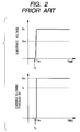
The resistance of the organic film of a portion on
which a bit is recorded is smaller by 100 times or more
than that of a portion on which no bit is formed. For
this reason, if a given constant voltage is applied to
the medium, and the voltage is not a proper value, the
resistance of the voltage-applied portion decreases,
and at the same time, a current flowing through a
resistor RT in the medium portion abruptly increases to
exceed a current threshold IE at which breakdown occurs,
and reaches a saturation current value Isat, as shown
in Fig. 2. As a result, a bit is formed with
breakdown, exhibiting instability in terms of shape and
position.
Furthermore, the error correction function, the
tracking function for a read operation, and the like
must be enhanced because of these problems in a
recording operation, resulting in a heavy load on the
system. In addition, the error rate in a
recording/reproducing operation is high.
SUMMARY OF THE INVENTION
It is, therefore, an object of the present
invention to provide an information recording apparatus
and method which control a bias and a current flowing
through a recording medium in accordance with the local
characteristics of the recording medium, when
information is to be recorded as a bit, so as to
perform a stable recording operation in terms of bit
shape and position.
In order to achieve the above object, there is
provided an information recording apparatus for
recording information by applying a voltage between a
probe and a recording medium, comprising:
wherein when the information is to be recorded,
the charge storage means and the DC power supply are
disconnected from each other by the switch, and the
charges stored in the charge storage means are output
to the probe or the recording medium.
In addition, in order to achieve the above object,
there is provided an information recording method of
recording information by applying a voltage between a
probe and a recording medium, comprising the steps of:
The present invention will be described in detail
in the following embodiment in conjunction with the
accompanying drawings.
BRIEF DESCRIPTION OF THE DRAWINGS
Fig. 1 is a sectional view schematically showing a
bit recording operation;
Fig. 2 is a graph showing a change in
current/voltage as a function of time upon application
of a rectangular pulse;
Fig. 3 is a block diagram showing the arrangement
of an embodiment of the present invention;
Fig. 4 is a circuit diagram showing the schematic
arrangement of a bias applying section;
Fig. 5 is an equivalent circuit for explaining a
pulse applying operation;
Fig. 6 is a graph showing a change in
current/voltage as a function of time in a pulse
applying operation using the present invention; and
Fig. 7 is a circuit diagram showing a
current/voltage conversion circuit in a bit signal
detecting section.
DETAILED DESCRIPTION OF THE PREFERRED EMBODIMENTS
According to the present invention, as described
above, in recording information, the charges stored in
the charge storage means are output to the probe or a
recording medium after the charge storage means is
disconnected from the DC power supply. With this
arrangement, the current flowing in the medium can be
controlled while the bias required to form bits is
applied to the medium, thereby recording information
stably in terms of the shapes and positions of the
bits.
In addition, according to the present invention,
since a voltage can be controlled by using only
capacitors, no complicated circuit system for applying
pulses is required. Assume that in a system designed
to apply a bias from the probe side, a plurality of
probes are prepared, and the same medium can be
accessed by the probes to greatly increase the
transmission rate. Even in this case, since the
arrangement of the system is very simple, the process
load can be reduced in manufacturing probes by a
semiconductor process including micromechanics and the
like. In addition, the cost of each probe can be
reduced, and the mounting density of probes can be
increased.
In an information recording/reproducing operation,
since bits are formed stably in terms of bit shape and
position, the read error rate can be reduced without
using any strong tracking mechanism. In addition, no
redundant bits for error correction are required, and
hence the system load in an encoding/decoding operation
can be reduced. Furthermore, the recording density can
be increased.
The contents of the present invention will be
described in detail next with reference to the
accompanying drawings.
Fig. 3 shows the basic arrangement of the present
invention. Recording information is input to an input
device 111 to be developed as the position information
of a record bit on a medium.
A bias applying section 105 applies a
predetermined voltage to a recording medium 102. A
tunnel current JT is then observed between a probe 101
mounted on a cantilever 103 and the recording medium
102.
The probe 101 is brought close to the recording
medium 102 by coarse and fine adjustment mechanisms
with high precision until the tunnel current JT is
observed, although this process is not shown in the
accompanying drawings. The tunnel current JT is
detected by the probe 101 and then input to a bit
signal detecting section 106, which detects a bit
signal from the current signal.
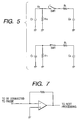
The bit signal detecting section 106 has a
current/voltage conversion circuit, like the one shown
in Fig. 7, at the input portion. The tunnel current JT
is converted into a voltage signal by this circuit, and
the voltage signal is subjected to the subsequent
processing.
Subsequently, for information reproduction, the
detected bit signal is sent to a data extraction
processing section 112. The signal is then reproduced
as information.
The bit signal is a signal obtained by amplifying
the frequency component of the bit of the detected
tunnel current. The data extraction processing section
112 reproduces the recorded information from the bit
detection timing of the signal and the position
information of the probe on the medium.
The reproduced information is sent from the data
extraction processing section 112 to an image data
output section, an audio output section, or an
information processing system for performing processing
in accordance with the information, e.g., using the
information as numerical data for a computer.
The relative positional relationship between the
recording medium 102 and the probe 101 can be changed
by the scanning operation of a movable stage 104.
More specifically, the movable stage 104
incorporates an actuator, and moves the recording
medium in directions (X and Y directions) within a
plane of the recording medium surface in accordance
with driving signals sent from a Y scan signal
generating section 108 and an X scan signal generating
section 109 through amplifiers 110.
Each scan signal generating section (108, 109)
generates a scan signal in accordance with a control
signal output from a scan controlling section 107 on
the basis of control information such as an offset
position, a scan frequency, a main scan (X scan) width,
and a sub-scan (Y scan) width.
The scan controlling section 107 also sends the
probe position information to the input device 111.
The input device 111 then calculates the recording
timing of a bit from the input value, and supplies a
recording control signal to the bias applying section
105.
The operation of the bias applying section 105,
which is a characteristic feature of the present
invention, will be described in detail next with
reference to the accompanying drawings.
Fig. 4 shows the inner arrangement of the bias
applying section 105. The bias applying section 105
includes switches (SW1 and SW2), a charge storage
capacitor CS having a capacitance CS, and a
variable-output power supply VB (having an output VB).
The SW1 and the SW2 are ON/OFF-controlled by a
switch timing control circuit 201 with reference to an
input recording control signal. A bias is applied from
the left output terminal of the SW1 to the medium.
The bias applying section 105 also includes a line
resistor or a limiting resistor RL for determining the
leading edge of an applied pulse.
The operation of this bias applying section 105
will be described in detail next.
First of all, the following steps 1 to 4 indicate
control on the SW1 and the SW2 and the flow of charges.
Assume that both the SW1 and the SW2 are in the
OFF state according to the initial setting.
- step 1:
- The SW2 is turned on; charges are stored
in the charge storage capacitor CS by the
power supply set at the predetermined
bias VB.
- step 2:
- The SW2 is turned off; the power supply
is disconnected.
- step 3:
- The SW1 is turned on; the charge storage
capacitor CS is connected to the medium
when the probe is set at a designated
position (recording position), and a
voltage is applied through the resistor
RL.
- step 4:
- The SW1 is turned off; the charge
storage capacitor CS is disconnected.
The above four steps are cyclically repeated to apply a
bit recording pulse.
The electrical behavior of the system in an actual
pulse applying operation will be described next.
In step 1, charges CSVB are stored in the charge
storage capacitor CS. In step 2, no electrical change
occurs.
At this time, the probe is scanned over the medium
surface to be moved to a recording position.
In step 3, a pulse is actually applied.
This operation will be described with reference to
Fig. 5 which shows an equivalent circuit of the pulse
applying system. Referring to Fig. 5, this circuit has
a capacitance CT corresponding to the sum of the
parasitic capacitances of the medium and other portions
and medium resistors RT0 and RT1. In Fig. 5, the charges
CSVB are stored in the charge storage capacitor CS.
Fig. 6 shows the behaviors of a current and a voltage.
When the SW1 is closed at time T0, some of the charges
in the charge storage capacitor CS start flowing into
the capacitance CT through the resistor RL, and a probe
potential VA rises.
At this time, since the resistor RT0 of the medium
is very large, almost no conduction current flows
through this portion.
When, however, the probe potential VA exceeds a
given threshold voltage VON, which is locally present on
the medium, at time TON, transition of the organic
medium occurs, and an initial high-resistance state RT0
shifts to a low-resistance state RT1. As a result, the
conduction current flowing through this resistor
portion abruptly increases. Since the stored charges
are discharged by this current, the rise in the probe
voltage VA is slowed down.
Although a large current temporarily flows, since
this current value flows in accordance with the probe
voltage VA, no excessive bias is applied. For this
reason, the current value does not reach a threshold IE.
If the upper limit of the variation range of
threshold voltage VON is represented by VM in Fig. 6, VM
is determined by CT and CS:
VM = CSVB/(CS + CT)
According to this equation, VM can be increased by
increasing VB.
With the above operation, a sufficient bias can be
applied regardless of local variations in VON. In
addition, the generated current can be controlled.
As described above, according to the present
invention, biases and pulses are applied to the medium.
However, these biases and pulses can be applied from
the probe side in the same manner as described above by
only changing the output terminal of the circuit in
Fig. 4 from the medium to the probe.
An example of the embodiment of the present
invention will be described next.
In this embodiment, an experiment in a
recording/reproducing operation was conducted by using
the pulse applying mechanism of the present invention.
A polyimide Langmuir-Blodgett (LB) film stacked on
an Au electrode was used as a recording medium, and the
bias applying circuit of the present invention was used
to apply a bias voltage to the medium, thereby
recording information thereon.
As power supply voltage VB in Fig. 4, 10 V was set.
As the capacitance of the charge storage capacitor CS, 5
pF was set. The parasitic capacitance CT was 1 pF or
less.
From these discharging times, the measured pulse
applying time was about 50 µsec. The ON/OFF timings of
the SW1 and the SW2 were set in the switch timing
control circuit 201 in accordance with this measured
time, and a pulse was applied.
In a read operation, the voltage VB was set to a
read voltage of 2.5 V, and a read operation was
designated to the switch timing control circuit 201,
thus closing both the SW1 and the SW2 and applying a DC
bias to the medium.
When character information and image information
were recorded and reproduced with the above settings,
it was confirmed that the error rate was reduced to
1/10 that in the prior art.
When the electrical shapes of the recorded bits
were observed with a scanning tunneling microscope, it
was confirmed that no bit destroying phenomenon had
occurred, and variations in bit size and position were
about 0.1% of the bit size.
As has been described above, according to the
present invention, in recording information, the
charges stored in the charge storage means are output
to the probe or a recording medium after the charge
storage means is disconnected from the DC power supply.
With this arrangement, when a pulse is to be applied, a
bias and a current can be controlled in accordance with
the local characteristics of the medium at the pulse
applying position. This operation allows stable
recording in terms of bit shape and position, and can
greatly decrease the error rate in a
recording/reproducing operation.
In addition, since a voltage can be controlled by
using only the capacitors, no complicated circuit
system for applying pulses is required. Assume that in
a system designed to apply a bias from the probe side,
a plurality of probes are prepared, and the same medium
can be accessed by the probes to greatly increase the
transmission rate. Even in this case, since the
arrangement of the system is very simple, the process
load can be reduced in manufacturing probes by a
semiconductor process including micromechanics and the
like. In addition, the cost of each probe can be
reduced, and the mounting density of probes can be
increased.
In an information recording/reproducing operation,
since bits are formed stably in terms of bit shape and
position, the read error rate can be reduced without
using any strong tracking mechanism. In addition, no
redundant bits for error correction are required, and
hence the system load in an encoding/decoding operation
can be reduced. Furthermore, the recording density can
be increased.