EP0836149A2 - Method and apparatus for reading out dot patterns - Google Patents
Method and apparatus for reading out dot patterns Download PDFInfo
- Publication number
- EP0836149A2 EP0836149A2 EP97307955A EP97307955A EP0836149A2 EP 0836149 A2 EP0836149 A2 EP 0836149A2 EP 97307955 A EP97307955 A EP 97307955A EP 97307955 A EP97307955 A EP 97307955A EP 0836149 A2 EP0836149 A2 EP 0836149A2
- Authority
- EP
- European Patent Office
- Prior art keywords
- array
- detector
- glyphs
- detectors
- glyph
- Prior art date
- Legal status (The legal status is an assumption and is not a legal conclusion. Google has not performed a legal analysis and makes no representation as to the accuracy of the status listed.)
- Granted
Links
- 238000000034 method Methods 0.000 title claims description 23
- 238000013459 approach Methods 0.000 claims abstract description 7
- 238000009826 distribution Methods 0.000 claims description 7
- 238000011144 upstream manufacturing Methods 0.000 claims 1
- 238000003491 array Methods 0.000 abstract description 11
- 230000004044 response Effects 0.000 abstract description 5
- 238000004458 analytical method Methods 0.000 abstract description 4
- 238000001514 detection method Methods 0.000 abstract description 4
- 230000003287 optical effect Effects 0.000 description 6
- 229910021417 amorphous silicon Inorganic materials 0.000 description 3
- 238000005286 illumination Methods 0.000 description 3
- 239000000758 substrate Substances 0.000 description 3
- 229910052751 metal Inorganic materials 0.000 description 2
- 239000002184 metal Substances 0.000 description 2
- 238000012545 processing Methods 0.000 description 2
- 241001270131 Agaricus moelleri Species 0.000 description 1
- VYZAMTAEIAYCRO-UHFFFAOYSA-N Chromium Chemical compound [Cr] VYZAMTAEIAYCRO-UHFFFAOYSA-N 0.000 description 1
- 229910052782 aluminium Inorganic materials 0.000 description 1
- XAGFODPZIPBFFR-UHFFFAOYSA-N aluminium Chemical compound [Al] XAGFODPZIPBFFR-UHFFFAOYSA-N 0.000 description 1
- 239000003990 capacitor Substances 0.000 description 1
- 229910052804 chromium Inorganic materials 0.000 description 1
- 239000011651 chromium Substances 0.000 description 1
- 238000005520 cutting process Methods 0.000 description 1
- 238000013461 design Methods 0.000 description 1
- 230000000694 effects Effects 0.000 description 1
- 239000011521 glass Substances 0.000 description 1
- 238000004519 manufacturing process Methods 0.000 description 1
- 238000012856 packing Methods 0.000 description 1
- 238000002161 passivation Methods 0.000 description 1
- 238000000206 photolithography Methods 0.000 description 1
- 238000003860 storage Methods 0.000 description 1
Images


Classifications
-
- G—PHYSICS
- G06—COMPUTING; CALCULATING OR COUNTING
- G06K—GRAPHICAL DATA READING; PRESENTATION OF DATA; RECORD CARRIERS; HANDLING RECORD CARRIERS
- G06K7/00—Methods or arrangements for sensing record carriers, e.g. for reading patterns
- G06K7/10—Methods or arrangements for sensing record carriers, e.g. for reading patterns by electromagnetic radiation, e.g. optical sensing; by corpuscular radiation
- G06K7/14—Methods or arrangements for sensing record carriers, e.g. for reading patterns by electromagnetic radiation, e.g. optical sensing; by corpuscular radiation using light without selection of wavelength, e.g. sensing reflected white light
- G06K7/1404—Methods for optical code recognition
- G06K7/1408—Methods for optical code recognition the method being specifically adapted for the type of code
- G06K7/143—Glyph-codes
-
- G—PHYSICS
- G06—COMPUTING; CALCULATING OR COUNTING
- G06K—GRAPHICAL DATA READING; PRESENTATION OF DATA; RECORD CARRIERS; HANDLING RECORD CARRIERS
- G06K7/00—Methods or arrangements for sensing record carriers, e.g. for reading patterns
- G06K7/10—Methods or arrangements for sensing record carriers, e.g. for reading patterns by electromagnetic radiation, e.g. optical sensing; by corpuscular radiation
- G06K7/10544—Methods or arrangements for sensing record carriers, e.g. for reading patterns by electromagnetic radiation, e.g. optical sensing; by corpuscular radiation by scanning of the records by radiation in the optical part of the electromagnetic spectrum
- G06K7/10712—Fixed beam scanning
- G06K7/10722—Photodetector array or CCD scanning
Definitions
- the present invention relates to the detection of dot pattems.
- Glyphs are an example of dot pattems and can be visually non-obtrusive encodings of information in the gray scale portions of pictures, drawings, logos, forms, and the like. More specifically, printers typically print black and white images by applying a series of dots of ink or toner to the print medium.
- a 600 dpi printer for example, prints up to 600 dots per inch (240 dots per centimeter) in each horizontal line and prints 600 lines per inch (240 lines per centimeter) vertically. That is, each square inch (6.45cm 2 ) contains a 600x600 grid of pixels. Black can be printed by placing a black dot in every available pixel and white by leaving the print medium white.
- Gray scales are depicted by adjusting the optical density of the applied ink or toner. For example, a small fraction of the pixels contain dots to depict pale gray, a large percentage for medium gray, etc.
- Glyphs rearrange the dot patterns for a given gray shade in order to encode information. Rather than applying the dots for a given gray scale randomly, the dots are placed in preselected groupings of the same optical density to encode information.
- a 5x5 array of pixels is dedicated to each glyph. Three dots on a diagonal going down from left to right through the center of the pixel array define a glyph of one polarity and three dots going down from right to left through the center of the array define a glyph of the opposite polarity. These two polarity glyphs are typically used to encode binary information.
- Binary information can be encoded onto the print medium by printing lines of these 5x5 arrays. Such lines of glyphs have a uniform gray scale density and appear as gray bands which may be incorporated into logos, letterhead, borders, and the like. Such glyphs can also be encoded more subtly into portions of the image which already have this same gray scale level.
- the glyphs may be utilized to encode an identification of the document, its date of printing, an identification of the printer on which it was printed, and the like. Glyphs may also be used in security applications to encode digital information into background or foreground gray scale regions of an image.
- a passport image can be glyph encoded to carry a binary identification of the passport number, the name of the passport owner, a description of the person, or the like.
- the invention addresses the above problems in reading and decoding glyphs and other dot patterns. Specifically, the invention addresses the memory and computation requirements of scanning an entire page to generate a bit-map and analyzing the bit-map.
- the invention provides techniques that alleviate these problems. Some of the techniques use arrays of analog detectors to read out dot patterns. Others approximate an image by forming a parametric model within each sensor element in an array, sensing signals from the sensor elements, determining parameters of the model from the signals, and using the parameters to approximate intensity distribution of light.
- the techniques are advantageous because they can identify and read glyphs in real time, without performing software analysis of an image. Some of the techniques can accurately distinguish glyphs from random dots and other dot patterns. Some techniques can read out entire lines of glyphs simultaneously, and can predict and identify the locations of lines of glyphs.
- a method of reading out dot patterns comprising: (A) receiving an image with an array of detectors, the image including dot patterns; (B) operating each detector to provide, when receiving one of the dot patterns, an analog signal indicating a type of the dot pattem; and (C) reading out the analog signals from the detectors.
- apparatus for reading out dot patterns comprising: an array of detectors for receiving images that include dot patterns; each detector providing, when receiving one of the dot patterns, an analog signal indicating a type of the dot pattem; and readout means for reading out the analog signals from the detectors.
- a method of approximating an image projected onto an array of sensor elements comprising: forming a parametric model for the spatial intensity distribution within a sensor element, said sensor element being responsive to its own internal spatial variation of intensity; sensing signals from said sensor element; determining the parameters of said model from said sensor signals; and using said parameters obtained from an array of said sensor elements to approximate the intensity distribution of light radiated onto the array.
- the invention can be implemented to detect glyphs on a print medium with an optical reader.
- the optical reader can include an array of analog pattern sensitive detectors.
- An image on the print medium can be illuminated such that light from the image strikes the array, and the array can discriminate glyphs from the remainder of the image and generate analog signals indicative of the glyphs.
- An analog-to-digital converter can convert the analog output into a digital signal in accordance with the detected glyphs without performing software analysis of the image.
- the glyphs can each have one of two orientations, and an analog signal of a first polarity can be generated in response to one orientation, while an analog signal of a second polarity can be generated in response to the other orientation.
- the analog signals can then be converted into binary signals.
- the glyphs can extend along diagonals, and the detectors can be crossed detectors differentially interconnected such that glyphs with a different orientations produce differently signed analog signals, one positive and one negative.
- Each detector can have four lobes, each a light sensitive PIN diode, the four being symmetrically disposed or including two oppositely disposed diagonal pairs.
- Two diagonal diodes can be electrically connected by a first electrode surface, providing anodes, and the other two diagonal diodes can be electrically connected by a second electrode surface, providing cathodes.
- the first and second electrode surfaces can be interconnected, but with a positive voltage bias connected opposite the first electrode surface, providing cathodes, and with a negative voltage bias connected opposite the second electrode surface, providing anodes.
- a gated transistor can be connected with the first and second electrode surfaces.
- a centroid of light falling on each detector can be determined and its magnitude can be analyzed to identify glyphs and glyph polarities.
- Each detector can have a substrate, a first pair of electrodes supported on the substrate, a PIN diode mounted on the first pair of electrodes, and a pair of collection electrodes mounted on the PIN diode.
- each detector can include a vertical PIN diode and a plurality of electrodes on opposite faces of the diode.
- a glyph reading system that reads glyphs with three dots disposed along one of two orthogonal, diagonal directions can include three light sensitive bands which are spaced apart such that when a center pixel of the glyph is centered on the center band, the outer bands are disposed beyond the glyph.
- the center band can be opposite biased relative to the outer bands and their outputs can be interconnected such that the output of the bands exceeds a preselected threshold when a line of glyphs is centered under the central band.
- the detectors can include a plurality of arrays of interleaved pattern sensitive detectors, and the arrays can be offset from each other by a glyph or contact thereof; the array most closely aligned with the glyphs passing thereunder can read out the glyphs.
- a sensing device for sensing an image can include a plurality of sensor elements, each sensing its own intra-sensor spatial variation of intensity.
- the sensor elements can be organized into an array having signal outputs that approximate at least a portion of an image with subsensor accuracy.
- the invention can be embodied in a sensing device for sensing an image where the sensing device includes a plurality of sensor elements, each of which senses its own intra-sensor spatial variation of intensity.
- the sensor elements are organized into an array which produces signal outputs which approximate at least a portion of the image with subsensor accuracy.
- the invention can also be embodied in a glyph detection system in which a print medium containing an image is passed below an optical reader.
- the optical reader includes an array of analog pattern sensitive detectors which detect glyphs and output analog signals indicative thereof.
- the invention can also be embodied in a method of approximating an image projected onto an array of sensor elements.
- a parametric model is formed for the spatial intensity distribution within a sensor element, which sensor element is responsive to its own internal spatial variation of intensity. Signals from the sensor element are sensed. The parameters of the model are determined from the sensor signals. The parameters obtained from an array of the sensor elements are used to approximate the intensity distribution of the light radiated onto the array.
- the invention can also be embodied in a method of detecting glyphs.
- a print medium on which a glyph containing image is printed is fed past an analog photosensitive detector array.
- the image is illuminated such that light is reflected from the image to the analog photosensitive detector array.
- the analog photosensitive detector array With the analog photosensitive detector array, the glyphs are discriminated from a remainder of the image and analog signals indicative of the glyphs are generated. In this manner, the glyphs are read out directly at the detector array without computer analysis of the image.
- an image is divisible into a multiplicity of pixel arrays, such as the illustrated 5x5 pixel array 10.
- any of the 25 pixels can contain a black dot and any of the 25 pixels can be left white.
- a glyph 12 is made up of three dots disposed on a diagonal through the center pixel. Alternately, the glyph can pass through the center pixel of the array with the opposite slope to make an opposite polarity glyph 14.
- glyphs 12 and 14 are used to represent binary 1's and 0's. Lines of glyphs can be printed in lines across portions of an image.
- a sheet of print paper or other print medium containing such lines of glyphs is moved at a controlled speed past a light source and one or more arrays of light sensitive glyph detectors.
- the glyph detector arrays output analog signals from the read glyphs which can be converted immediately to binary digital signals.
- the detector array is clocked for read out in accordance with the feed rate of the paper and the interglyph line intervals.
- a glyph detector 20 of the illustrated embodiment has two pairs of optically sensitive elements, particularly photodiodes, including a pair 22a, 22b which are sized to fit over the end two dots of the glyph 12 and a pair 24a, 24b sized and dimensioned to overlay the end two dots of glyph 14. It is to be appreciated that the exact spacing, size, and placement of the photosensitive elements conform to the dimensions and configuration of the selected glyphs.
- the photodiodes 22a, 22b each include a PN junction or PIN 26 disposed between interconnected upper electrodes 28 and lower electrodes 30.
- the second pair of photodiodes 24a, 24b also include junction 32 sandwiched between upper electrodes 34 and interconnected lower electrodes 36.
- the upper electrodes 28 of photodiodes 22a, 22b are connected by way of a via 38 to the lower electrodes 36 of photodiodes 24a, 24b. These interconnected electrodes are further connected to an output transistor 40.
- the lower electrodes 30 of diodes 22a, 22b are connected with a positive voltage source 42.
- Upper electrodes 34 of diodes 24a, 24b are connected with a negative voltage source 44. More generally, source 44 is at least several volts less than source 42.
- the supplies could be monopolar, e.g., +5V and 0V, or 0V and -5V.
- FIGURE 5 a single pixel wide diagonal edge or line cutting through a field of white could be misread as a glyph.
- the embodiment of FIGURE 5 adds a pair of photodiodes 46a, 46b in line with photodiodes 22a, 22b. Diodes 46a, 46b detect whether a line of dots detected by 22a, 22b is more than three dots long. By making diodes 46a, 46b of opposite polarity from diodes photodiodes 22a, 22b and adding their outputs, the maximum signal is produced by three dots.
- a pair of photodiodes 48a, 48b are disposed in line with photodiodes 24a, 24b to determine whether any line of dots passing below photodiodes 24a, 24b is more than three dots long. In this manner, glyphs are differentiated from diagonal lines.
- glyphs are detected using a moment-sensitive photosensor 50.
- the moment sensitive photodetector includes a vertical PIN diode 52 with resistance layers 54, 56 on opposite surfaces.
- Four straight resistive contact strips 58a, 58b, 58c, 58d with constant conductivity along their length L frame the lower resistance layer.
- four tapered resistive strips 60a, 60b, 60c, 60d frame the top resistive surface.
- a position sensitive detector of this nature produces output currents that vary in accordance with the portions of the resistive layer 54 which are illuminated and not illuminated.
- the tapered electrodes effectively sum the photogenerated currents with weighting factors proportional to the square of the distance of each current source from a particular edge while the straight electrodes weight the current linearly with the distance of the source from a particular edge.
- the first moment is effectively a balance point or center of mass of the light spot(s).
- the second moment weights the off center light more heavily than the on center.
- the size of the photosensitive area is sized to match the size of a glyph 12.
- the light is balanced in the x-direction and the light is balanced in the y-direction (although the light is not balanced between the x and y-directions). This effective balance is sensed by the first moment.
- the second moment weights the effect of the off center dots more heavily, providing an indication of the orientation.
- lateral photodiodes are utilized similar to a pattern sensitive detector.
- a vertical PIN diode 70 has an insulating layer 72 on one face and a resistive layer 74 on the opposite face.
- Conductive leads 76a, 76b, 76c, and 76d are mounted on insulating layer 72.
- Matching resistive electrodes 78a, 78b, 78c, and 78d are mounted on the resistive layer.
- the conductive leads and resistive electrodes are connected by vias 80a, 80b at one corner. At the opposite corner, the conductive leads are connected to a pair of differential amplifiers 82a, 82b.
- This detector uses the resistive electrodes as a current divider with the two sides of the square sensor monitored in tandem.
- the light induced photo charge flows in the resistive layer 74 to the edges which are held close to ground.
- the edge current then divides in the resistance electrodes and flows to the differential amplifiers 82a, 82b or to storage capacitors.
- a glyph breaks the symmetry of the cell. When a glyph is centered with a vertical orientation, the output is a maximum voltage of a first polarity and when the glyph is located horizontally, the output is an opposite polarity maximum.
- the pattern sensitive detectors of the embodiment of FIGURES 6, 7, or 8 and the embodiment of FIGURES 9 and 10 are both sensitive to glyphs which are disposed parallel to the rectangular side walls.
- the detectors are rotated ⁇ /4 rad (45°)as illustrated in FIGURE 11.
- the detectors are arranged in rectangular arrays of appropriate packing and spacing to match the size and spacing of the glyphs or image of glyphs projected onto detectors. The rows of detectors are spaced with the same periodicity as the glyphs.
- each row of glyphs centers simultaneously on one of the rows of detectors and intermediate rows of detectors detect pure white.
- the sensing of pure white by alternate rows of detectors provides a double-check that glyphs are, in fact, being detected. If the glyphs are offset by half a period in the row direction, then the glyphs will align with the alternate rows of detectors.
- the outputs of the alternate detector rows can be weighted to optimally identify the glyphs.
- the interpreted outputs can be asynchronously loaded into a binary buffer to scan out a row of glyph data.
- the glyphs are sensed with a shaped position sensor 90.
- the shaped position sensor glyph detector 90 is fabricated by applying a metal layer 92, such as chromium, on a low cost substrate such as glass. The metal layer is patterned to form the bottom collection electrode.
- a thin, typically 30nm layer 94 of heavily doped amorphous silicon (p-type in one embodiment) is deposited followed by a thicker intrinsic layer 96, typically about 500nm, and finally a thin, typically 30nm layer 98 of heavily n-type doped amorphous silicon.
- a semi-transparent contact resistive layer 100 is deposited. The layers of amorphous silicon and the semi-transparent contact are patterned using photolithography. A passivation layer (not shown) is deposited and holes are cut in this layer to expose the top semi-transparent contact.
- Two contacting electrodes 102 typically aluminum, are photolithographically fabricated to be in electrical contact with the semi-transparent resistive layer 100.
- a row of the two electrode glyph detectors are mounted at a common angle with a line 104 of glyphs of a first polarity.
- Currents I 1 and I 2 in the electrodes 102 are measured as the glyph pattern crosses the detector.
- the sum of the two currents I 1 + I 2 is proportional to the total light falling on the detector.
- one shaped position sensor glyph detector measures glyphs located at more than one location through the examination of the quantity Î. One can also determine whether a part of the glyph lies within the detector by the position of the centroid. The shaped position sensor in this manner detects glyphs which are offcenter from the detector, allowing a less dense array of detectors to be utilized.
- This arrangement is advantageous in that it does not require lateral registration of the sensor with the glyph. This avoids complex switching circuits or a dense array of sensors.
- One detector can detect more than one glyph, lowering the detector density requirements.
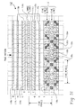
- detectors of the first embodiment of FIGURES 1-4 are also amenable to fabrication into an array 110.
- the opposing pairs of lobes are interlaced to create a row of interlaced or overlapping detectors.
- the rows of detectors are preceded in the feed direction by a predetector array 112 which determines the centers of rows of approaching glyphs.
- the predetector array 112 includes three sets of electrodes. In each set, a central light sensitive sensor 116a, 116b, and 116c extends the length of a line. A pair of light sensitive side detectors 118a, 118b, and 118c, and 120a, 120b, or 120c extend parallel to the first predetector electrode, but offset by two and 3/8 pixels on each side (in one embodiment). The side electrodes 118, 120 are also half of the width of the central electrode 116 so that the sum of their area equals that of the central electrode. The output of the corresponding side sensors 118, 120 are connected together and summed with the corresponding central sensors 116 in a manner similar to that illustrated in FIGURES 2 and 3.
- the outputs of 116a, 118a, 120a are generated by the summed current at the common nodes and represent the difference between the light falling on the central sensor and the sum of the corresponding side sensors.
- side electrodes 118, 120 view the white pixels on either edge of the 5x5 pixel glyph. That is, the black dots under electrode 116 produce a minimal illumination and the absence of dots below electrodes 118, 120 produce a maximum illumination output.
- the difference exceeds a predetermined threshold as the center of the glyph passes directly under electrode 116a.
- the three sets of detectors are offset by one pixel.
- the summed output 122a is compared 124 with the outputs 122b and 122c and with a threshold 126.
- the three comparisons are ANDed 128 to produce a signal indicating a row of glyphs centered under electrode 116a.
- the center electrode 116a is centered at any one of 5 pixels, the dimension of a glyph, or another known distance, from the center of the electrode array 110. In this manner, the validity signal indicates when one can expect to find a line of glyphs centered on the central row of the electrode array 110.
- the detector array 110 includes five sets of interleaved detectors with positive polarity cells +a, +b, +c, +d, and +e on one diagonal and opposite polarity cells -a, -b, -c, -d and -e on the other diagonal.
- Each detector with crossed positive and negative polarity electrodes is spaced by the dimension of one glyph, 5 pixels in the preferred embodiment, from the next like detector of the same set.
- the sets are staggered, by 1 pixel in the illustrated embodiment, to detect whether the glyphs are aligned most closely to any one of five lateral positions.
- the center pixel of the glyph will fall under detectors 130a; if the glyphs are offset by half a pixel to the right, then the center will fall under detectors 130b; if the glyphs are offset by a full pixel, the centers will fall under detectors 130c.
- the outputs of the sets a, b, c, d, e of the detector array 130a-130e are analyzed to determine the horizontal center of the glyphs, hence which of the detectors a, b, c, d, e should be activated to read the glyphs. More specifically, the output of sets a and b are compared 140 and the output of sets c and d are compared 142. The comparison controls switches 144, 146 which switch the larger of a and b and the larger of c and d to a comparator 148.
- the comparator 148 controls a switch 150 which channels the largest output to a comparator 152 that compares the largest of a, b, c, and d with input e.
- the output of comparator 152 controls a switch 154 that connects the largest of a, b, c, d, and e with a comparator 156 for comparison with a threshold which shows that a row of glyphs is under the array.
- the outputs for the four comparators create a four-bit binary number indicating which of sets a, b, c, d, or e is to be read.
- the four bit binary indication of the centered detector array controls a switch 158 which switches the signals from the selected array to parallel output lines.
- glyphs may be encoded in other than a binary manner, for example, line glyphs of the type described above may be disposed at ⁇ /4 rad (45°) intervals to produce an output which can take on any one of four states to carry two bits worth of information.
- the invention could further be implemented with dot patterns other than glyphs such as marks or characters, and could also be implemented with distinguishing features of dot patterns other than orientation.
- Each dot pattern could denote one of more than two values--in general, the number of different types of dot patterns that can be discriminated determines the amount of information conveyed by each dot pattern.
- dot patterns from printed images as the images move past an array
- the invention could read out dot patterns from any other type of image that can include dot patterns, and the image could be provided without moving a print medium past an array, such as by projecting an image onto the array or by moving the array past the print medium.
- Any appropriate characteristic of an analog signal could be used to indicate the type of a dot pattern, not just polarity or magnitude.
Abstract
Description
Claims (10)
- A method of reading out dot patterns, the method comprising:(A) receiving an image with an array (104; 110) of detectors (20; 50; 90; 130a, 130b, 130c, 130d, 130e), the image including dot patterns;(B) operating each detector (20; 50; 90; 130a, 130b, 130c, 130d, 130e) to provide, when receiving one of the dot patterns, an analog signal indicating a type of the dot pattern; and(C) reading out the analog signals from the detectors (20; 50; 90; 130a, 130b, 130c, 130d, 130e).
- The method as set forth in claim 1 in which the dot patterns include first and second types and in which (B) comprises operating each detector (20; 50; 90; 130a, 130b, 130c, 130d, 130e) to provide an analog signal having a first characteristic when receiving a dot pattern of the first type and to provide an analog signal having a second characteristic when receiving a dot pattern of the second type; the method further comprising:
(D) converting the analog signals into binary signals. - The method as set forth in claim 1 in which each detector (50) provides an analog signal that includes output currents that vary in accordance with portions of the detector (50) that are illuminated; the method further comprising:(E) determining a moment of the light falling on each detector (50) from the output currents; and(F) determining the type indicated by the analog signal from the moment.
- Apparatus for reading out dot patterns, comprising:an array (104; 110) of detectors (20; 50; 90; 130a, 130b, 130c, 130d, 130e) for receiving images that include dot pattems; each detector (20; 50; 90; 130a, 130b, 130c, 130d, 130e) providing, when receiving one of the dot patterns, an analog signal indicating a type of the dot pattern; andreadout means (40; 82a, 82b; 102; 140-158) for reading out the analog signals from the detectors (20; 50; 90; 130a, 130b, 130c, 130d, 130e).
- Apparatus as set forth in claim 4 in which the images include dot patterns in lines, the apparatus further comprising:motion means for moving images along a path past the array (104; 110) of detectors (20; 50; 90; 130a, 130b, 130c, 130d, 130e); anda predetector array (112) of photosensitive elements (116a, 116b, 116c, 118a, 118b, 118c, 120a, 120b, 120c) for detecting the approach of a line of dot pattems; the predetector array (112) being disposed upstream from the array (104; 110) of detectors (20; 50; 90; 130a, 130b, 130c, 130d, 130e).
- Apparatus as set forth in claim 4 or claim 5, wherein a detector (20) has four symmetrically disposed photodiodes (22a, 22b, 24a, 24b), with oppositely disposed pairs of photodiodes being connected electrically in parallel.
- Apparatus as set forth in claim 4 or claim 5, wherein a detector (50) includes:a vertical PIN diode (52);a bottom resistance layer (56) connected with one surface of the PIN diode (52) and a top resistance layer (54) connected with an opposite surface of the PIN diode (52);an array of top contacts electrically connected with the top resistance layer (54), the top contacts including four tapered conductive resistance contacts (60a, 60b, 60c, 60d);an array of bottom contacts including four linear conductive contacts (58a, 58b, 58c, 58d).
- Apparatus as set forth in claim 4 or claim 5, wherein a detector includes:a vertical PIN diode (70);a resistance layer (74) disposed on one surface of the vertical PIN diode (70) and an insulating layer (72) disposed on an opposite surface of the vertical PIN diode (70);a top conductive lead array (76a, 76b, 76c, 76d) mounted on the insulating layer (72), the top conductive leads including a first lead (76a, 76b) which extends substantially along two sides of a square and a second lead (76c, 76d) which extends along two opposite sides of the square;a bottom resistive electrical lead array (78a, 78b, 78c, 78d) including a first bottom electrical lead (78a, 78b) extending substantially along two sides of a square and a second bottom electrical lead (78c, 78d) extending along two opposite sides of the square;electrical interconnections (80a, 80b) for interconnecting ends of the top and bottom leads adjacent one corner of the squares;differential amplifiers (82a, 82b) connected with free ends of the top and bottom leads (76a, 76b, 76c, 76d, 78a, 78b, 78c, 78d) adjacent an opposite end of the squares.
- Apparatus as set forth in claim 4 or claim 5, wherein a detector (90) includes:PIN layers (94, 96, 98);a resistance layer (100) disposed on one surface of the PIN layers (94, 96, 98) and a bottom collection electrode (92) disposed on an opposite surface of the PIN layers (94, 96, 98); andtop conductive electrodes (102) mounted on the resistance layer (100), the top conductive electrodes (102) including first and second substantially parallel electrodes shaped and oriented for providing current that depends on orientation of dot patterns.
- A method of approximating an image projected onto an array (104; 110) of sensor elements (20; 50; 90; 130a, 130b, 130c, 130d, 130e), said method comprising:forming a parametric model for the spatial intensity distribution within a sensor element (20; 50; 90; 130a, 130b, 130c, 130d,130e), said sensor element (20; 50;90; 130a, 130b, 130c, 130d, 130e) being responsive to its own internal spatial variation of intensity;sensing signals from said sensor element (20; 50; 90; 130a, 130b, 130c, 130d, 130e);determining the parameters of said model from said sensor signals; andusing said parameters obtained from an array (104; 110) of said sensor elements (20; 50; 90; 130a, 130b, 130c, 130d, 130e) to approximate the intensity distribution of light radiated onto the array (104; 110).
Applications Claiming Priority (2)
| Application Number | Priority Date | Filing Date | Title |
|---|---|---|---|
| US08/728,654 US5864127A (en) | 1996-10-10 | 1996-10-10 | Analog glyph detector and detector arrays |
| US728654 | 2003-12-05 |
Publications (3)
| Publication Number | Publication Date |
|---|---|
| EP0836149A2 true EP0836149A2 (en) | 1998-04-15 |
| EP0836149A3 EP0836149A3 (en) | 2002-01-02 |
| EP0836149B1 EP0836149B1 (en) | 2005-01-05 |
Family
ID=24927744
Family Applications (1)
| Application Number | Title | Priority Date | Filing Date |
|---|---|---|---|
| EP97307955A Expired - Lifetime EP0836149B1 (en) | 1996-10-10 | 1997-10-08 | Method and apparatus for reading out dot patterns |
Country Status (4)
| Country | Link |
|---|---|
| US (1) | US5864127A (en) |
| EP (1) | EP0836149B1 (en) |
| JP (1) | JP4152463B2 (en) |
| DE (1) | DE69732168T2 (en) |
Cited By (3)
| Publication number | Priority date | Publication date | Assignee | Title |
|---|---|---|---|---|
| EP1720118A2 (en) * | 2005-05-06 | 2006-11-08 | Secure Edge S.r.l. | High-density two-dimensional graphic code, and coding system and decoding system based on said code |
| WO2008049550A2 (en) * | 2006-10-26 | 2008-05-02 | Man Roland Druckmaschinen Ag | Apparatus, method and process for the stochastic marking and tracking of printed products |
| ITBO20110016A1 (en) * | 2011-01-20 | 2012-07-21 | Walter Ritelli | CODE TWO-DIMENSIONAL GRAPHIC WITH MATRIX |
Families Citing this family (16)
| Publication number | Priority date | Publication date | Assignee | Title |
|---|---|---|---|---|
| SE516522C2 (en) * | 1999-05-28 | 2002-01-22 | Anoto Ab | Position determining product for digitization of drawings or handwritten information, obtains displacement between symbol strings along symbol rows when symbol strings are repeated on symbol rows |
| SE517445C2 (en) | 1999-10-01 | 2002-06-04 | Anoto Ab | Position determination on a surface provided with a position coding pattern |
| US6367909B1 (en) | 1999-11-23 | 2002-04-09 | Xerox Corporation | Method and apparatus for reducing drop placement error in printers |
| US6785011B1 (en) | 2000-03-16 | 2004-08-31 | Lexmark International, Inc | Optical sensor arrangement for start of scan detection and improved vertical beam alignment range |
| US7143952B2 (en) * | 2000-03-21 | 2006-12-05 | Anoto Ab | Apparatus and methods relating to image coding |
| US6697094B2 (en) | 2001-05-14 | 2004-02-24 | Lexmark International, Inc. | Method and apparatus for locating the process postion of a scan line in an electrophotographic machine |
| AU2003220269A1 (en) | 2002-03-14 | 2003-09-29 | Contentguard Holdings, Inc. | Method and apparatus for processing usage rights expressions |
| US20030229593A1 (en) * | 2002-03-14 | 2003-12-11 | Michael Raley | Rights expression profile system and method |
| JP4242796B2 (en) * | 2004-03-12 | 2009-03-25 | パナソニック株式会社 | Image recognition method and image recognition apparatus |
| US8316068B2 (en) | 2004-06-04 | 2012-11-20 | Telefonaktiebolaget Lm Ericsson (Publ) | Memory compression |
| US20100231404A1 (en) * | 2006-09-22 | 2010-09-16 | Koninklijke Philips Electronics N V | Illumination system having an array of light sources |
| US7688947B2 (en) * | 2006-10-17 | 2010-03-30 | Varian Medical Systems, Inc. | Method for reducing sensitivity modulation and lag in electronic imagers |
| JP5557419B2 (en) * | 2007-10-17 | 2014-07-23 | スパンション エルエルシー | Semiconductor device |
| DE102008017168A1 (en) * | 2008-04-02 | 2009-10-08 | Crossmedia Solution Gmbh & Co. Kg | Method for storing and reading data |
| US7991153B1 (en) | 2008-08-26 | 2011-08-02 | Nanoglyph, LLC | Glyph encryption system and related methods |
| KR101172185B1 (en) * | 2010-08-19 | 2012-08-07 | 주식회사 에이스테크놀로지 | N-port feeding system having a structure in which patterns are divided with in parallel and feeding element included in the same |
Citations (8)
| Publication number | Priority date | Publication date | Assignee | Title |
|---|---|---|---|---|
| WO1989006017A1 (en) * | 1987-12-22 | 1989-06-29 | Drexler Technology Corporation | Method for reading data pages on a data surface |
| EP0469868A2 (en) * | 1990-07-31 | 1992-02-05 | Xerox Corporation | Binary image processing for decoding self-clocking glyph shape codes |
| US5245165A (en) * | 1991-12-27 | 1993-09-14 | Xerox Corporation | Self-clocking glyph code for encoding dual bit digital values robustly |
| US5319182A (en) * | 1992-03-04 | 1994-06-07 | Welch Allyn, Inc. | Integrated solid state light emitting and detecting array and apparatus employing said array |
| US5369261A (en) * | 1992-02-12 | 1994-11-29 | Shamir; Harry | Multi-color information encoding system |
| EP0649074A1 (en) * | 1993-10-18 | 1995-04-19 | Xerox Corporation | A system and method to measure and accrue copyright royalties |
| US5521372A (en) * | 1993-12-22 | 1996-05-28 | Xerox Corporation | Framing codes for robust synchronization and addressing of self-clocking glyph codes |
| EP0736835A2 (en) * | 1995-04-06 | 1996-10-09 | ROLLS-ROYCE plc | Process and apparatus for reading a dot matrix code marking on an article |
Family Cites Families (12)
| Publication number | Priority date | Publication date | Assignee | Title |
|---|---|---|---|---|
| US4716438A (en) * | 1986-11-17 | 1987-12-29 | Xerox Corporation | High speed electronic reprographic/printing machine |
| US4786940A (en) * | 1986-11-17 | 1988-11-22 | Xerox Corporation | Data handling and archiving system |
| US5128525A (en) * | 1990-07-31 | 1992-07-07 | Xerox Corporation | Convolution filtering for decoding self-clocking glyph shape codes |
| US5315098A (en) * | 1990-12-27 | 1994-05-24 | Xerox Corporation | Methods and means for embedding machine readable digital data in halftone images |
| US5278400A (en) * | 1991-08-19 | 1994-01-11 | Xerox Corp | Multiple threshold encoding of machine readable code |
| US5221833A (en) * | 1991-12-27 | 1993-06-22 | Xerox Corporation | Methods and means for reducing bit error rates in reading self-clocking glyph codes |
| US5449896A (en) * | 1993-12-22 | 1995-09-12 | Xerox Corporation | Random access techniques for use with self-clocking glyph codes |
| US5449895A (en) * | 1993-12-22 | 1995-09-12 | Xerox Corporation | Explicit synchronization for self-clocking glyph codes |
| US5453605A (en) * | 1993-12-22 | 1995-09-26 | Xerox Corporation | Global addressability for self-clocking glyph codes |
| US5513264A (en) * | 1994-04-05 | 1996-04-30 | Metanetics Corporation | Visually interactive encoding and decoding of dataforms |
| US5576532A (en) * | 1995-01-03 | 1996-11-19 | Xerox Corporation | Interleaved and interlaced sync codes and address codes for self-clocking glyph codes |
| US5710874A (en) * | 1995-10-25 | 1998-01-20 | Xerox Corporation | System for managing printing system memory with machine readable code |
-
1996
- 1996-10-10 US US08/728,654 patent/US5864127A/en not_active Expired - Lifetime
-
1997
- 1997-10-08 EP EP97307955A patent/EP0836149B1/en not_active Expired - Lifetime
- 1997-10-08 DE DE69732168T patent/DE69732168T2/en not_active Expired - Lifetime
- 1997-10-13 JP JP27880897A patent/JP4152463B2/en not_active Expired - Fee Related
Patent Citations (8)
| Publication number | Priority date | Publication date | Assignee | Title |
|---|---|---|---|---|
| WO1989006017A1 (en) * | 1987-12-22 | 1989-06-29 | Drexler Technology Corporation | Method for reading data pages on a data surface |
| EP0469868A2 (en) * | 1990-07-31 | 1992-02-05 | Xerox Corporation | Binary image processing for decoding self-clocking glyph shape codes |
| US5245165A (en) * | 1991-12-27 | 1993-09-14 | Xerox Corporation | Self-clocking glyph code for encoding dual bit digital values robustly |
| US5369261A (en) * | 1992-02-12 | 1994-11-29 | Shamir; Harry | Multi-color information encoding system |
| US5319182A (en) * | 1992-03-04 | 1994-06-07 | Welch Allyn, Inc. | Integrated solid state light emitting and detecting array and apparatus employing said array |
| EP0649074A1 (en) * | 1993-10-18 | 1995-04-19 | Xerox Corporation | A system and method to measure and accrue copyright royalties |
| US5521372A (en) * | 1993-12-22 | 1996-05-28 | Xerox Corporation | Framing codes for robust synchronization and addressing of self-clocking glyph codes |
| EP0736835A2 (en) * | 1995-04-06 | 1996-10-09 | ROLLS-ROYCE plc | Process and apparatus for reading a dot matrix code marking on an article |
Cited By (8)
| Publication number | Priority date | Publication date | Assignee | Title |
|---|---|---|---|---|
| EP1720118A2 (en) * | 2005-05-06 | 2006-11-08 | Secure Edge S.r.l. | High-density two-dimensional graphic code, and coding system and decoding system based on said code |
| EP1720118A3 (en) * | 2005-05-06 | 2007-11-21 | Secure Edge S.r.l. | High-density two-dimensional graphic code, and coding system and decoding system based on said code |
| US7546958B2 (en) | 2005-05-06 | 2009-06-16 | Secure Edge S.R.L. | High-density two-dimensional graphic code, and coding system and decoding system based on said code |
| WO2008049550A2 (en) * | 2006-10-26 | 2008-05-02 | Man Roland Druckmaschinen Ag | Apparatus, method and process for the stochastic marking and tracking of printed products |
| WO2008049550A3 (en) * | 2006-10-26 | 2008-07-31 | Roland Man Druckmasch | Apparatus, method and process for the stochastic marking and tracking of printed products |
| ITBO20110016A1 (en) * | 2011-01-20 | 2012-07-21 | Walter Ritelli | CODE TWO-DIMENSIONAL GRAPHIC WITH MATRIX |
| WO2012098508A1 (en) * | 2011-01-20 | 2012-07-26 | Ritelli Walter | A bidimensional graphic matrix code |
| US9202155B2 (en) | 2011-01-20 | 2015-12-01 | Walter Ritelli | Bidirectional graphic matrix code |
Also Published As
| Publication number | Publication date |
|---|---|
| DE69732168T2 (en) | 2005-06-02 |
| US5864127A (en) | 1999-01-26 |
| JP4152463B2 (en) | 2008-09-17 |
| JPH10171915A (en) | 1998-06-26 |
| EP0836149A3 (en) | 2002-01-02 |
| DE69732168D1 (en) | 2005-02-10 |
| EP0836149B1 (en) | 2005-01-05 |
Similar Documents
| Publication | Publication Date | Title |
|---|---|---|
| US5864127A (en) | Analog glyph detector and detector arrays | |
| US4724307A (en) | Marked card reader | |
| US4797544A (en) | Optical scanner including position sensors | |
| US4710963A (en) | Apparatus for sensing the condition of a document | |
| US4516264A (en) | Apparatus and process for scanning and analyzing mail information | |
| US20070154073A1 (en) | Swipe imager with multiple sensing arrays | |
| TWI274897B (en) | Optical positioning device resistant to speckle fading | |
| EP1182604A1 (en) | Method and apparatus for reading a bar code | |
| US4955060A (en) | Image recognition apparatus | |
| US10404908B2 (en) | Optical systems and methods supporting diverse optical and computational functions | |
| US5717201A (en) | Double four-quadrant angle-position detector | |
| JP3921073B2 (en) | Paper sheet identification device | |
| EP1601599B1 (en) | Optical double feed detection | |
| US6102295A (en) | Method and apparatus for decoding symbols by declaring erasures of element characteristics | |
| KR20040090724A (en) | Fingerprint image readout system | |
| US5578837A (en) | Integrating hyperacuity sensors and arrays thereof | |
| JP3881039B2 (en) | Super sensitive sensor array | |
| JPH06289775A (en) | Braille character reading sensor | |
| CA1178711A (en) | Apparatus and process for scanning and analyzing mail address information | |
| EP1410308B1 (en) | Addressable ptf receptor for irradiated images | |
| JP4567151B2 (en) | 2D code creation method and paper with 2D code | |
| JPH0519981U (en) | Photoelectric sensor for optical scanner | |
| JPH0519982U (en) | Photoelectric sensor for optical scanner | |
| Lin et al. | Angle position detection based on amorphous silicon four quadrant orientation detector | |
| JPS63245779A (en) | Parallel extracting device for projection feature of image |
Legal Events
| Date | Code | Title | Description |
|---|---|---|---|
| PUAI | Public reference made under article 153(3) epc to a published international application that has entered the european phase |
Free format text: ORIGINAL CODE: 0009012 |
|
| AK | Designated contracting states |
Kind code of ref document: A2 Designated state(s): AT BE CH DE DK ES FI FR GB GR IE IT LI LU MC NL PT SE Kind code of ref document: A2 Designated state(s): DE FR GB |
|
| PUAL | Search report despatched |
Free format text: ORIGINAL CODE: 0009013 |
|
| AK | Designated contracting states |
Kind code of ref document: A3 Designated state(s): AT BE CH DE DK ES FI FR GB GR IE IT LI LU MC NL PT SE |
|
| 17P | Request for examination filed |
Effective date: 20020702 |
|
| AKX | Designation fees paid |
Free format text: DE FR GB |
|
| 17Q | First examination report despatched |
Effective date: 20030625 |
|
| GRAP | Despatch of communication of intention to grant a patent |
Free format text: ORIGINAL CODE: EPIDOSNIGR1 |
|
| GRAS | Grant fee paid |
Free format text: ORIGINAL CODE: EPIDOSNIGR3 |
|
| GRAA | (expected) grant |
Free format text: ORIGINAL CODE: 0009210 |
|
| AK | Designated contracting states |
Kind code of ref document: B1 Designated state(s): DE FR GB |
|
| REG | Reference to a national code |
Ref country code: GB Ref legal event code: FG4D |
|
| REG | Reference to a national code |
Ref country code: IE Ref legal event code: FG4D |
|
| REF | Corresponds to: |
Ref document number: 69732168 Country of ref document: DE Date of ref document: 20050210 Kind code of ref document: P |
|
| ET | Fr: translation filed | ||
| PLBE | No opposition filed within time limit |
Free format text: ORIGINAL CODE: 0009261 |
|
| STAA | Information on the status of an ep patent application or granted ep patent |
Free format text: STATUS: NO OPPOSITION FILED WITHIN TIME LIMIT |
|
| 26N | No opposition filed |
Effective date: 20051006 |
|
| REG | Reference to a national code |
Ref country code: GB Ref legal event code: FG4D |
|
| REG | Reference to a national code |
Ref country code: FR Ref legal event code: PLFP Year of fee payment: 20 |
|
| PGFP | Annual fee paid to national office [announced via postgrant information from national office to epo] |
Ref country code: GB Payment date: 20160928 Year of fee payment: 20 |
|
| PGFP | Annual fee paid to national office [announced via postgrant information from national office to epo] |
Ref country code: FR Payment date: 20160921 Year of fee payment: 20 |
|
| PGFP | Annual fee paid to national office [announced via postgrant information from national office to epo] |
Ref country code: DE Payment date: 20160922 Year of fee payment: 20 |
|
| REG | Reference to a national code |
Ref country code: DE Ref legal event code: R071 Ref document number: 69732168 Country of ref document: DE |
|
| REG | Reference to a national code |
Ref country code: GB Ref legal event code: PE20 Expiry date: 20171007 |
|
| PG25 | Lapsed in a contracting state [announced via postgrant information from national office to epo] |
Ref country code: GB Free format text: LAPSE BECAUSE OF EXPIRATION OF PROTECTION Effective date: 20171007 |