EP0838698A2 - Thermally reflecting laminate, transparent to visible light - Google Patents
Thermally reflecting laminate, transparent to visible light Download PDFInfo
- Publication number
- EP0838698A2 EP0838698A2 EP97112249A EP97112249A EP0838698A2 EP 0838698 A2 EP0838698 A2 EP 0838698A2 EP 97112249 A EP97112249 A EP 97112249A EP 97112249 A EP97112249 A EP 97112249A EP 0838698 A2 EP0838698 A2 EP 0838698A2
- Authority
- EP
- European Patent Office
- Prior art keywords
- layer
- carbon
- diamond structure
- layer system
- diamond
- Prior art date
- Legal status (The legal status is an assumption and is not a legal conclusion. Google has not performed a legal analysis and makes no representation as to the accuracy of the status listed.)
- Ceased
Links
- 229910003460 diamond Inorganic materials 0.000 claims abstract description 38
- 239000010432 diamond Substances 0.000 claims abstract description 38
- 239000000758 substrate Substances 0.000 claims abstract description 20
- OKTJSMMVPCPJKN-UHFFFAOYSA-N Carbon Chemical compound [C] OKTJSMMVPCPJKN-UHFFFAOYSA-N 0.000 claims abstract description 19
- 229910052799 carbon Inorganic materials 0.000 claims abstract description 19
- 230000005855 radiation Effects 0.000 claims abstract description 11
- 230000003595 spectral effect Effects 0.000 claims abstract description 10
- 230000003287 optical effect Effects 0.000 claims description 6
- XLOMVQKBTHCTTD-UHFFFAOYSA-N Zinc monoxide Chemical compound [Zn]=O XLOMVQKBTHCTTD-UHFFFAOYSA-N 0.000 claims description 5
- 230000006978 adaptation Effects 0.000 claims description 5
- 238000000034 method Methods 0.000 claims description 5
- VYPSYNLAJGMNEJ-UHFFFAOYSA-N Silicium dioxide Chemical compound O=[Si]=O VYPSYNLAJGMNEJ-UHFFFAOYSA-N 0.000 claims description 4
- GWEVSGVZZGPLCZ-UHFFFAOYSA-N Titan oxide Chemical compound O=[Ti]=O GWEVSGVZZGPLCZ-UHFFFAOYSA-N 0.000 claims description 4
- 239000011521 glass Substances 0.000 claims description 4
- 239000000463 material Substances 0.000 claims description 4
- XOLBLPGZBRYERU-UHFFFAOYSA-N tin dioxide Chemical compound O=[Sn]=O XOLBLPGZBRYERU-UHFFFAOYSA-N 0.000 claims description 3
- 229910001887 tin oxide Inorganic materials 0.000 claims description 3
- 239000011787 zinc oxide Substances 0.000 claims description 3
- 229910052582 BN Inorganic materials 0.000 claims description 2
- ZOXJGFHDIHLPTG-UHFFFAOYSA-N Boron Chemical compound [B] ZOXJGFHDIHLPTG-UHFFFAOYSA-N 0.000 claims description 2
- PZNSFCLAULLKQX-UHFFFAOYSA-N Boron nitride Chemical compound N#B PZNSFCLAULLKQX-UHFFFAOYSA-N 0.000 claims description 2
- 230000005540 biological transmission Effects 0.000 claims description 2
- 229910052796 boron Inorganic materials 0.000 claims description 2
- 238000005234 chemical deposition Methods 0.000 claims description 2
- 238000005229 chemical vapour deposition Methods 0.000 claims description 2
- 239000012535 impurity Substances 0.000 claims description 2
- 238000004519 manufacturing process Methods 0.000 claims description 2
- TWNQGVIAIRXVLR-UHFFFAOYSA-N oxo(oxoalumanyloxy)alumane Chemical compound O=[Al]O[Al]=O TWNQGVIAIRXVLR-UHFFFAOYSA-N 0.000 claims description 2
- 235000012239 silicon dioxide Nutrition 0.000 claims description 2
- 239000000377 silicon dioxide Substances 0.000 claims description 2
- 239000004408 titanium dioxide Substances 0.000 claims description 2
- 150000001875 compounds Chemical class 0.000 claims 1
- 239000002019 doping agent Substances 0.000 abstract 1
- 239000010410 layer Substances 0.000 description 111
- 229910052751 metal Inorganic materials 0.000 description 6
- 239000002184 metal Substances 0.000 description 6
- 229910044991 metal oxide Inorganic materials 0.000 description 6
- 230000007613 environmental effect Effects 0.000 description 5
- 150000004706 metal oxides Chemical class 0.000 description 5
- 239000000126 substance Substances 0.000 description 5
- 239000005357 flat glass Substances 0.000 description 3
- 239000011241 protective layer Substances 0.000 description 3
- -1 Compounds zinc oxide Chemical class 0.000 description 2
- BQCADISMDOOEFD-UHFFFAOYSA-N Silver Chemical compound [Ag] BQCADISMDOOEFD-UHFFFAOYSA-N 0.000 description 2
- 239000005328 architectural glass Substances 0.000 description 2
- 238000005137 deposition process Methods 0.000 description 2
- 150000002739 metals Chemical class 0.000 description 2
- 229910052709 silver Inorganic materials 0.000 description 2
- 239000004332 silver Substances 0.000 description 2
- 229910018072 Al 2 O 3 Inorganic materials 0.000 description 1
- RYGMFSIKBFXOCR-UHFFFAOYSA-N Copper Chemical compound [Cu] RYGMFSIKBFXOCR-UHFFFAOYSA-N 0.000 description 1
- YZCKVEUIGOORGS-UHFFFAOYSA-N Hydrogen atom Chemical compound [H] YZCKVEUIGOORGS-UHFFFAOYSA-N 0.000 description 1
- 229910004298 SiO 2 Inorganic materials 0.000 description 1
- 229910006404 SnO 2 Inorganic materials 0.000 description 1
- 229910010413 TiO 2 Inorganic materials 0.000 description 1
- 238000005299 abrasion Methods 0.000 description 1
- 229910045601 alloy Inorganic materials 0.000 description 1
- 239000000956 alloy Substances 0.000 description 1
- 230000003667 anti-reflective effect Effects 0.000 description 1
- 239000012876 carrier material Substances 0.000 description 1
- 238000004140 cleaning Methods 0.000 description 1
- 229910052802 copper Inorganic materials 0.000 description 1
- 239000010949 copper Substances 0.000 description 1
- 230000005672 electromagnetic field Effects 0.000 description 1
- 239000007789 gas Substances 0.000 description 1
- PCHJSUWPFVWCPO-UHFFFAOYSA-N gold Chemical compound [Au] PCHJSUWPFVWCPO-UHFFFAOYSA-N 0.000 description 1
- 229910052737 gold Inorganic materials 0.000 description 1
- 239000010931 gold Substances 0.000 description 1
- 229910052738 indium Inorganic materials 0.000 description 1
- APFVFJFRJDLVQX-UHFFFAOYSA-N indium atom Chemical compound [In] APFVFJFRJDLVQX-UHFFFAOYSA-N 0.000 description 1
- AMGQUBHHOARCQH-UHFFFAOYSA-N indium;oxotin Chemical compound [In].[Sn]=O AMGQUBHHOARCQH-UHFFFAOYSA-N 0.000 description 1
- 238000009776 industrial production Methods 0.000 description 1
- 239000002346 layers by function Substances 0.000 description 1
- 239000002245 particle Substances 0.000 description 1
- OANVFVBYPNXRLD-UHFFFAOYSA-M propyromazine bromide Chemical compound [Br-].C12=CC=CC=C2SC2=CC=CC=C2N1C(=O)C(C)[N+]1(C)CCCC1 OANVFVBYPNXRLD-UHFFFAOYSA-M 0.000 description 1
- 230000000284 resting effect Effects 0.000 description 1
- 230000000007 visual effect Effects 0.000 description 1
Images
Classifications
-
- G—PHYSICS
- G02—OPTICS
- G02B—OPTICAL ELEMENTS, SYSTEMS OR APPARATUS
- G02B5/00—Optical elements other than lenses
- G02B5/20—Filters
- G02B5/208—Filters for use with infrared or ultraviolet radiation, e.g. for separating visible light from infrared and/or ultraviolet radiation
-
- B—PERFORMING OPERATIONS; TRANSPORTING
- B32—LAYERED PRODUCTS
- B32B—LAYERED PRODUCTS, i.e. PRODUCTS BUILT-UP OF STRATA OF FLAT OR NON-FLAT, e.g. CELLULAR OR HONEYCOMB, FORM
- B32B7/00—Layered products characterised by the relation between layers; Layered products characterised by the relative orientation of features between layers, or by the relative values of a measurable parameter between layers, i.e. products comprising layers having different physical, chemical or physicochemical properties; Layered products characterised by the interconnection of layers
- B32B7/02—Physical, chemical or physicochemical properties
- B32B7/023—Optical properties
-
- B—PERFORMING OPERATIONS; TRANSPORTING
- B32—LAYERED PRODUCTS
- B32B—LAYERED PRODUCTS, i.e. PRODUCTS BUILT-UP OF STRATA OF FLAT OR NON-FLAT, e.g. CELLULAR OR HONEYCOMB, FORM
- B32B9/00—Layered products comprising a layer of a particular substance not covered by groups B32B11/00 - B32B29/00
- B32B9/005—Layered products comprising a layer of a particular substance not covered by groups B32B11/00 - B32B29/00 comprising one layer of ceramic material, e.g. porcelain, ceramic tile
- B32B9/007—Layered products comprising a layer of a particular substance not covered by groups B32B11/00 - B32B29/00 comprising one layer of ceramic material, e.g. porcelain, ceramic tile comprising carbon, e.g. graphite, composite carbon
-
- Y—GENERAL TAGGING OF NEW TECHNOLOGICAL DEVELOPMENTS; GENERAL TAGGING OF CROSS-SECTIONAL TECHNOLOGIES SPANNING OVER SEVERAL SECTIONS OF THE IPC; TECHNICAL SUBJECTS COVERED BY FORMER USPC CROSS-REFERENCE ART COLLECTIONS [XRACs] AND DIGESTS
- Y10—TECHNICAL SUBJECTS COVERED BY FORMER USPC
- Y10T—TECHNICAL SUBJECTS COVERED BY FORMER US CLASSIFICATION
- Y10T428/00—Stock material or miscellaneous articles
- Y10T428/24—Structurally defined web or sheet [e.g., overall dimension, etc.]
- Y10T428/24942—Structurally defined web or sheet [e.g., overall dimension, etc.] including components having same physical characteristic in differing degree
- Y10T428/2495—Thickness [relative or absolute]
- Y10T428/24967—Absolute thicknesses specified
- Y10T428/24975—No layer or component greater than 5 mils thick
-
- Y—GENERAL TAGGING OF NEW TECHNOLOGICAL DEVELOPMENTS; GENERAL TAGGING OF CROSS-SECTIONAL TECHNOLOGIES SPANNING OVER SEVERAL SECTIONS OF THE IPC; TECHNICAL SUBJECTS COVERED BY FORMER USPC CROSS-REFERENCE ART COLLECTIONS [XRACs] AND DIGESTS
- Y10—TECHNICAL SUBJECTS COVERED BY FORMER USPC
- Y10T—TECHNICAL SUBJECTS COVERED BY FORMER US CLASSIFICATION
- Y10T428/00—Stock material or miscellaneous articles
- Y10T428/30—Self-sustaining carbon mass or layer with impregnant or other layer
Definitions
- Such a low-E layer system is, for example described in DE 42 11 363.
- the real one Functional layer represents the metal layer are made of metals with very low radiation emission coefficients consists.
- the metal layer consists of silver, gold or also from copper or alloys of these metals.
- the metal oxide layers serve the purpose as an anti-reflective layer to act and at the same time the metal layer against mechanical and / or chemical Protect environmental impacts.
- multi-layer protective layers that determine the resistance behavior generic in relation to environmental influences Increase low-E layer systems.
- ITO indium tin oxide
- tin oxide used, e.g. for cost reasons pyrolytically applied to the carrier material and have an emissivity value of 0.4.
- the invention is based on the object Low-E layer system of the type mentioned at the beginning to create which has increased durability against chemical and / or mechanical influences has and the shortcomings of the known technical Avoids solutions.
- this object is achieved by a low-E layer system which has at least one carbon layer doped with foreign atoms and crystallized out in a diamond structure, the radiation emissivity in the heat radiation spectral range and the electrical conductivity of this diamond layer being adjustable as a function of the doping concentration c A of the foreign atoms in the carbon layer .
- Boron doping is proposed as doping material according to claim 2, whereby the diamond layer has p-type conduction.
- doped diamond layers according to the invention for low-E layer systems has the decisive advantage that layers of this type have low emissivity in the infrared spectral range on the one hand, high transparency in the visual spectral range and also the physical and chemical properties desired for such layer systems, namely a great hardness, high abrasion resistance and thus a chemical resistance to any environmental influences.
- the invention particularly advantageously provides a layer system which has comparatively low emissivity values as conventional, silver-based low-E layer systems, but avoids their low resistance to environmental influences.
- Low-E layer systems according to the invention can thus be used advantageously, for example, on the outer surfaces of glass windows.
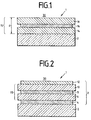
- the inventive doped diamond layer between two high-purity to embed undoped diamond layers, so that the low-e layer system as a whole three arranged one on top of the other on a substrate Layers.
- the individual diamond layers having individual layers to produce synthetically.
- a plasma chemical deposition process preferably a chemical vapor deposition process, i.e. CVD, proposed.
- CVD chemical vapor deposition process
- Diamond layers from the gas phase with the addition of atomic hydrogen deposited on a substrate This method can be used on substrates closed, polycrystalline to be deposited Synthesize diamond layers that according to the invention can be used as low-E layers.
- the layers 14 and 18 each consist of high-purity, preferably polycrystalline, in diamond structure crystallized carbon layers.
- the layers 14, 16, 18 are each by means of a CVD deposition process deposited on the substrate 2.
- the substrate 2 consists of a light-transparent Vitreous, e.g. a window glass.
- the low-E layer systems shown in FIG. 1 or FIG. 2 are e.g. as an electrically conductive Layer system for use with automotive windows usable, the conductive layers by means of Current flow can be heated as an ohmic resistor are and for deicing the car windows to serve. Furthermore, the layer systems shown are shielding as electromagnetic fields, light-transparent wall can be used.
- the low-E layer systems shown in FIGS. 1 and 2 15 and 3 are on the order Exterior surfaces of architectural glass provided, which e.g. in climates with abrasive on glass surfaces acting particles, e.g. Sand Wind currents to be used or which through intensive cleaning processes high chemical and / or exposed to physical loads are.
- architectural glass e.g. in climates with abrasive on glass surfaces acting particles, e.g. Sand Wind currents to be used or which through intensive cleaning processes high chemical and / or exposed to physical loads are.
Abstract
Description
Die Erfindung betrifft ein Schichtensystem, das einen hohen Transmissionsgrad im sichtbaren Spektralbereich und eine hohen Reflexionsgrad im Wärmestrahlungsspektralbereich aufweist.The invention relates to a layer system that a high degree of transmission in the visible spectral range and a high degree of reflection in the heat radiation spectral range having.
Gattungsgemäße Schichtsysteme werden im allgemeinen als "Low-E" (Low-Emissivity) bezeichnet. Derartige Schichtsysteme, welche z.B. auf Flachgläsern aufgebracht sind, dienen dazu, Licht im sichtbaren Spektralbereich durchzulassen, jedoch längerwellige Wärmestrahlung zu reflektieren. Bei Verwendung derartiger Flachgläser für Fensterverglasungen tragen diese somit vorteilhaft dazu bei, die Wärmeabstrahlung aus einem Raum durch verglaste Fensterflächen zu minimieren.Generic layer systems are generally referred to as "low-E" (low emissivity). Such Layer systems which e.g. on flat glasses are used to light in pass through the visible spectral range, however to reflect longer-wave heat radiation. At Use of such flat glasses for window glazing thus advantageously contribute to the heat radiation from a room through glazed Minimize window areas.
Herkömmliche Low-E-Schichtsysteme bestehen im
Prinzip aus der folgenden Schichtenfolge:
Substrat / Metalloxyd / Metall / Metalloxyd.Conventional low-E layer systems basically consist of the following layer sequence:
Substrate / metal oxide / metal / metal oxide.
Ein derartiges Low-E-Schichtsystem wird zum Beispiel in der DE 42 11 363 beschrieben. Die eigentliche Funktionsschicht stellt die Metallschicht dar, die aus Metallen mit sehr niedrigem Strahlungsemissions-Koeffizienten besteht. Üblicherweise besteht die Metallschicht aus Silber, Gold oder auch aus Kupfer bzw. Legierungen dieser Metalle. Die Metalloxydschichten dienen dem Zweck, als Antireflexschicht zu wirken und gleichzeitig die Metallschicht gegen mechanische und/oder chemische Umwelteinwirkungen zu schützen. Vorgesehen sind auch mehrlagige Schutzschichten, die das Beständigkeitsverhalten gegenüber Umwelteinflüssen gattungsgemäßer Low-E-Schichtensysteme erhöhen.Such a low-E layer system is, for example described in DE 42 11 363. The real one Functional layer represents the metal layer are made of metals with very low radiation emission coefficients consists. Usually the metal layer consists of silver, gold or also from copper or alloys of these metals. The metal oxide layers serve the purpose as an anti-reflective layer to act and at the same time the metal layer against mechanical and / or chemical Protect environmental impacts. Are provided also multi-layer protective layers that determine the resistance behavior generic in relation to environmental influences Increase low-E layer systems.
Auf Grund der zunehmenden hohen Anforderungen an die optischen und energetischen Parameter von Low-E-Schichtensysteme sowie deren geforderte Resistenz gegenüber Umwelteinwirkungen hat sich gezeigt, daß herkömmliche Schichtsysteme diesen Erfordernissen nicht mehr gerecht werden. Bekannt sind aus Indium-Zinn-Oxyd (ITO) bestehende, widerstandsfähige Schutzschichten, welche Emissivitätswerte zwischen 0,15 und 0,13 besitzen. Ein Nachteil der Verwendung derartiger ITO-Schichten aufweisender Low-E-Schichtensysteme ist, daß die großtechnische Herstellung, z.B. für Architekturglasanwendungen wegen des extrem hohen Materialpreises für Indium sehr teuer ist. Alternativ hierzu werden aus Zinnoxyd gefertigte Low-E-Schichten verwendet, die z.B. aus Kostengründen pyrolytisch auf dem Trägermaterial aufgebracht werden und einen Emissivitätswert von 0,4 besitzen.Due to the increasing high demands on the optical and energetic parameters of low-E layer systems as well as their required resistance against environmental effects has been shown that conventional layer systems meet these requirements no longer do it justice. Known are made of indium tin oxide (ITO), resistant Protective layers, what emissivity values have between 0.15 and 0.13. A disadvantage using such ITO layers Low-E layer systems is that industrial production, e.g. for architectural glass applications because of the extremely high material price is very expensive for indium. Alternatively For this purpose, low-E layers are made of tin oxide used, e.g. for cost reasons pyrolytically applied to the carrier material and have an emissivity value of 0.4.
Der Erfindung liegt die Aufgabe zu Grunde, ein Low-E-Schichtensystem der eingangs genannten Art zu schaffen, welches eine erhöhte Beständigkeit gegenüber chemischen und/oder mechanischen Einwirkungen aufweist und die Mängel der bekannten technischen Lösungen vermeidet.The invention is based on the object Low-E layer system of the type mentioned at the beginning to create which has increased durability against chemical and / or mechanical influences has and the shortcomings of the known technical Avoids solutions.
Erfindungsgemäß wird diese Aufgabe durch ein Low-E-Schichtensystem
gelöst, welches mindestens eine
mit Fremdatomen dotierte, in Diamantstruktur auskristallisierte
Kohlenstoffschicht aufweist, wobei
die Strahlungsemissivität im Wärmestrahlungsspektralbereich
und die elektrische Leitfähigkeit dieser
Diamantschicht in Abhängigkeit der Dotierungskonzentration
cA der Fremdatome in der Kohlenstoffschicht
einstellbar ist. Als Dotierungsmaterial
wird gemäß Anspruch 2 eine Bor-Dotierung vorgeschlagen,
wodurch die Diamantschicht p-Leitung
aufweist. Die Verwendung erfindungsgemäßer, dotierter
Diamantschichten für Low-E-Schichtensysteme
weist den entscheidenden Vorteil auf, daß
derartige Schichten eine geringe Emissivität im
infraroten Spektralbereich einerseits, eine hohe
Transparenz im visuellen Spektralbereich und darüber
hinaus die für derartige Schichtsysteme gewünschten
physikalischen und chemischen Eigenschaften,
nämlich eine große Härte, hohe Abriebfestigkeit
und damit eine chemische Beständigkeit
gegenüber jeglichen Umwelteinflüssen miteinander
vereinen. Durch die Erfindung wird insbesondere
vorteilhaft ein Schichtensystem bereitgestellt,
das vergleichbar niedrige Emissivitätswerte wie
herkömmliche, auf Silberbasis hergestellte Low-E-Schichtensysteme
aufweist, jedoch deren geringe
Beständigkeit gegenüber Umwelteinflüssen vermeidet.
Erfindungsgemäße Low-E-Schichtensysteme können
so z.B. vorteilhaft auf Außenflächen von Glasfenstern
eingesetzt werden. Durch diese neue Verwendungsmöglichkeit
von Low-E-Schichtensystemen,
nämlich auf Außenflächen von Glasfenstern, wird
auch eine deutliche Herabsetzung des sogenannten
U-Wertes erzielt. Unter dem U-Wert wird die thermische
Leitfähigkeit einer Grenzfläche verstanden,
die in SI-Einheiten die Einheit W/m2K besitzt, mit
W: Energie, m2: Fläche, K: Temperatur in K. Die
Fremdatomkonzentration in der Low-E-Diamantschicht
beträgt erfindungsgemäß zwischen 1020 Atome/cm3 und
1022 Atome/cm3 (siehe Anspruch 3). Mittels der
Fremdatomkonzentration ist, wie in Anspruch 9 angegeben,
die elektrische Leitfähigkeit der Diamantschicht
einstellbar, wobei vorgeschlagen wird,
den Flächenwiderstand der Diamantschicht zwischen
1 Ω/□ und 10 Ω/□ zu wählen.According to the invention, this object is achieved by a low-E layer system which has at least one carbon layer doped with foreign atoms and crystallized out in a diamond structure, the radiation emissivity in the heat radiation spectral range and the electrical conductivity of this diamond layer being adjustable as a function of the doping concentration c A of the foreign atoms in the carbon layer . Boron doping is proposed as doping material according to
Weiterhin wird vorgeschlagen, die erfindungsgemäße, dotierte Diamantschicht zwischen zwei hochreinen, nicht dotierten Diamantschichten einzubetten, so daß das Low-E-Schichtensystem insgesamt aus drei aufeinander auf einem Substrat angeordneten Schichten besteht. It is also proposed that the inventive doped diamond layer between two high-purity, to embed undoped diamond layers, so that the low-e layer system as a whole three arranged one on top of the other on a substrate Layers.
Zur optischen Anpassung der Diamantschichten an das Substrat einerseits und an das umgebende Medium andererseits ist jeweils eine unmittelbar auf dem Substrat bzw. auf der obersten Diamantschicht anliegende Schicht vorgesehen, welche aus einem Metalloxyd, vorzugsweise aus mindestens einer der Verbindungen Zinkoxyd, Titandioxyd, Aluminiumoxyd, Siliziumdioxyd oder Zinnoxyd, wie in Anspruch 5 bzw. 6 aufgeführt, hergestellt ist. Die Gesamtschichtdicke d eines erfindungsgemäßen, mindestens drei Diamantschichten aufweisenden Schichtensystems beträgt maximal 1,5 µm. Die als optische Anpassungsschichten vorgesehenen Metalloxydschichten weisen Schichtdicken zwischen 0,05 µm und 0,2 µm auf. Alternativ wird vorgeschlagen, die Anpassungsschichten und/oder die unmittelbar benachbart an der dotierten Diamantschicht anliegenden Schichten aus C-BN, i.e. kubisches Bornitrid, zu fertigen.For optical adjustment of the diamond layers the substrate on the one hand and the surrounding medium on the other hand, one is immediately open the substrate or on the top diamond layer adjacent layer provided, which consists of a Metal oxide, preferably from at least one of the Compounds zinc oxide, titanium dioxide, aluminum oxide, Silicon dioxide or tin oxide as in claim 5 or 6 listed, is produced. The total layer thickness d of an inventive, at least three layer system comprising diamond layers is a maximum of 1.5 µm. The as optical matching layers provided metal oxide layers have layer thicknesses between 0.05 µm and 0.2 µm on. Alternatively, it is proposed to use the adaptation layers and / or the immediately adjacent applied to the doped diamond layer C-BN layers, i.e. cubic boron nitride, too manufacture.
Vorgeschlagen wird, die einzelne Diamantschichten
aufweisenden Einzelschichten synthetisch herzustellen.
Zur Herstellung eines erfindungsgemäßen,
mindestens eine Diamantschicht als Low-E-Schicht
aufweisenden Schichtensystems wird wie in Anspruch
12 angegeben, ein plasmachemisches Abscheidungsverfahren,
vorzugsweise ein Chemical-Vapor-Deposition-Abscheidungsverfahren,
i.e. CVD, vorgeschlagen.
Bei derartigen Abscheideverfahren werden
Diamantschichten aus der Gasphase unter Zugabe von
atomarem Wasserstoff auf einem Substrat abgeschieden.
Mit diesem Verfahren lassen sich auf Substraten
abzuscheidende, geschlossene, polykristalline
Diamantschichten synthetisch herstellen, die erfindungsgemäß
als Low-E-Schichten verwendbar sind.It is suggested the individual diamond layers
having individual layers to produce synthetically.
To produce an inventive
at least one diamond layer as a low-E layer
having layer system is as in
Weitere vorteilhafte Eigenschaften bevorzugter Ausführungsformen des Erfindungsgegenstandes sind in den auf den Hauptanspruch zurückbezogenen Unteransprüchen angegeben.More advantageous properties more preferred Embodiments of the subject matter of the invention in the subclaims related to the main claim specified.
Nachfolgend werden zwei besonders vorteilhafte Low-E-Schichtsysteme gemäß der Erfindung dargestellt. Es zeigen:
Figur 1- ein drei Einzelschichten umfassendes Low-E-Schichtensystem, aufgebracht auf einem Substrat;
Figur 2- ein aus fünf Einzelschichten bestehendes Low-E-Schichtensystem auf einem Substrat.
- Figure 1
- a three-layer low-E layer system applied to a substrate;
- Figure 2
- a low-E layer system consisting of five individual layers on a substrate.
Das in Figur 1 dargestellte Low-E-Schichtsystem besteht aus insgesamt drei Einzelschichten, nämlich:
- einer ersten, auf einem
Substrat 2 aufliegenden Schicht 14, - einer zweiten, auf der Schicht 14 aufgebrachten, als Low-E-Schicht wirkenden, mit Fremdatomen dotierten Kohlenstoffschicht, welche in Diamantstruktur auskristallisiert ist und
- einer die
Schicht 16überdeckenden Schutzschicht 18.
- a first layer 14 resting on a
substrate 2, - a second carbon layer applied on the layer 14 and acting as a low-E layer and doped with foreign atoms, which is crystallized out in a diamond structure and
- a
protective layer 18 covering thelayer 16.
Die Schichten 14 und 18 bestehen aus jeweils hochreinen,
vorzugsweise polykristallinen, in Diamantstruktur
kristallisierten Kohlenstoffschichten.
Die Schichten 14,16,18 sind jeweils mittels eines
CVD-Abscheideverfahrens auf dem Substrat 2 abgeschieden.
Das Substrat 2 besteht aus einem lichttransparenten
Glaskörper, z.B. einem Fensterglas.The
Gemäß dem zweiten, in Figur 2 dargestellten Ausführungsbeispiel ist vorgesehen, das in Figur 1 dargestellte, die Diamantschichten 14,16,18 umfassende Schichtensystem 15 zwischen zwei als optische Anpassungsschichten wirkende Zwischenschichten 4,12 einzubetten. Das Low-E-Schichtensystem, wie in Figur 2 dargestellt, umfaßt insgesamt fünf Einzelschichten, nämlich:
- eine erste, auf dem
Substrat 2aufliegende Schicht 4, - eine zweite, aus Diamant bestehende Schicht 6,
- eine dritte, Diamantstruktur aufweisende,
mit Fremdatomen dotierte
Kohlenstoffschicht 8, - eine vierte, die
Kohlenstoffschicht 8 bedeckende,hochreine Diamantschicht 10 und - eine
fünfte Schicht 12, die das Schichtensystem gegenüber dem umgebenden Medium abgrenzt.
- a
first layer 4 lying on thesubstrate 2, - a second layer 6 consisting of diamond,
- a
third carbon layer 8 having a diamond structure and doped with foreign atoms, - a fourth, the
carbon layer 8 covering, high-purity diamond layer 10 and - a
fifth layer 12 which delimits the layer system from the surrounding medium.
Die als optische Anpassungsschichten vorgesehenen
Zwischenschichten 4 und 12 bestehen aus Metalloxydverbindungen,
z.B. aus TiO2, Al2O3, SiO2, SnO2
oder ZnO. Die Schichtdicken der Anpassungsschichten
4 und 12 betragen zwischen 0,05 µm und 0,2 µm.
Das aus den drei aufeinanderfolgenden Schichten
6,8,10 bzw. 14,16,18 bestehende Schichtensystem 15
weist insgesamt eine Schichtendicke von < 1,5 µm
auf.The
Die in Figur 1 bzw. Figur 2 dargestellten Low-E-Schichtsysteme sind z.B. als elektrisch leitfähiges Schichtensystem zum Einsatz bei Kfz-Scheiben verwendbar, wobei die leitfähigen Schichten mittels Stromdurchfluß als Ohmscher Widerstand erwärmbar sind und zur Enteisung der Kfz-Scheiben dienen. Weiterhin sind die dargestellten Schichtensysteme als elektromagnetische Felder abschirmende, lichttransparente Wand verwendbar.The low-E layer systems shown in FIG. 1 or FIG. 2 are e.g. as an electrically conductive Layer system for use with automotive windows usable, the conductive layers by means of Current flow can be heated as an ohmic resistor are and for deicing the car windows to serve. Furthermore, the layer systems shown are shielding as electromagnetic fields, light-transparent wall can be used.
Die in den Figuren 1 und 2 dargestellten Low-E-Schichtensysteme 15 bzw. 3 sind zum Auftrag auf Außenflächen von Architekturgläsern vorgesehen, welche z.B. in Klimazonen mit abrasiv auf Glasflächen einwirkenden Partikeln, wie z.B. Sand aufweisenden Windströmungen, einzusetzen sind oder welche durch intensive Reinigungsprozesse hohen chemischen und/oder physikalischen Belastungen ausgesetzt sind. The low-E layer systems shown in FIGS. 1 and 2 15 and 3 are on the order Exterior surfaces of architectural glass provided, which e.g. in climates with abrasive on glass surfaces acting particles, e.g. Sand Wind currents to be used or which through intensive cleaning processes high chemical and / or exposed to physical loads are.
- 11
- beschichtete Scheibecoated disc
- 22nd
- SubstratSubstrate
- 33rd
- SchichtensystemLayer system
- 44th
- erste Schichtfirst layer
- 66
- zweite Schichtsecond layer
- 88th
- dritte Schicht, dotierte Diamantschichtthird layer, doped diamond layer
- 1010th
- vierte Schichtfourth layer
- 1212th
- DeckschichtTop layer
- 1313
- beschichtete Scheibecoated disc
- 1414
- erste Schichtfirst layer
- 1616
- zweite Schicht, dotierte Diamantschichtsecond layer, doped diamond layer
- 1818th
- DeckschichtTop layer
- 3030th
- umgebendes Medium, Atmosphäresurrounding medium, atmosphere
- dd
- GesamtschichtdickeTotal layer thickness
Claims (12)
Applications Claiming Priority (2)
| Application Number | Priority Date | Filing Date | Title |
|---|---|---|---|
| DE19643550A DE19643550A1 (en) | 1996-10-24 | 1996-10-24 | Light-transparent, heat radiation reflecting layer system |
| DE19643550 | 1996-10-24 |
Publications (2)
| Publication Number | Publication Date |
|---|---|
| EP0838698A2 true EP0838698A2 (en) | 1998-04-29 |
| EP0838698A3 EP0838698A3 (en) | 1998-09-16 |
Family
ID=7809436
Family Applications (1)
| Application Number | Title | Priority Date | Filing Date |
|---|---|---|---|
| EP97112249A Ceased EP0838698A3 (en) | 1996-10-24 | 1997-07-17 | Thermally reflecting laminate, transparent to visible light |
Country Status (6)
| Country | Link |
|---|---|
| US (1) | US5976683A (en) |
| EP (1) | EP0838698A3 (en) |
| JP (1) | JPH10133014A (en) |
| KR (1) | KR19980032328A (en) |
| DE (1) | DE19643550A1 (en) |
| TW (1) | TW493084B (en) |
Cited By (3)
| Publication number | Priority date | Publication date | Assignee | Title |
|---|---|---|---|---|
| WO2002036513A2 (en) * | 2000-10-30 | 2002-05-10 | Guardian Industries Corp. | Low-e coating system including protective dlc |
| WO2002038515A3 (en) * | 2000-10-30 | 2002-07-04 | Guardian Industries | Solar management coating system including protective dlc |
| EP1338576A1 (en) * | 1999-05-03 | 2003-08-27 | Guardian Industries Corp. | Highly tetrahedral amorphous carbon coating on glass |
Families Citing this family (39)
| Publication number | Priority date | Publication date | Assignee | Title |
|---|---|---|---|---|
| WO2002046490A2 (en) * | 2000-12-06 | 2002-06-13 | Fraunhofer Gesellschaft zur Förderung der angewandten Forschung e.V. | Coated substrate having a low emissivity |
| US6783253B2 (en) | 2002-03-21 | 2004-08-31 | Guardian Industries Corp. | First surface mirror with DLC coating |
| US6934085B2 (en) * | 2003-10-21 | 2005-08-23 | Guardian Industries Corp. | First surface mirror with chromium inclusive nucleation layer |
| US7521292B2 (en) | 2004-06-04 | 2009-04-21 | The Board Of Trustees Of The University Of Illinois | Stretchable form of single crystal silicon for high performance electronics on rubber substrates |
| EP2650906A3 (en) | 2004-06-04 | 2015-02-18 | The Board of Trustees of the University of Illinois | Methods and devices for fabricating and assembling printable semiconductor elements |
| US7799699B2 (en) | 2004-06-04 | 2010-09-21 | The Board Of Trustees Of The University Of Illinois | Printable semiconductor structures and related methods of making and assembling |
| US7678459B2 (en) * | 2004-09-21 | 2010-03-16 | Guardian Industries Corp. | First surface mirror with silicon-metal oxide nucleation layer |
| US7276289B2 (en) * | 2004-09-21 | 2007-10-02 | Guardian Industries Corp. | First surface mirror with metal oxide nucleation layer |
| US8142035B2 (en) * | 2005-08-18 | 2012-03-27 | Guardian Industries Corp. | Mirror with selectively oxidized areas for memory effect and method of making same |
| US7771103B2 (en) * | 2005-09-20 | 2010-08-10 | Guardian Industries Corp. | Optical diffuser with IR and/or UV blocking coating |
| US20080073203A1 (en) * | 2006-09-19 | 2008-03-27 | Guardian Industries Corp. | Method of making first surface mirror with oxide graded reflecting layer structure |
| KR101610885B1 (en) | 2007-01-17 | 2016-04-08 | 더 보오드 오브 트러스티스 오브 더 유니버시티 오브 일리노이즈 | Optical systems fabricated by printing-based assembly |
| US9297061B2 (en) * | 2007-02-16 | 2016-03-29 | Kaneka Corporation | Transparent electroconductive film and process for producing the same |
| JP5743553B2 (en) | 2008-03-05 | 2015-07-01 | ザ ボード オブ トラスティーズ オブ ザ ユニヴァーシティー オブ イリノイ | Stretchable and foldable electronic devices |
| US8470701B2 (en) | 2008-04-03 | 2013-06-25 | Advanced Diamond Technologies, Inc. | Printable, flexible and stretchable diamond for thermal management |
| US8097926B2 (en) | 2008-10-07 | 2012-01-17 | Mc10, Inc. | Systems, methods, and devices having stretchable integrated circuitry for sensing and delivering therapy |
| US8389862B2 (en) | 2008-10-07 | 2013-03-05 | Mc10, Inc. | Extremely stretchable electronics |
| US8886334B2 (en) | 2008-10-07 | 2014-11-11 | Mc10, Inc. | Systems, methods, and devices using stretchable or flexible electronics for medical applications |
| US8372726B2 (en) | 2008-10-07 | 2013-02-12 | Mc10, Inc. | Methods and applications of non-planar imaging arrays |
| EP2349440B1 (en) | 2008-10-07 | 2019-08-21 | Mc10, Inc. | Catheter balloon having stretchable integrated circuitry and sensor array |
| TWI592996B (en) | 2009-05-12 | 2017-07-21 | 美國伊利諾大學理事會 | Printed assemblies of ultrathin, microscale inorganic light emitting diodes for deformable and semitransparent displays |
| WO2011041727A1 (en) | 2009-10-01 | 2011-04-07 | Mc10, Inc. | Protective cases with integrated electronics |
| WO2011084450A1 (en) | 2009-12-16 | 2011-07-14 | The Board Of Trustees Of The University Of Illinois | Electrophysiology in-vivo using conformal electronics |
| US10441185B2 (en) | 2009-12-16 | 2019-10-15 | The Board Of Trustees Of The University Of Illinois | Flexible and stretchable electronic systems for epidermal electronics |
| US9936574B2 (en) | 2009-12-16 | 2018-04-03 | The Board Of Trustees Of The University Of Illinois | Waterproof stretchable optoelectronics |
| KR101724273B1 (en) | 2010-03-17 | 2017-04-07 | 더 보드 오브 트러스티즈 오브 더 유니버시티 오브 일리노이 | implantable biomedical devices on bioresorbable substrates |
| US9442285B2 (en) | 2011-01-14 | 2016-09-13 | The Board Of Trustees Of The University Of Illinois | Optical component array having adjustable curvature |
| WO2012158709A1 (en) | 2011-05-16 | 2012-11-22 | The Board Of Trustees Of The University Of Illinois | Thermally managed led arrays assembled by printing |
| JP2014523633A (en) | 2011-05-27 | 2014-09-11 | エムシー10 インコーポレイテッド | Electronic, optical and / or mechanical devices and systems and methods of manufacturing these devices and systems |
| US8934965B2 (en) | 2011-06-03 | 2015-01-13 | The Board Of Trustees Of The University Of Illinois | Conformable actively multiplexed high-density surface electrode array for brain interfacing |
| EP2786644B1 (en) | 2011-12-01 | 2019-04-10 | The Board of Trustees of the University of Illionis | Transient devices designed to undergo programmable transformations |
| JP2015521303A (en) | 2012-03-30 | 2015-07-27 | ザ ボード オブ トラスティーズ オブ ザ ユニヴァーシ | An electronic device that can be attached to the surface and can be attached to an accessory |
| US9171794B2 (en) | 2012-10-09 | 2015-10-27 | Mc10, Inc. | Embedding thin chips in polymer |
| CN103407220B (en) * | 2013-05-08 | 2015-12-02 | 上海浩驰科技股份有限公司 | Be provided with the film of carbon crystal layer |
| US10695872B2 (en) * | 2015-03-11 | 2020-06-30 | Lockheed Martin Corporation | Heat spreaders fabricated from metal nanoparticles |
| US20160338494A1 (en) * | 2015-05-20 | 2016-11-24 | Gregory J. Beinecke | Seatback Utility Device and Concession Holder |
| EP3304130B1 (en) | 2015-06-01 | 2021-10-06 | The Board of Trustees of the University of Illinois | Alternative approach to uv sensing |
| CN107851208B (en) | 2015-06-01 | 2021-09-10 | 伊利诺伊大学评议会 | Miniaturized electronic system with wireless power supply and near field communication capability |
| US10925543B2 (en) | 2015-11-11 | 2021-02-23 | The Board Of Trustees Of The University Of Illinois | Bioresorbable silicon electronics for transient implants |
Citations (4)
| Publication number | Priority date | Publication date | Assignee | Title |
|---|---|---|---|---|
| EP0564709A1 (en) * | 1991-12-13 | 1993-10-13 | Balzers Aktiengesellschaft | Coated transparent substrate, use thereof, method and apparatus of manufacturing such coatings, and hafnium-oxynitride HfOxNy with 1.5 x/y 3 and 2.6 n 2.8 |
| EP0567735A1 (en) * | 1992-04-30 | 1993-11-03 | Guardian Industries Corp. | High performance, durable, low-E glass and method of making same |
| WO1994003331A1 (en) * | 1992-08-03 | 1994-02-17 | Diamonex, Incorporated | Abrasion wear resistant coated substrate product |
| EP0658066A2 (en) * | 1993-12-09 | 1995-06-14 | Sumitomo Electric Industries, Limited | Diamond heater |
Family Cites Families (17)
| Publication number | Priority date | Publication date | Assignee | Title |
|---|---|---|---|---|
| DE3039821A1 (en) * | 1980-10-22 | 1982-06-03 | Robert Bosch Gmbh, 7000 Stuttgart | MULTI-LAYER SYSTEM FOR HEAT PROTECTION APPLICATION |
| ATE12760T1 (en) * | 1981-10-09 | 1985-05-15 | Bosch Gmbh Robert | ENVIRONMENT RESISTANT MULTI-LAYER SYSTEM FOR THERMAL PROTECTION APPLICATION. |
| DE3140100C2 (en) * | 1981-10-09 | 1986-11-27 | Robert Bosch Gmbh, 7000 Stuttgart | Multi-layer system for heat protection application |
| US5138808A (en) * | 1986-10-14 | 1992-08-18 | Superlite Block | Masonry block wall system and method |
| US4939043A (en) * | 1987-02-13 | 1990-07-03 | Northrop Corporation | Optically transparent electrically conductive semiconductor windows |
| KR900008505B1 (en) * | 1987-02-24 | 1990-11-24 | 세미콘덕터 에너지 라보라터리 캄파니 리미티드 | Microwave enhanced cvd method for depositing carbon |
| ZA888034B (en) * | 1987-12-17 | 1989-06-28 | Gen Electric | Diamond growth process |
| DE3807600C2 (en) * | 1988-03-08 | 1999-06-17 | Interpane Entw & Beratungsges | Low-reflecting, highly transparent sun protection and / or heat-insulating covering for a substrate made of transparent material, process for producing the covering and uses of the covering, which has a neutral effect in both the external and external view |
| JPH02217397A (en) * | 1989-02-15 | 1990-08-30 | Kobe Steel Ltd | Vapor-phase synthesis of thin film of n-type semiconductor diamond |
| DE4020696A1 (en) * | 1990-06-29 | 1992-01-09 | Renker Gmbh & Co Kg Zweigniede | MULTI-LAYER SYSTEM WITH A HIGH REFLECTION CAPACITY IN THE INFRARED SPECTRAL AREA AND WITH A HIGH TRANSMISSION CAPACITY IN THE VISIBLE AREA |
| US5254862A (en) * | 1991-08-14 | 1993-10-19 | Kobe Steel U.S.A., Inc. | Diamond field-effect transistor with a particular boron distribution profile |
| DE4211363A1 (en) * | 1992-04-04 | 1993-10-07 | Leybold Ag | Coating transparent substrate by cathode sputtering - to produce disks of high transmission behaviour in the visible region and giving high reflection to heat radiation |
| JPH05299705A (en) * | 1992-04-16 | 1993-11-12 | Kobe Steel Ltd | Diamond thin film electronic device and manufacture thereof |
| US5362975A (en) * | 1992-09-02 | 1994-11-08 | Kobe Steel Usa | Diamond-based chemical sensors |
| US5371383A (en) * | 1993-05-14 | 1994-12-06 | Kobe Steel Usa Inc. | Highly oriented diamond film field-effect transistor |
| JP3563093B2 (en) * | 1993-09-24 | 2004-09-08 | 住友電気工業株式会社 | Semiconductor device |
| FR2727322B1 (en) * | 1994-11-30 | 1996-12-27 | Kodak Pathe | METHOD FOR SUBLIMATING A SOLID MATERIAL AND DEVICE FOR CARRYING OUT THE METHOD |
-
1996
- 1996-10-24 DE DE19643550A patent/DE19643550A1/en not_active Withdrawn
-
1997
- 1997-07-17 EP EP97112249A patent/EP0838698A3/en not_active Ceased
- 1997-07-28 TW TW086110717A patent/TW493084B/en active
- 1997-08-29 KR KR1019970042523A patent/KR19980032328A/en active IP Right Grant
- 1997-10-22 JP JP9289857A patent/JPH10133014A/en active Pending
- 1997-10-22 US US08/955,964 patent/US5976683A/en not_active Expired - Fee Related
Patent Citations (4)
| Publication number | Priority date | Publication date | Assignee | Title |
|---|---|---|---|---|
| EP0564709A1 (en) * | 1991-12-13 | 1993-10-13 | Balzers Aktiengesellschaft | Coated transparent substrate, use thereof, method and apparatus of manufacturing such coatings, and hafnium-oxynitride HfOxNy with 1.5 x/y 3 and 2.6 n 2.8 |
| EP0567735A1 (en) * | 1992-04-30 | 1993-11-03 | Guardian Industries Corp. | High performance, durable, low-E glass and method of making same |
| WO1994003331A1 (en) * | 1992-08-03 | 1994-02-17 | Diamonex, Incorporated | Abrasion wear resistant coated substrate product |
| EP0658066A2 (en) * | 1993-12-09 | 1995-06-14 | Sumitomo Electric Industries, Limited | Diamond heater |
Non-Patent Citations (1)
| Title |
|---|
| LETTINGTON A H: "OPTICAL PROPERTIES AND APPLICATIONS OF DIAMOND AND DIAMOND-LIKE CARBON THIN FILMS" HARD MATERIALS IN OPTICS, THE HAGUE, MARCH 14 - 15, 1990, Nr. VOL. 1275, 14.M{rz 1990, RIBBING C G (ED ), Seiten 14-24, XP000215979 * |
Cited By (6)
| Publication number | Priority date | Publication date | Assignee | Title |
|---|---|---|---|---|
| EP1338576A1 (en) * | 1999-05-03 | 2003-08-27 | Guardian Industries Corp. | Highly tetrahedral amorphous carbon coating on glass |
| US6713178B2 (en) | 1999-05-03 | 2004-03-30 | Vijayen S. Veerasamy | Highly tetrahedral amorphous carbon coating on glass |
| US7858150B2 (en) | 1999-05-03 | 2010-12-28 | Guardian Industries Corp. | Method of making heat treatable coated article with protective layer |
| WO2002036513A2 (en) * | 2000-10-30 | 2002-05-10 | Guardian Industries Corp. | Low-e coating system including protective dlc |
| WO2002038515A3 (en) * | 2000-10-30 | 2002-07-04 | Guardian Industries | Solar management coating system including protective dlc |
| WO2002036513A3 (en) * | 2000-10-30 | 2002-07-04 | Guardian Industries | Low-e coating system including protective dlc |
Also Published As
| Publication number | Publication date |
|---|---|
| US5976683A (en) | 1999-11-02 |
| KR19980032328A (en) | 1998-07-25 |
| EP0838698A3 (en) | 1998-09-16 |
| TW493084B (en) | 2002-07-01 |
| JPH10133014A (en) | 1998-05-22 |
| DE19643550A1 (en) | 1998-05-14 |
Similar Documents
| Publication | Publication Date | Title |
|---|---|---|
| EP0838698A2 (en) | Thermally reflecting laminate, transparent to visible light | |
| EP3720701B1 (en) | Laminated glass pane with solar control coating and thermal radiation reflective coating | |
| EP2958872B1 (en) | Pane with coating that reflects thermal radiation | |
| DE102014104799B4 (en) | Substrate with a coating to increase scratch resistance, process for its production and its use | |
| DE69531281T2 (en) | Glass substrates coated with a thin layer structure with reflective properties for infrared and / or solar radiation | |
| DE60305730T2 (en) | INFRARED REFLECTIVE HISTORICAL STRUCTURE | |
| DE69919904T2 (en) | GLAZED WINDOW | |
| DE69920278T2 (en) | GLAZED WINDOW | |
| EP2007694B1 (en) | Weather-resistant layer system | |
| DE10105199C1 (en) | Thermally loaded low emissivity layer system used for glass window panes in buildings and vehicles comprises silver functional layer, metal nitride layer, sacrificial metal layer, dielectric base layer and reflection-reducing covering layer | |
| EP3613257A1 (en) | Pane having heatable tco coating | |
| WO2018206236A1 (en) | Pane having an electrically conductive coating, with reduced visibility of fingerprints | |
| DE102017102377A1 (en) | Coated protective glazing | |
| DE102014002965A1 (en) | Layer system of a transparent substrate and method for producing a layer system | |
| DE69833099T2 (en) | Transparent substrates with an accumulation of layers with infrared and / or solar radiation reflecting properties | |
| DE102011114669B3 (en) | Coating system for solar control glass, solar control glass and process for the production of solar control glass | |
| WO2003104519A1 (en) | Method and device for coating a substrate with a layer system (zno+ag) and coated substrate | |
| EP0834483B1 (en) | Thermally insulating coating system for transparent substrates | |
| EP1529761B1 (en) | Thermally highly stable low-E coating system, its fabrication process and use of a substrate coated with such a coating system | |
| DE102011105718B4 (en) | Semitransparent layer system with high IR reflection, process for its production and architectural glass element | |
| DE202019104357U1 (en) | Improved Resistance of PDLC Films to Radiation from IR and UV Reflective Coatings on Page II of a Composite Disc | |
| EP1754690B1 (en) | Glazing unit and method for its production | |
| DE10042194A1 (en) | Multilayer heat-reflective coating system for transparent substrates, especially float glass, has a gradient of at least two materials in at least one of the layers | |
| DE10131932C2 (en) | Process for producing a heat-reflecting layer system for transparent substrates and layer system produced thereafter | |
| DE202020105642U1 (en) | compound pane |
Legal Events
| Date | Code | Title | Description |
|---|---|---|---|
| PUAI | Public reference made under article 153(3) epc to a published international application that has entered the european phase |
Free format text: ORIGINAL CODE: 0009012 |
|
| AK | Designated contracting states |
Kind code of ref document: A2 Designated state(s): BE CH DE ES FR GB IT LI LU NL SE |
|
| PUAL | Search report despatched |
Free format text: ORIGINAL CODE: 0009013 |
|
| AK | Designated contracting states |
Kind code of ref document: A3 Designated state(s): AT BE CH DE DK ES FI FR GB GR IE IT LI LU MC NL PT SE |
|
| 17P | Request for examination filed |
Effective date: 19981012 |
|
| AKX | Designation fees paid |
Free format text: BE CH DE ES FR GB IT LI LU NL SE |
|
| RBV | Designated contracting states (corrected) |
Designated state(s): BE CH DE ES FR GB IT LI LU NL SE |
|
| GRAG | Despatch of communication of intention to grant |
Free format text: ORIGINAL CODE: EPIDOS AGRA |
|
| 17Q | First examination report despatched |
Effective date: 20020618 |
|
| STAA | Information on the status of an ep patent application or granted ep patent |
Free format text: STATUS: THE APPLICATION HAS BEEN REFUSED |
|
| 18R | Application refused |
Effective date: 20021220 |