The present invention relates to a system and method for performing
reliability screening on semi-conductor wafers and particularly to a highly planar
burn in apparatus and method for uses including wafer level burn-in (WLBI),
diced die burn-in (DDBI), and packaged die burn-in (PDBI). More specifically,
the present invention relates to a burn-in system that includes a burn-in
substrate with a planar base, a temporary Z-axis connecting member, and a Z-axis
wafer level contact sheet electrically coupled to one another for screening
wafers, diced die, and packaged electronic components, their assembly and
use.
Semiconductor manufacturers who make integrated circuit chips begin
by manufacturing semiconductor wafers. Each wafer is typically 100 mm, 125
mm, 150 mm, 200 mm or 300 mm in diameter and contains anywhere from one
to several thousand chips or die on the wafer. When manufacture of the wafer
is completed, chips or die are cut or "diced" from the wafer and may later be
mounted into single chip or multiple chip packages for implementation in a
printed circuit board or other applications.
When manufacture of a wafer is completed, it is customary practice to
test each chip on the wafer to determine whether each chip, as manufactured,
electrically matches design criteria, matches performance criteria of the system
in which the chip is to be implemented, and will be reliable in operation. If a
chip fails electrical testing or reliability testing, the chip is not suitable for
implementation in a system without repairing the chip or exercising redundancy
features which may have been designed into the chip. Performance testing of
chips may be used to speed sort chips into different categories suitable for
different applications and sale at different prices.
Reliability testing is used to screen out chips having an undesirable
short life span. Typically, a significant percentage of a group of chips will fail
early in their lifetime due to marginal conditions during manufacture.
Subsequently, a very low percentage of the group will fail during an extended
period of use of the chips. Reliability screening of semiconductor chips is
typically performed by a process of supplying test signal patterns to chips under
test to repeatedly stimulate all devices and wires on a chip, and is typically
performed at elevated temperatures to simulate the first six months of
operation. Therefore, the screening procedure is known as burn-in.
Burning in chips tends to induce accelerated failures. Two examples of
such failures are contamination induced failure at via interfaces, and gates and
junctions, and in metal wires malformed during manufacture which may neck
down to very thin regions on the order of 50% of the design width, which varies
by technology and time but, is presently 0.35 µm. The metal in these necked
down regions will tend to drift in the direction of electrical current flow by a
mechanism known as electromigration, where the rate of drift is directly
proportional to current density, accelerated by elevated temperature. Upon
sufficient electromigration, an open circuit condition will occur in the necked
down region of the metal and cause a logical failure of the chip for some test
signal patterns. Gate oxide regions where transistors are formed using FET
transistor technology are also a frequent source of reliability failure. The
thickness of a gate oxide region of a transistor must be controlled within
exacting tolerances. If the gate oxide region of one or more transistors on a
chip, as manufactured, is too thin, the gate oxide may break down due to high
electric fields within the transistor when test patterns are applied to the chip.
Upon failure, output from the test patterns will evidence a failure.
While very valuable, the process of burn-in has historically been time
consuming and expensive for semiconductor manufacturers. Existing burn-in is
typically performed on integrated circuits at temperatures between 90°C to
125°C, for anywhere between 24 to 168 hours. Obviously, this slow rate of
reliability testing impedes volume production of functional semiconductors and
adds tremendous cost.
Many manufacturers have attempted to address low throughput of
known burn-in processes by creating burn-in boards onto which many diced
chips are placed in chip packages, and then the packages go into sockets on
the burn-in boards Thereafter, each chip on the test board is simultaneously
exercised with test patterns at elevated temperatures. Thus, many chips are
burned-in at once These systems effectively reduce the time required to burn-in
a large volume of chips. However, the added cost of packaging defective or
unreliable die is a significant shortcoming of such known burn-in processes.
Bare die burn-in (BDBI) is required to provide Known Good Die (KGD)
determinations for multi-chip module's (MCM's) and other bare die applications,
such as, chip-on-board (COB). Without bare die burn-in, yield of MCM's (and
other bare die applications) is severely impaired, resulting in higher product
costs. Current BDBI is typified by the Texas Instrument's "Die Mate"® product
where a bare die is placed into a temporary package and the burn-in test is
performed. The required alignment and handling steps in this procedure add
cost, process complexity, and time to provide bare dies that will be reliable or
"Known Good."
Another technique for improving throughput of the burn-in process is to
perform burn-in on whole or parts of whole wafers containing undiced
integrated circuits or chips. This process is known as wafer level burn-in
(WLBI). In wafer level burn-in, electrical terminals from a test apparatus are
brought into intimate contact with contact pads of one or more chips. It is
therefore less destructive than soldering chips to a burn-in board. However,
problems of planarity of electrical terminals of the test apparatus and with
mismatch between the coefficient of thermal expansion of the test apparatus
and the wafer under test exist.
These problems have been addressed to date by several different
techniques. For example, the industry uses a material known as CIC which is a
high pressure, high temperature, lamination of copper on the outside of an
interior INVAR sheet. One of the drawbacks with this material is that the
maximum thickness it can obtain is in sheets that are 62 mils thick. A second
drawback is that when CIC is manufactured, it is rolled on a big spool. As a
result, material from the outside of the spool to the inside of the spool has a
different plastic deformation and hence radius of curvature
Another drawback with the rolled CIC is that in order to get the desired
thickness and planarity, four pieces of CIC must be laminated together. There
must be an even number of CIC layers because two layers may be curved
down and one may be curved up. This results in an over balance in one
direction or the other. So the number of CIC sheets must be an evennumber --
2. 4 or 6. The drawback of using so many sheets of CIC is that since CIC is
very dense, the thicker the base, the heavier it becomes.
Another disadvantage of the CIC system is that, as manufactured, there
is an individual piece of copper on both sides of the INVAR 36 going through a
lamination process through rollers. The thickness of the copper top to bottom
changes. As a result of the different thicknesses, stress differential warpage
from top to bottom occurs, which is very detrimental during thermal excursions.
The thickness of the CIC could change as you go through the process also.
You cannot machine down the CIC to a uniform thickness because you may
machine off more on one side than the other.
Another disadvantage of the CIC system is that the material having the
highest coefficient of thermal expansion (CTE), the copper, is on the outside.
Thus, greater stress is generated with CIC.
One technique that is used to contact a wafer employs electrical
terminals, such as S shaped probes or Pogo® pins. With S shaped bendable
wire probes, the test apparatus is brought into proximity of the wafer, and the S
shaped probes are compressed back toward the test apparatus. The height of
the test apparatus over the wafer can then be varied to ensure contact between
each of the S shaped probes and contact pads on chips of the wafer, despite a
lack of planarity of the test apparatus and/or the wafer. However, the S shaped
probes are difficult to align to the contact pads of the chips on the wafer
because they vary in X, Y displacement, as well as, in the Z direction on
compression. Also, the number of pins used can be on the order of 20,000 to
40,000, or more, depending on the number of die per wafer and contacts per
die, thereby increasing the likelihood of non-alignment and mismatched pins.
Pogo® pins suffer from shortcomings similar to the S-shaped probes.
Although Pogo® pins are compressible, therefore compensating for some
planarity differences between the burn-in substrate and the wafer under test,
Pogo® pins present alignment challenges because the Pogo® pins must be put
into a fixture to hold them in place. The mechanical tooling can have holes in
slightly different locations due to normal tolerances.
Another technique for wafer level burn-in is described in U.S. Patent No.
5,541,524 to Tuckerman et al. There is disclosed a process of creating a burn-in
substrate having metallic contact pads that are ccined. Subsequently, solder
is formed on the top of the coins. The solder tops are then brought into contact
with the chip pads during burn-in testing. Here, the solder tops may not be
substantially planar, and must deform upon contact with the chip pads. Thus,
in order to achieve contact between all of the solder tops and the chip pads,
compressive forces must be applied which may damage some portion of the
chip pads. Furthermore, the solder tops must be periodically reworked by
melting them back to a hemisphere to ensure integrity of burn-in. However,
this can only be used to test wafers smaller than the apparatus. Currently, the
system can only test 150 mm wafers if the apparatus is manufactured on a 200
mm wafer, which does not provide a solution for testing 200 mm wafers.
Another technique for wafer level burn-in is described in U.S. Patent No.
4,968,931 to Littlebury et al. There, a flexible membrane probe, having a
plurality of contact pads, is compressed against a wafer having integrated
circuits with mating chip pads. An inflatable bladder is positioned behind the
flexible member probe to bring the probe contact pads into contact with the chip
contact pads. However, the bladder can only compensate for gross
irregularities in planarity. As the bladder inflates, the membrane is stretched
moving the contact points. Thus, alignment is difficult. Also, only a limited
number of traces can be implemented to bring signals from the wafer to the test
electronics, limiting the complexity of the system severely. In addition, the
system has a high coefficient of thermal expansion, resulting in positional
variation during thermal aging.
Thus. there exists a need to provide a wafer level burn-in device which
is highly planar and which is compliant, but at the same time maintains the
structural integrity of the contacts of the device for contacting chip pads on a
wafer. There is also a need for a burn-in system that eliminates the need for
solder reflow or cleaning. There is also a need to provide a burn-in device
having contacts, such as bumps, which are uniformly configured, precisely
disposed, with a high degree of structural integrity for coupling the contacts of a
wafer or the board under test. There further exists a need to provide a burn-in
device with a base that has a low coefficient of thermal expansion matched to
the wafer under test capable of successfully burning in large diameter wafers at
elevated temperatures of up to 150°C, and as high as 200°C.
The present invention relates to a system and method for performing
reliability screening on semi-conductor wafers that uses a highly planar burn-in
apparatus. The burn-in apparatus includes a burn-in substrate unit with a high
planarity base; a compliant, reusable, Z-axis member unit which can optionally
include an elastomer: and a reusable Z-axis laminated wafer level contact
sheet unit.
The burn-in substrate and wafer level contact sheet are electrically
coupled to one another through the irregularly shaped conductive Z-axis
pathways that extend through the thickness of the compliant, Z-axis member
that is sandwiched therebetween. The Z-axis pathways are electrically isolated
from one another in the X and Y axes directions.
A test signal from the burn-in substrate is conveyed to the component
being screened through bumps on the lower surface of the wafer level contact
sheet that are registered and in contact with the component being screened.
Each bump at its upper end has a 4 to 8 mil pad and terminates in a tip that
has a substantially planar configuration, and a surface diameter on the order of
0.25 mils and 2 mil (about 8 µm to 50 µm), and preferably 0.5 mils to 2 mil
(about 12 µm to 50 µm). Thus, the pad dimension to tip dimension ratio is
between 2:1 to 32:1, preferably between 4:1 to 32:1.
The laminated wafer level contact sheet unit has an upper and lower
surface and includes a plurality of uniformly configured conductive bumps on its
lower surface alignable with and corresponding to contact pads of an integrated
circuit or other electronic component. The geometric configuration of the bump
tip is sufficient to pierce an oxide layer that is formed on the contact pad of the
semiconductor component. The laminated contact sheet further includes a
plurality of contact pads on its upper surface, each individually electrically
connected to a corresponding conductive bump through an open cell, porous
layer having selective Z-axis conductivity.
The base unit has balancing layers disposed on an upper portion
thereof and circuitry layer on a lower portion thereof. The base unit includes a
degree of planarity that is less than 0.01 inches per linear foot, preferably 0.001
inches per linear foot. The balancing layer may include "dummy" layers to offset
and balance the circuitry layers. A plurality of first and second terminals
form part of the circuitry layer, with the first terminals being coupled to a
compliant, selectively conductive, Z-axis member, which may optionally contain
an elastomer. The second terminals are connectable to a test signal generator
and the first terminals.
The selectively Z-axis conductive compliant member is positioned
between the lower surface of the base unit and the upper surface of the wafer
level laminated contact sheet unit. The selectively conductive member
comprises a planar, open cell, porous material having an X, Y and Z axis, with
vertically defined cross-sectional areas electrically isolated in the X and Y axis
directions. The cross-sectional areas extend from one side of the material to
another side and are covered with conductive metal, thereby being capable of
electrically coupling the first terminals to corresponding contact pads on the
laminated wafer level contact sheet unit.
The selectively conductive member of the present invention may
contain an elastomer in the porous material. When an elastomer is used in
combination with the porous substrate, the temporary member is more
reusable and less compliant than a Z-axis member lacking an elastomer.
Generally, the burn-in screening of electronic components includes
positioning a burn-in unit in a temperature controlled environment, so that
downwardly depending conductive bumps can be coupled to corresponding
conductive pads of an electronic component to be screened. When the test
signal is generated, it is conveyed through the burn-in unit to the conductive
pads of the electronic component. The screening is usually conducted at a
temperature of at least 90°C, preferably between 125°C and 200°C, for 8 to
168 hours, preferably between 8 and 24 hours. The time of screening depends
on th burn-in temperature, lower temperatures, longer burn-in time. Test
signals are conveyed from said the terminal to the first terminals, a first set of
Z-axis condcutive pathways, a second set of Z-axis conductive pathways
through conductive bumps.
More specifically, the present invention provides a system for burn-in
screening of electronic components, such as an integrated circuit or a
semiconductor wafer, for example, where the wafer is contacted with a burn-in
unit having a base member with a planarity of less than 0.01 inches per linear
foot and a coefficient of thermal expansion that matches the coefficient of
thermal expansion of the wafer, +/- 3 ppm. The generated test signal is
conveyed through the burn-in unit to conductive pads on a wafer.
The present invention also relates to a burn-in screening procedure
where conductive bumps of a high planarity burn-in system are coupled to
conductive pads of an electronic component. The bumps have tips between
about 10 µm to 50 µm in diameter
Embodiments of the present invention will now be described, by
way of example, with reference to the accompanying drawings in
which:-
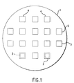
FIG. 1 depicts a wafer having a plurality of integrated circuit chips
formed thereon, each chip including a pattern of contact pads for electrical
connection to the chip.
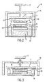
FIG. 2 depicts a burn-in device for wafer level burn-in with the
conductive bumps of the laminated contact sheet raised prior to contacting the
wafer.
FIG. 3 depicts the burn-in device of FIG. 2 with the conductive bumps of
the laminated contact sheet in intimate contact with the contact pads of the
wafer.
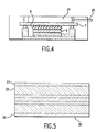
FIG. 4 depicts an alternate embodiment of a burn-in device, in which
intimate contact between the laminated contact sheet and the wafer under test
is controlled by an inflatable bladder.
FIG. 5 depicts the base unit with upper balancing "dummy" layers and
lower good "circuitry" layers according to the present invention.
FIG. 6 depicts a base unit having signal layers, a low CTE base layer,
and five balancing layers.
FIG. 7 depicts a cross-sectional view of the pad layer showing contact
pads and via holes through a dielectric layer.
FIG. 8 depicts a view of a signal layer illustrating signal traces on a
dielectric layer
FIG. 9 depicts a cross-sectional view through the low CTE base layer
illustrating its component layers.
FIGS. 10-12 schematically show the formation of irregular Z-axis
pathways extending through an open cell, porous substrate.
FIG. 13 depicts a porous substrate having isolated, Z-axis conductive
pathways extending through the thickness of the substrate and terminating in
conductive surface contacts.
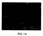
FIGS. 14 is a scanning electron micrograph of ePTFE material that is
used to prepare a Z-axis material which has a density of 0.22 gm/cm3, a
thickness of 76 µm and an air void volume of 70%.
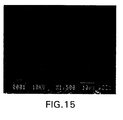
FIG. 15 is a scanning electron micrograph of an ePTFE material that is
used to prepare a Z-axis material which has a density of 0.40 gm/cm3, a
thickness of 40 µm and a 20% air void volume.
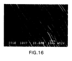
FIG. 16 is a scanning electron micrograph of an ePTFE material that is
used to prepare a Z-axis material which has a density of 0.35 gm/cm3, a of
thickness 100 µm and a 70% air void volume.
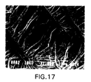
FIG. 17 is a scanning electron micrograph of an ePTFE material that is
used to prepare a Z-axis material which has a density of 0.20 gm/cm3, a
thickness of 150 µm and an 70% air void volume.
FIG. 18 shows an 8 mil pad on a Z-axis material.
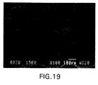
FIG. 19 shows an array of 8 mil pads with a 15 mil pitch on a Z-axis
material.
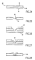
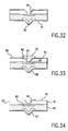
FIGS. 20-34 depict the process sequence for forming the laminated
wafer level contact sheet of the present invention.
FIG. 35 is a scanning electron micrograph of a bump formed on the
wafer level contact sheet of the present invention.
FIG. 36 shows an enlarged view of the via and surrounding photoresist
for form a conductive bump on the wafer level contact sheet of the present
invention.
FIG. 37 shows an isolated conductive bump and its dimensions.
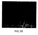
FIG. 38 shows a scanning electron micrograph of an ePTFE material
used for preparing an adhesive-filler composite.
The burn-in apparatus of the present invention includes: (1) a burn-in
substrate unit with a high planarity base; (2) a compliant, reusable, Z-axis
member unit. optionally containing an elastomer; and (3) a reusable, Z-axis
laminated wafer level contact sheet unit, in a stacked array, and its assembly.
The burn-in substrate unit, which contains circuitry layers on a lower portion or
surface thereof, and the wafer level contact sheet are electrically coupled to
one another when the compliant, reusable, Z-axis member unit is positioned
therebetween.
In FIG. 1 a semiconductor wafer 1 is shown having a plurality of chips 2
The wafer 1 can be a silicon wafer or any other suitable material such as.
germanium, silicon germanium, silicon carbide, gallium arsenide, selenium,
tellurium, InSb, BP, CdS, ZnSe, ZnTe, PbS, InP, PbSe, PbTe, InAs, GaSb, ZnS
and Bi2Te3. Each chip 2 on the wafer 1 has a plurality of contact pads 3 that
are brought into electrical contact with the test apparatus to be described
during testing. The chips 2 may be memory chips such as, but not limited to,
dynamic random access memories (DRAMS), application specific integrated
circuits (ASICS), analog chips, or any combination thereof. Chips 2 are
typically arranged in columns 4, or rows 5 on the wafer so that upon completion
of testing, the chips can be cut or "diced" from the wafer by sawing along the
channels. Subsequently, diced chips are used in applications by packaging
them in single chip modules (SCM), multi-chip module (MCM), or mounting
them directly on a printed circuit board (COB).
The pretesting mode of the burn-in apparatus of the present invention is
seen in FIG. 2. The burn-in apparatus 6 includes a base unit 7, a compliant.
selectively conductive Z-axis member 8 which may contain an elastomer, a
laminated wafer level contact sheet 9, a chuck 15 for receiving a semiconductor
wafer 1, and a test signal generator 10. The base unit 7 has a highly planar
structure and is positioned above the wafer 1, and extends beyond the edge or
edges of the wafer 1.
The base unit includes an upper surface 11 and a lower surface 12.
The lower surface 12 includes a plurality of first terminals 13 and second
terminals 14. The first terminals 13 and second terminals 14 are electrically
coupled together within the base unit 7.
The first terminals 13 are grouped in the center of the base unit 7,
above the wafer 1 having a corresponding pattern to the pattern of contact
pads of the chips 2 on the wafer 1. The second terminals 14 are also on the
lower surface 12 of the base unit 7, and are grouped outside of the periphery of
the first terminals 13. The second terminals 14 may form a ring around the first
terminals 13, may be grouped substantially on one side of the first terminals, or
may be distributed over the entire lower surface 12 of the base unit 7 outside of
the grouping of the first terminals 13. The second terminals 14 are connectable
to the test signal generator 10 at contacts.
A jig 16 encompasses the burn-in system and includes a mechanism 17
that can apply pressure to base 7 to engage Z-axis material 8 and contact
sheet 9 to have the bumps 18 thereon engage the pads of the wafer 1. The
bumps are best seen in FIGS. 34 and 35.
As shown schematically in FIG. 3, the connection between terminals 14
and generator 10 may be accomplished by raised members terminating in a
plurality of compressible pins 21, such as Pogo® pins or S shaped pins, on an
upper surface 20. The compressible pins 21 are electrically coupled through
the raised members to the test signal generator 10 and are arranged in a
mating pattern to the pattern of second terminals 14 on the base unit 7.
The laminated wafer level contact sheet 9 of the present invention may
be substantially the same size as the wafer 1 and has contact pads 20
arranged in a pattern corresponding to the first terminals 13 and the contact
pads 3 on the wafer 1. The terminals 13 are contact pads which are formed
from at least one metal layer, such as copper, nickel, gold, platinum, palladium
or cobalt, with a layer thickness of between 1 µm and 50 µm, and dimensions
of between 25 µm × 25 µm and 250 µm × 250 µm, and any desired shape.
The contact pads 20 on the surface of the laminated wafer level contact
sheet 9 are aligned to the first terminals 13 on the base unit 7 and are
temporarily attached to the lower surface of the base unit by the selectively
conductive member 8. The selectively conductive member 8 provides electrical
contact between the first terminals 13 of the base unit 7 and the contact pads
20 on the laminated wafer level contact sheet 9.
The wafer level contact sheet 9 also has raised bumps 18 on a lower
surface thereof that terminate in a tip having a diameter of 0.25 to 2.0 mils.
The raised bumps 18, best seen is FIGS. 34 and 35, are identified as reference
numeral 67. The raised bumps 18 have a pattern corresponding to the contact
pads 3 on the wafer 1 and are individually electrically coupled to the contact
pads 20 on the upper surface of the laminated wafer level contact sheet 9, best
seen in FIG. 34.
When a wafer 1 is place on the chuck 15, the wafer 1 is aligned so that
the pattern of contact pads 3 on the wafer 1 corresponds to the pattern of
raised bumps 18 on the laminated wafer level contact sheet 9. Alignment may
be accomplished by any of several techniques, including optical alignment,
infrared alignment, x-ray alignment, or mechanical alignment, such as, using
pits formed on the wafer level contact sheet 9 which mate to protrusions on the
wafer 1 (not shown). The wafer 1 may be held to the chuck 15 by a
mechanical jig 16 and 17, by creating a vacuum (not shown) between the wafer
1 and the chuck 15, or by mechanical coupling.
FIG. 3 depicts the burn-in apparatus of FIG. 2, wherein the raised
bumps 18 of the laminated wafer level contact sheet 9 have been brought into
intimate contact with the contact pads 3 of the wafer 1. Also, the second
terminals 14 on the base unit 7 have been brought into contact with the
compressible pins 21 on the test signal generator 10. Alternatively, contact
may be made by a piston which pushes the raised bumps of the burn-in device
against the contact pads 3 of the wafer 1 and the second terminals 14 against
the compressible pins 21 of the test signal generator 10. Contact may be
accomplished by creating a vacuum between the raised member of the test
signal generator and the base unit.
A heating element (not shown) may be included within the chuck 15 for
supplying heat to the wafer 1 in order to elevate the temperature of integrated
circuits on the chips 2 under test to a desired burn-in temperature. In cases of
high-power chips on the wafer, heat produced by the chips 2 under test may
elevate the temperature of the integrated circuits above the desired burn-in
temperature. In such a case, the wafer may be cooled by blowing cold air over
the wafer, by including a cooling element in the chuck 15, or by many other
known techniques. Alternatively, the entire jig may be located within a
temperature controlled environment to provide the elevated temperatures for
the burn-in procedures. Techniques for controlling temperature in
semiconductor manufacturing and testing are well known.
FIG. 4 depicts an alternate embodiment of the invention. wherein
compressive force applied to the burn-in device 6 is supplied by an inflatable
bladder 24 having a source of fluid (not shown) through valve conduit 25.
Inflation may be accomplished with liquid or a gas, and may tend to
compensate for any tilting of the burn-in device relative to the wafer under test
In an alternate embodiment of the invention, the test signal generator 10
may be coupled to the second terminals 14 by a variety of techniques, including
by a rigid connector or flexible conductive tape. The second terminals 14 may
be located on the surface 12 of the burn-in device, arranged in a pattern
substantially contained within the area of the wafer 1 below. In this scenario,
the burn-in device 6 itself might be no greater in size than the wafer itself.
BASE UNIT:
The base unit is best seen in FIG. 5 and includes a high planarity base
25 formed from low coefficient of thermal expansion (CTE) material or having a
matched composite CTE obtained through laminated layers of low and high
CTE material. The base unit includes a stack of good circuitry layers 26, each
layer includes a metal layer and a dielectric layer. Layer 27 of the base unit 7
includes dummy layers 27 which are used to balance circuitry layers 26. The
lower surface 28 includes the first and second terminals 13 and 14.
FIG. 6 depicts a base unit of the present invention which includes good
circuitry layers 32, a low CTE base 31 or base 31 having a low composite CTE
or matched CTE, and balancing layers 30. The base unit 29 has a pad layer
33, three signal layers 34, 36 and 37, a core layer 35, a low CTE base layer 31,
and balancing layers 30. Layers 33-37 form the "good" circuitry layers 26 of
base unit 29. Having three signal layers, 34, 36 and 37 facilitates routing a
large number of signals between the first and second terminals 13 and 14 of
the base unit 29. Positioning the core layer 35 between signal layers provides
predictable impedance for signal traces on each of the signal layers 34, 36, 37
and reduces electrical noise within the base unit 29. The low-CTE base 31
constrains thermal expansion of the base unit 29 and contributes to maintaining
high planarity of the base unit 29. Although the good layers 33-37 and
balancing layer 30 have 5 layers, more or less layers are possible.
The balancing layers 30 are preferably as numerous as the number of
"good" circuitry layers 26. The balancing layers should match the copper and
dielectric density of the corresponding layers within the "good" circuitry layers
26 on the opposite side of the low-CTE base 31. Matching the density on
opposing sides of the low CTE base 31 helps maintain the planarity of the base
unit 29.
The balancing layers 30 may not contribute at all to the electrical
performance of the base unit 29 and may be used entirely to maintain the
planarity of the base unit 29. Therefore, the balancing layers 30 may be
implemented with signal layers and core layers that have been scrapped due to
manufacturing defects but which have a substantially similar density to
corresponding "good" signal layers 34, 36, 37 and core layers 35 on the
opposite side of the low-CTE base. However, the balancing layers could be
additional "good" circuitization layers.
The core layer 35 is formed with a continuous sheet of conductive
material laminated to a dielectric layer. The conductive material can be half-ounce
copper, or one ounce copper. In place of copper, any metal having a
high CTE could be used, such as, but not limited to, stainless steels,
molybdenum, etc. The sheet of conductive material may be a substantially
continuous plane. or the sheet of conductive material may be a mesh. The
core layer 35 may be connected to the second terminals 14 and carry a voltage
such as power or ground to decouple noise from signal traces 43 on signal
layers 34, 36, 37 (shown in FIG. 8). Furthermore, the core layer 35 gives the
signal traces 43 above or below a predictable impedance based on the
dielectric constant of the dielectric, the geometry of the signal traces 43, and
the height of signal traces 43 above or below the metal plane of the core layer
35. The core layer 35 may be pierced by vias 41 (shown in FIG. 7) allowing
electrical coupling of signal layers 34, 36, 37 on opposite sides of the core layer
35. Furthermore, the core layer 35 may be coupled directly to the first
terminals 13 on the pad layer 33 through vias 41 to supply power or ground to
the wafer 1 under test.
In an alternate embodiment of the invention, the balancing layers 30
may be electrically incorporated into the base unit 29 by routing active signal
traces on the balancing layers, and coupling the signal traces to the first and
second terminals 13 and 14 by vias 41 through the low CTE base 31 or by a C-shaped
flex circuit spanning the upper and lower surfaces of the base unit 29.
Furthermore, the balancing layers 30 could support one or more active or
passive circuits which facilitate the burn-in testing of wafers.
FIG. 7 depicts an inverted view of the pad layer 33. The pad layer 33
has electrically conductive contact pads 38 disposed against a dielectric layer
39. The contact pads 38 are dispersed across a surface 40 of the dielectric
layer 39 of the pad layer 33 and implement the first and second terminals 13
and 14 of the base unit 7 or 29. Pads 38 may be raised above the surface of
the dielectric, as shown, and may have any desired shape including circular,
rectangular, conical, and trapezoidal. In one embodiment of the invention, the
contact pads 38 are circular and made of a lower layer of copper with an outer
coating of nickel or gold to resist corrosion and reduce contact resistance.
However, the outer material may be any noble metal, such as, but not limited
to, platinum or palladium. Similarly, the outer metal layer of contact pads 38
may also be any non-oxidative metal or metal alloy. The copper of the contact
pads 38 is preferably formed from a base copper foil by a subtractive etch
process well known in the art. Subsequently, an outer coating may be formed
onto the copper using any technique including plating by an electrolytic or
electroless process. Vias 41 are shown formed in the dielectric layer 39 of the
pad layer 33 beneath the contact pads 38. Vias holes 41 may be formed in the
dielectric layer 39 by many known techniques including drilling and laser
ablation.
Generally, various ePTFE-based dielectric materials can be laser drilled
using mode-locked solid states lasers operating in the UV range, and in
particular, those capable of producing energy densities in the range of 0.5 to 20
J/cm2 and those capable of making in-situ and virtually instantaneous changes
in the energy density by varying the pulse repetition rate from 1000 to 10000
Hz. These variations in pulse repetition rate result in variations in the pulse
width for Nd:YAG lasers of between 40 and 100 ns. In general, when
performing a post-pulse step to ablate dielectric residue after an initial ablation
step, the pulse density can be double for a brief time period, whereby 1-10
pulses may typically
In one embodiment of the present invention, the blind vias are formed
with lasers that are solid state pulsed lasers such as the pulsed Nd:YAG laser.
The fundamental output from the Nd:YAG laser is at a wavelength of 1064 nm.
This wavelength is in the infrared portion of the electromagnetic spectrum. By
installing beta-Barium Borate (BBO) crystals in the optical path harmonic
generation facilitates the output of light at 355 nm (third harmonic) and 266 nm
(fourth harmonic), which fall in the ultraviolet range.
The 355 nm and 266 nm wavelengths are particularly well suited for
drilling vias in the laminated substrates of the present invention. The pulse
length, energy density and number of pulses can be varied depending on the
type of via being formed and the type of materials used in the laminated
substrate.
For example, for drilling blind vias in a laminated substrate made of
alternating layers of copper and an adhesive-filler-ePTFE dielectric, and using a
266 nm laser, the energy density is 1.5 J/cm2, the energy per pulse is 10 µJ,
and the power density is 20 megawatts per cm2. At the 355 nm wavelength,
blind vias are formed by setting the energy density at 3.5 J/cm2, the energy per
pulse is 30 µJ, and the power density is 35 megawatts per cm2. The post-pulse
step for the 355 nm blind via requires adjusting the conditions such that the
energy density is 11 J/cm2, the energy per pulse is 100 µJ, and the power
density is 200 megawatts per cm2.
When forming blind vias in the adhesive-filler-ePTFE dielectric, using
the 355 nm laser, the energy density is 7 J/cm2, the energy per pulse is 65 µJ,
and the power density is 100 megawatts per cm2. A post-pulse step would
require adjusting the parameters such that the energy density is 11 J/cm2, the
energy per pulse is 100 µJ, and the power density is 200 megawatts per cm2.
be used.
The via holes 41 may then be plated with a metal, for example copper,
to create a conductive path from the contact pads 38 on the upper surface 40
of the pad layer 33 to the lower surface 42 of the pad layer 33.
One or more signal layers, 34, 36, 37 is disposed above the pad layer
33. However, the pad layer 33 is optional and the contact pads 38 described
as part of the pad layer 33 above may be implemented directly on the signal
layer 34. The signal layers 34, 36, 37 comprise a plurality of conductive
segments or signal traces 93 distributed across a dielectric layer as shown in
FIG. 8.
As seen in FIG. 8, the signal traces 43 create a conductive path 44
between the first terminals 13 and the second terminals 14 of the base unit 7 or
29. The signal traces 43 are typically and preferably copper, formed by a
process of subtractive etching. A complete conductive path from the first
terminals 13 to the second terminals 14 may be formed by creating a path from
a first terminal 13, up through a via hole 91 (not shown) in the dielectric layer
39 of the pad layer 33 to a signal trace 93 on a signal layer, across the signal
trace 93 of the signal layer to another via hole going down through the dielectric
of the pad layer 33 to a corresponding second terminal 14. Similarly. first and
second terminals 13 and 14 may be electrically connected by a more complex
path of signal traces 43 and vias 41 spanning multiple signal layers.
FIG. 9 depicts the low CTE base 31 according to one embodiment of
the invention. The base 31 is formed from a three ply stack of INVAR 36,
copper and INVAR 36, respectively layers 45, 46 and 47. Instead of INVAR 36,
a nickel and iron alloy containing between 30 wt.% and 42 wt.% nickel may
also be used. Additionally, in place of INVAR 36 and layers 45 and 47, any low
CTE material matched to the wafer unit test device, including but not limited to
nickel alloys, may be used. The two nickel alloy sheets have a combined
thickness t 1 and the copper sheet 46 has a thickness t 2 , wherein a ratio t 1 to t 2
is chosen to match the coefficient of thermal expansion of a semiconductor
wafer. The t 1 to t 2 ratio can be between 4:1 and 14:1, including, but not limited
to ratios of 10:1, 11:1 and 12:1.
In one embodiment of the present invention, the nickel layers each have
a thickness of approximately 115 mils, and the ratio of the nickel layers to the
copper layer provides a coefficient of thermal expansion that matches a silicon
wafer. However, the ratio of the nickel layer thickness, or other material
thickness, to the copper layer thickness provides a coefficient of thermal
expansion for the base that matches the coefficient of thermal expansion for a
wafer formed from germanium, silicon germanium, silicon carbide, gallium
arsenide, selenium and tellurium.
Nickel alloys have a low coefficient of thermal expansion, and therefore
act to constrain the expansion of the base unit 31 relative to the wafer 1 as
temperature increases. Preferably a fourteen inch square sheet of INVAR 36
and copper material are used. However, circular or rectangular sheets may be
used. The sheets are between six and twenty inches in dimension, i.e.,
diameter or side length, such as, eight, twelve, fourteen, sixteen and twenty
inches.
The INVAR 36 and sheets 45 and 47 are each preferably machined to
approximately 115 mils thick with a degree of planarity between 0 020 and
0.0001 inches per linear foot, preferably between 0.01 and 0 0001 inches per
linear foot. Most preferably, the degree of planarity is 0 001 inches per linear
foot.
The copper layer 46 is approximately 21 mils thick and has a planarity
of 0.0005 inches per linear foot. The copper layer comprises approximately
8% to 10%, e.g., 9.1%, of the total thickness of said metal or metal alloy layers
and said copper layer
The stack of INVAR 36, copper, and INVAR 36 is formed by laminating
each piece of INVAR 36 to a surface of the copper using a dielectric 48, such
as Speedboard® C, which is available from W. L. Gore and Associates, and
which is described below. The dielectric layers of the low CTE base are
between 25 µm and 250 µm thick.
Sheet thicknesses of 115 mils and 21 mils of the nickel alloy and
copper sheets respectively are used in one embodiment, but any dimensions
may be chosen, so long as the thickness of nickel alloy sheets is greater than
the thickness of the copper.
DIELECTRIC:
The dielectric materials used for the base unit and wafer level contact
sheet of the present invention can be any high temperature dielectric material.
For example, suitable dielectric materials include, but are not limited to
polyimides and polyimide laminates, epoxy resins, organic materials, or
dielectric materials comprised at least in part of polytetrafluoroethylene, with or
without a filler, where once the adhesive has been impregnated, it has been
partially cured and forms a B-stage material. Suitable materials include
Speedboard® bond plies available from W. L. Gore and Associates, Inc. As
should be understood, Speedboard® C does not contain a ceramic filler and is
a prepreg of non-woven material containing a cyanate ester resin in a
polytetrafluoroethylene matrix. Speedboard C® has a dielectric constant, (Dk)
of about 2.6-2.7 at 1MHz-10GHz, a loss tangent of 0.004 at 1MHz-10GHz, a
dielectric strength greater than 1000 V/mil, a glass transition and a Tg of 220°C,
a resin content of 66-68 wt.% and is available in a variety of thicknesses.
Other classes of dielectric materials include those where a porous matrix
system contains an imbibed or impregnated adhesive-filler mixture. The porous
matrix is a non-woven substrate that is imbibed with high quantities of filler and a
thermoplastic or thermoset adhesive, as a result of the initial void volume of the
substrate, heated to partially cure the adhesive and form a B-stage composite.
Substrates include fluoropolymers, such as the porous expanded
polytetrafluoroethylene material of U S. Patent Nos. 3.953,566 to Gore and
4,482,516 to Bowman, et al., each of which is incorporated herein by reference.
Desirably, the mean flow pore size (MFPS) should be between about 2 to 5 times
or above that of the largest particulate, with a MFPS of greater than about 2.4
times that of the filler being particularly preferred. However, it is also within the
scope of the invention that suitable composites can be prepared by selecting the
mean flow particle size MFPS to average particle size ratio to be greater than 1.4.
Acceptable composites can also be prepared when the minimum pore size to
average particle size is at least above 0.8 or the minimum pore size to the
maximum particle size is at least above 0.4. The MFPS to particle size ratio
ratios being performed with a microtrak FRA analyzer.
Alternatively, another mechanism for gauging relative pore and particle
sizes may be calculated as the smallest pore size being not less than about 1.4
times the largest particle size.
In addition to expanded fluoropolymer substrates, porous expanded
polyolefins, such as ultra high molecular weight (UHMW) polyethylene, expanded
polypropylene, polytetrafluoroethylene made prepared by paste extrusion and
incorporating sacrificial fillers, porous inorganic or organic foams, microporous
cellulose acetate, can also be used.
The porous substrate has an initial void volume of at least 30%,
preferably at least 50%, and most preferably at least 70%, and facilitates the
impregnation of thermoset or thermoplastic adhesive resin and particulate filler
paste in the voids while providing a flexible reinforcement to prevent brittleness of
the overall composite and settling of the particles.
The filler comprises a collection of particles when analyzed by a
Microtrak® Model FRA Partical Analyzer device, which displays a maximum
particle size, a minimum particle size and an average particle size by way of a
histogram.
Suitable fillers to be incorporated into the adhesive include, but are not
limited to, BaTiO3, SiO2, Al2O3, ZnO, ZrO2, TiO2, precipitated and sol-gel
ceramics, such as silica, titania and alumina. non-conductive carbon (carbon
black) and mixtures thereof. Especially preferred fillers are SiO2, ZrO3, TiO2
alone or incombination with non-conductive carbon. Most preferred fillers include
filler made by the vapor metal combustion process taught in U.S. Patent No.
4.705.762, such as, but not limited to silicon, titanium and aluminum to produced
silica, titania, and alumina particles that are solid in nature, i.e., not a hollow
sphere, with a uniform surface curvature and a high degree of sphericity.
The fillers may be treated by well-known techniques that render the filler
hydrophobic by silylating agents and/or agents reactive to the adhesive matrix,
such as by using coupling agents. Suitable coupling agents include, silanes,
titanates, zirconates, and aluminates. Suitable silylating agents may include,
but are not limited to, functional silyating agents, silazanes, silanols, siloxanes.
Suitable silazanes, include, but are not limited to, hexamethyldisilazane (Huls
H730) and hexamethylcyclotrisilazane, silylamides such as,
bis(trimethylsilyl)acetamide (Huls B2500), silylureas such as trimethylsilylurea,
and silylmidazoles such as trimethylsilylimidazole.
Titanate coupling agents are exemplified by the tetra alkyl type,
monoalkoxy type, coordinate type, chelate type, quaternary salt type,
neoalkoxy type, cycloheteroatom type. Preferred titanates include, tetra alkyl
titanates, Tyzor® TOT {tetrakis(2-ethyl-hexyl) titanate, Tyzor® TPT
{tetraisopropyl titanate}, chelated titanates, Tyzor® GBA {titanium
acetylacetylacetonate}, Tyzor® DC {titanium ethylacetacetonate}, Tyzor® CLA
{proprietary to DuPont}, Monoalkoxy (Ken-React® KR TTS), Ken-React®, KR-55
tetra (2,2 diallyloxymethyl)butyl, di(ditridecyl)phosphito titanate, LICA® 38
neopentyl(diallyl)oxy, tri(dioctyl)pyro-phosphato titanate.
Suitable zirconates include, any of the zirconates detailed at page 22 in
the Kenrich catalog, in particular KZ 55- tetra (2.2 diallyloxymethyl)butyl,
di(ditridecyl)phosphito zirconate, NZ-01- neopentyl(diallyl)oxy, trineodecanoyl
zirconate, NZ-09-neopentyl(diallyl)oxy, tri(dodecyl)benzene-sulfonyl zirconate.
The aluminates that can be used in the present invention include, but
are not limited to Kenrich®, diisobutyl(oleyl)acetoacetylaluminate (KA 301),
diisopropyl(oleyl)acetoacetyl aluminate (KA 322) and KA 489.
In addition to the above, certain polymers, such as, cross-linked vinylic
polymers, e.g., divinylbenzene, divinyl pyridine or a sizing of any of the
disclosed thermosetting matrix adhesives that are first applied at very high
dilution (0.1 up to 1.0% solution in MEK) can be used. Also, certain organic
peroxides, such as. dicumylperoxide can be reacted with the fillers.
The adhesive itself may be a thermoset or thermoplastic and can
include polyglycidyl ether, polycyanurate, polyisocyanate. bis-triazine resins,
poly (bis-maleimide), norbornene-terminated polyimide, polynorbornene,
acetylene-terminated polyimide, polybutadiene and functionalized copolymers
thereof, cyclic olefinic polycyclobutene, polysiloxanes,
functionalized polyphenylene ether, polyacrylate, novolak polymers and
copolymers, fluoropolymers and copolymers, melamine polymers and
copolymers, poly(bis phenycyclobutane), and blends or prepolymers thereof. It
should be understood that the aforementioned adhesives may themselves be
blended together or blended with other polymers or additives, so as to impact
flame retardancy or enhanced toughness.
As used herein, Mean Flow Pore Size and minimum pore size were
determined using the Coulter® Porometer II (Coulter Electronics Ltd., Luton
UK) which reports the value directly. Average particle size and largest particle
size were determined using a Microtrac light scattering particle size analyzer
Model No. FRA (Microtrac Division of Leeds & Northup, North Wales, PA,
USA). The average particle size (APS) is defined as the value at which 50% of
the particles are larger. The largest particle size (LPS) is defined as the largest
detectable particle on a Microtrac histogram. Alternatively, the largest particle
size is defined at the minimum point when the Microtrak FRA determines that
100% of the particulate have passed.
In general, the method for preparing the adhesive-filler dielectric
involves:(a) expanding a polytetrafluoroethylene sheet by stretching a
lubricated extruded preform to a microstructure sufficient to allow small
particles and adhesives to free flow into the void or pore volume; (b) forming a
paste from polymeric, e.g., thermoset or thermoplastic material and a filler: and
(c) imbibing by dipping, coating, pressure feeding, the adhesive-filler paste into
the highly porous scaffold, such as expanded polytetrafluoroethylene.
To prepare the filled adhesive film of this invention, particulate filler is
mixed into a solvent or aqueous solution or molten adhesive to afford a finely
dispersed mixture. The filler in small particle form is ordinarily less than 40
microns in size, and preferably has an average particulate size between 1 and
10 microns. The mean pore size of the node-and-fibril structure of the
polytetrafluoroethylene should be large enough to allow for adequate
penetration of the particulate. If the substrate is. to be expanded
polytetrafluoroethylene, then structures similar to those taught in U.S. Patent
No. 4,482,516 to Bowman, et al. are desirable. Desirably, the mean flow pore
size (MFPS) should be between about 2 to 5 times or above that of the largest
particulate. with a MFPS of greater than about 2.4 times that of the filler being
particularly preferred. However, it is also within the scope of the invention that
suitable composites can be prepared by selecting the mean flow pore size
MFPS to average particle size ratio to be greater than 1.4. Acceptable
composites can also be prepared when the minimum pore size to average
particle size is at least above 0 8 or the minimum pore size to the maximum
particle size is at least above 0.4. The MFPS to particle size ratio ratios being
performed with a microtrak FRA analyzer.
Alternatively, another mechanism for gauging relative pore and particle
sizes may be calculated as the smallest pore size being not less than about 1.4
times the largest particle size.
Table 1 shows the effect of the relationship of the substrate mean flow
pore size (MFPS) and particulate size. When the ratio of the mean flow pore
size (MFPS) to largest particulate is 1.4 or less, poor results are observed. In
this case, a homogeneous composite is not observed, and most of the
particulate filler does not uniformly penetrate the microporous substrate. When
" the ratio of the MFPS to largest particulate is greater than about 2.0, then a
uniform composite is obtained. It is also observed that the larger the ratio of
MFPS to largest particulate, the greater the relative case it is to imbibe a
homogeneous dispersion into the microporous substrate.
| Sample | Substrate Pore Size | Particle Size | MFPS ÷ PartAvg | PoreMin ÷ PartMax | PoreMin ÷ PartAvg | Result |
| | Min (µm) | MFPS (µm) | Avg (µm) | Max (µm) |
| A | 4 | 7 | 5 | 10 | 1.4 | 0.4 | 0.8 | Poor |
| B |
| | 4 | 5 | 5 | 10 | 1.0 | 0.4 | 0.8 | Poor |
| C | -- | 58 | 5 | 10 | 12.4 | N/A | - | Good |
| D |
| | 18 | 32 | 6 | 10 | 5.3 | 1.8 | 3.0 | Good |
| E |
| | 18 | 32 | 1 | 1 | 32.0 | 18.0 | 18 | Good |
| F |
| | 17 | 24 | 6 | 10 | 4.0 | 1.7 | 28 | Good |
| G | 0.2 | 0.4 | 0.5 | 1.6 | 0.8 | 0.125 | 0.4 | Poor |
| H | -- | 60 | 18 | 30 | 3.3 | -- | - | Good |
| I |
| | 14 | 11 | 0.5 | 1.6 | 22.0 | 8.8 | 28 | Good |
| J |
| | 14 | 29 | 4 | 8 | 7.3 | 1.8 | 3.5 | Good |
| K |
| | 14 | 29 | 5 | 10 | 5.8 | 1.4 | 2.8 | Good |
A fine dispersion was prepared by mixing 281.6 g TiO2 (TI Pure R-900,
Du Pont Company) into a 20% (w/w) solution of a flame retarded
dicyanamide/2-methylimidazole catalyzed bisphenol-A based polyglycidyl ether
(Nelco N-4002-5, Nelco Corp.) in MEK. The dispersion was constantly agitated
so as to insure uniformity. A swatch of expanded PTFE was then dipped into
the resin mixture. The web was dried at 165°C for 1 min. under tension to
afford a flexible composite. The partially-cured adhesive composite thus
produced comprised of 57 weight percent TiO2, 13 weight percent PTFE and
30 weight percent epoxy adhesive. Several plies of the adhesive sheet were
laid up between copper foil and pressed at 600 psi in a vacuum-assisted
hydraulic press at temperature of 225°C for 90 min. then cooled under
pressure. This resulted in a copper laminate having dielectric constant of 19.0,
and withstood a 30 sec. solder shock at 280°C at an average ply thickness of
100 µm (0.0039"(3.9 mil)) dielectric laminate thickness.
EXAMPLE 2
A fine dispersion was prepared by mixing 386 g SiO2 (HW-11-89,
Harbison Walker Corp.) which was pretreated with phenyltrimethoxysilane
(04330, Huls/Petrarch) into a manganese catalyzed solution of 200 g
bismaleimide triazine resin (BT206OBJ, Mitsubishi Gas Chemical) and 388 g
MEK. The dispersion was constantly agitated so as to insure uniformity. A
swatch of 0.0002" thick expanded PTFE was then dipped into the resin mixture,
removed, and then dried at 165°C for 1 min. under tension to afford a flexible
composite. Several plies of this prepreg were laid up between copper foil and
pressed at 250 psi in a vacuum-assisted hydraulic press at temperature of
225°C for 90 min. then cooled under pressure. This resulting dielectric thus
produced comprised of 53 weight percent SiO2, 5 weight percent PTFE and 42
weight percent adhesive, displayed good adhesion to copper, dielectric
constant (at 10 GHz) of 3.3 and dissipation factor (at 10 GHz) of 0.005.
EXAMPLE 3
A fine dispersion was prepared by mixing 483 g SiO2 (HW-11-89) into a
manganese-catalyzed solution of 274.7 g bismaleimide triazine resin
(BT2060BJ, Mitsubishi Gas Chemical) and 485 g MEK. The dispersion was
constantly agitated so as to insure uniformity. A swatch of 0.0002" thick
expanded PTFE was then dipped into the resin mixture, removed, and then
dried at 165°C for 1 min. under tension to afford a flexible composite. Several
plies of this prepreg were laid up between copper foil and pressed at 250 psi in
a vacuum-assisted hydraulic press at temperature of 225°C for 90 minutes then
cooled under pressure. The resulting dielectric thus produced comprised of 57
weight percent SiO2, 4 weight percent PTFE and 39 weight percent adhesive.
displayed good adhesion to copper, dielectric constant (at 10 GHz) of 3 2 and
dissipation factor (at 10 GHz) of 0.005.
EXAMPLE 4
A fine dispersion was prepared by mixing 15.44 kg TiO2 powder (TI
Pure R-900. DuPont Company) into a manganese-catalyzed solution of 3.30 kg
bismaleimide triazine resin (BT206OBH, Mitsubishi Gas Chemical) and 15.38
kg MEK. The dispersion was constantly agitated so as to insure uniformity. A
swatch of 0.0004" TiO2-filled expanded PTFE (filled according to the teachings
of Mortimer U.S. Patent No. 4,985,296, except to 40% loading of TiO2 and the
membrane was not compressed at the end) was then dipped into the resin
mixture, removed, and then dried at 165°C for 1 min. under tension to afford a
flexible composite. The partially cured adhesive composite thus produced
comprised of 70 weight percent TiO2. 9 weight percent PTFE and 21 weight
percent adhesive Several plies of this prepreg were laid up between copper
foil and pressed at 500 psi in a vacuum-assisted hydraulic press at temperature
of 220°C for 90 minutes then cooled under pressure. This resulting dielectric
displayed good adhesion to copper, dielectric constant of 10.0 and dissipation
factor of 0.008.
EXAMPLE 5
A fine dispersion was prepared by mixing 7.35 kg SiO2 (ADMATECHS
SO-E2, Tatsumori LTD) with 7.35 kg MEK and 73.5 g of coupling agent, i.e.,3-glycidyloxypropyltri-methoxysilane
(Dynasylan GLYMO (Petrach Systems).
SO-E2 is described by the manufacture as having highly spherical silica having
a particle diameter of 0.4 to 0.6 µm, a specific surface area of 4-8m2/g, a bulk
density of 0.2-0.4 g/cc (loose).
To this dispersion was added 932 g of a 50% (w/w) solution of a
cyanated phenolic resin, Primaset PT-30 (Lonza Corp.). in (MEK)
methylethylketone, 896 g of a 50% (w/w) solution of RSL 1462 (Shell Resins,
Inc.(CAS #25068-38-6)) in MEK, 380 g of a 50% (w/w) solution of BC-58 (Great
Lakes, Inc.) in MEK, 54 g of 50% solution of bisphenol A (Aldrich Company) in
MEK, 12.6 g Irganox 1010 (Ciba Geigy), 3.1 g of a 0.6% solution of Manganese
2-ethylhexanoate (Mn HEX-CEM (OMG Ltd.), and 2.40 kg MEK. This
dispersion was subjected to ultrasonic agitation through a Misonics continuous
flow cell for about 20 minutes at a rate of about 1-3 gal./minute. The fine
dispersion thus obtained was further diluted to an overall bath concentration of
11.9% solids (w/w).
The fine dispersion was poured into an impregnation bath. A expanded
polytetrafluoroethylene web had the node fibril structure of
FIG. 5, and the
following properties:
| Frazier | 20.55 |
| Coverage | 9 g/m2 |
| Ball Burst | 3.2 lbs. |
| Thickness | 6.5 mil. |
| Mean Flow Pore Size | 9.0 microns |
The Frazier number relates to the air permeability of the material being
assayed. Air permeability is measured by clamping the web in a gasketed
fixture which is provided in circular area of approximately 6 square inches for
air flow measurement. The upstream side was connected to a flow meter in
line with a source of dry compressed air. The downstream side of the sample
fixture was open to the atmosphere. Testing is accomplished by applying a
pressure of 0.5 inches of water to the upstream side of the sample and
recording the flow rate of the air passing through the in-line flowmeter (a ball-float
rotameter that was connected to a flow meter.
The Ball Burst Strength is a test that measures the relative strength of
samples by determining the maximum at break. The web is challenged with a
1 inch diameter ball while being clamped between two plates. The Chatillon,
Force Gauge Ball/Burst Test was used. The media is placed taut in the
measuring device and pressure affixed by raising the web into contact with the
ball of the burst probe. Pressure at break is recorded.
The web described above was passed through a constantly agitated
impregnation bath at a speed at or about 3 ft./min, so as to insure uniformity.
The impregnated web is immediately passed through a heated oven to remove
all or nearly all the solvent, and is collected on a roll.
Several plies of this prepeg were laid up between copper foil and
pressed at 200 psi in a vacuum-assisted hydraulic press at temperature of
220°C for 90 minutes and then cooled under pressure This resulting dielectric
displayed good adhesion to copper, dielectric constant (10 GHz) of 3.0 and
dissipation factor of 0.0085 (10 GHz).
The physical properties of the particulate filler used in Example 4 and
Example 7 are compared below.
| Property | Tatsumori (ADMATECHS) | Harbison Walker |
| Manufacture Technique | Vapor Metal Combustion | Amorphous Fused Silica |
| Designation | Silica SO-E2 | HW-11-89 |
| Median Particle Size | 0.5 micron | 5 micron |
| Shape | Spherical | Irregular, jagged |
| Surface Area | 6-10 m2/g | 10 m2/g |
| Bulk Density | 0.47 g/cc | 1.12 g/cc |
| Specific Density | 2.26 g/cc | 2.16 g/cc |
An ePTFE matrix containing an impregnated adhesive filler mixture.
based on SiO2 prepared from the vapor combustion of molten silicon is
prepared as follows. Two precursor mixtures were initially prepared. One
being in the form of a slurry containing a silane treated silica similar to that of
Example 5 and the other an uncatalyzed blend of the resin and other
components.
Mixture I
The silica slurry is a 50/50 blend of the SO-E2 silica of Example 5 in
MEK, where the silica contains a coated of silane which is equal to 1% of the
silica weight. To a five gallon container, 17.5 pounds of MEK and 79 grams of
silane were added and the two components mixed to ensure uniform dispersion
of the silane in the MEK. Then, 17.5 pounds of the silica of Example 5 were
added. Two five gallon containers of the MEK-silica-silane mixture were added
to a reaction vessel, and the contents, i.e., the slurry, was recirculated through
an ultrasonic disperser for approximately one hour to break up any silica
agglomerates that may be present. The sonication was completed and the
contents of the reaction vessel were heated to approximately 80°C for
approximately one hour. while the contents were continuously mixed. The
reacted mixture was then transferred into a ten gallon container.
Mixture II
The desired resin blend product is an MEK based mixture containing an
uncatalyzed resin blend (the adhesive) contains approximately 60% solids,
where the solid portion is an exact mixture of 41.2% PT-30 cyanated phenolic
resin, 39.5% RSL 1462 epoxy resin, 16.7% BC58 flame retardant, 1 5%
Irganox 1010 stabilizer, and 1% bisphenol A co-catalyst, all percentages by
weight.
Into a ten gallon container, 14.8 pounds of PT-30 and 15-20 pounds of
MEK were added and stirred vigorously to completely solvate the PT-30. Then
6 pounds of BC58 were measured and added to the MEK/PT-30 solution and
vigorously agitated to solvate the BC58. The stabilizer, 244.5 grams of Irganox
1010 and bisphenol A, 163 grams were added. The ten gallon container was
reweighed and 14.22 pounds of RSL 1462 were added. Additional MEK was
added to bring the mixture weight to 60 pounds. The contents were then
vigorously agitated for approximately 1 to 2 hours, or as long is necessary to
completely dissolve the solid components.
The desired product is a mixture of the silica treated with a silane, the
uncatalyzed resin blend, and MEK in which 68% by weight of the solids are
silica, and the total solids are between 5% and 50% by weight of the mixture.
The exact solids concentration varies from run to run, and depends in part on
the membrane to be impregnated. The catalyst level is 10 ppm relative to the
sum of the PT-30 and RSL1462.
The solid contents of mixtures I and II were determined to verify the
accuracy of the precursors and compensate for any solvent flash that had
occurred. Then mixture I was added to a ten gallon container to provide 12
pounds of solids, e.g., 51.5% solids content, 23.48 pounds of mixture I. Then
mixture II was added to the container to provide 5.64 pounds of solids, e.g.,
59.6% solids, 9.46 pounds of mixture II. the manganese catalyst solution
(0.6% in mineral spirits), 3.45 grams, was added to the mixture of mixture I and
mixture II and blended thoroughly to form a high solids content mixture
The bath mixture for impregnating an ePTFE matrix, 28% solids
mixture, was prepared by adding sufficient MEK to the high solids content
mixture to a total weight of 63 pounds.
Thereafter. an ePTFE matrix weas impregnated with this bath mixture to
form a dielectric material.
EXAMPLE 7
A fine dispersion was prepared by mixing 26.8 grams Furnace Black
(Special Schwarz 100. Degussa Corp., Ridgefield Park, New Jersey) and 79
grams of coupling agent (Dynaslan GLYMO CAS #2530-83-8; 3-glycidyloxypropyl-trimethoxysilane
(Petrach Systems). The dispersion was
subjected to ultrasonic agitation for 1 minute, then added to a stirring dispersion
of 17.5 pounds SiO2 (SO-E2) in 17.5 pounds MEK which had previously been
ultrasonically agitated. The final dispersion was heated with constant overhead
mixing for 1 hour at reflux, then allowed to cool to room temperature.
Separately, an adhesive varnish was prepared by adding the following:
3413 grams of a 57.5% (w/w) mixture of Primaset PT-30 in MEK, 2456 grams
of a 76.8% (w/w/) mixture of RSL 1462 in MEK, 1495 grams of a 53.2% (w/w)
solution of BC58 (Great Lakes, Inc.) in MEK. 200 grams of 23.9% (w/w)
solution of bisphenol A (Aldrich Company) in MEK, 71.5 grams Irganox 1010,
3.21 grams of a 0.6% (w/w) solution of Mu HEX-CEM (OMG Ltd.) in mineral
spirits, and 2.40 kg MEK.
In a separate container, 3739 grams of the dispersion described above
was added, along with 0.0233 grams of Furnace Black (Special Schwarz 100,
Degussa Corp., Ridgefield Park, New Jersey), 1328 grams of the adhesive varnish
described above and 38.3 pounds MEK. This mixture was poured into an
impregnation bath, and an ePTFE web was passed through the impregnation
bath at a speed at or about 3 ft/min. This dispersion was constantly agitated so
as to insure uniformity. The impregnated web is immediately passed through a
heated oven to remove all or nearly all the solvent, and is collected on a roll.
Several piles of this prepeg were laid up between copper foil and
pressed at 200 psi in a vacuum-assisted hydraulic press at temperatures of
200°C for 90 minutes then cooled under pressure This resulting dielectric
displayed good adhesion to copper.
EXAMPLE 8
An adhesive varnish was prepared by adding the following: 3413 grams
of a 57.5% (w/w) solution of Primaset PT-30 (PMN P-88-1591)) in MEK. 2456
grams of a 76.8% (w/w) solution of RSL 1462 in MEK, 1495 grams of a 53.2%
(w/w) solution of BC58 (Great Lakes, Inc.) in MEK, 200 grams of 23.9% (w/w)
solution of bisphenol A (Aldrich Company) in MEK, 71.5 grams Irganox 1010,
3.21 grams of a 0.6% (w/w) solution of Mn HEX-CEM in mineral spirits, and
2.40 kg MEK.
In a separate container, 1328 grams of the adhesive varnish described
above, was added along with 42.3 pounds MEK, 6.40 grams of Furnace Black
(Special Schwarz 100, Deguss Corp., Ridgefield, New Jersey) and 1860.9 grams
SiO2(SO-E2). This mixture was poured into an impregnation bath, and an ePTFE
web was passed through the impregnation bath at a speed at or about 3ft/min.
The dispersion was constantly agitated so as to insure uniformity. The
impregnated web is immediately passed through a heated oven to remove all or
nearly all the solvent, and is collected on a roll.
Several piles of this prepeg were laid up between copper foil and
pressed at 200 psi in a vacuum-assisted hydraulic press at temperature of
220°C for 90 minutes then cooled under pressure. This resulting dielectric
displayed good adhesion to copper.
The low CTE base of FIG. 9 was prepared using the dielectric material
of Example 6. A copper core was laminated on each side thereof with a layer
of the filled ePTFE of FIG. 9. Thereafter, INVAR 36 is placed on each exposed
side of the dielectric material. The composite is heated under pressure to form
the base unit 31.
As discussed above with reference to FIGS. 1 and 2, a Z-axis material
is used for components 2 and 9. The selectively conductive Z-axis substrate
member is reusable and compliant. As taught in U.S. Patent No. 5.498,467 to
Meola, the basic substrate is a planar, open cell, porous material lying in a
plane defined by an x and a y-axis, and having Z-axis pathways extending from
one side of the material to the other side. When the Z-axis material includes an
optional elastomer, it is positioned between the lower surface 12 of the base
unit 7 and the upper surface of the laminated wafer level contact sheet 9. The
selectively conductive member 8. having the optional elastomer, has a series of
electrically isolated, irregularly shaped electrically conductive pathways
extending from a lower surface of the selectively conductive member to an
upper surface generally in the direction of the Z-axis When in place between
the base unit 7 and the laminated wafer level contact sheet 9. the electrically
conductive pathways electrically couple the first terminals 13 of the base unit 7
to the contact pads 20 on the upper surface of the laminated wafer level
contact sheet 9.
When the Z-axis material is used to form the laminated wafer level
contact sheet 9, to be described hereinafter, it contains an bonding adhesive
which is in the partially cured, B-stage. However, because it is in contact with
the Z-axis material 8. is may be readily detached therefrom and be reused to
attach another wafer level contact sheet 9.
Suitable materials for the Z-axis member, which can be used for both
the material 8 and laminated wafer level contact sheet 9, have a thickness on
the order of 5×10⁻⁶m and 5×10⁻⁴m (5 µm and 500 µm), e.g, 50 µm, 75 µ, 100
µm, 150 µm etc., and include woven or non-woven fabric, such as a nylon
glass fiber or polyester fabric or cotton, or the like. The member can also be a
porous polymeric material or membrane, that is flexible, such as porous
polyolefins, e.g., porous polyethylene, porous polypropylene, porous
fluoropolymers, or open cell, porous polyurethanes. Additionally, open cell,
porous inorganic materials, such as thin porous ceramic plates that have
continuous pores from one side to the other can be used.
Porous fluoropolymers include, but are not limited to, porous
polytetrafluoroethylene (PTFE), porous expanded polytetrafluoroethylene
(ePTFE), porous copolymers of polytetrafluoroethylene and polyesters or
polystyrenes, copolymers of tetrafluoroethylene and fluorinated ethylene
propylene (FEP) or perfluoroalkoxy-tetrafluoroethylene (PFA) with a C1-C4
alkoxy group. Porous materials include expanded polypropylene, porous
polyethylene and porous polytetrafluoroethylene.
The material used as the substrate for the Z-axis material is expanded
polytetrafluoroethylene having a microstructure of nodes interconnected with
fibrils, a void volume of about 20% to 90%, such as the material prepared in
accordance with the teachings of U.S. Patent No. 3,953,566, incorporated
herein by reference, exemplified by the ePTFE of FIG. 11.
A planar porous material that is used as the Z-axis substrate has a
thickness of between about 5 and 125 µm, but thickness is not a critical factor
so long as the ultra-violet strength used to form the conductive pathways will
penetrate the sample
With reference to FIGS. 10-13, when the material for forming the Z-axis
member is microporous PTFE (expanded polytetrafluoroethylene), the pores 49
are defined as the space between nodes 50 interconnected with fibrils 51, as
shown in FIG. 10 In this case, the internal structure of nodes 50
interconnected with fibrils 51 is of a material density that results in an irregular
continuous path 52 through the Z axis within a vertically defined cross section
of the Z axis from one side of the planar member to the other (see FIG. 13).
The selectively conductive member 53 (FIG. 13) is prepared by making
areas 32 (FIG. 12) through the Z-axis direction receptive to deposition of a
metal salt, which metal salt on exposure to radiant energy is converted to
nonconductive metal nuclei which then act to catalyze deposition of a
conductive metal from an electroless metal deposition solution. The pores 49
of a porous member, defined above, are first wetted with a wetting agent, such
as an alcohol, or organic aqueous surfactant. Methanol, propanol,
tetrafluoroethylene/vinyl alcohol copolymers or the like may be used. The
wetting agent acts to make the material of the member receptive to conductive
metals such as nickel or copper.
A radiation sensitive metal salt composition is a liquid radiation sensitive
composition comprising a solution of a light sensitive reducing agent, a metal
salt, a source of halide ions, and a second reducing agent. Preferably, the
radiation sensitive solution contains water, the metal salt, a light sensitive
reducing agent, a second reducing agent, and optionally (for hard to wet
surfaces) a surfactant. The metal salt includes but is not limited to, copper
acetate, copper formate, copper bromide, copper sulfate, copper chloride,
nickel chloride, nickel sulfate, nickel bromide, ferrous bearing compounds, such
as, ferrous sulfate, ferrous chloride, and noble metals such as palladium,
platinum, silver, gold and rhodium.
Suitable light-sensitive reducing agents are aromatic diazo compounds,
iron salts, e.g., ferrous or ferric oxalate, ferric ammonium sulfate, dichromates
e.g., ammonium dichromate, anthraquinone disulfonic acids or salts thereof,
glycine (especially active under humid surface conditions), L-ascorbic acid.
azide compounds. and the like, as well as metal accelerators, e.g., tin
compounds. e.g., stannous chloride or compounds of silver, palladium, gold,
mercury, cobalt, nickel, zinc. iron, etc., the latter group optionally being added
in amounts of 1 mg to 2 grams per liter.
The second reducing agents. include, but are not limited to, polyhydrcxy
alcohols, such as glycerol, ethylene glycol, pentaerythritol, mesoerythritol,
1,3-propanediol, sorbitol, mannitol, propylene glycol, 1,2-butanediol, pinacol,
sucrose, dextrin, and compounds such as triethanolamine, propylene oxide,
polyethylene glycols, lactose, starch, ethylene oxide and gelatin. Compounds
which are also useful as secondary reducing agents are aldehydes, such as
formaldehyde, benzaldehyde, acetaldehyde, n-butyraldehyde, polyamides.
such as nylon. albumin and gelatin; leuco b ases of triphenyl methane dyes,
such as 4-dimethylaminotriphenylmethane, 4',4',4"-tri-di-methylaminotriphenylmethane;
leuco bases of xanthene dyes, such as 3,6-bis
dimethylamino xanthene and 3,6-bis dimethylamino-9-(2-carboxyethyl)
xanthene, polyethers, such as ethylene glycol diethyl ether, diethylene glycol,
diethyl ether tetraethylene glycol dimethyl ether, and the like.
A second reducing agent that is also a humectant, exemplified by
sorbitol, is generally preferred as a constituent of the treating solution, for the
humectant, apparently by reason of a moisture conditioning effect on the "dry"
coating prior to developing. It provides substantial aid in maintaining density of
the metal coating on the internal material of the member during a developing step
in which any unconverted radiation-sensitive composition in the coating is washed
off of the base.
Among the suitable surfactants are polyethenoxy nonionic ethers, such
as Triton X-100, manufactured by Rohm & Haas Co., and nonionic surfactants
based on the reaction between nonyl phenol and glycidol, such as Surfactants
6G and 10G manufactured by Olin Mathieson Company.
This treating solution, i.e., the radiation sensitive composition, contains
an acidifying agent in the form of an acid salt for adjusting the pH of the
aqueous solution to usually between about 2.0 and 4.0 (preferably 2.5 to 3.8)
and a small quantity of halide ions (iodide, bromide or chloride ions), so that a
combination of additives provides a surprising effect in substantially intensifying
the density of the coating that is formed subsequently by exposure of the
treated planar material to radiant energy. Adjusting the acidity does not always
require introducing an agent for that purpose alone. because the adjustment
may be accomplished wholly or partially by means of an acidic substance that
has other functions also, as exemplified by a light-sensitive reducing agent of
an acidic nature (e.g., ascorbic acid, glycerin, etc.) or by some additives for
introducing halide ions (e.g., hydrochloric acid). Similarly, some or all of the
halide ions may be introduced as components of the reducible metal salt (e.g.,
cupric chloride).
Among the many suitable acidic substances which may be employed in
controlling or adjusting the pH of the sensitizing solution are fluoroboric acid,
citric acid, lactic acid, phosphoric acid, sulfuric acid, acetic acid, formic acid.
boric acid, hydrochloric acid, nitric acid and the like. A wide variety of bromide,
chloride and iodide salt and other halide-generating water soluble compounds
may be utilized to provide part or all of the desired halide ion content of the
treating solution. These may include, inter alia, salts of metals in general and
these halogens as exemplified by cupric bromide, nickel chloride, cobalt
chloride, cupric chloride, sodium iodide. potassium iodide, lithium chloride.
magnesium iodide, magnesium bromide, sodium bromide, potassium bromide,
and the like. Bromide salts are suitable, as they produce a higher degree of
sensitivity (i.e., darker and denser deposits) on the substrate than the
corresponding chloride in at least certain instances.
The halide ions constitute only a minor proportion of the solute and may
typically range from about 0.045 to 1.6%, preferably about 0.13 to 0.45%,
based on the total weight of dissolved solids. The amount of halogen may be
stated otherwise as between about 0.9 and 25 milli-equivalents of halogen per
liter of the sensitizing solution, preferably about 2.5 to 9 milliequivalents, e.g.,
0.3-1.0 gm/l for cupric bromide. Increasing the proportions of the halide ions is
usually undesirable as such increases appear to gradually diminish the
sensitizing effect of the treatment below what is obtainable with the optimum
amount. Also, the proportion of these halide ions expressed as equivalents is
less than that of the cupric or other reducible non-noble metal cations in the
treating solution. For instance, the ratio of equivalents of such metal ions to
halide ions is usually in the range of at least 2:1 and preferably about 4:1 to
100:1.
The radiation sensitive composition is applied to the material to
thoroughly wet the material defining the pores whereby the porous member is
subjected to the radiation sensitive composition for a time sufficient for the
composition to permeate or penetrate through the pores of the material and
form a coating on the pore interior along the material defining the pores from
one side of the porous planar material to the other. Thereafter the coating
porous member is dried by air drying or oven baking at below 50°C. At this
stage, to preserve the light-sensitive nature of the treating compositions, the
material should be processed under yellow light conditions. The member
should also be kept at a temperature less than 70 F and at no greater than
60% relative humidity because of possible absorption of water by the material
of the member which can adversely affect the process.
The surface of one side of the coated porous member is masked with
an opaque cover 55 (FIG. 11) in selected areas so that subsequent radiation
will not strike the covered area The masking can result in dot shaped
conductive areas of any desired, shape, size, array or alternating bands or
strips of conductive areas through the Z axis direction, separated by alternating
bands of nonconductive areas (electrically isolating), for use as an electrical
connector. The dots are conventionally circular but could have other
geometrical configurations, as squares, rectangles, etc. The size of the dot can
be as small as a 0.0001 inches and as large as 0.025 inches, preferably 0.001
inches, 0.002 inches, 0.003 inches, 0.004 inches, 0.005 inches, 0.008 inches,
0.009 inches or fraction thereof where the pitch, defined as the distance
between the centers of adjacent dots is preferably at least twice the dimension
of the dots, e.g., 1 mil dot, 2 mil pitch.
The masked member of FIG. 11 is exposed to radiation, such as light,
electron beams, x-ray, and the like, preferably ultraviolet radiation, for a time
and at a power sufficient to reduce the metallic cations in the metal salt to
metal nuclei throughout the thickness of the member. The member is then
unmasked and washed with an acidic or alkaline washing solution to wash off
the radiation sensitive composition that had been protected by the opaque
cover. The acidic or alkaline washing (or fixing) solution does not affect the
areas where the radiation had reduced the metal cations to metal nuclei, if the
solution is not left in contact with the areas for more than a few minutes, e.g., 5
minutes or less.
Specifically, the treated member is selectively masked with a metallic
mask, diazo or silver halide film. as shown in FIG. 11. The masked member is
then photo imaged with either a non-collimated or collimated ultra-violet light
source of less than 500 manometers wavelength. The catalyst, the
nonconductive metal nuclei, itself requires a minimum of 200 millijoules radiant
energy to establish a stable photo image
The UV light energy is strong enough to penetrate through the thickness
of the porous member Thus, in subsequent plating operations. the conductive
metal plates continuously through the Z-axis and provides electrical continuity
in the Z-axis. If desired, the UV light energy can be applied to both sides of the
planar member.
After a 5 minute normalization period, the catalyzed material is then
washed for a short period of 30-90 seconds in a sulfuric acid solution, e.g. a
solution consisting of 8% sulfuric acid by weight and 92% deionized water by
weight or an alkaline solution consisting of 40 g/l of ethylene diamine
tetraacetic acid, 100 ml/l of formaldehyde, adjusted at a pH of greater than 10
with sodium hydroxide. The purpose of this washing step is to eliminate the
unexposed catalyst from the material while retaining the photo-reduced image.
The washed material containing the selective image is next stabilized
with a reactive metal cation replacement solution. A convenient solution is:
The image undergoes a replacement reaction of the copper with more
stable cation, e.g., palladium. A more stable system is desired because of the
tendency of the copper to oxidize at such thin layer amounts and because of
the ability of the palladium to more rapidly initiate the reduction reaction in the
electroless bath. The member is kept in this solution at least 30 seconds, and
is subsequently washed in D.I. water for about 1 minute.
The catalyzed member is selectively electrolessly plated with one or
more conductive metals to a deposition thickness of about 50-60 micro inches.
Such metals include copper, nickel, gold, silver, platinum, cobalt, palladium,
rhodium, aluminum and chromium. During the time in the electroless baths. the
member is agitated with a rocking motion to promote diffusion of the metal to
the innermost region of the substrate. Plating is carried out by first rinsing in
deionized water, then dipping in an agitated electroless copper bath for a time
sufficient to deposit copper in the material over the palladium and through the
substrate thickness. Thus, within selected areas through the material in the Z
axis direction, the material nodes 50 and fibrils 51 are at least partially covered
with a conductive metal layer 56, having a Z-axis portion 57 and upper and
lower contact pads 58 and 59. See FIG. 13. Thus the conductive metal 56
forms a continuous path of conductivity 24 through the selected areas between
upper and lower pads 58 and 59.
If the Z-axis material is to be used as member 8, then it may be imbibed
with an elastomer 60 which fills the previous designated pores 49 The
elastomer can include any material that has elastomeric properties, such as,
but not limited to siloxanes (silicon) based elastomers, acrylics, butyl rubbers,
chlorosulfonated polyethylene, ethylene-propylene rubber, fluorinated
elastomers, and thermoplastic rubbers including polystyrenes, polyethylenes.
neoprenes, and polybutadiane. Preferably the elastomer is Dow Corning® 3-1753
which is, as supplied, a translucent liquid having a use range of -55°C to
200°C , and at 25°C has a specific gravity of 0.98 and a viscosity of 385 cps at
25°C. The conformal coating of Dow Corning® 3-1753 cures to a silicone
elastomer that will not melt or appreciably soften. Other elastomers are Dow
Corning® 3-1765, which as supplied, is translucent and at 25°C has a specific
gravity of 0.98 and a viscosity of 230 cps, and Dow Corning® 1-1405 which is
translucent, and at 25°C has a specific gravity of 0.98 and a viscosity of 450
cps.
An imbibing solution is prepared from non-adhesive silicone elastomers,
such as, Dow Corning®
3-1753, 1-1405 and PSA 595 silicone from General Electric, in an appropriate
solvent, such as octamethyltrisiloxane (05-20), methyl dimethylformamate
(DMF), tetrahydrofuran (THF), mineral spirits, lower alcohols such as C1-C6
alcohols, preferably isopropanol, and ketones solvent from Dow Corning, where
the elastomer comprises 10% to 70% by weight of the solution. The elastomer
is thoroughly mixed and dissolved in the solvent to form an elastomer solution,
by stirring or similar mixing techniques. The elastomer solution is placed in a
tank or other suitable vessel and the selectively conductive Z-axis material is
then immersed in the elastomer solution to imbibe or impregnate the solution
into the pores of the material. Immersion can be by dipping. Although dipping
is one impregnating technique, any other process capable of impregnating the
Z-axis material with the elastomer solution, such as a pressurized spraying.
may also be used.
The Z-axis material containing the elastomer solution is placed in a
drying rack to air dry for 2 to 15 minutes, preferably 5 to 10 minutes, most
preferably 5 minutes. The drying time is controlled by the pore size, material
thickness and quantity of solvent. Longer or shorter periods of air drying may
be necessary if thicker Z-axis materials are to be air dried or higher solvent
quantities are present. Thereafter, the rack containing the air dried Z-axis
impregnated material is placed in a heated oven, maintained at a temperature
of between about 95°C and 145°C , preferably about 120°C , for a period of
time between 10 and 70 minutes, preferably 30 minutes to remove the solvent.
The drying and heating is carried out until the residual solvent content is
reduced to less than about 1.0% by weight, preferably 0.2% by weight.
If on the otherhand the Z-axis material is to be used for the laminated
wafer level contact sheet 9, then the Z-axis material is imbibed with a bonding
adhesive. The passageways of the Z-axis material can be filled with an
adhesive if the material is to be used as a connector interface between two
other conductive materials. Suitable adhesives include epoxy resin, acrylic
resin, urethane resin, silicone resin, polyimide resin, cyanate ester resin, or the
like. The adhesive is conveniently imbibed into the pores by immersing the
member in a solution of the adhesive. For an epoxy resin, a suitable solvent is
methylethylketone. Once the adhesive is imbibed or impregnated into the Z-axis
material in order to provide bonding capability it is baked at 160°C , which
parially cures the adhesive.
Z-AXIS MATERIALS EXAMPLES
In the following examples. the catalytic treating solution used was
prepared by adding to one liter of D.I. water:
| COMPONENT | AMOUNT (gms) |
| 2,6 di-sodium anthraquinone di-sulfonic salt | 30 |
| 2,7 di-sodium anthraquinone di-sulfonic salt | | 30 |
| sorbitol | 220 | 220 |
| cupric acetate | 15 | 15 |
| cupric bromide | 0.5 | 0.5 |
| olin G-10 surfactant | 2 | 2 |
| fluoroboric acid | pH 3.5-3.8 |
The fixing solution used was 8% sulfuric acid by weight, 92% distilled
water by weight. A stabilizing solution is also used, and contains the following
components.
As taught in the '467 patent. a stretched porous polytetrafluoroethylene
membrane obtained from W L. Gore & Associates was treated with a wetting
agent by immersing it in a solution of 75% methanol, 25% ethanol and of 1
weight % copolymer of tetrafluoroethylene and vinyl alcohol at room
temperature for about 30 seconds
The wetted membrane was then dipped into the catalytic treating
solution for 60 seconds and was then dried in an oven at 50°C for 3 minutes.
One surface of the membrane was then masked with dots of a diazo film of 6
mil diameters and 12 mil pitch (center to center).
The membrane was then exposed to a collimated UV light source at
1600 millijoule for about 2 minutes After a 5 minute normalization period, the
UV treated membrane was then washed for 30 seconds in the fixing solution to
eliminate unexposed catalytic treating solution. The selectively imaged
membrane was then stabilized by dipping into the stabilizing solution for one
minute and then washing in distilled water for one minute.
The stabilized membrane was then dipped into a copper plating bath
composition (Shipleys 3) on a per liter of D.I. water basis,
The membrane was agitated in the bath using an agitation bar for 7 1/2
minutes to promote diffusion of copper throughout the pores of the membrane
in the catalyzed portion throughout in the Z-axis.
Example 10
As taught in the '467 patent, a 6 mil (150 micrometer) thick, stretched,
porous polytetrafluoroethylene membrane was wetted by subjecting it to 2
propanol by dipping for 1 minute. It was then dipped into the catalytic treating
solution for one minute, dried, masked and subjected to UV light, and then
subjected to the fixing and to the stabilizing solution as in Example 9. The Z-axis
material was plated with copper as in Example 9 and coated with copper,
as in Example 9.
Example 11
A 2 mil thick stretched porous polytetrafluoroethylene membrane was
prepared as in Example 9, except that the masking strips were 3 mil pad with a
10 mil pitch
Examples 12-14
The procedure of Example 9 was followed for membranes formed from
porous polyethylene, porous polypropylene and open cell, porous
polyurethanes to produce a Z-axis material having irregularly shaped
conductive pathways that extend along the Z-axis.
ELASTOMERIC SELECTIVELY CONDUCTIVE Z-AXIS MATERIAL
Example 15
The Z-axis material of Example 9 was imbibed with the following
solution:
by placing the solution in a tank and dipping the Z-axis material, which is
supported on a frame, into the solution. The impregnated Z-axis material was
air dried for 5 minutes in a drying rack. The drying rack was placed in an oven
that was heated to 120°C for 30 minutes to remove solvent.
In Examples 16-20 below, the Z-axis material is impregnated with a
silicone elastomer. However, the Z-axis material is also used without the
elastomer.
Example 16
A membrane formed from a stretched porous polytetrafluoroethylene
membrane having the node-fibril structure shown in FIG. 17 (1000x
magnification) is 76 µm thick with a density of 0.22 gm/cm3 and an air volume
of 70% at 25°C , and is available from W.L. Gore & Associates, was prepared
as in Example 1 to form a Z-axis membrane, except that the masking strips
were 2 mil pad with a 5 mil pitch. The Z-axis membrane was impregnated with
a silicone solution containing 20% Dow Corning® 3-1753 silicone.
Example 17
A polytetrafluoroethylene membrane similar to that of Example 16
having the node-fibril structure in FIG. 14 (1000x magnification), was prepared
as in Example 1 to form a Z-axis membrane, except that the masking strips
were 8 mils with a 15 mil pitch. The Z-axis membrane was impregnated with a
silicone solution containing 30% Dow Corning® 3-1753 silicone.
Example 18
A stretched porous polytetrafluoroethylene membrane with the node-fibril
structure shown in FIG. 15 (1500x magnification) that is 40 um thick, with
a density 0.4 gm/cm3 and an air volume of 20% at 25°C , available from W.L.
Gore & Associates, was prepared as in Example 1 to form a Z-axis membrane,
except that the masking strips were 8 mils with a 15 mil pitch. The Z-axis
membrane was impregnated with a silicone solution containing 30% Dow
Corning® 3-1753 silicone.
Example 19
A stretched porous polytetrafluoroethylene membrane with the node-fibril
structure of FIG. 16 (1000x magnification) that is 100 µm thick, with a
density of 0.35 gm/cm3 and an air volume of 70% at 25°C , available from W.L.
Gore & Associates, was prepared as in Example 1 to form a Z-axis membrane,
except that the masking strips were 8 mils with a pitch of 15 mils. The Z-axis
membrane was impregnated with a silicone solution containing 30% Dow
Corning® 3-1753 silicone.
Example 20
A stretched porous polytetrafluoroethylene membrane with the node-fibril
structure of FIG. 17 (1000x magnification) is 150 µm thick, with a density
of 0.20 gm/cm3 and an air volume of 70% at 25°C , and which is available from
W.L. Gore & Associates. was prepared as in Example 1 to form a Z-axis
membrane, except that the masking strips were 8 mils with a 15 mil pitch. The
Z-axis membrane was impregnated with a silicone solution containing 30%
Dow Corning® 3-1765 silicone.
Examples 21-23
The Z-axis substrate membrane of Examples 9-11 above, are
impregnated with an epoxy adhesive in order to provide bonding capability and
baked at 160°C .
Examples 24-29
The Z-axis materials of Examples 15-20 respectively, which form the
matrix for the elastomer, are contacted in their unimpregnated state with an
expoxy adhesive resin and heated to 160 °C to form a Z-axis adhesive
material.
FIGS. 18 and 19 are scanning electro/micrographs of an 8 mil pad and
8 mil pads with a 15 mil pitch respectively.
LAMINATED WAFER LEVEL CONTACT SHEET:
The laminated wafer level contact sheet 9 will be described with
reference to FIGS. 20-34 and has an upper surface 8 with contact pads (FIG.
34) arranged in a pattern corresponding to the first terminals 13 of the base unit
and raised conductive metallic bumps on a lower surface. Each of the contact
pads is electrically coupled to the conductive bumps on the lower surface of the
laminated wafer level contact sheet 9. When the burn-in device is in use, the
conductive bumps make contact with the contact pads of the wafer under test.
As seen in FIG. 34, the laminated wafer level contact sheet includes
first 61 and second layers 62. The first layer 61 is formed from a dielectric
material 63 with at least one conductive via 64 formed in one surface 65
respectively coupled to a conductive pad 66 on the other surface. These layers
form the substrate that is processed to form the part of the wafer level contact
sheet. The first layer 61 is a substrate 67, preferably Goreftex®, available from
W.L. Gore and Associates, Inc. Instead of Goreflex®, a dielectric material 63,
is formed from Speedboard C® or an adhesive-filler-ePTFE composite, and
clad with copper.
The second layer 62 is formed from a porous, Z-axis material having a
series of electrically isolated, irregularly shaped conductive, Z-axis pathways
with a conductive metal bump or contact on a lower surface of said second
layer. The conductive bump 67 is coupled to the conductive pads 66 on the
first layer 61 through a blind via 64 and the irregularly shaped, conductive Z-axis
pathways in the adhesive containing Z-axis material.
As seen in FIGS. 20-34, the laminated wafer level contact sheet of FIG.
34 is manufactured from first and second dielectric laminate substrates 67 and
68 of FIGS. 20 and 24 respectively. Each dielectric is laminated with upper and
lower copper layers (FIG. 20).
Substrate 67 includes a conductive layer 69 (such as copper, for
example), a dielectric layer 70 formed from Speedboard C® or an adhesive
paste ePTFE composite, and a conductive layer 71 (such as copper, for
example). The dielectric layer 70 should not contain a material which is
resistant to etching by a laser or plasma process, such as a glass reinforced
dielectric layer. Suitable dielectric materials include, but are not limited to
polyimides and polyimide laminates, epoxy resins, organic materials, or
dielectric materials comprised at least in part of polytetrafluoroethylene. One
dielectric material may be obtained from W.L. Gore & Associates, Inc. under
the tradename SPEEDBOARD® dielectric material or the adhesive-SiO2 filled
porous substrates described above.
The thickness of the dielectric layer 70 is important. This thickness will
define the height of the resulting metallic contacts. A photoresist is applied to
copper layers 69 and 71, respectively and imaged where a well, e.g., a
depression or via is to be formed. Copper in an exposed (imaged) area (not
shown) is etched away by any suitable conventional copper etchant, such as a
cupric chloride based etchant solution. After the copper within the exposed
area is etched away a portion of dielectric layer 70 is visible. The photoresist
may then be removed from the substrate.
The exposed dielectric portion is ablated away with a laser to define a
"well" 72 into which a metallic contact will be formed (FIG. 21). As should be
understood, the copper layer 69 functions as a mask to permit ablation of the
exposed dielectric portion 70. The copper layer 71 acts as a stop and will
define the bottom of the well 72. The ablation of the exposed dielectric portion
may be accomplished by any laser suitable for selective ablation of organic
dielectrics, without removing a copper layer. Lasers which operate in ultra
violet wavelengths are particularly well suited, such as excimer lasers. and
frequency tripled or quadrupled YAG lasers. However, other types of lasers
are also suitable. The laser may be operated either in a scanning mode, in
which the surface of the substrate is swept with a large laser spot, or in a
focused beam. In addition to laser ablation of the exposed dielectric portion,
other processes may be employed to selectively remove the exposed dielectric
portion, such as but not limited to plasma etching, reactive ion etching, or
chemical etching. However, a laser ablation process is particularly well suited,
as it permits more control over the shape of the well. Simple diffraction will
provide a tapered conical shape in the case of scanning mode laser ablation
process.
As a result, a blind via 72 is formed. Thereafter the inside of the well or
via 72 is coated with a conductive metal 73, such as copper. Copper may be
deposited by any suitable technique, such as, electroless plating, sputtering,
evaporation, or deposition of a conductive coating which allows direct
electrodeposition.
Thereafter, the entire top of the substrate 67, as well as, a prospective
pad area 74 is coated with a photoresist 75 (FIG. 22). The exposed copper 76
on the bottom of substrate 67 is etched away by any suitable conventional
copper etchant, such as a cupric chloride based etchant solution. The
photoresist 75 is then removed from the top and bottom surfaces of the
substrate leaving copper pad 77 (FIG. 23). Optionally, a first nickel layer and a
second gold layer can be deposited on the outer surface of pad 77, with the
nickel layer functioning to reduce diffusion of the gold layer into the copper
layer.
The second dielectric laminate substrate 68 (FIG. 24) is identical to
substrate 67 and includes, an upper copper layer 78, a dielectric 80 and a
lower copper layer 79. As with substrate 67, the dielectric layer 80 must not
comprise a material which is resistant to etching by a laser or plasma process,
such as a glass reinforced dielectric layer.
Again, a photoresist is applied to copper layers 78 and 79 (not shown),
respectively, and the area where a well, depression or via 81 is to be formed is
imaged using conventional techniques. Copper layer 78 in the imaged and
exposed area (not shown) is etched away by any suitable conventional copper
etchant, such as a cupric chloride based etchant solution. After the copper
within the exposed area is etched, an exposed portion of dielectric layer 80 is
visible and ablated away with a laser to define a "well" 81 (FIG. 25). After the
well or via 81 has been defined, the base substrate is processed in any suitable
manner which deposits a surface conductive layer 82, such as copper, on the
side walls of the well or via 81 as discuss above with reference to substrate 67.
Photoresist 83 is then applied to the top of the substrate 68 (FIG. 26) and
imaged to form pads and/or traces, as well as on the bottom of substrate 68 to
avoid plating or metallization.
Areas not protected by the photoresist are metallized with a metal that
has etch selectivity to the copper, such as, nickel and form a nickel layer 84
(FIG. 27). Thereafter, the deposited nickel may be coated with a layer of gold
for forming a low resistance contact. The photoresist is then removed from the
upper and lower surfaces of substrate (FIG. 28).
The laminated wafer level contact sheet is then assembled by locating a
selectively conductive Z-axis material 87 between said processed first and
second dielectric laminate substrates 85 and 86, with process substrate 85
being on top of said Z-axis material 87 (FIG. 29). The three layers are
laminated together under temperature 435 F and pressure 325 psi whereby an
adhesive in said Z-axis material 87 bonds substrates 85 and 86 thereto.
After the three layer unit 88 is formed (FIG. 30), copper layer 89 is
etched away using a copper etching solution discussed above, leaving layer 90
(FIG. 31). Thereafter, the dielectric 90 is removed leaving copper layer 91
having a bump 92 (FIG. 32). Photoresist 93 is then applied to the via 94 and
surrounding areas 96 and 97 on the processed substrate (FIG. 33) and copper
layer 98 and exposed copper layer 95 removed (FIG. 34). The photoresist is
removed and the wafer level contact sheet is formed. The conductive via 94 is
coupled to the conductive pad 99 which is then coupled to the bump 67 through
the conductive Z-axis pathways in the Z-axis material 87.
Suitable processes for forming the metal coating on the via include, but
are not limited to a conventional electroless copper plating operation,
sputtering, evaporation, or deposition of a conductive coating which allows
direct electrodeposition, or any other suitable process. Additional
electrolytically deposited copper may be added to thicken this deposit. thereby
providing a more robust surface for additional process steps.
FIG. 35 is a scanning electron micrograph of a bump formed on the
wafer level contact sheet according to the procedure described above.
In FIG. 36, the substrate of FIG. 26 is slightly enlarged to provide the
dimensions of the via and pad surface that is formed to provide the conductive
bump. As seen in FIG. 36, the via has an upper diameter A, where A is
between 25 µm and 75 µm, a bottom diameter B, where B is between 10 µm
and 60 µm, and a height C, where C is between 20 µm and 75 µm. The
diameter D of the pad that is formed from photoresist 83, is between 35 µm and
150 µm. The bump 67, shown in FIGS. 34 and 37, has a substantially planar
tip 101, having an end diameter of between 5 µm and 50 µm, with a tolerance
of +/- 2 µm, which is temporarily supported by the via 81.