EP0851235A2 - Circuit and method to externally adjust internal circuit timing - Google Patents
Circuit and method to externally adjust internal circuit timing Download PDFInfo
- Publication number
- EP0851235A2 EP0851235A2 EP97310403A EP97310403A EP0851235A2 EP 0851235 A2 EP0851235 A2 EP 0851235A2 EP 97310403 A EP97310403 A EP 97310403A EP 97310403 A EP97310403 A EP 97310403A EP 0851235 A2 EP0851235 A2 EP 0851235A2
- Authority
- EP
- European Patent Office
- Prior art keywords
- signal
- circuit
- test mode
- output
- internal
- Prior art date
- Legal status (The legal status is an assumption and is not a legal conclusion. Google has not performed a legal analysis and makes no representation as to the accuracy of the status listed.)
- Withdrawn
Links
Images

Classifications
-
- G—PHYSICS
- G11—INFORMATION STORAGE
- G11C—STATIC STORES
- G11C7/00—Arrangements for writing information into, or reading information out from, a digital store
- G11C7/22—Read-write [R-W] timing or clocking circuits; Read-write [R-W] control signal generators or management
-
- G—PHYSICS
- G01—MEASURING; TESTING
- G01R—MEASURING ELECTRIC VARIABLES; MEASURING MAGNETIC VARIABLES
- G01R31/00—Arrangements for testing electric properties; Arrangements for locating electric faults; Arrangements for electrical testing characterised by what is being tested not provided for elsewhere
- G01R31/28—Testing of electronic circuits, e.g. by signal tracer
- G01R31/30—Marginal testing, e.g. by varying supply voltage
- G01R31/3016—Delay or race condition test, e.g. race hazard test
Definitions
- the present invention generally relates to testing integrated circuits (ICs) such as dynamic random access memories (DRAMs) and, more particularly, to circuits which allow external adjustment of internal circuit timing by a tester in order to arbitrarily adjust such timings to facilitate circuit design and characterization.
- ICs integrated circuits
- DRAMs dynamic random access memories
- Timing in a circuit often requires adjustment based on studies on hardware.
- DRAM dynamic random access memory
- the word line (WL) turn-on to the sense amplifier (SA) set timing signal controls the signal level at which the SA starts sensing.
- the design of timing circuits is based on simulation of detailed circuit models. However, the actual delay time required is often unclear. In some cases, test modes are implemented to add a pre-set delay or remove a pre-set delay for adjustment. Once the circuit is designed, the range of adjustment is limited and inflexible. It is therefore advantageous to provide for arbitrarily adjusting such internal timings externally with a tester.
- the present invention is related to the use of a test mode for controlling the timing of an internal signal of an integrated circuit through an external control to facilitate efficient and effective circuit design.
- the method of the invention has the features as set out in claim 1.
- control circuit of the invention has the features set out in claim 12.
- the integrated circuit is provided with different modes of operation.
- the integrated circuit has two modes of operation, normal and test mode.
- a control circuit is used to determine the mode of operation of the integrated circuit.
- a test mode signal is provided to determine in which mode the integrated circuit operates. For example, the integrated circuit operates in the normal mode when the test mode signal is at a logic low and in the test mode when the test mode signal is at a logic high.
- the timing of the internal control signal is derived from an internal signal.
- the internal control signal is derived from an external signal provided at an external pin of the integrated circuit. In this way, the timing of the internal control signal can be externally adjusted via the test mode.
- the invention is related to defining test modes for controlling the timing of internal signals using external controls.
- the ability to control the timing of internal signals facilitates the design of circuits.
- one embodiment of the invention is described in the context of providing test modes for externally controlling the signals that operate the sense amplifier and column in a DRAM integrated circuit.
- FIG. 1 shows an illustrative block diagram of a control circuit 1 in accordance with the invention.
- Control circuit 1 has two modes of operation, normal and test.
- a normal signal path is used to control the timing of an internal signal 40.
- the normal signal path comprises a subcircuit 5 that is activated by an internal signal 21 and generates an output signal 31.
- Subcircuit 5 is, for example, a delay circuit such as a timer for producing a delayed output with respect to the input.
- test mode a test mode signal path is used for controlling the timing of internal signal 40.
- the test signal path comprises a subcircuit 10.
- a test mode signal is provided to subcircuit 10 for activating the test mode signal path.
- the test mode signal which is also coupled to subcircuit 5, deactivates the normal mode signal path by disabling subcircuit 5.
- output signal 36 of subcircuit 10 is derived from an external signal 26.
- the external signal is provided at an external pin of the integrated circuit.
- the external pin used to provide the external signal may serve a different function in normal mode. Alternatively, the external pin may be defined for test mode functions only.
- any external pin of the integrated circuit may be used for inputting the external signal provided that its use does not conflict with the operation of the integrated circuit. For example, if an external pin is used to provide the power source to operate the integrated circuit, it obviously cannot be used to input the external test signal.
- a subcircuit 15 receives signals 31 and 36 as input signals and outputs internal signal 40. Subcircuit 15 functions to OR signals 31 and 36 together, resulting in signal 40 to be derived from signal 31 in normal mode and signal 36 in test mode.
- subcircuit 15 may be a decoder for selecting between signal 31 and 36. Using the test mode signal as the select signal, the decoder outputs signal 31 as output signal 40 in normal mode and signal 36 as the output signal in test mode. Since the test mode signal is used as the select signal of the decoder, it is not necessary to use the test mode signal to control the operation of subcircuits 5 and 10. Thus, the control circuit enables the timing of signal 40 to be derived by an external control in test mode.
- Figure 2 shows a control circuit 2 for externally controlling the timing of internal signals used for operating the SA and column in a DRAM.
- the internal signals for operating the SA and column are SA_Enable and Col_Enable.
- the timing of the Col_Enable signal is typically dependent upon the SA_Enable signal.
- the timing of the SA_Enable signal is typically dependent on the WL_Enable signal, which is the internal signal used to control the WL.
- the control circuit comprises subcontrol (SC) circuits 3 and 4, which control the timing of SA_Enable and Col_Enable signals, respectively.
- SC subcontrol
- the normal test signal path includes a WL timer 11.
- WL timer 11 receives WL_Enable for activating and causing the WL timer to generate a delayed output signal 30.
- a logic high (1) WL_Enable signal activates the WL timer, causing it to generate a logic low (0) delayed output signal.
- the test mode signal path comprises a test mode circuit 19.
- a test mode signal path is coupled to the test mode circuit 19.
- the test mode signal when generated, switches the DRAM to test mode by enabling the test mode circuit.
- the test mode signal is coupled to WL timer 11 for disabling it during test mode.
- the test mode signal activates the test mode signal path and deactivates the normal mode signal path during test mode. Deactivation of the normal signal path results in output signal 30 of WL timer to go high.
- a mode register (not shown) in the DRAM generates the test mode signal.
- the DRAM is switched to test mode by generating the test mode signal during, for example, the WCBR ( WE and CAS before RAS ) with address for mode selection. Generation of the test mode signal during WCBR is described in Kalter et al, A 50ns 16Mb DRAM with a 10ns Data Rate, Digest of Technical Papers, ISSCC90 (1990), which is herein incorporated by reference for all purposes.
- Test mode circuit 19 also receives an external test signal 27 and produces an output 22. When enabled, the test circuit effectively conducts the test signal through the test signal path.
- test mode circuit 19 comprises an NAND gate 13 and inverter 14.
- the external test signal is provided at the G pin of the DRAM.
- the external test signal ( G ) in the example is active low.
- the inverter switches the external signal to the opposite signal level.
- NAND gate 13 when enabled by the test mode signal, derives its output signal 31 from the input coupled to the inverter.
- the inverter is used to convert the input signal to the desired signal level before the NAND gate.
- the external signal may be conducted through additional circuits (not shown) prior to the NAND gate.
- the example shows that the signal generated by the test mode signal path circuit 19 is, in effect, derived from the external test signal when in test mode. Since the external pin used is the G pin, the test mode signal is labeled TM_GSAE (test mode G pin SA enable). When both TM_GSAE and G signals are active, output signal 30 of NAND gate 13 becomes low.
- TM_GSAE test mode G pin SA enable
- Output signals 30 and 22 from the signal paths are coupled to select circuit 15.
- the select circuit outputs SA_Enable signal 31, which is derived either from signal 30 in normal mode or signal 22 in test mode.
- select circuit 15 comprises, for example, a NAND gate.
- the NAND gate generates a high output when either one of its inputs is high, but not both. Since the activated signal path generates a low signal, the output of NAND gate 15 is derived from the activated signal path.
- the SA_Enable is an internal signal that controls the operation of the SA.
- SC circuit 3 provides a test signal path from which the timing of the SA_Enable signal is controlled via an external signal during test mode.
- the SA_Enable signal which also controls the Col_Enable signal in normal mode, is coupled to SC circuit 4. Similar to SC circuit 3, SC circuit 4 comprises a normal and test signal path.
- the normal signal path which is used in the normal mode, comprises a SA timer 12.
- the SA timer is started by SA_Enable signal and produces an output signal 40 in response.
- the test mode signal path comprises a test mode signal circuit 20 similar to circuit 19 of SC circuit 3.
- a test mode signal 25 is generated by, for example, the on-chip mode register (not shown). Test mode signal 25 deactivates the SA timer and activates a test mode circuit 20, allowing an output 23 of the test mode circuit 20 to be effectively derived from an external test signal.
- the external test signal is provided at an external pin such as the CAS.
- test signal circuit 20 As the CAS pin is used, the test signal is labeled TM_CCSLE (test mode column CAS-pin select line enable).
- TM_CCSLE test mode column CAS-pin select line enable
- SC circuit 4 the external pin used in SC circuit 4 is different from SC circuit 3, it is not necessary that they are different.
- Test mode signal circuit 20 comprises inverter 17 and NAND gate 16. Since the test mode signal is an active low signal, the inverter is employed to switch the signal level to high. Thus, when both TM_CCSLE and test mode signal is active, output of NAND gate 16 is low.
- select circuit 18 which, for example, is a NAND gate.
- Select circuit 18 produces a Col_Enable signal 41 that controls the operation of the SA.
- the Col_Enable signal is derived from the signal path that is activated at the time. As such, SC circuit 4 enables the timing of the Col_Enable signal to be controlled by external signal.
- select circuit 15 and/or 18 comprise a decoding circuit for selecting the output signal to be derived from the test or normal mode signal path using the test mode signal as the select signal. Implementing the select circuit with a decoding circuit eliminates the need control the timer circuits and test mode circuits with the test mode signal.
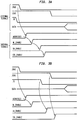
- FIGS. 3A and 3B are respectively timing diagrams for normal operation and test mode operation.
- the external control signals are the RAS (the row address strobe, active low), CAS , G , and data signals.
- the internal signals are addresses, WL_Enable (wordline enable), SA_Enable (sense amplifier enable), and Col_Enable (Column enable).
- the external strobe RAS initiates the generation of addresses which, in turn, generate the WL_Enable signal. After the timer 11 times out, the SA_Enable signal is generated, and after the timer 12 times out, the Col_Enable signal is generated.
- test mode signals TM_CSAE and TM_CCSLE
- TM_CSAE and TM_CCSLE Activating the test mode signals (TM_CSAE and TM_CCSLE) disable timers 11 and 12, causing the DRAM integrated circuit to be in test mode.
- the external strobe RAS initiates the generation of addresses which, in turn, generate the WL_Enable signal, as before, but this time the SA_Enable signal is not generated by the timer 11. Instead the SA_Enable signal is generated externally by the G signal passed by NAND gate 13. This SA_Enable signal, however, does not result in the generation of the Col_Enable signal; rather, the Col_Enable signal is generated by the CAS passed by NAND gate 16.
- the timing of internal signals Col_Enable and SA_Enable is controlled by external signal G and CAS , respectively, in test mode.
- the ability to control the timing of internal signals gives circuit designers essentially unlimited range of adjustments of timing delays to determine the actual delay time required in the design implementation.
- the circuit shown in Figure 1 or 2 has numerous applications.
- the circuit can be implemented in a DRAM to adjust the timing of the WL-SA Timing by providing for a different signal path upon activation of a test mode.
- the different signal path for example, causes the SA to be set with the falling edge of G and reset with the rising edge of G .
- test mode can be used to study, for example,:
- the invention can also be used to define a test mode which adjusts the SA-CSL timing, as depicted by the circuit of Figure 2. Invocation of this test mode is achieved by using the mode register to generate the TM_CCSLE signal.
- the SA-CSL timing can be adjusted using the CAS (Column Address Strobe) pin.
- G and CAS Column Address Strobe
- the use of separate external control signals ( G and CAS ) allows both WL-SA timing and SA-CSL timing to be independently adjusted in one row address strobe (RAS) cycle.
- Choosing the CAS pin instead of the G pin allows both WL-SA timing and SA-CSL timing to be independently adjusted in one row address strobe (RAS) cycle.
- a test mode for adjusting Column Address - DQ sensing timing (Query data from SA) can also be defined. Similarly, this timing can be controlled through the CAS pin. By adjusting the timing difference between addresses and the CAS edge, the column address - memory data query (DQ) sensing delay can be adjusted.
- DQ column address - memory data query
- a test mode for controlling the internal clock is also useful. For example, an extra pad is added to be used to provide internal timing. The purpose of the clock is controlled by the test modes. Since this clock pad is a non-functional pad, no conflict of purpose can occur, as with the CAS or G pins. If this extra pad is connected to a non-connect pin of a package, a test mode can be used to convert the non-connect pin to a general purpose clock pin for internal timing control.
- the invention can be used in either integrated circuit devices to control internal signals, such as to shift a local clock in a central processing unit (CPU) or adjust WL reset timer in a static RAM (SRAM) with self-reset.
- CPU central processing unit
- SRAM static RAM
Abstract
Description
Claims (21)
- A method for controlling timing of an internal control signal in an integrated circuit device using external control, the method comprising:providing first and second signal paths;generating a test mode signal that determines a mode of operation, the integrated circuit device being in the first mode of operation when the test mode signal is at a first signal level and being in the second mode of operation when the test mode signal is at a second signal level;
when the integrated circuit device is in the first mode of operation, the first signal path receives an internal signal and generates a first output signal in response to the internal signal, the first output signal being used to derive the timing of the internal control signal in the first mode of operation; and
when the integrated circuit device is in the second mode of operation, the second signal path receives an external signal provided at an external pin of the integrated circuit and generates a second output signal in response to the external signal, the second output signal being used to derive the timing of the internal control signal in the second mode of operation. - The method recited in claim 1 wherein the first circuit comprises a timing circuit generating the first output having a delay with respect to the internal signal.
- The method recited in claim 2 wherein the delay is predetermined by the timing circuit.
- The method recited in any preceding claim further comprising combining the first and second signal path with a select circuit and generating the internal control signal, the internal control signal being derived from the first output in the first mode of operation and derived from the second output in the second mode of operation.
- The method recited in any preceding claim wherein the first and second circuit responds to the test mode signal, the first circuit being enabled to activate the first signal path and the second circuit being disabled to deactivate the second signal path when the test mode signal is at the first signal level, and the first circuit being disabled to deactivate the first signal path and the second circuit being enabled to activate the second signal path when the test mode signal is at the second signal level.
- The method recited in claim 4 wherein said select circuit comprises a decoder for receiving the test mode signal and the first and second outputs, the decoder generating the internal control signal in response to the test mode signal, the internal control signal being derived from the first output when the test mode signal is at the first signal level and from the second output when the test mode signal is at the second signal level.
- The method recited in any preceding claim wherein the external pin is used or a different functional purpose during the first mode of operation and receives the external signal for deriving the timing of the internal signal during the second mode of operation.
- The method recited in any preceding claim wherein the integrated circuit comprises a random access memory (RAM) device, the internal signal is used to enable a wordline, and the internal control signal is used to enable a sense amplifier.
- The method recited in claim 8 wherein the external pin comprises a G pin of the RAM device.
- The method recited in any preceding claim wherein the integrated circuit comprises a RAM device, the internal signal is used to enable a sense amplifier and the internal control signal is used to enable a column.
- The method recited in claim 10 wherein the external pin comprises a CAS pin of the RAM device.
- A control circuit for controlling a timing of an internal control signal in an integrated circuit device using an external control, the circuit comprising:a first subcircuit receiving a test mode signal, the first subcircuit generating a first output in response to an internal signal when the test mode signal is at a first signal level;a second subcircuit receiving the test mode signal, the second subcircuit generating a second output in response to an external signal when the test mode signal is at a second signal level;and means for generating the test mode signal to determine the mode of operation.
- The control circuit recited in claim 12 wherein the first subcircuit comprises a timing circuit for generating the first output having a delay with respect to the internal control signal.
- The control circuit recited in claim 13 wherein the delay is predetermined by the timing circuit.
- The control circuit recited in one of claims 12-14 wherein the first and second subcircuit respond to the test mode signal, the test mode signal, when at the first signal level, enables the first subcircuit to permit the generation of the first output and disables the second subcircuit to prevent the generation of the second output, and when in the second signal level, disables the first subcircuit to prevent the generation of the first output and enables the second subcircuit to permit the generation of the second output.
- The control circuit recited in one of claims 12-15 further comprising a select circuit, the select circuit receives the first and second outputs and generates the internal control signal, the internal control signal being derived from the first output when the test mode signal is at the first signal level and from the second output when the test mode signal is at the second signal level.
- The control circuit recited in one of claims 12-16 wherein the external pin is used for a different functional purpose when the test mode is at the first signal level and at the second signal level.
- The control circuit recited in any of claims 12-17 wherein the intergrated circuit comprises a RAM device, the internal signal is used to enable a wordline, and the internal control signal is used to enable a sense amplifier.
- The control circuit recited in claim 18 wherein the external pin comprises a G pin of the RAM device.
- The control circuit recited in any of claims 12-19 wherein the integrated circuit comprises a RAM device, the internal signal is used to enable a sense amplifier, and the internal control signal is used to enable a column.
- The control circuit recited in claim 20 wherein the external pin comprises a CAS pin of the RAM device.
Applications Claiming Priority (2)
| Application Number | Priority Date | Filing Date | Title |
|---|---|---|---|
| US08/777,559 US5745430A (en) | 1996-12-30 | 1996-12-30 | Circuit and method to externally adjust internal circuit timing |
| US777559 | 2004-02-11 |
Publications (2)
| Publication Number | Publication Date |
|---|---|
| EP0851235A2 true EP0851235A2 (en) | 1998-07-01 |
| EP0851235A3 EP0851235A3 (en) | 1998-11-04 |
Family
ID=25110586
Family Applications (1)
| Application Number | Title | Priority Date | Filing Date |
|---|---|---|---|
| EP97310403A Withdrawn EP0851235A3 (en) | 1996-12-30 | 1997-12-22 | Circuit and method to externally adjust internal circuit timing |
Country Status (5)
| Country | Link |
|---|---|
| US (1) | US5745430A (en) |
| EP (1) | EP0851235A3 (en) |
| JP (1) | JPH10214133A (en) |
| KR (1) | KR19980064797A (en) |
| TW (1) | TW392266B (en) |
Families Citing this family (9)
| Publication number | Priority date | Publication date | Assignee | Title |
|---|---|---|---|---|
| US5903512A (en) * | 1996-12-30 | 1999-05-11 | Siemens Aktiengesellschaft | Circuit and method to externally adjust internal circuit timing |
| US6489819B1 (en) | 1998-10-27 | 2002-12-03 | Mitsubishi Denki Kabushiki Kaisha | Clock synchronous semiconductor memory device allowing testing by low speed tester |
| US6799290B1 (en) | 2000-02-25 | 2004-09-28 | Infineon Technologies North America Corp | Data path calibration and testing mode using a data bus for semiconductor memories |
| US6718487B1 (en) | 2000-06-27 | 2004-04-06 | Infineon Technologies North America Corp. | Method for high speed testing with low speed semiconductor test equipment |
| JP4263374B2 (en) | 2001-01-22 | 2009-05-13 | 株式会社ルネサステクノロジ | Semiconductor integrated circuit |
| US7751484B2 (en) * | 2005-04-27 | 2010-07-06 | Lsi Corporation | Method for composite video artifacts reduction |
| KR100932724B1 (en) * | 2005-09-09 | 2009-12-21 | 후지쯔 마이크로일렉트로닉스 가부시키가이샤 | Semiconductor integrated circuit |
| KR101912905B1 (en) * | 2012-08-16 | 2018-10-29 | 에스케이하이닉스 주식회사 | Cas latency setting circuit and semiconductor memory apparatus including the same |
| KR20160029378A (en) * | 2014-09-05 | 2016-03-15 | 에스케이하이닉스 주식회사 | Semiconductor Apparatus |
Citations (3)
| Publication number | Priority date | Publication date | Assignee | Title |
|---|---|---|---|---|
| US3633174A (en) * | 1970-04-14 | 1972-01-04 | Us Navy | Memory system having self-adjusting strobe timing |
| US5394403A (en) * | 1992-06-12 | 1995-02-28 | Sun Microsystems, Inc. | Fully testable chip having self-timed memory arrays |
| US5442642A (en) * | 1992-12-11 | 1995-08-15 | Micron Semiconductor, Inc. | Test signal generator on substrate to test |
Family Cites Families (3)
| Publication number | Priority date | Publication date | Assignee | Title |
|---|---|---|---|---|
| JPH04119600A (en) * | 1990-09-10 | 1992-04-21 | Mitsubishi Electric Corp | Dynamic random access memory device with built-in test mode function |
| US5627838A (en) * | 1993-09-30 | 1997-05-06 | Macronix International Co., Ltd. | Automatic test circuitry with non-volatile status write |
| JP3015661B2 (en) * | 1994-04-27 | 2000-03-06 | 株式会社東芝 | Non-volatile semiconductor memory |
-
1996
- 1996-12-30 US US08/777,559 patent/US5745430A/en not_active Expired - Lifetime
-
1997
- 1997-12-19 TW TW086119343A patent/TW392266B/en not_active IP Right Cessation
- 1997-12-22 EP EP97310403A patent/EP0851235A3/en not_active Withdrawn
- 1997-12-26 JP JP9360714A patent/JPH10214133A/en not_active Withdrawn
- 1997-12-30 KR KR1019970077844A patent/KR19980064797A/en not_active Application Discontinuation
Patent Citations (3)
| Publication number | Priority date | Publication date | Assignee | Title |
|---|---|---|---|---|
| US3633174A (en) * | 1970-04-14 | 1972-01-04 | Us Navy | Memory system having self-adjusting strobe timing |
| US5394403A (en) * | 1992-06-12 | 1995-02-28 | Sun Microsystems, Inc. | Fully testable chip having self-timed memory arrays |
| US5442642A (en) * | 1992-12-11 | 1995-08-15 | Micron Semiconductor, Inc. | Test signal generator on substrate to test |
Also Published As
| Publication number | Publication date |
|---|---|
| KR19980064797A (en) | 1998-10-07 |
| EP0851235A3 (en) | 1998-11-04 |
| TW392266B (en) | 2000-06-01 |
| JPH10214133A (en) | 1998-08-11 |
| US5745430A (en) | 1998-04-28 |
Similar Documents
| Publication | Publication Date | Title |
|---|---|---|
| US7855926B2 (en) | Semiconductor memory device having local sense amplifier with on/off control | |
| US5379261A (en) | Method and circuit for improved timing and noise margin in a DRAM | |
| US5903512A (en) | Circuit and method to externally adjust internal circuit timing | |
| US5623453A (en) | Synchronous semiconductor device with discontinued functions at power down | |
| US6154864A (en) | Read only memory embedded in a dynamic random access memory | |
| KR101138835B1 (en) | Semiconductor memory device | |
| KR100287184B1 (en) | Internal Clock Delay Circuit for Synchronous DRAM Semiconductor Device and Delay Method Thereof | |
| US5959915A (en) | Test method of integrated circuit devices by using a dual edge clock technique | |
| KR970023464A (en) | Semiconductor memory with test circuit | |
| EP0851235A2 (en) | Circuit and method to externally adjust internal circuit timing | |
| JP3406698B2 (en) | Semiconductor device | |
| US20040218438A1 (en) | Memory device with test mode for controlling of bitline sensing margin time | |
| KR100297708B1 (en) | Semiconductor memory device having clock synchronous precharge data I/O and precharge method using the same | |
| KR19990003680A (en) | Synchronous semiconductor memory device having a control unit for reducing the current consumption of the data input and output mask input buffer | |
| US7548478B2 (en) | Circuit and method for selecting test self-refresh period of semiconductor memory device | |
| KR100263256B1 (en) | Self cut-off type sense amplifier operable over a wide range of power supply voltage | |
| US6992949B2 (en) | Method and circuit for controlling generation of column selection line signal | |
| US7167948B2 (en) | Semiconductor memory device | |
| US6243312B1 (en) | Semiconductor memory device | |
| KR20000008778A (en) | Row address strobe access time control circuit | |
| US5202888A (en) | Semiconductor memory device having a multibit parallel test function and a method of testing the same | |
| US6876564B2 (en) | Integrated circuit device and method for applying different types of signals to internal circuit via one pin | |
| US6553520B1 (en) | Integrated circuit devices with mode-selective external signal routing capabilities and methods of operation therefor | |
| KR100191022B1 (en) | Integrated semiconductor circuit device | |
| KR100219494B1 (en) | Semiconductor memory apparatus for controlling special mode |
Legal Events
| Date | Code | Title | Description |
|---|---|---|---|
| PUAI | Public reference made under article 153(3) epc to a published international application that has entered the european phase |
Free format text: ORIGINAL CODE: 0009012 |
|
| AK | Designated contracting states |
Kind code of ref document: A2 Designated state(s): DE FR GB IE IT NL |
|
| AX | Request for extension of the european patent |
Free format text: AL;LT;LV;MK;RO;SI |
|
| PUAL | Search report despatched |
Free format text: ORIGINAL CODE: 0009013 |
|
| AK | Designated contracting states |
Kind code of ref document: A3 Designated state(s): AT BE CH DE DK ES FI FR GB GR IE IT LI LU MC NL PT SE |
|
| AX | Request for extension of the european patent |
Free format text: AL;LT;LV;MK;RO;SI |
|
| 17P | Request for examination filed |
Effective date: 19990428 |
|
| AKX | Designation fees paid |
Free format text: DE FR GB IE IT NL |
|
| 17Q | First examination report despatched |
Effective date: 20040202 |
|
| STAA | Information on the status of an ep patent application or granted ep patent |
Free format text: STATUS: THE APPLICATION IS DEEMED TO BE WITHDRAWN |
|
| 18D | Application deemed to be withdrawn |
Effective date: 20040615 |
|
| REG | Reference to a national code |
Ref country code: HK Ref legal event code: WD Ref document number: 1015031 Country of ref document: HK |