This patent application claims a conventional priority based
on a Japanese patent application, HEI9-011960 filed on January 7,
1997, the contents of which are incorporated hereinto by reference.
BACKGROUND OF THE INFVENTION
1. Field of Invention
The present invention relates to an initial synchronization
method and a receiver for initial synchronization in a DS-CDMA
(Direct Sequence-Code Division Multiple Access) inter base station
asynchronous cellular system.
2. Description of Related Art
CDMA cellular systems based on code division multiple access
(CDMA) using a direct sequence (DS)-type spread spectrum (SS)
greatly increases the channel capacity. These systems are
receiving much attention in the recent work on ground mobile
communication. In general, the frequency utilization efficiency
of a CDMA system is inferior to that of other multiple access
systems (FDMA, TDMA) because of mutual interference with other
stations. However, the cellular system is robust against
interference since the spatial frequency re-utilization efficiency
(repetition rate of cells having the same frequency) contributes
to the efficiency of the overall frequency utilization. Hence, a
CDMA cellular system having a high cell repetition rate is assured
to be an effective system in the future.
Generally, cellular systems require two kinds of cell
searches, namely, an initial cell search by which an initial cell
to be connected to a mobile station is identified, and a
neighboring cell search by which neighboring cells are searched
for the hand-over. Notably in DS-CDMA cellular systems, each of
the cells uses the same frequency. Hence, the initial
synchronization needs to reduce the timing error between the
spread code of the received signal and the spread code replica
generated by the receiver to within ½ chip period while the
simultaneous cell search.
DS-CDMA cellular systems can be categorized into two classes,
namely, inter base station synchronous systems in which temporal
synchronization is performed strictly among all base stations, and
inter base station asynchronous systems in which temporal
synchronization is not performed. Inter base station synchronous
systems achieve inter base station synchronization using other
systems such as the GPS (Global Positioning System) . Since each
of the base stations uses the same long code by giving it a delay
which differs from one base station to another, it suffices to
synchronize only the timing of the long code during the initial
search. In addition, the neighboring cell search for the hand-over
can be performed at a higher speed since the mobile station
receives the code delay information of the neighboring base
stations directly from the given base station with which the
mobile station is at a given time communicating.
On the other hand, in inter base station asynchronous systems,
each of the base stations uses a different spread code in order to
identify the base stations. The mobile station needs to identify
the spread codes in performing the initial cell search. When
searching neighboring cells for the hand-over, the number of codes
to be searched can be limited by obtaining the spread codes of the
neighboring base stations from the current base station to which
the mobile station belongs. However, in comparison with inter
base station synchronous system, the search time is longer.
Indeed when a long code is used for the spread code, the amount of
time for the cell search becomes enormous. However, this inter
base station asynchronous system has an advantage in that other
systems such as GPS are not needed.
A cell search system capable of solving these problems
inherent in the inter base station asynchronous systems and
performing initial synchronization at a high speed is being
proposed by Kenichi Higuchi, Mamoru Sawahashi, and Fumiyuki Adachi,
in "Two-step high speed long code initial synchronization method in
the DS-CDMA inter base station asynchronous system" (Shingakugihou
CS-96-19, RCS96-12 (1996-05)) . According to this initial
synchronization method, a spread code sequence synthesized from a
long code corresponding to the cells and a short code
corresponding to a communication channel is used to doubly spread
the data. A second short code common to all cells is assigned to
the control channel in order to perform the initial
synchronization in two steps.
More specifically only the short code is used and the long
spread code is masked for the control channel transmitted from the
base station of every cell. On the mobile station side, at the
first stage, a matched filter de-spreads the received signal by
using the short code and detects the timing of the long code. At
the second stage, a correlator identifies the long code
corresponding to a cell by using a spread code sequence
synthesized from the long code corresponding to the cell and the
specific short code.
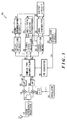
Fig. 1 illustrates a configuration of cells. In Fig. 1, the
numeral 61 represents the mobile station. Each of the
cells #1
through #n has one of the base stations BS
1, BS
2,
, BSn,
respectively. Each base station sends a signal to the
mobile
station 61 by using symbols which are doubly spread by the
long
codes #1, #2,
, #n and the short codes #0 - #s identifying each
channel. Here, the short codes #0 - #s are common to each of the
cells. In addition, the common
short code #0 is assigned to the
control channel of each of the cells.
Fig. 2 is a timing chart for explaining the conventional two-step
high speed initial synchronization method, and an example of
a signal of a control channel received at a mobile station. The
control channel received from each of the base stations contains
certain symbols, which have been spread only by the short code #0
every long-code period. Signals received from BSk-2, BSk-1, and BSk
are shown in the drawing and the certain symbols are shown as
shaded portions of the signals. This short code #0 is assigned
commonly to all of the base stations, and this is achieved by not
spreading the signals with the long codes over a certain period.
The other symbol positions of the control channels are doubly
spread using the long code #i, which differs from one base station
to another, and the short code #0. In this way, the control
channels transmitted from each of the base stations BSk-2 - BSk are
asynchronously multiplexed and are received at the mobile station.
In the first stage, the mobile station finds a correlation
between the base band received signal and the short code #0 using
a matched filter. The peak of the correlation is detected at the
temporal position corresponding to the reception timing of the
symbol which is spread with the short code #0 of the control
channel of the base stations. The timing corresponding to the
maximum electric power is detected after these peak electric
powers have been detected over the R-period of the long code. The
detected timing, the code timing T, is determined to be the long
code synchronization timing transmitted from the base station of
the new cell in which a mobile station is located.
In the second stage, in order to identify the base station BSk,
the mobile station 61 identifies the long code #k that is used to
spread the control channel, the long code timing T of which has
been detected. In order to accomplish this, the long code #k is
sequentially selected out of the long codes #1 - #n of the system
in the initial cell search. A replica code is synthesized from
the selected long code #k and the short code #0, and correlation
is detected by a correlator using the long code synchronization
timing obtained in the first stage.
The correlation detection is continued over the range of long
codes #1 - #n until a long code causes the correlation detection
value to exceed the threshold value. The long code that has
exceeded the threshold value is judged to be the long code #k of
the new base station, and the cell search is completed.
When searching the neighboring cell for the hand over,
similarly, a replica code is synthesized from the short code #0
and the long code #k. The long code #k is sequentially selected
from the long codes of neighboring cells transmitted by the
current base station to the mobile station. Correlation is
detected using the long code synchronization timing.
As seen in the above, cell search can be performed at a high
speed by performing the timing synchronization and the
identification of the long code separately. According to the
standard inter base station asynchronous cellular systems,
correlation detection needs to be performed approximately (the
number of spread codes × the number of phases of the spread codes)
times to search a cell.
On the other hand, according to this method, it suffices to
perform correlation detection (the number of spread codes + the
number of phases of the spread codes) times. Therefore, in
comparison with the standard inter base station asynchronous
cellular systems, a cell can be searched at a high speed. However,
a problem still remains when the correlation detection is
performed using a correlator, as is done in the prior art. The
length of time required for detecting every correlation still
remains long. Hence, it is desired that the initial
synchronization be performed at a higher speed.
SUMMARY OF THE INVENTION
Therefore, it is an object of the present invention to
provide an initial synchronization method and a receiver for a DS-CDMA
inter base station asynchronous cellular system capable of
performing cell searches at a higher speed.
In order to achieve the above object, according to the first
aspect of the present invention, spread code sequences are made of
long codes corresponding to the cells and short codes
corresponding to the communication channels. A specific short
code common to each of the cells is assigned to the control
channel for the initial synchronization of the DS-CDMA inter base
station asynchronous cellular system.
Based on the correlation between the specific short code and
the received signal, the long code synchronization timing
transmitted from the corresponding base station is determined. A
synthesized code for each long code is defined by a combination of
the long code and the specific short code. The matched filter
detects the correlation between the received signal and each of
several segments, each segment being taken from a portion of one
of the synthesized code. In particular, the segment taken from a
next synthesized code is extracted starting from a position in the
next synthesized code, which is shifted by a predetermined amount
from where the segment of the first synthesized code was extracted.
The amount of shifting, however, is smaller than the length of the
segments. The long code transmitted from the corresponding base
station is identified based on the magnitude of the electric power
of the correlation.
The correlation between each of the segments and the received
signal is detected based on the long code synchronization timing,
by sequentially replacing each of the segments every time, an
interval of the received signal corresponding to the prescribed
chip number is newly input to the matched filter.
A portion of the base band received signal still remains in
the matched filter at the time the correlation with the segment of
one synthesized code has been processed. Thus, the portion can be
used for processing the correlation with the segment of the next
synthesized code instead of being disposed of. Consequently, the
long codes can be searched at a higher speed. In contrast, when a
sliding correlator is used as in the prior art, the received
signal used for the previous correlation is discarded immediately
before processing the next correlation.
According to the second aspect of the present invention, the
receiver for the DS-CDMA inter base station asynchronous cellular
system uses spread code sequences synthesized from long codes
corresponding to the cells and short codes corresponding to the
communication channels. A specific short code is assigned to the
control channel of all cells. The receiver has a spread code
generating means for outputting each of several segments, each
segment being taken from a portion of one of the synthesized code.
In particular, the segment taken from a next synthesized code
is extracted starting from a position in the next synthesized code,
which is shifted by a predetermined amount from where the segment
of the first synthesized code was extracted. The amount of
shifting, however, is smaller than the length of the segments. A
matched filter finds a correlation between the output of the
corresponding spread code generating means and the received signal.
A long code synchronization timing determination means determines
the long code synchronization timing transmitted from the
corresponding base station using the correlation between the
specific short code and the received signal.
The long code identification means supplies one of the
segments to the matched filter from the spread code generating
means based on the long code synchronization timing. Then the
long code identification means sequentially replaces each of the
segments and supplies the segment every time an interval of the
received signal corresponding to the amount of shifting is newly
input to the matched filter, and identifies the long codes
transmitted from the corresponding base station based on the
magnitude of the electric power of the output signal of the
matched filter. Accordingly, long codes can be searched faster.
According to the third aspect of the present invention, the
spread code generating means further outputs the specific short
code. The long code synchronization timing determination means
supplies the specific short code from the spread code generating
means to the matched filter, and determines the synchronization
timing of the long code transmitted from the corresponding base
station based on the electric power of the output signal of the
matched filter. Therefore, the long code synchronization timing
can be easily determined. The long code synchronization timing
and the identification of the long code can be determined using
the matched filter.
According to the fourth aspect of the present invention, the
matched filter has multiple sample holders and multiple
multipliers for outputting signals from the sample holders as the
first and second outputs according to the value of the bits
corresponding to the output of the spread code generating means.
A first analog addition circuit adds the first outputs of the
multipliers. A second analog addition circuit adds the second
outputs of the multipliers. A third analog addition circuit
subtracts the output of the first analog addition circuit from the
output of the second analog addition circuit. Since the above-mentioned
matched filter consumes a small amount of electric power,
the electric power consumption of the receiver can be reduced
accordingly.
BRIEF DESCRIPTION OF THE DRAWINGS
Fig. 1 shows a conventional structure of the cells of DS-CDMA
communication system.
Fig. 2 is a timing chart of the conventional two-step high
speed initial synchronization method.
Fig. 3 is a block diagram of the signal reception circuit of
the mobile station 61 shown in Fig. 1.
Fig. 4 is a block diagram of the long code search circuit
shown in Fig. 3.
Fig. 5 is a block diagram of the matched filter 18.
Fig. 6 shows a synthesized code to be input to the
coefficient input terminal of the matched filter.
Fig. 7 is a flowchart of the initial cell search of the
embodiment shown in Fig. 4.
Fig. 8 shows the relation between the base band received
signal and the segments of the synthesized codes to be
correlation-processed according to the embodiment of the present
invention.
Fig. 9 shows the relation between the base band received
signal and the segments of the codes according to the prior art.
Fig. 10 is a block diagram of an example of the matched
filter in Fig. 1.
Fig. 11 illustrates the inversion amplifier Amp.
Fig. 12 illustrates the multiplier MUX.
Fig. 13 illustrates the reference voltage generator Vref.
Fig. 14 illustrates an analog operation circuit that supplies
the input voltage to the inversion amplifier via capacitors.
DETAILED DESCRIPTION OF THE INVENTION
The preferred embodiment of the present invention will be
explained with reference to the attached drawings. Each base
station periodically masks the long code of one information symbol
length every long code cycle which starts at a prescribed time of
the control channel, and transmits the symbol that has been spread
only by the short code #0 that is common to all base stations.
The transmitter of the base station BS transmits a transmission
signal obtained by spreading the transmission data with binary
spread codes and QPSK-modulating the transmission signal.
Fig. 3 is a block diagram of the signal reception circuit of
the mobile station 61 shown in Fig. 1. In this drawing, a
spectrum spread signal received by a reception antenna 11 is
demodulated from the BPSK and transformed into an intermediate
frequency signal by a high frequency receiver 12, split into two
signals by a distributor 13, and supplied to multipliers 16 and 17.
An oscillator 14 generates a signal (cos ωt) having an
intermediate frequency. The output from the oscillator 14 is
directly supplied to the multiplier 16. The output from the
oscillator 14 is also input to the multiplier 17 via a phase shift
circuit 15 which shifts the phase of the output signal supplied
from the oscillator 14 by π/2.
The multiplier 16 multiplies the intermediate frequency
signal received from the distributor 13 by the oscillation output
received from the oscillator 14 and outputs a base band signal Ri
which is an in-phase component (I component) and is output via a
low-pass filter 62. The multiplier 17 multiplies the intermediate
frequency signal received from the distributor 13 by the output
(sinωt) of the phase shift circuit 15, and outputs a base band
signal Rq which is a quadrature component (Q component). In this
way, the received signal is quadrature-detected.
The base band signals Ri and Rq are input to a complex-type
matched filter 18, multiplied by a PN code sequence generated by a
PN code sequence generator 19, and are de-spread. The in-phase
component Si of the de-spread output and the quadrature component
Sq of the de-spread output received from the complex-type matched
filter 18 are input to a delay detection circuit 20, a signal
level detector 22, and a phase correction means 24. The delay
detection circuit 20 detects the delay of the de-spread output Si
and Sq and outputs the detected delay to a frame synchronization
circuit 21 which detects the timing of each frame. The resultant
output timing signal Ct is input to a phase correction means 24.
The signal level detector 22 calculates the electric power
(correlation value) from the de-spread output Si which is the I
component and the de-spread output Sq which is the Q component.
The resultant output Lb from the signal level detector 22 is
supplied to a multi-path selector 23 and a long code search
circuit 27. The long code search circuit 27 searches the long
code and supplies the number Lc of the long code to the PN
generator 19.
The multi-path selector 23 selects multiple peaks having high
received signal levels from among the peaks of the signals
received through multiple paths. The output Cm of the multi-path
selection circuit 23 is input to the phase correction means 24.
The phase correction means 24 corrects the phase of the signal
received through each path. The Rake synthesizer 25 synthesizes,
at a synchronized timing, the phase-corrected output of each path
received from the phase correction means 24, and outputs the
synthesized output to the output circuit 26. The output of the
output circuit 26 is supplied to a subsequent decision circuit or
the like not shown in the drawing, which de-modulates and
processes the signal.
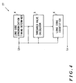
Fig. 4 is a block diagram of the long code search circuit 27
shown in Fig. 3. The electric power Lb output from the signal
level detector 22 is supplied to the long code synchronization
timing determiner 4, the threshold value calculator 5, and the
long code identifier 6.
The PN generator 19 is controlled by the long code
synchronization timing determiner 4 and the long code identifier 6.
At the time of the initial search, the PN generator 19 outputs the
short code #0 that is common to the control channels of all base
stations. After the long code synchronization timing has been
determined, each segment having N chips, which is a portion of the
spread code sequence synthesized from the short code #0 and one of
the long codes #i unique to each base station, is sequentially
loaded and output.
In the neighborhood search before the hand-over, as in the
initial cell search, the short code #0 common to the control
channels of all base stations is output. After the long code
synchronization timing of the base station to be handed over to is
determined, the long code search circuit 27 sequentially replaces
and outputs each segment having N chips, which forms a portion of
a code synthesized from the short code #0 and one of the long
codes #i. In particular, the segment taken from a next
synthesized code is extracted starting from a position in the next
synthesized code which is shifted by a predetermined amount from
where the segment of the first synthesized code was extracted.
The amount of shifting, however, is smaller than the length of the
segments. The long code search circuit 27 searches the long code
of the new base station based on the information of the long codes
of the neighboring cells received from the control channel of the
base station to which the mobile station currently belongs.
The long code
synchronization timing determiner 4, in the
initial cell search,
The
threshold value calculator 5 calculates a threshold value
to be output to the
long code identifier 6 based on the electric
power of the maximum correlation value of the long code
identification timing.
In the neighboring cell search before the hand-over,
The long code identifier 6 sequentially supplies and replaces
each of the segments after the long code identification timing is
detected, and compares the output Lb of the signal level detector
22 with the prescribed threshold value. If the output Lb of the
signal level detector 22 exceeds this threshold value, the
synthesized code supplied to the matched filter is identified as
the synthesized code of the new base station. The long code of
the identified synthesized code, which has been supplied to the PN
code generator 19, is identified as the long code of the new base
station.
Fig. 5 is a schematic drawing of the matched filter 18. In
this drawing, it is assumed that the base band received signal is
input with positive and negative polarities and that the segments
of each synthesized code consists of a binary code sequence, which
has values 1 and/or - 1.
As shown in Fig. 5, the complex-type matched filter 18 has a
shift register 71 consisting of steps, the number of which equals
a chip number associated with the amount of shifting between
successive synthesized codes, a multiplier 72 for multiplying the
tap output of each of the register steps and the coefficient
inputs, and an adder 73 for adding all the outputs of the
multiplier 72. A portion of the shift register 71 consists of, in
practice, analog devices such as a CCD (Charge Coupled Device) and
a SAW (Surface Acoustic Wave) filter, or digital devices such as
digital IC circuits. As an alternative, a little electric matched
filter having analog operation circuits can be used to save the
power consumption.
In any of these cases, the complex-type matched filter 18 is
operated only for the duration of time in which the peaks of the
correlation value can be detected at prescribed time intervals.
Even if a matched filter consumes a lot of electric power in the
operation for the synchronization, the matched filter operates
only at intervals and so the electric power consumption, as a
whole, can be kept low.
Fig. 6 shows segments of the synthesized codes to be input to
the coefficient input terminals of the matched
filter 18. The
symbols A, B,
, Z written above the code sequences indicate that
respective codes are input to the coefficient input terminals A, B
- Z, respectively, of Fig. 5. The symbol M represents a natural
number.
Fig. 7 is a flow chart for explaining the initial cell search
operation. In S21, the PN generator 19 loads the short code #0 to
the complex-type matched filter 18. In S22, a correlation between
the base band received signal and the short code #0 is obtained by
the complex-type matched filter 18. The signal level detector 22
detects the electric power of the output of the complex-type
matched filter 18, and outputs the result to the long code
synchronization timing determiner 4.
In S23, the long code synchronization timing determiner 4
stores the values of this electric power, and their time within
the period of the long code, when the electric power exceeds a
certain threshold value. As an alternative, the threshold value
can be adaptive-controlled corresponding to the base band received
signal by determining the average level of the electric power that
has been output from the signal level detector 22.
The above-mentioned process is performed over multiple
periods of the long code and the values and their time are stored
for multiple times. The stored values of the corresponding time
are averaged and are compared with those of the different time.
The timing at which the electric power corresponding to the
maximum correlation value is achieved is selected after the
averaging operation has been completed. The selected timing is
output to the PN generator 19 as the long code synchronization
timing.
In S24, the long code
synchronization timing determiner 4
initially sets the value of i to 1. In S25, the
PN generator 19
loads a segment having a prescribed chip length, for example, 128
chips, which forms a portion of a code synthesized from the
long
code #1 and the
short code #0. As shown in Fig. 6, PN(1)
128 ,
PN(1)
127, , PN(1)
1 are initially input to the coefficient input
terminals A - Z.
In S26, the complex-type matched filter 18 finds a
correlation between the base band received signal and the segment
of the synthesized code #1, namely, a partial correlation with the
synthesized code #1. The long code identifier 6 determines
whether the electric power of the correlation output has exceeded
the threshold value or not. Specifically, a correlation between
the base band received signal and the segment of the synthesized
code #1 is obtained. If the output of the signal level detector
22 is greater than the prescribed threshold value calculated by
the threshold value calculator 5, then the process is advanced to
S27. If the output of the signal level detector 22 is not greater
than the prescribed threshold value calculated by the threshold
value calculator 5, the process is advanced to S28.
The threshold value calculator 5 can adaptively control the
threshold value corresponding to the base band received signal by
outputting an electric power level which represents a prescribed
percentage of the electric power corresponding to the maximum
correlation peak value at the time of the long code
synchronization timing or the average level of the output electric
power of the signal level detector 22 up to the present time.
In S27, the long code #i obtained at this stage is determined
to be the long code for the desired base station, and the cell
search is finished. In S28, it is determined whether the long
code #i is the last long code or not. If the long code #i is the
last long code, then the process is returned to S21, and the
process is repeated beginning from the determination of the long
code synchronization timing. If the long code #i is not the last
long code, the process is advanced to S29. The last long code
used in this DS-CDMA inter base station asynchronous cellular
system is labeled as, for example, long code #512.
In S29, the value of the synthesized code #i is incremented
by one. For example, if i = 1, it is set to i = 2, and the
process is returned to S25. In S25, the PN generator 19 loads a
segment of the synthesized code #2 synthesized from the long code
#2 and the short code #0 to the complex-type matched filter 18.
It suffices to regard this segment of the synthesized
code #2
as a sequence PN(2)
128, PN(2)
127,
, PN(2)
1, as in the case of the
synthesized
code #1, and obtain a correlation with the base band
received signal. However, in order to determine the correlation
peak of the electric power, a certain amount of processing time,
changes in the peak phase and the like must be taken into
consideration. Therefore, the base band received signal is
correlated with the segment of the next synthesized
code #2, after
the correlation between the base band received signal and the
segment of the synthesized
code #1 is obtain, and when the M chips
of the base band received signal have been input. While the above
procedure is being performed, the M chips of the base band
received signal are newly being input to the
shift register 71
shown in Fig. 5 and are being shifted.
Therefore, the segment of the next synthesized
code #2 with
which the correlation is obtained needs to be put in
correspondence with the shift of the base band received signal.
Hence, as shown in Fig. 6, the segment is input to the coefficient
input terminals A - Z shown in Fig. 5 as a sequence PN(2)
M + 128 ,
PN(2)
M + 127, , PN(2)
M + 1.
In the following steps S26 - S29, the same process performed
for the segment of the synthesized code #1 is repeated for the
segment of the synthesized code #2. Theoretically, the value of M
can be set to M = 1. However, when the accuracy of the chip
synchronization, variations of the correlation peak and the like
are taken into consideration, setting M = 4, by which the margin
of such errors can be accommodated, is appropriate. The value of
M may be set low in comparison with the chip number of the short
code.
A similar process will be explained in the following. When a
partial correlation is obtained in S25 by loading the segment of
the synthesized
code #512 corresponding to the last
long code #512,
this segment is represented by the sequence PN(512)
511M+ 128 ,
PN(512)
511 M + 127, , PN(512)
511M + 1 as shown in Fig. 6. These
segments of the synthesized code #i can be generated every time.
However, they can also be pre-synthesized, stored in a memory
inside the
long code identifier 6, taken out and read as necessity
arises.
Fig. 8 shows the correspondence between the base band
received signal and the segment of each synthesized code to be
correlation-processed with the base band received signal. In the
complex-type matched filter 18, the base band received signal is
correlated with a segment consisting of the first through 128-th
chips of the synthesized code #1 at the long code synchronization
timing. Here, the oldest chip of the base band received signal is
determined to be the first chip. With reference to this first
chip, the positions of the chips of the base band received signal
are shown. In the drawing, the positions of the chips of the base
band received signal are indicated in parentheses.
M chips of the base band received signal are newly input and
shifted M times. This time, the M + 1 th through M + 128th chips
of the base band received signal are correlated with the segment
consisting of the M + 1 th through M + 128th chips of the
synthesized code #2. Next, M further chips of the base band
received signal are input and shifted M times. This time, the 2M
+ 1 th through 2M + 128th chips of the base band received signal
are correlated with the segment consisting of the 2M + 1 th
through 2M + 128th chips of the synthesized code #3.
The complex type matched filter 18 continues to perform a
similar correlation process. When the segment of the last
synthesized code #512 is correlated with the base band received
signal, the 511M + 1 th through 511M + 128th chips of the base
band received signal are correlated with the segment consisting of
the 512M + 1 th through 511M + 128th chips of the synthesized code
#512.
As explained in the above, the segment of each synthesized
code #i is obtained by shifting the cut out interval by the
prescribed M chips corresponding to the new input of the base band
received signal to be correlated with. The detection of the
correlation between each of the segments and the base band
received signal is initiated by the long code identification
timing. Each of the segments is sequentially replaced whenever M
chips of the base band received signal are newly input to the
complex-type matched filter 18 and a new correlation detection is
performed.
The initial cell search can be performed at a high speed by
the above process. For example, if the chip number N of the
segment is 128 (one symbol), the value of M is 4, the total number
of the long codes is 512, and all the long codes can be searched
once within at most the time corresponding to 128 + (512 - 1) × 4 =
2172 chips.
Fig. 9 shows the relationships between the base band received
signal and the synthesized signal to be correlation-processed with
the base band received signal. This figure illustrates the
conventional art, which uses the same correlator as that explained
in the prior art reference cited in the "Description of Related
Art". The segment for identifying the long code has symbols of
128 chips, the same as the present embodiment.
At the time specified by the long code synchronization timing,
the first through 128th chips of the base band received signal are
correlated with the first through 128th chips of the segment of
the synthesized code #1. Then, the 128 + 1 th through 128 × 2 th
chips of the base band received signal are correlated with the 128
+ 1 th through 128 × 2 th chips of the segment of the synthesized
code #2. Next, the 128 × 2 + 1 th through 128 × 3 th chips of the
base band received signal are correlated with the 128 × 2 + 1 th
through 128 × 3 th chips of the segment of the synthesized code #3.
When a correlator of the prior art is used, at the time at
which the correlation between the base band received signal and
one of the synthesized codes has just been processed, the base
band received signal no longer remains. On the other hand,
according to the embodiment of the present invention, a portion of
the base band received signal still remains inside the matched
filter at the time at which the correlation between the base band
received signal and one of the synthesized codes has been
processed. Therefore, the remaining portion of the base band
received signal can be used for the correlation processing with
the segment of the next synthesized code. Consequently, according
to the embodiment of the present invention in which a matched
filter is used, the search speed is improved by N/M times. In the
case where N = 128 and M = 4, the search speed is improved by
128/4 = 32 times.
When searching the neighboring cells before the hand-over,
the long codes exceeding the threshold value can be searched in
the same way as the initial cell is searched, that is, by
sequentially inputting the segment of a code, which is synthesized
from the long code to be searched and the short code #0, to the
matched filter. The long code is input based on the information
on the long codes of the neighboring cells supplied from the
control channel after the long code synchronization timing has
been determined. The search speed is similarly improved by N/M =
128/4 = 32 times in comparison with the conventional art.
In the above explanation, only one matched filter is used.
However, the search speed can be further improved by using
multiple matched filters, for example two, and by simultaneously
performing the correlation detection of different long codes in
parallel .
According to this embodiment of the present invention, the
base band received signal is corrected with the segment of only
one synthesized code at a time. However, if the detected long
code synchronization timing is displaced from the true long code
synchronization timing due to the multi-paths or the like, the
segment of the synthesized code would be correlated with the base
band received signal at a time displaced from the true long code
synchronization timing. In such a case, it may be impossible to
identify the long codes.
Therefore, the base band received signal is correlated with
the same synthesized code multiple times by displacing the
relative timing within several chips at a time. The time at which
the maximum correlation electric power has been obtained from
among the electric power values obtained from these multiple
correlation processing operations is selected as the true long
code synchronization timing. Moreover, the desired long codes can
be identified from the code numbers of the synthesized codes used
in these multiple correlation processing operations.
A concrete explanation will be given with reference to Fig. 7
again. In S26, after the base band received signal and the
segment of one of the synthesized codes are correlated at the long
code synchronization timing, even while the base band received
signal is being input to the complex-type matched
filter 18,
The preserved maximum electric power value is compared with
the predetermined threshold value calculated by the threshold
value calculator 5. If the preserved maximum electric power value
exceeds this threshold value, the process is advanced to S27.
Otherwise, the process is advanced to S28.
When the process is returned to S26 via S28, S29 and S25, the
correlation between the base band received signal and the segment
of the next synthesized code is detected. However, as mentioned
in the above, this step is performed after the M chips of the base
band received signal have been newly input to the complex-type
matched filter 18. Hence, the number of electric power values of
the output of the signal level detector 22 to be stored
continuously can be arbitrarily set as long as it is less than or
equal to M. Conversely, the value of M can be determined
corresponding to the chip number to be stored continuously.
Fig. 10 illustrates an example of the complex-type matched
filter 18 shown in Fig. 4. Since the electric power consumption
of the matched filter is small, the electric power consumption of
the mobile station to which the present invention is applied can
be further reduced.
In order to simplify the drawings, the spread code sequences
illustrated therein consist of 6 bits and have six delay stages.
However, since far longer code sequences are used for the actual
spread code sequences in practice, the number of stages actually
installed in the matched filter 18 corresponds to the actual
spread code sequences.
Each of the base band received signals Si and Sq is
distributed and sequentially input to one of the sample holders
31-1 - 31-6 by the controller 32 which controls the sampling
timing. Each of the outputs of the sample holders 31-1 - 31-6 is
multiplied in the multipliers 33-1 - 33-6 by the output of the
spread code generator 35, which generates spread code sequences,
and added is then in the adders, 36 - 41, and the correlation
values Vr are output. The reference voltage is input to the
multipliers 33-1 - 33-6 from the reference voltage generator 34.
Each of the sample holders 31-1 - 31-6 have an analog switch
controlled by the controller 32, a capacitor C1, and an inversion
amplifier Amp. Each of the adders 36 - 41 has capacitors
connected to multiple input terminals and an inversion amplifier
Amp. In this matched filter 18, the capacitors are connected
between the input sides and the analog operation circuits (neuro-operation
amplifier) in the sample holders 31-1 - 31-6 and the
adders 36 - 41.
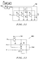
Fig. 11 is the inversion amplifier Amp shown in Fig. 10 (a).
The switch 51 is serially connected between the power source Vdd
and the inversion amplifier Amp. A power controller 58 controls
the switch 51 so as to activate the inversion amplifier Amp only
when necessary. The CMOS inverters 52 - 54 are cascade-connected.
The input terminal Vi is the input of the CMOS inverter 52, and
the output terminal Vo is the output of the CMOS inverter 54.
Installed between the two terminals is the capacitance Cf for
feedback.
The inversion amplifier Amp uses the inverters as amplifiers
through which the outputs of the CMOS inverters shift from a high
level to a low level or from a low level to a high level. The
inversion amplifier Amp has an odd number stages of CMOS inverters,
for example, three stages of CMOS inverters as shown in the
drawing. The resistors R1 and R2 divide the electric power source
voltage between the stages of the CMOS inverters 53 and so control
the gain of the amplifier Amp. The capacitor Cg is installed
between the output terminal Vo and the earth for phase adjustment.
The resistors R1 and R2 and the capacitor Cg prevent oscillation
of the inversion amplifier Amp.
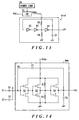
Fig. 14 shows the analog operation circuit that supplies the
input voltages via capacitors. The input voltages V1 and V2 are
supplied to the inversion amplifier Amp via capacitors C1 and C2,
respectively. Since the voltage amplification factor of the
inversion amplifier Amp is very large, the voltage value Vb at
point B, the input side of this inversion amplifier, is kept
almost constant. Point B is connected to the gate of a transistor,
which constitutes the CMOS inverter 52, and to the capacitors C1,
C2 and Cf. Point B is in a floating state with respect to any
electric power sources.
Therefore, if the electric charge stored in each of the
capacitors C1, C2 and Cf is zero in the initial state, the total
amount of electric charge stored in these capacitors remains zero,
even when the input voltages V1 and V2 are supplied. This
observation can be expressed in terms of the formula of electric
charge conservation:
C1(V1-Vb) + C2(V2-Vb) + Cf(Vout-Vb) = 0
Here, the symbols C1, C2, and Cf represent the capacitance of
the capacitors C1, C2, and Cf. Each of the input voltages V1 and
V2 is replaced by the voltage measured with respect to the
reference voltage Vb at point B as follows.
V(1) = V1-Vb, V(2) = V2-Vb, V'out = Vout-Vb
Then the following equation can be derived.
V'out = - {(C1/Cf)V(1) + (C2/Cf)V(2)}
In other words, the output voltage Vo is obtained by
inverting the polarity of the sum of the input voltages V(i)
measured with respect to Vb multiplied by the coefficient (Ci/Cf)
which represents the ratio of the input capacitance Ci with
respect to the feedback capacitance Cf. The output voltage V' is
output from the analog operation circuit (neuro-operation
amplifier).
The sample holders 31-1 - 31-6 are the particular type of the
analog operation circuits (neuro-operation amplifiers) shown in
Fig. 14, which has only one input terminal. If the values of the
input capacitance C1 and the feedback capacitance Cf are equal,
the output voltage becomes - V(1) in accordance with the equation
(3). In other words, the voltage of the base band received signal
is inverted and output when the controller 32 opens the input
switch.
The controller 32 controls the sample holders 31-1 - 31-6 by
sequentially supplying control signals to the sample holders 31-1
- 31-6. Each of the control signals close and sequentially opens
the analog switch installed in each of the sample holders 31-1 -
31-6, at the timing of each of the chips of the spread modulation
signal, to take in the input voltage. In this way, the received
signal corresponding to one period of the spread code sequence is
taken in by each of the sample holders 31-1 - 31-6, the polarity
of the received signal is inverted, and the received signal is
output. The outputs of the sample holders 31-1 - 31-6 are input
to the multipliers 33-1 - 33-6, respectively. Each of the
multipliers 33-1 - 33-6 has two identically structured
multiplexers MUX1 and MUX2.
Fig. 12 shows the multiplexer MUX1 shown in Fig. 10. When
the control signal Si supplied from the spread code generator 35
is "1" (high level), the transmission gate 56 becomes conductive
and the transmission gate 57 becomes non-conductive. In this case,
the input signal Vin supplied from the sample holding circuit 31-1
is output as an output signal Vout. When the control signal Si is
"0" (low level), the transmission gate 57 becomes conductive and
the transmission gate 56 becomes non-conductive. In this case,
the input signal Vr supplied from the reference voltage generator
34 is output as an output signal Vout.
The input connections of the transmission gates 56 and 57 of
the second multiplexer circuit MUX2 are opposite those that of the
first multiplexer circuit MUX1. In other words, the reference
voltage Vr is supplied to the transmission gate 56, and the output
voltage Vin of the sample holding circuit 31-i is supplied to the
transmission gate 57.
From the spread code sequence output from the spread code
generator 35, the data corresponding to the bit of the multiplier
33-i is input to the control signal input terminal Si. The output
signal Vout of the first multiplexer circuit MUX1 becomes the H-output
of the multiplier 33-i, and the output signal Vout of the
second multiplexer circuit MUX2 becomes the L-output of the
multiplier 33-i.
It follows that the multiplexer MUX1 outputs the input
voltage from the sample holding circuit 31-i, and the multiplexer
MUX2 outputs the reference voltage Vr from the reference voltage
generator 34 when the bit of the spread code supplied as the
control signal Si is "1". On the other hand, when the bit
corresponding to the spread code is "0", the multiplexer MUX1
outputs the reference voltage Vr, and the multiplexer MUX2 outputs
the input voltage from the sample holding circuit 31-i.
Fig. 13 shows the reference voltage generator Vref. The
switch 51 is serially connected between the electric power source
Vdd and the reference voltage generator Vref. An electric power
controller 58 controls the switch 51. The switch 51 activates the
reference voltage generator Vref only when needed. The CMOS
inverters 82 - 84 are identical to the cascade-connected CMOS
inverters shown 52 - 54 in Fig. 11. However, their circuit
symbols are simplified in Fig. 13. Similar to the inversion
amplifier Amp shown in Fig. 11, resistors R3 and R4 for
controlling the gain and a capacitor Ch for phase modulation are
installed. Ch also denotes the capacitance of the capacitor.
This reference voltage generator Vref stabilizes its output
voltage at a level at which its input voltage and output voltage
are equal. The reference voltage generator Vref is capable of
generating a desired reference voltage Vr by setting the threshold
value of each of the CMOS inverters 82 - 84. Here,
Vr = Vdd/2 = Vb,
so that the dynamic range can be expanded. Therefore, when the
reference voltage Vr is output from the H-output or the L-output
of the multipliers 33-1 - 33-6, the base band received signal
becomes 0 in accordance with the equation (3).
The outputs (H-output) from the MUX1s in multipliers 33-1 -
33-3 are input to the adder 36. In the adder 36, the magnitude of
the input capacitors C2, C3, and C4 corresponding to each of the
multipliers 33-1 - 33-3, respectively, is set to 1/3 of the
feedback capacitance Cf.
In accordance with the above-mentioned equation for V'out, a
voltage having 1/3 the magnitude of the sum of the output voltages
of the multipliers 33-1 - 33-3 is output. The polarity of this
output voltage is identical to that of the voltage of the base
band received signal that is the input to this matched filter 18.
The H-outputs of the multipliers 33-4 - 33-6 are input to the
adder 38, which outputs a voltage the magnitude of which is the
sum of the output voltages of the multipliers 33-4 - 33-6 as in
the above-mentioned case. The polarity of this voltage is also
identical to that of the base band received signal.
The outputs of the adders 36 and 38 are input to the adder 40.
The values of the input capacitors C5 and C6 pertaining to this
adder 40 are both set to ½ the value of the feedback capacitance
Cf. The adder 40 outputs a voltage the magnitude of which is the
sum of ½ the output of the adder 36 and ½ the output of the adder
38. The polarity of this voltage is opposite to that of the base
band received signal.
On the other hand, the output (L-output) of the MUX2 of any
of the multipliers 33-1 - 33-3 is input to the adder 37. The
adder 37 outputs a voltage the magnitude of which is the sum of
the output voltages of the multipliers 33-1 - 33-3. Moreover, the
L-outputs of the multipliers 33-4 - 33-6 are input to the adder 39.
The adder 39 outputs a voltage the magnitude of which is the sum
of the output voltages of the multipliers 33-4 - 33-6 as in the
above-mentioned case. The polarity of any of these output
voltages is identical to that of the base band received signal.
The outputs of the adders 40, 37, and 39 are input to the
adder 41. The input capacitance C7 of the adder 41 corresponding
to the input from the adder 40 is set equal to the feedback
capacitance Cf. Since the capacitance of the input capacitors C8
and C9 corresponding to the adders 37 and 39 is set to ½ the value
of Cf, the adder 41 outputs a voltage which is the sum of the
output of the adder 40 and ½ the output voltages of the adders 37
and 39. Therefore, the adder 41 supplies a voltage difference
between a first and a second sum. The first sum is made from the
output of the sample holding circuit 31-i connected to the
multiplier 33-i to which the "1" of the spread code sequence is
supplied from the spread code generator 35. The second sum is
made from the output of the sample holding circuit 31-i connected
to the multiplier 33-i to which the "0" of the spread code sequence
is supplied. In other words, the correlation value between the
base band received signal and the spread code sequence is output
from this adder 41.
In order to prevent the maximum voltage from exceeding the
electric power source voltage, the adder 40 outputs a voltage that
is ½ the sum of the input voltages, and the adder 41 adds to that
voltage ½ the voltages from the adders 37 and 39.
Chips that are newly input at the next timing of the base
band received signal after the correlation value has been output
from the adder 41 are input to one of the sample holders 31-1 -
31-6 in which the oldest chip of the base band received signal has
been sample-held. In synchronization with this, the spread code
generator 35 shifts the spread code sequence by one chip and
outputs it. The above-mentioned operation is repeated, and the
correlation value of the same spread code sequence with the base
band received signal at the above-specified next timing is
obtained. Since the base band received signal that has once been
sample-held to the sample holders 31-1 - 31-6 does not need to be
shifted, errors can be prevented. In this way, this matched
filter 18 is capable of performing the correlation operation
process by sequentially distributing the base band received signal
to the sample holders 31-1 - 31-6 and shifting of the spread code
sequence.
According to this matched filter 18, operations are performed
by analog processes based on capacity coupling. Therefore, the
circuitry can be greatly reduced in comparison with a digital
processes, and the processes can be performed at a high speed
since the operations are performed in parallel. Moreover, since
the inputs and outputs of each of the circuits are all voltage
signals, the electric power consumption can be kept extremely low.
The above explanation shows as an example the case in which
the base station transmitter QPSK-modulates and sends out a
transmission signal obtained by spread-modulating the transmission
data using binary codes, and the receiver of the mobile station
de-spreads the received signal using binary codes after QPSK-modulating
the received signal in order to compensate for the
phase changes due to fading and so forth. As an alternative, the
base station may BPSK-modulates the transmission signal and the
received signal can be BPSK-demodulated in the receiver.
Furthermore, the modulations for the data modulation and the
spread coding are not restricted to particular forms. Thus, any
combination of different modulation systems can be freely adopted
and achieved using fundamentally the same structure. For example,
a transmission signal obtained by spread-modulating the
transmission data using a complex code sequence can be QAM-modulated
and sent out.
According to the present invention, the initial
synchronization can be performed at a high speed since the long
code is identified in the matched filter 18 based on the long code
synchronization timing at the time of the initial cell search.
The initial synchronization can be performed at high speed during
the neighboring cell search too, since the long code of the base
station to be handed over to is identified in the matched filter
18 based on the long code synchronization timing of the new base
station BS. Furthermore, it is possible to provide a receiver
which consumes little electric power by employing a matched filter
having analog operation circuits (neuro-operation amplifier) . As
opposed to the conventional two-step cell search method in which a
matched filter and a correlator are used in combination, only a
common matched filter is employed in the present invention.
Therefore, the circuitry can be kept small and the system
configuration is simplified.