EP0855653B1 - Memory controller with a programmable strobe delay - Google Patents
Memory controller with a programmable strobe delay Download PDFInfo
- Publication number
- EP0855653B1 EP0855653B1 EP97410009A EP97410009A EP0855653B1 EP 0855653 B1 EP0855653 B1 EP 0855653B1 EP 97410009 A EP97410009 A EP 97410009A EP 97410009 A EP97410009 A EP 97410009A EP 0855653 B1 EP0855653 B1 EP 0855653B1
- Authority
- EP
- European Patent Office
- Prior art keywords
- memory
- data
- programmable
- programming
- memory controller
- Prior art date
- Legal status (The legal status is an assumption and is not a legal conclusion. Google has not performed a legal analysis and makes no representation as to the accuracy of the status listed.)
- Expired - Lifetime
Links
Images

Classifications
-
- G—PHYSICS
- G06—COMPUTING; CALCULATING OR COUNTING
- G06F—ELECTRIC DIGITAL DATA PROCESSING
- G06F13/00—Interconnection of, or transfer of information or other signals between, memories, input/output devices or central processing units
- G06F13/14—Handling requests for interconnection or transfer
- G06F13/16—Handling requests for interconnection or transfer for access to memory bus
- G06F13/1668—Details of memory controller
- G06F13/1694—Configuration of memory controller to different memory types
-
- G—PHYSICS
- G06—COMPUTING; CALCULATING OR COUNTING
- G06F—ELECTRIC DIGITAL DATA PROCESSING
- G06F13/00—Interconnection of, or transfer of information or other signals between, memories, input/output devices or central processing units
- G06F13/14—Handling requests for interconnection or transfer
- G06F13/16—Handling requests for interconnection or transfer for access to memory bus
- G06F13/1668—Details of memory controller
- G06F13/1689—Synchronisation and timing concerns
-
- G—PHYSICS
- G06—COMPUTING; CALCULATING OR COUNTING
- G06F—ELECTRIC DIGITAL DATA PROCESSING
- G06F13/00—Interconnection of, or transfer of information or other signals between, memories, input/output devices or central processing units
- G06F13/38—Information transfer, e.g. on bus
- G06F13/42—Bus transfer protocol, e.g. handshake; Synchronisation
- G06F13/4204—Bus transfer protocol, e.g. handshake; Synchronisation on a parallel bus
- G06F13/4234—Bus transfer protocol, e.g. handshake; Synchronisation on a parallel bus being a memory bus
- G06F13/4239—Bus transfer protocol, e.g. handshake; Synchronisation on a parallel bus being a memory bus with asynchronous protocol
Definitions
- the present invention relates to a memory controller with a programmable strobe delay. It also relates to a method for programming such a memory controller, and to a method for enhancing the reliability of data reading in a memory controller.
- Figure 1 of the accompanying drawings shows a diagrammatic view of a conventional memory controller 1 together with its associated data bus 2, and several memory modules 3, 4 and 5.
- the memory controller inter alia comprises a series 6 of data latches connected to the data bus 2.
- a memory clock signal MEMCLK is present on line 7 in the memory controller 1 and in the different memory modules.
- the memory controller 1 may transmit on line 8 a control signal CTRL for reading data from the different memory modules, the timing of this signal being related to the clock signal MEMCLK.
- Data present on the memory bus may be latched in the data latches 6 when an input 9 of the latches is enabled by a strobe signal.
- the memory address control lines and memory write control lines are not represented in Figure 1.
- Figure 2 is a timing diagram of different signals in the device of Figure 1.
- 10 is the memory clock MEMCLK signal on line 7.
- CTRL 11 is transmitted on line 8.
- the input 9 of the data latches 6 in the memory controller is enabled for latching the data coming from the memory modules 3, 4, 5, which is present on the data bus 2.
- Reference 12 identifies the strobe signal for enabling the data latches 6, whereas 13, 14, and 15 identify the respective data sent on the data bus 2 by the different memory modules 3, 4, 5.
- Reference 16 identifies the data window, that is the time period during which the data from the memory modules 3, 4, and 5 may validly be read.
- the delay between the read control signal 11 and the strobe signal enabling the data latches at their input 9 is set by hardware, as shown in Figure 1 by the block 17 between CTRL line 8 and the input 9.
- the strobe signal is a clock signal formed by a delayed version of the clock signal MEMCLK, the delay between these two clocks being set, for example, by a conductive path of a given length on the memory-controller circuitboard, between two pins of the memory controller.
- the present invention addresses the problem of data reading encountered in heavily loaded or high speed memory configurations.
- This problem arises where the memory bus is highly loaded, e.g. where there are four memory modules or more on the same memory bus; it also arises at high speed, for example 100 MHz or more for the memory clock, for synchronous memory systems.
- the difference of transmission time between the memory modules cannot be neglected: the data window 16 (see Figure 1) for reading the data may become fairly small, and even too small for ensuring correct reading of the data in all possible configurations.
- the data from each memory module may be read for a duration which is typically around 4 or 5 ns for a clock frequency of 125 MHz, and the data window 16 may get reduced by the various skews in the system.
- the invention addresses the problem arising from the fact that the position and duration of the data window 16 may depend on the actual load on the memory bus 2, which itself depends on the actual configuration of the memory modules. This configuration is not fixed, and may vary at any time according to the user's wish. These problems make it very difficult to design a memory controller that can run at full speed and reliably latch data whatever the memory configuration.
- the present invention provides a solution to the problem of providing a memory controller that may run at full speed reliably in any memory configuration, whatever the load on the memory bus and the actual configuration of the memory controller, and even for very high speeds.
- EP-A-379772 describes a system for providing asynchronous communication between at least one central processing unit and at least one associated memory unit with specially programmed timing signals to latch, select and transmit data between them.
- a system having at least one memory module and a memory controller, the memory controller comprising:
- the programmable means comprise a programmable delay operatively connected between the clock line and the data latching means. In another embodiment, the programmable means comprise a programmable delay operatively connected between a memory-control line and the data latching means, the memory control line serving to carry a memory-read signal produced in timed relation to the clock signal.
- delay-programming means are provided for automatically programming the programmable means for providing the strobe signal, the programming means being operative to effect this programming, for example, upon power up of the system including the memory controller.
- the programmable means in such a memory controller can be programmed by:
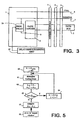
- FIG 3 shows a diagrammatic view of a memory controller 19 embodying the invention together with several memory modules.
- the memory controller 19 of Figure 3 comprises data latches 6 for latching the data coming from the memory modules 3, 4, and 5 on the data bus 2; these memory modules may for instance be comprised of SDRAM modules.
- the data latches 6 are enabled by a strobe signal on an input 9.
- a memory clock signal MEMCLK is present on a clock line 7.
- the strobe signal causes data to be read into the latches 6 every clock cycle, this data being only treated as valid a predetermined number of MEMCLK cycles after assertion of the CTRL signal.
- the memory controller 19 comprises programmable means 20 for producing the strobe signal in a programmed timing relation to the clock signal MEMCLK.
- These programmable means can be used for programming the strobe delay according to the memory configuration, so as to ensure correct data reading relative to the CTRL signal (it being possible to time the strobe signal from the MEMCLK signal because the memory data read signal CTRL is also timed from the MEMCLK signal).
- the means 20 may for instance comprise a programmable delay line connected between the memory clock line 7 and the enabling input 9 of the data latches 6.
- This programmable delay line may comprise a programmable register that determines the delay duration in known manner. This makes the programming of the strobe delay easy to implement, through a simple software programming of one register of the memory controller.
- the range and granularity of the strobe delay may depend on the implementation. As an example, a range of 2 to 10 nanoseconds, and a granularity of 150 picoseconds were found to be sufficient for a memory controller accessing up to 4 memory SDRAM modules, at a clock frequency of 125 MHz. If the programmable means 20 comprise a register of the memory controller the size of this register is determined by the range and granularity of the strobe delay.
- Figure 3 only shows the components of the memory controller necessary for the understanding of the present invention.
- the other components of the memory controller 19 are not represented.
- the memory controller will include circuitry for enabling reading of the data latches 6 only a predetermined number of MEMCLK cycles after assertion of the CTRL and this circuitry is not represented in Figure 3.
- the memory controllers embodying this invention allow programming of the strobe signal delay according to the circumstances, for instance according to memory modules configuration, according to memory load, and so on. It allows the memory controller to run at full speed reliably in any memory configuration, notwithstanding variations in load on the memory bus and the actual configuration of the memory controller.
- the means 20 for deriving the strobe signal are programmed by a delay-programming functional block or unit 25 at power-on of the memory controller, to ensure that any change in the memory configuration is properly taken into account. It is also possible to proceed with the programming whenever a change of the memory configuration is detected.
- the unit 25 for programming the programmable means 20 may take the form of dedicated hardware circuitry provided internally or externally of the memory controller or by a system microprocessor operating under firmware control.
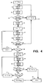
- Figure 4 is a flow chart of a method for programming the strobe signal delay in accordance with the invention.
- the method of Figure 4 is a simple and quick method for programming the means 20 for deriving the strobe signal.
- the means 20 for deriving the strobe signal can be programmed to set a delay ⁇ between the memory clock signal and the strobe signal.
- the delay ⁇ may be programmed in a range ⁇ min - ⁇ max , with a granularity of g.
- the program determines a lowest value ⁇ _ ensuring a correct reading of the data from the memory.
- step 30 the delay ⁇ is set to the minimum value ⁇ min .
- the program proceeds to step 31.
- step 31 data is written into the memory.
- the program proceeds to step 32.
- step 32 data is read from the memory.
- the program proceeds to step 33.
- step 33 the data read from the memory is compared to the data written into the memory. If the data read and written are different, the program proceeds to step 34. If the data read and written are not different, the program proceeds to step 35.
- step 34 the delay is incremented by g.
- the program then proceeds to step 31.
- step 35 ⁇ has a value which has already produced one correct reading of the data in the memory.
- this value is checked in steps 36-41 to ensure that this value of ⁇ gives correct reading of data for more than one operation.
- This reliability test is not compulsory, and may be skipped. In this case, the program proceeds directly to step 42.
- step 36 the reliability of the write/read operation with the current value of ⁇ is checked, by performing i max write and read operations.
- step 36 a parameter i is set at 1. The program proceeds to step 37.
- step 37 data is written into the memory.
- the program proceeds to step 38.
- step 38 data is read from the memory.
- the program proceeds to step 39.
- step 39 the data read from the memory is compared to the data written into the memory. If the data read and written are different, it is determined that the current value of ⁇ is not reliable; the program proceeds to step 34. If the data read and written are the same, the program proceeds to step 40.
- step 41 i is incremented by 1. The program then proceeds to step 37.
- step 42 the current value of ⁇ is stored as ⁇ _; this value of ⁇ is the lowest value for which the reading of the data is successful. The value of ⁇ is then incremented by g. The program then proceeds to step 43.
- steps 43-49 the program determines a value ⁇ + for the delay.
- ⁇ + for the delay.
- data may be read correctly from the memory.
- step 43 data is written into the memory.
- the program proceeds to step 44.
- step 44 data is read from the memory.
- the program proceeds to step 45.
- step 45 the data read from the memory is compared to the data written into the memory. If the data read and written are identical, the program proceeds to step 46. If the data read and written are different, the program proceeds to step 48.
- step 46 it has been determined that the current value of ⁇ is still resulting in at least one correct reading of the data from the memory. It is possible, optionally, to check whether the current value of ⁇ ensures correct reading for more that one write/read operation. This may be done using program steps similar to steps 36-41: however, this reliability test is not compulsory, and may be skipped.
- step 47 the delay ⁇ is incremented by g.
- the program proceeds to step 43.
- step 48 a value of ⁇ giving at least one incorrect reading of the data in the memory has been reached.
- values of ⁇ between ⁇ _ and ⁇ - g i.e. the current value of ⁇ minus one increment ensure correct reading in the memory.
- the value ⁇ - g is stored as ⁇ + . The program then proceeds to step 50.
- step 49 it has been determined that the values of ⁇ between ⁇ - and ⁇ max result in a correct reading of the data in the memory.
- the value ⁇ max is stored as ⁇ + .
- the program then proceeds to step 50.
- step 50 it has been ascertained that values of ⁇ between ⁇ - and ⁇ + result in correct reading of the data.
- the delay ⁇ may then be programmed at any value within this range, e.g. at the value nearest to ( ⁇ + - ⁇ _)/2 .
- the method of Figure 4 allows for a simple and quick setting of the delay ⁇ . Other methods are possible; the method of Figure 4 may also be modified. For instance, in the flow chart of Figure 4, each reading step follows a writing step; the information which is written into the memory may vary for each write/read operation, to ensure correct statistical check of the memory; however, it would also be possible to have only one writing step, and to read always the same data. It is also possible to start by determining ⁇ + , and then determine ⁇ _, the necessary changes being obvious for the person skilled in the art.
- the whole range of delay values is checked to ascertain whether there exist several appropriate reading windows [ ⁇ _; ⁇ + ]; if this is the case, a value of ⁇ in the largest window is preferably chosen.
- Figure 5 shows a flowchart for this method.
- the delay ⁇ is set to the minimum value ⁇ min .
- a parameter j is set to 1.
- the program proceeds to step 61.
- step 61 a reading range or window [ ⁇ - ; ⁇ + ] is determined, e.g. using steps 31-49 of Figure 4.
- the program proceeds to step 62.
- step 62 the current values of ⁇ - and ⁇ + are stored as ⁇ -j and ⁇ +j .
- the program then proceeds to step 63.
- step 63 ⁇ + is compared to ⁇ max . If ⁇ + is equal to ⁇ max , there cannot be any further appropriate window. In this case, the program proceeds to step 65. If this is not the case, the program proceeds to step 64.
- step 64 j is incremented by one, and ⁇ is incremented by g.
- the program then proceeds to step 61.
- step 65 for all possible values of j, the difference ⁇ +j - ⁇ -j is computed. The largest difference is determined. This provides the largest reading window. The program then proceeds to step 66.
- step 66 delay ⁇ is programmed at any value within this largest reading window, e.g. at the value nearest to ( ⁇ +j - ⁇ -j )/2, j being the index of the largest reading window, as determined in step 65.
- the method of Figure 5 ensures that the value for the delay is chosen in the largest possible range appropriate for reading data from the memory.
- the delay-programming unit 25 can be arranged to incrementally adjust the programmed delay value in dependence on variations in supply voltage and/or temperature whereby to compensate for any undesired drifting of the strobe signal during use of the memory controller.
- the unit 25 further comprises means responsive to changes in the measured parameter value over time to determine an appropriate change in the delay set into the programmable delay 20; these means could take the form of a look-up table. Once an appropriate change in delay has been determined, the unit 25 changes the programmed delay by the appropriate amount.
- the simplest way of producing the strobe signal is to delay either the MEMCLK or CTRL signal as described above, it will be appreciated that other ways are possible.
- a separate clock circuit could be used to generate the strobe signal, this clock circuit being synchronised with the MEMCLK signal in a desired phase relation thereto by a suitable phase-locked loop.
Description
- The present invention relates to a memory controller with a programmable strobe delay. It also relates to a method for programming such a memory controller, and to a method for enhancing the reliability of data reading in a memory controller.
- The invention addresses the problem of reading data from memories. Figure 1 of the accompanying drawings shows a diagrammatic view of a
conventional memory controller 1 together with its associateddata bus 2, andseveral memory modules 3, 4 and 5. The memory controller inter alia comprises a series 6 of data latches connected to thedata bus 2. A memory clock signal MEMCLK is present online 7 in thememory controller 1 and in the different memory modules. Thememory controller 1 may transmit on line 8 a control signal CTRL for reading data from the different memory modules, the timing of this signal being related to the clock signal MEMCLK. Data present on the memory bus may be latched in the data latches 6 when aninput 9 of the latches is enabled by a strobe signal. The memory address control lines and memory write control lines are not represented in Figure 1. - Figure 2 is a timing diagram of different signals in the device of Figure 1. In Figure 2, 10 is the memory clock MEMCLK signal on
line 7. When data is to be read from thememory modules 3, 4, 5, aread signal CTRL 11 is transmitted on line 8. A certain number of memory clock cycles later - say three in the case of Figure 2, theinput 9 of the data latches 6 in the memory controller is enabled for latching the data coming from thememory modules 3, 4, 5, which is present on thedata bus 2.Reference 12 identifies the strobe signal for enabling the data latches 6, whereas 13, 14, and 15 identify the respective data sent on thedata bus 2 by thedifferent memory modules 3, 4, 5.Reference 16 identifies the data window, that is the time period during which the data from thememory modules 3, 4, and 5 may validly be read. - In the Figure 1 system, the delay between the
read control signal 11 and the strobe signal enabling the data latches at theirinput 9 is set by hardware, as shown in Figure 1 by theblock 17 between CTRL line 8 and theinput 9. - It has also been proposed read data into the latches 6 every clock cycle, the strobe signal being generated at an appropriate time in each clock cycle to ensure proper reading of the data bus. However, the contents of the data latches is only considered valid a predetermined number of MEMCLK clock signal edges after assertion of the CTRL signal as counted by any appropriate circuitry. In this approach, the strobe signal is a clock signal formed by a delayed version of the clock signal MEMCLK, the delay between these two clocks being set, for example, by a conductive path of a given length on the memory-controller circuitboard, between two pins of the memory controller.
- The above-described arrangements suffer from several drawbacks. First, they do not address the problem of the effects of changes of configuration in the memory modules, and will therefore not operate for highly loaded and/or very high speed memories. Second, the computation of the strobe-signal delay is a difficult task, and involves numerous experimentations for determining a correct statistical value of the delay.
- The present invention addresses the problem of data reading encountered in heavily loaded or high speed memory configurations. This problem arises where the memory bus is highly loaded, e.g. where there are four memory modules or more on the same memory bus; it also arises at high speed, for example 100 MHz or more for the memory clock, for synchronous memory systems. In this case, the difference of transmission time between the memory modules cannot be neglected: the data window 16 (see Figure 1) for reading the data may become fairly small, and even too small for ensuring correct reading of the data in all possible configurations.
- Indeed, the data from each memory module may be read for a duration which is typically around 4 or 5 ns for a clock frequency of 125 MHz, and the
data window 16 may get reduced by the various skews in the system. - Moreover, the invention addresses the problem arising from the fact that the position and duration of the
data window 16 may depend on the actual load on thememory bus 2, which itself depends on the actual configuration of the memory modules. This configuration is not fixed, and may vary at any time according to the user's wish. These problems make it very difficult to design a memory controller that can run at full speed and reliably latch data whatever the memory configuration. - The present invention provides a solution to the problem of providing a memory controller that may run at full speed reliably in any memory configuration, whatever the load on the memory bus and the actual configuration of the memory controller, and even for very high speeds.
- EP-A-379772 describes a system for providing asynchronous communication between at least one central processing unit and at least one associated memory unit with specially programmed timing signals to latch, select and transmit data between them.
- The disclosure WO-A-98/15897 is a prior art document according to Article 54(3)EPC.
- According to one aspect of the invention, there is provided a system having at least one memory module and a memory controller, the memory controller comprising:
- a clock line for a clock signal;
- data receiving means for connecting to the at least one memory module;
- data latching means connected to the data receiving means, for latching data under control of a strobe signal; and
- programmable means for providing said strobe signal in programmed timing relation
to said clock signal characterised by the system comprising:
- first means for repeatedly measuring the value of a parameter indicative of the signal delay characteristics in the system in order to detect variations therein, and
- second means responsive to variations in said signal delay characteristics detected by said first means, to change the programming of said programmable means to compensate said programmed timing relation for said variations.
- In one embodiment, the programmable means comprise a programmable delay operatively connected between the clock line and the data latching means. In another embodiment, the programmable means comprise a programmable delay operatively connected between a memory-control line and the data latching means, the memory control line serving to carry a memory-read signal produced in timed relation to the clock signal.
- Preferably, delay-programming means are provided for automatically programming the programmable means for providing the strobe signal, the programming means being operative to effect this programming, for example, upon power up of the system including the memory controller.
- The programmable means in such a memory controller can be programmed by:
- (a) - programming the programmable means to a given value;
- (b) -using the memory controller to write data into memory means;
- (c) -using the memory controller to read the data written into the memory means;
- (d) -determining whether the data read in step (b) are identical to the data written in step (c);
- (e) -repeating steps (a) to (d) until step (d) gives a positive result for at least one given value.
- (f) -programming the programmable means to one of said at least one given value. Step (e) may comprise incrementing the given value, and in this case, once step (d) has given a positive result, steps (a) to (d) are repeated until step (d) gives a negative result.Alternatively, step (e) may comprise decrementing the given value, and in this case, once step (d) has given a positive result, steps (a) to (d) are repeated until step (d) gives a negative result.In both cases, step (f) preferably comprises choosing a value among a range of values for which step (d) gives a positive result.It is also possible that step (e) is repeated for all possible programmable values. In this case, step (f) may comprise: (g) determining ranges of values for which step (d) gives a positive result;
- (h) determining the largest of these ranges of values; the programmable means being programmed to a value comprised in the largest of said ranges.
-
- According to a further aspect of the present invention, there is provided a method as defined in
independent claim 12. - Further embodiments of the invention are specified in the appended dependent claims.
- A memory controller embodying the invention will now be described, by way of non-limiting example, with reference to the accompanying drawings, in which:
- Figure 1
- is a diagrammatic view of a conventional memory controller together with several memory modules;
- Figure 2
- is a timing diagram of different signals in the device of Figure 1;
- Figure 3
- is a diagrammatic view of a memory controller embodying the invention together with several memory modules;
- Figure 4
- is a flow chart of a method for programming the strobe signal delay in accordance with the invention.
- Figure 5
- shows a flowchart of another method for programming the strobe signal delay in accordance with the invention.
- Figure 3 shows a diagrammatic view of a memory controller 19 embodying the invention together with several memory modules. The memory controller 19 of Figure 3 comprises data latches 6 for latching the data coming from the
memory modules 3, 4, and 5 on thedata bus 2; these memory modules may for instance be comprised of SDRAM modules. The data latches 6 are enabled by a strobe signal on aninput 9. A memory clock signal MEMCLK is present on aclock line 7. In the same general manner described above in relation to the prior art, the strobe signal causes data to be read into the latches 6 every clock cycle, this data being only treated as valid a predetermined number of MEMCLK cycles after assertion of the CTRL signal. - In accordance with the present invention the memory controller 19 comprises programmable means 20 for producing the strobe signal in a programmed timing relation to the clock signal MEMCLK. These programmable means can be used for programming the strobe delay according to the memory configuration, so as to ensure correct data reading relative to the CTRL signal (it being possible to time the strobe signal from the MEMCLK signal because the memory data read signal CTRL is also timed from the MEMCLK signal). As shown in Figure 3, the
means 20 may for instance comprise a programmable delay line connected between thememory clock line 7 and the enablinginput 9 of the data latches 6. This programmable delay line may comprise a programmable register that determines the delay duration in known manner. This makes the programming of the strobe delay easy to implement, through a simple software programming of one register of the memory controller. - The range and granularity of the strobe delay may depend on the implementation. As an example, a range of 2 to 10 nanoseconds, and a granularity of 150 picoseconds were found to be sufficient for a memory controller accessing up to 4 memory SDRAM modules, at a clock frequency of 125 MHz. If the programmable means 20 comprise a register of the memory controller the size of this register is determined by the range and granularity of the strobe delay.
- Figure 3 only shows the components of the memory controller necessary for the understanding of the present invention. The other components of the memory controller 19 are not represented. For instance in the present embodiment the memory controller will include circuitry for enabling reading of the data latches 6 only a predetermined number of MEMCLK cycles after assertion of the CTRL and this circuitry is not represented in Figure 3.
- Of course, it would also be possible to implement the present invention in a memory controller of the Figure 1 form by deriving the strobe signal from the control signal CTRL using a programmable delay line. Because the CTRL signal is timed from the MEMCLK signal, this embodiment like that of Figure 3, times the strobe signal relative to the MEMCLK signal though in this case indirectly.
- Whichever implementation is used, the memory controllers embodying this invention allow programming of the strobe signal delay according to the circumstances, for instance according to memory modules configuration, according to memory load, and so on. It allows the memory controller to run at full speed reliably in any memory configuration, notwithstanding variations in load on the memory bus and the actual configuration of the memory controller.
- As regards the programming of the strobe signal delay into the programmable means, this may be done whenever necessary. In a preferred embodiment of the invention, the
means 20 for deriving the strobe signal are programmed by a delay-programming functional block orunit 25 at power-on of the memory controller, to ensure that any change in the memory configuration is properly taken into account. It is also possible to proceed with the programming whenever a change of the memory configuration is detected. Theunit 25 for programming the programmable means 20 may take the form of dedicated hardware circuitry provided internally or externally of the memory controller or by a system microprocessor operating under firmware control. - Figure 4 is a flow chart of a method for programming the strobe signal delay in accordance with the invention. The method of Figure 4 is a simple and quick method for programming the
means 20 for deriving the strobe signal. In the method of Figure 4, it is assumed that themeans 20 for deriving the strobe signal can be programmed to set a delay Δ between the memory clock signal and the strobe signal. The delay Δ may be programmed in a range Δmin-Δmax, with a granularity of g. - In steps 30-42, the program determines a lowest value Δ_ ensuring a correct reading of the data from the memory.
- In
step 30, the delay Δ is set to the minimum value Δmin. The program proceeds to step 31. - In
step 31, data is written into the memory. The program proceeds to step 32. - In
step 32, data is read from the memory. The program proceeds to step 33. - In
step 33, the data read from the memory is compared to the data written into the memory. If the data read and written are different, the program proceeds to step 34. If the data read and written are not different, the program proceeds to step 35. - In
step 34, the delay is incremented by g. The program then proceeds to step 31. - By
step 35, Δ has a value which has already produced one correct reading of the data in the memory. Preferably, this value is checked in steps 36-41 to ensure that this value of Δ gives correct reading of data for more than one operation. This reliability test is not compulsory, and may be skipped. In this case, the program proceeds directly to step 42. - In steps 36-41, the reliability of the write/read operation with the current value of Δ is checked, by performing imax write and read operations. In
step 36, a parameter i is set at 1. The program proceeds to step 37. - In
step 37, data is written into the memory. The program proceeds to step 38. - In
step 38, data is read from the memory. The program proceeds to step 39. - In
step 39, the data read from the memory is compared to the data written into the memory. If the data read and written are different, it is determined that the current value of Δ is not reliable; the program proceeds to step 34. If the data read and written are the same, the program proceeds to step 40. - In
step 40, it is checked whether imax write and read operations have been performed, that is whether i > = imax. If this is not the case, the program proceeds to step 41. If this is the case, the current value of Δ has proved reliable for imax + 1 write and read operations. The program then proceeds to step 42. - In
step 41, i is incremented by 1. The program then proceeds to step 37. - In
step 42, the current value of Δ is stored as Δ_; this value of Δ is the lowest value for which the reading of the data is successful. The value of Δ is then incremented by g. The program then proceeds to step 43. - In steps 43-49 the program determines a value Δ+ for the delay. In the range from Δ_ to Δ+, data may be read correctly from the memory.
- In
step 43, data is written into the memory. The program proceeds to step 44. - In
step 44, data is read from the memory. The program proceeds to step 45. - In step 45, the data read from the memory is compared to the data written into the memory. If the data read and written are identical, the program proceeds to step 46. If the data read and written are different, the program proceeds to step 48.
- In
step 46, it has been determined that the current value of Δ is still resulting in at least one correct reading of the data from the memory. It is possible, optionally, to check whether the current value of Δ ensures correct reading for more that one write/read operation. This may be done using program steps similar to steps 36-41: however, this reliability test is not compulsory, and may be skipped. The current value of A is then compared to the maximum value Δmax. If Δ = Δmax, the program proceeds to step 49; else, the program proceeds to step 47. - In
step 47, the delay Δ is incremented by g. The program proceeds to step 43. - In
step 48, a value of Δ giving at least one incorrect reading of the data in the memory has been reached. At that step it has been determined that values of Δ between Δ_ and Δ - g, i.e. the current value of Δ minus one increment ensure correct reading in the memory. The value Δ - g is stored as Δ+. The program then proceeds to step 50. - In step 49, it has been determined that the values of Δ between Δ- and Δmax result in a correct reading of the data in the memory. The value Δmax is stored as Δ+. The program then proceeds to step 50.
- By
step 50, it has been ascertained that values of Δ between Δ- and Δ+ result in correct reading of the data. The delay Δ may then be programmed at any value within this range, e.g. at the value nearest to (Δ+ - Δ_)/2 . - The method of Figure 4 allows for a simple and quick setting of the delay Δ. Other methods are possible; the method of Figure 4 may also be modified. For instance, in the flow chart of Figure 4, each reading step follows a writing step; the information which is written into the memory may vary for each write/read operation, to ensure correct statistical check of the memory; however, it would also be possible to have only one writing step, and to read always the same data. It is also possible to start by determining Δ+, and then determine Δ_, the necessary changes being obvious for the person skilled in the art.
- In a preferred embodiment of the invention, the whole range of delay values is checked to ascertain whether there exist several appropriate reading windows [Δ_; Δ+]; if this is the case, a value of Δ in the largest window is preferably chosen. Figure 5 shows a flowchart for this method.
- In the
first step 60, the delay Δ is set to the minimum value Δmin. A parameter j is set to 1. The program proceeds to step 61. - In
step 61, a reading range or window [Δ-; Δ+] is determined, e.g. using steps 31-49 of Figure 4. The program proceeds to step 62. - In
step 62, the current values of Δ- and Δ+ are stored as Δ-j and Δ+j. The program then proceeds to step 63. - In
step 63, Δ+ is compared to Δmax. If Δ+ is equal to Δmax, there cannot be any further appropriate window. In this case, the program proceeds to step 65. If this is not the case, the program proceeds to step 64. - In
step 64, j is incremented by one, and Δ is incremented by g. The program then proceeds to step 61. - In
step 65, for all possible values of j, the difference Δ+j - Δ-j is computed. The largest difference is determined. This provides the largest reading window. The program then proceeds to step 66. - In
step 66, delay Δ is programmed at any value within this largest reading window, e.g. at the value nearest to (Δ+j - Δ-j)/2, j being the index of the largest reading window, as determined instep 65. - The method of Figure 5 ensures that the value for the delay is chosen in the largest possible range appropriate for reading data from the memory.
- The description of the best mode of carrying out the invention was only given as an example. Other embodiments of the invention can be used; for instance, a method other than the one depicted in Figure 4 may be used for programming the strobe signal delay. It is possible to use programming means 20 other than a register in the memory controller, if other suitable programming capabilities are provided.
- In addition to programming in a particular value for the strobe signal delay at predetermined points during system operation, the delay-
programming unit 25 can be arranged to incrementally adjust the programmed delay value in dependence on variations in supply voltage and/or temperature whereby to compensate for any undesired drifting of the strobe signal during use of the memory controller. - This can be implemented by using a circuit for measuring the value of a parameter sensitive to the signal delay characteristics in the memory subsystem. By way of example, the measured parameter could be the number of inverters in a chain of inverters needed to produce a predetermined signal delay. The
unit 25 further comprises means responsive to changes in the measured parameter value over time to determine an appropriate change in the delay set into theprogrammable delay 20; these means could take the form of a look-up table. Once an appropriate change in delay has been determined, theunit 25 changes the programmed delay by the appropriate amount. - Although the simplest way of producing the strobe signal is to delay either the MEMCLK or CTRL signal as described above, it will be appreciated that other ways are possible. For example, a separate clock circuit could be used to generate the strobe signal, this clock circuit being synchronised with the MEMCLK signal in a desired phase relation thereto by a suitable phase-locked loop.
Claims (17)
- A system having at least one memory module (3, 4, 5) and a memory controller (19), the memory controller comprising:a clock line (7) for a clock signal;data receiving means (2) for connecting to the at least one memory module (3, 4, 5);data latching means (6) connected to the data receiving means (2), for latching data under control of a strobe signal; andprogrammable means (20) for providing said strobe signal in programmed timing relation to said clock ignal characterised by the system comprising:first means for periodically measuring the value of a parameter indicative of the signal delay characteristics in the system in order to detect variations therein, andsecond means responsive to variations in said signal delay characteristics detected by said first means, to change the programming of said programmable means to compensate said programmed timing relation for said variations.
- A system according to claim 1, wherein the programmable means (20) comprise a programmable delay operatively connected between said clock line (7) and said data latching means (6).
- A system according to claim 1, further comprising:said programmable means (20) being a programmable delay operatively connected between said memory-control line and said data latching means.a memory control line (8) for a memory-read signal, andmeans for producing said memory-read signal in timed relation to said clock signal;
- A system according to any one of the preceding claims, wherein the programmable means (20) comprise a programmable register for setting said programmed timing relation.
- A system according to claim 4, wherein said programming means effects said programming upon power up of said system.
- A system as claimed in any preceding claim wherein the programmable means comprises means arranged to perform the following steps(a) - programming the programmable means to a given value;(b) -using the memory controller to write data into memory means;(c) -using the memory controller to read the data written into the memory means;(d) -determining whether the data read in step (b) are identical to the data written in step (c);(e) -repeating steps (a) to (d) until step (d) gives a positive result for at least one given value.(f) -programming the programmable means to one of said at least one given value.
- A system as claimed in claim 6, arranged so that said step (e) comprises incrementing said given value, and, once step (d) has given a positive result, steps (a) to (d) are repeated until step (d) gives a negative result.
- A system as claimed in claim 6 arranged so that said step (e) comprises decrementing said given value, and, once step (d) has given a positive result, steps (a) to (d) are repeated until step (d) gives a negative result.
- A system as claimed in claim 7 or claim 8, arranged so that step (f) comprises choosing a value among a range of values for which step (d) gives a positive result.
- A system as claimed in claim 6, arranged so that step (e) is repeated for all possible programmable values.
- A system as claimed in claim 10 arranged so that step (f) comprises:and the programmable means being programmed to a value comprised in the largest of said ranges.(g)determining ranges of values for which step (d) gives a positive result;(h) determining the largest of these ranges of values;
- A method of enhancing the reliability of data reading in a memory controller from at least one memory module within a system, said memory controller comprising data receiving means (2) for connecting to said at least one memory module (3,4,5) and data latching means (6) connected to said data receiving means (2), for latching data under control of said reading strobe signal, said method comprising the step of
programming in programmable means within the memory controller a delay between a clock signal (10) and a reading strobe signal; said method being characterized by the steps of
periodically measuring the value of a parameter indicative of the signal delay characteristics in the system in order to detect variations therein; andresponding to variations in said signal delay characteristics detected by said first means, to change the programming of said delay to compensate said programmed timing relation for said variations. - A method according to claim 12, wherein said programming is carried out at power-on of the memory controller.
- A method according to claim 12, wherein said programming is carried out to compensate for voltage variations.
- A method according to claim 12, wherein said programming is carried out to compensate for variations in processing load.
- A method according to claim 12, wherein said programming is carried out to compensate for temperature variations.
Priority Applications (3)
| Application Number | Priority Date | Filing Date | Title |
|---|---|---|---|
| DE69731066T DE69731066T2 (en) | 1997-01-23 | 1997-01-23 | Memory controller with programmable pulse delay |
| EP97410009A EP0855653B1 (en) | 1997-01-23 | 1997-01-23 | Memory controller with a programmable strobe delay |
| JP10004583A JPH10232818A (en) | 1997-01-23 | 1998-01-13 | Memory controller |
Applications Claiming Priority (1)
| Application Number | Priority Date | Filing Date | Title |
|---|---|---|---|
| EP97410009A EP0855653B1 (en) | 1997-01-23 | 1997-01-23 | Memory controller with a programmable strobe delay |
Publications (2)
| Publication Number | Publication Date |
|---|---|
| EP0855653A1 EP0855653A1 (en) | 1998-07-29 |
| EP0855653B1 true EP0855653B1 (en) | 2004-10-06 |
Family
ID=8229944
Family Applications (1)
| Application Number | Title | Priority Date | Filing Date |
|---|---|---|---|
| EP97410009A Expired - Lifetime EP0855653B1 (en) | 1997-01-23 | 1997-01-23 | Memory controller with a programmable strobe delay |
Country Status (3)
| Country | Link |
|---|---|
| EP (1) | EP0855653B1 (en) |
| JP (1) | JPH10232818A (en) |
| DE (1) | DE69731066T2 (en) |
Cited By (6)
| Publication number | Priority date | Publication date | Assignee | Title |
|---|---|---|---|---|
| EP2014883A2 (en) | 2003-05-10 | 2009-01-14 | Universität Stuttgart | Method and devices for purifying waste gases |
| US8214575B2 (en) | 1997-09-26 | 2012-07-03 | Rambus Inc. | Memory module having signal lines configured for sequential arrival of signals at synchronous memory devices |
| US8214616B2 (en) | 2001-04-24 | 2012-07-03 | Rambus Inc. | Memory controller device having timing offset capability |
| US8283955B2 (en) | 2006-03-13 | 2012-10-09 | Nxp B.V. | Double data rate interface |
| US8320202B2 (en) | 2001-04-24 | 2012-11-27 | Rambus Inc. | Clocked memory system with termination component |
| US9229470B2 (en) | 2004-09-15 | 2016-01-05 | Rambus Inc. | Memory controller with clock-to-strobe skew compensation |
Families Citing this family (12)
| Publication number | Priority date | Publication date | Assignee | Title |
|---|---|---|---|---|
| US7050959B1 (en) | 1999-12-23 | 2006-05-23 | Intel Corporation | Dynamic thermal management for integrated circuits |
| US6578125B2 (en) | 2000-02-14 | 2003-06-10 | Sanyo Electric Co., Ltd. | Memory access circuit and memory access control circuit |
| JP2001337862A (en) * | 2000-05-29 | 2001-12-07 | Fujitsu Ltd | Memory system and method of set up the same |
| WO2002001363A1 (en) * | 2000-06-27 | 2002-01-03 | Matsushita Electric Industrial, Co., Ltd. | Memory control device, and memory control method |
| KR100389916B1 (en) * | 2000-08-28 | 2003-07-04 | 삼성전자주식회사 | Memory module and memory controller |
| US6553472B2 (en) * | 2001-01-12 | 2003-04-22 | Sun Microsystems, Inc. | Method for programming clock delays, command delays, read command parameter delays, and write command parameter delays of a memory controller in a high performance microprocessor |
| EP1253521B1 (en) * | 2001-04-24 | 2011-01-26 | Rambus Inc. | Method and apparatus for signaling between devices of a memory system |
| US6697926B2 (en) * | 2001-06-06 | 2004-02-24 | Micron Technology, Inc. | Method and apparatus for determining actual write latency and accurately aligning the start of data capture with the arrival of data at a memory device |
| US6918048B2 (en) | 2001-06-28 | 2005-07-12 | Intel Corporation | System and method for delaying a strobe signal based on a slave delay base and a master delay adjustment |
| US20040215912A1 (en) * | 2003-04-24 | 2004-10-28 | George Vergis | Method and apparatus to establish, report and adjust system memory usage |
| US7966439B1 (en) * | 2004-11-24 | 2011-06-21 | Nvidia Corporation | Apparatus, system, and method for a fast data return memory controller |
| JPWO2009096141A1 (en) * | 2008-01-29 | 2011-05-26 | パナソニック株式会社 | Memory access timing adjustment device and memory access timing adjustment method |
Citations (1)
| Publication number | Priority date | Publication date | Assignee | Title |
|---|---|---|---|---|
| WO1997015897A1 (en) * | 1995-10-26 | 1997-05-01 | Motorola Inc. | Method and device for encoding/decoding a displaced frame difference |
Family Cites Families (4)
| Publication number | Priority date | Publication date | Assignee | Title |
|---|---|---|---|---|
| US5335337A (en) * | 1989-01-27 | 1994-08-02 | Digital Equipment Corporation | Programmable data transfer timing |
| US5615358A (en) * | 1992-05-28 | 1997-03-25 | Texas Instruments Incorporated | Time skewing arrangement for operating memory in synchronism with a data processor |
| US5509138A (en) * | 1993-03-22 | 1996-04-16 | Compaq Computer Corporation | Method for determining speeds of memory modules |
| US5557782A (en) * | 1994-07-12 | 1996-09-17 | Zenith Data Systems Corporation | Flexible deterministic state machine |
-
1997
- 1997-01-23 EP EP97410009A patent/EP0855653B1/en not_active Expired - Lifetime
- 1997-01-23 DE DE69731066T patent/DE69731066T2/en not_active Expired - Fee Related
-
1998
- 1998-01-13 JP JP10004583A patent/JPH10232818A/en active Pending
Patent Citations (1)
| Publication number | Priority date | Publication date | Assignee | Title |
|---|---|---|---|---|
| WO1997015897A1 (en) * | 1995-10-26 | 1997-05-01 | Motorola Inc. | Method and device for encoding/decoding a displaced frame difference |
Cited By (19)
| Publication number | Priority date | Publication date | Assignee | Title |
|---|---|---|---|---|
| US8364878B2 (en) | 1997-09-26 | 2013-01-29 | Rambus Inc. | Memory module having signal lines configured for sequential arrival of signals at a plurality of memory devices |
| US8214575B2 (en) | 1997-09-26 | 2012-07-03 | Rambus Inc. | Memory module having signal lines configured for sequential arrival of signals at synchronous memory devices |
| US8395951B2 (en) | 2001-04-24 | 2013-03-12 | Rambus Inc. | Memory controller |
| US8625371B2 (en) | 2001-04-24 | 2014-01-07 | Rambus Inc. | Memory component with terminated and unterminated signaling inputs |
| US8320202B2 (en) | 2001-04-24 | 2012-11-27 | Rambus Inc. | Clocked memory system with termination component |
| US8359445B2 (en) | 2001-04-24 | 2013-01-22 | Rambus Inc. | Method and apparatus for signaling between devices of a memory system |
| US8214616B2 (en) | 2001-04-24 | 2012-07-03 | Rambus Inc. | Memory controller device having timing offset capability |
| US8391039B2 (en) | 2001-04-24 | 2013-03-05 | Rambus Inc. | Memory module with termination component |
| US9472262B2 (en) | 2001-04-24 | 2016-10-18 | Rambus Inc. | Memory controller |
| US8462566B2 (en) | 2001-04-24 | 2013-06-11 | Rambus Inc. | Memory module with termination component |
| US8537601B2 (en) | 2001-04-24 | 2013-09-17 | Rambus Inc. | Memory controller with selective data transmission delay |
| US9311976B2 (en) | 2001-04-24 | 2016-04-12 | Rambus Inc. | Memory module |
| US8717837B2 (en) | 2001-04-24 | 2014-05-06 | Rambus Inc. | Memory module |
| US8760944B2 (en) | 2001-04-24 | 2014-06-24 | Rambus Inc. | Memory component that samples command/address signals in response to both edges of a clock signal |
| US9053778B2 (en) | 2001-04-24 | 2015-06-09 | Rambus Inc. | Memory controller that enforces strobe-to-strobe timing offset |
| EP2014883A2 (en) | 2003-05-10 | 2009-01-14 | Universität Stuttgart | Method and devices for purifying waste gases |
| US9229470B2 (en) | 2004-09-15 | 2016-01-05 | Rambus Inc. | Memory controller with clock-to-strobe skew compensation |
| US9437279B2 (en) | 2004-09-15 | 2016-09-06 | Rambus Inc. | Memory controller with clock-to-strobe skew compensation |
| US8283955B2 (en) | 2006-03-13 | 2012-10-09 | Nxp B.V. | Double data rate interface |
Also Published As
| Publication number | Publication date |
|---|---|
| DE69731066T2 (en) | 2005-10-06 |
| JPH10232818A (en) | 1998-09-02 |
| EP0855653A1 (en) | 1998-07-29 |
| DE69731066D1 (en) | 2004-11-11 |
Similar Documents
| Publication | Publication Date | Title |
|---|---|---|
| EP0855653B1 (en) | Memory controller with a programmable strobe delay | |
| US5495593A (en) | Microcontroller device having remotely programmable EPROM and method for programming | |
| US6851016B2 (en) | System latency levelization for read data | |
| US6316980B1 (en) | Calibrating data strobe signal using adjustable delays with feedback | |
| US6456544B1 (en) | Selective forwarding of a strobe based on a predetermined delay following a memory read command | |
| US7145374B2 (en) | Methods and apparatus for delay circuit | |
| EP0897154A2 (en) | Memory controller supporting dram circuits with different operating speeds | |
| CN102347081A (en) | Method for calibrating phase of DQS (bidirectional data strobe) delay for DDR (double data rate) controller and apparatus thereof | |
| JP5577776B2 (en) | Memory control apparatus and mask timing control method | |
| US5870404A (en) | Self-timed circuit having critical path timing detection | |
| JP2006040518A (en) | Nonvolatile memory device for performing ddr operation when outputting data, and data output method | |
| CN101232363B (en) | Phase adjusting function evaluating method, transmission margin measuring method, information processing apparatus | |
| US7796465B2 (en) | Write leveling of memory units designed to receive access requests in a sequential chained topology | |
| US5305277A (en) | Data processing apparatus having address decoder supporting wide range of operational frequencies | |
| KR100532973B1 (en) | A device for controlling the data output driver of a memory device | |
| US6968436B2 (en) | Memory controller that controls supply timing of read data | |
| JPH027530B2 (en) | ||
| KR20080005294A (en) | Measure-initialized delay locked loop with live measurement | |
| US5235699A (en) | Timing calibrate and track control circuit | |
| KR102547449B1 (en) | Tester for integrated circuits on a silicon wafer and integrated circuit | |
| JP3039631B2 (en) | Signal line monitoring device | |
| JPH0143392B2 (en) | ||
| JP2588528B2 (en) | Memory mounting detection circuit | |
| JPH11316619A (en) | Clock skew control circuit | |
| KR100415086B1 (en) | Embedded flash micro control unit and method for control the same |
Legal Events
| Date | Code | Title | Description |
|---|---|---|---|
| PUAI | Public reference made under article 153(3) epc to a published international application that has entered the european phase |
Free format text: ORIGINAL CODE: 0009012 |
|
| AK | Designated contracting states |
Kind code of ref document: A1 Designated state(s): DE FR GB |
|
| AX | Request for extension of the european patent |
Free format text: AL;LT;LV;RO;SI |
|
| 17P | Request for examination filed |
Effective date: 19990102 |
|
| AKX | Designation fees paid |
Free format text: DE FR GB |
|
| RBV | Designated contracting states (corrected) |
Designated state(s): DE FR GB |
|
| RAP1 | Party data changed (applicant data changed or rights of an application transferred) |
Owner name: HEWLETT-PACKARD COMPANY, A DELAWARE CORPORATION |
|
| 17Q | First examination report despatched |
Effective date: 20031215 |
|
| GRAP | Despatch of communication of intention to grant a patent |
Free format text: ORIGINAL CODE: EPIDOSNIGR1 |
|
| GRAS | Grant fee paid |
Free format text: ORIGINAL CODE: EPIDOSNIGR3 |
|
| GRAA | (expected) grant |
Free format text: ORIGINAL CODE: 0009210 |
|
| AK | Designated contracting states |
Kind code of ref document: B1 Designated state(s): DE FR GB |
|
| REG | Reference to a national code |
Ref country code: GB Ref legal event code: FG4D |
|
| REF | Corresponds to: |
Ref document number: 69731066 Country of ref document: DE Date of ref document: 20041111 Kind code of ref document: P |
|
| ET | Fr: translation filed | ||
| PLBE | No opposition filed within time limit |
Free format text: ORIGINAL CODE: 0009261 |
|
| STAA | Information on the status of an ep patent application or granted ep patent |
Free format text: STATUS: NO OPPOSITION FILED WITHIN TIME LIMIT |
|
| 26N | No opposition filed |
Effective date: 20050707 |
|
| PGFP | Annual fee paid to national office [announced via postgrant information from national office to epo] |
Ref country code: GB Payment date: 20070125 Year of fee payment: 11 |
|
| PGFP | Annual fee paid to national office [announced via postgrant information from national office to epo] |
Ref country code: DE Payment date: 20070228 Year of fee payment: 11 |
|
| PGFP | Annual fee paid to national office [announced via postgrant information from national office to epo] |
Ref country code: FR Payment date: 20070207 Year of fee payment: 11 |
|
| GBPC | Gb: european patent ceased through non-payment of renewal fee |
Effective date: 20080123 |
|
| PG25 | Lapsed in a contracting state [announced via postgrant information from national office to epo] |
Ref country code: DE Free format text: LAPSE BECAUSE OF NON-PAYMENT OF DUE FEES Effective date: 20080801 |
|
| REG | Reference to a national code |
Ref country code: FR Ref legal event code: ST Effective date: 20081029 |
|
| PG25 | Lapsed in a contracting state [announced via postgrant information from national office to epo] |
Ref country code: GB Free format text: LAPSE BECAUSE OF NON-PAYMENT OF DUE FEES Effective date: 20080123 |
|
| PG25 | Lapsed in a contracting state [announced via postgrant information from national office to epo] |
Ref country code: FR Free format text: LAPSE BECAUSE OF NON-PAYMENT OF DUE FEES Effective date: 20080131 |