EP0859255A2 - Optical coupling structure using gel resin - Google Patents
Optical coupling structure using gel resin Download PDFInfo
- Publication number
- EP0859255A2 EP0859255A2 EP98102548A EP98102548A EP0859255A2 EP 0859255 A2 EP0859255 A2 EP 0859255A2 EP 98102548 A EP98102548 A EP 98102548A EP 98102548 A EP98102548 A EP 98102548A EP 0859255 A2 EP0859255 A2 EP 0859255A2
- Authority
- EP
- European Patent Office
- Prior art keywords
- resin
- coupling system
- optical fiber
- optical
- optical coupling
- Prior art date
- Legal status (The legal status is an assumption and is not a legal conclusion. Google has not performed a legal analysis and makes no representation as to the accuracy of the status listed.)
- Withdrawn
Links
Images


Classifications
-
- G—PHYSICS
- G02—OPTICS
- G02B—OPTICAL ELEMENTS, SYSTEMS OR APPARATUS
- G02B6/00—Light guides; Structural details of arrangements comprising light guides and other optical elements, e.g. couplings
- G02B6/24—Coupling light guides
- G02B6/42—Coupling light guides with opto-electronic elements
- G02B6/4201—Packages, e.g. shape, construction, internal or external details
- G02B6/4204—Packages, e.g. shape, construction, internal or external details the coupling comprising intermediate optical elements, e.g. lenses, holograms
- G02B6/4212—Packages, e.g. shape, construction, internal or external details the coupling comprising intermediate optical elements, e.g. lenses, holograms the intermediate optical element being a coupling medium interposed therebetween, e.g. epoxy resin, refractive index matching material, index grease, matching liquid or gel
Definitions
- This invention relates to an optical coupling system of optical modules used in optical communication apparatus and an airtight-seal mounting structure for such an optical coupling system.
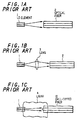
- FIGS.1A and 1B conventional optical coupling systems between LD(semiconductor laser) and an optical fiber to be used in an optical module are shown in FIGS.1A and 1B.
- the first system is so composed that a LD element 1 and an optical fiber 2 are, as shown in FIG.1A, directly optically coupled.
- the second system is so composed that a lens 3 is, as shown in FIG.1B, inserted between the LD element 1 and the optical fiber 2, whereby light beams to be emitted from the LD element 1 are converged and coupled to the optical fiber 2.
- liquid 4 with a proper refractive index as a refractive-index controlling material is, as shown in FIG.1C, injected to relax the coupling tolerance.
- the process of injecting liquid 4 into the optical module and the airtight sealing process are complicated. Therefore, the productivity must be lowered.
- the conventional airtight sealing structure of the optical module is given by mounting an optical coupling system in a package(PKG) made of metal or ceramic, thereafter airtightly sealing a metal or ceramic cap by using seam welding, glass seal, solder seal etc.
- the conventional coupling systems between the LD element and the optical fiber have several problems.
- the direct coupling system shown in FIG.1A which can be cheap fabricated as having the simple structure, has a low coupling efficiency between the LD element 1 and the optical fiber 2 since the spot sizes of the LD element 1 and the optical fiber 2 are different from each other, so that the optical power of the optical module cannot be increased.
- the optical coupling system using the lens 3 as shown in FIG.1B in which the coupling efficiency can be enhanced since the beams emitted from the LD element 1 is converged, needs to fix the three components, i.e., LD element 1, lens 3 and optical fiber 2 when fabricating the optical module, thereby complicating the fabrication. Further, the optical axis needs to be regulated precisely. Thus, the productivity of the optical module must be lowered.
- an optical coupling system comprises a LD element and an optical fiber to be optically coupled with the LD element, wherein the optical coupling system is filled with optically transparent gel resin with a refractive index higher than that of the air and lower than that of the optical fiber.
- a mounting structure comprises: an optical coupling system comprising a LD element and an optical fiber to be optically coupled with the LD element; and a substrate including an electric circuit; wherein the optical coupling system is mounted on the substrate, the optical coupling system is filled with optically transparent gel resin with a refractive index higher than that of the air and lower than that of the optical fiber, the optical coupling system is surrounded by the gel resin and the surface of the gel resin is covered with moisture-blocking resin, and the optical coupling system and a predetermined IC of the electric circuit are covered with the moisture blocking resin.
- a mounting structure comprises: an optical coupling system comprising a LD element and an optical fiber to be optically coupled with the LD element; and a substrate on which the LD element and the optical fiber are mounted; wherein the optical coupling system is filled with first resin which is optically transparent and is solidified into gel state.
- a mounting structure comprises: an optical coupling system comprising a LD element and an optical fiber to be optically coupled with the LD element; a substrate on which the LD element and the optical fiber are mounted; and an interface substrate which includes an electric circuit for driving and controlling the LD element, the substrate being mounted on the interface substrate; wherein the optical coupling system is filled with first resin which is optically transparent and is solidified into gel state, and the surface of the first resin and a predetermined electronic part, wiring or integrated circuit on the interface substrate are covered with second resin to block moisture.
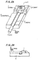
- FIG.2A is a perspective view showing the optical coupling system
- FIG.2B is a partial cross sectional view cut along the line X-X' in FIG.2A.
- the optical coupling system in the embodiment is fabricated by mounting aid optical fiber 2, which is disposed on a V-groove 5 of a silicon substrate 6, and a LD element 1 on the silicon substrate 6 without any regulation, thereafter filling the clearance between the LD element 1 and the optical fiber 2 with liquid silicon resin 7.
- the apparent spot size of light beams emitted from the LD element 1 can be enlarged, thereby enhancing the coupling efficiency to the optical fiber 2.
- the coupling tolerance can be relaxed, thereby providing easily an optical coupling system with a high efficiency.
- FIG.3A is a perspective view showing the mounting structure and FIG.3B is a partial cross sectional view cut along the line X-X' in FIG.3A.
- the surface of resin 7 with which the optical coupling system is covered is further covered with resin 8 for blocking the permeation of moisture.
- resin 8 for blocking the permeation of moisture.
- FIGS.2A and 2B show the high-efficiency optical coupling system using the gel silicon resin 7.
- a marker for the mounting of the LD element 1 is formed on the silicon substrate by patterning, and the V-groove 5 for the guiding of the fiber is formed by silicon anisotropic etching.
- the normal optical fiber 2 or the ball-tipped fiber 10 which has, as shown in FIG.2B, a hemispherical tip portion formed by etching etc. and the LD element 1 are mounted without any regulation. Then, the clearance between the LD element 1 and the optical fiber 2 or 10 is filled with liquid silicon resin 7.
- the tolerance in the optimum coupling of the LD element 1 and optical fiber 2 becomes less than 1 ⁇ m. Namely, the high-precision mounting of both the LD element 1 and optical fiber 2 is required.
- the refractive index of gel silicon resin 7 lies between that of the air and that of the optical fiber. Therefore, the spot size of beams emitted from the LD element 1 can be enlarged, thereby increasing the coupling tolerance to the optical fiber.
- the optical coupling system in this embodiment which has the simple composition employing resin, can realize the high-efficiency coupling of the LD element and the optical fiber 2 without any regulation.
- FIGS.3A and 3B show an example where gel silicon rein 7 and moisture-blocking resin 8 are used for the airtight sealing of the optical system.
- the coupling of the LD element 1 and the optical fiber 2 is, as described earlier, easily conducted on the silicon substrate 6 without any regulation by using gel silicon resin 7. Then, the surface of gel silicon resin 7 with which the optical coupling system is covered is further covered with resin 8 for blocking the permeation of moisture.
- the coupling tolerance(2 dB down) is relaxed to be greater than 20 ⁇ m in the optical axis direction as shown in FIG.5A and to be greater than 1.5 ⁇ m in the perpendicular direction of optical axis as shown in FIG.5B. Therefore, the high-efficiency optical coupling system using the silicon substrate 6 can be realized without any regulation.
- FIG.5A shows a relation between the distance ( ⁇ m) between the LD element and optical fiber and the coupling loss (dB)
- FIG.5B shows a relation between the amount of shifting ( ⁇ m) in the direction perpendicular to the optical axis and the coupling loss (dB).
- the filling process into the optical system can be facilitated and the workability can be improved as compared the filling process of liquid in the conventional optical coupling system. Furthermore, since gel resin has a high elasticity, it can be filled without applying any stress to the optical fiber or IC wiring.
- FIG.4A is a perspective view showing the mounting structure and FIG.4B is a partial cross sectional view cut along the line X-X' in FIG.3A.
- the optical coupling system using gel silicon resin 7 as explained in the above embodiments is directly mounted on an interface substrate 11 where LSI 9 for driving the LD element etc. is mounted. Then, the optical coupling system and LSI 9 are covered with the moisture-blocking resin 8.
- the conventional processes that the optical coupling system is mounted in a package, airtight-sealed and then mounted on the interface substrate 11 are not necessary.
- the interface substrate 11 can be easily fabricated.
- the shield effect for LSI 9 can be also obtained thereby.
Abstract
Description
wherein the optical coupling system is mounted on the substrate, the optical coupling system is filled with optically transparent gel resin with a refractive index higher than that of the air and lower than that of the optical fiber, the optical coupling system is surrounded by the gel resin and the surface of the gel resin is covered with moisture-blocking resin, and the optical coupling system and a predetermined IC of the electric circuit are covered with the moisture blocking resin.
wherein the optical coupling system is filled with first resin which is optically transparent and is solidified into gel state.
wherein the optical coupling system is filled with first resin which is optically transparent and is solidified into gel state, and the surface of the first resin and a predetermined electronic part, wiring or integrated circuit on the interface substrate are covered with second resin to block moisture.
Claims (11)
- An optical coupling system, comprising a LD element and an optical fiber to be optically coupled with said LD element, wherein said optical coupling system is filled with optically transparent gel resin with a refractive index higher than that of the air and lower than that of said optical fiber.
- An optical coupling system, according to claim 1, wherein;
said optical coupling system is surrounded by said gel resin and the surface of said gel resin is covered with moisture-blocking resin. - A mounting structure, comprising an optical coupling system comprising a LD element and an optical fiber to be optically coupled with said LD element, and a substrate including an electric circuit,
wherein said optical coupling system is mounted on said substrate, said optical coupling system is filled with optically transparent gel resin with a refractive index higher than that of the air and lower than that of said optical fiber, said optical coupling system is surrounded by said gel resin and the surface of said gel resin is covered with moisture-blocking resin, and said optical coupling system and a predetermined IC of said electric circuit are covered with said moisture-blocking resin. - A mounting structure, according to claim 3, wherein:conductive resin is used as said moisture-blocking resin in order to give electrical shield to said IC and said optical coupling system.
- A mounting structure, comprising an optical coupling system comprising a LD element and an optical fiber to be optically coupled with said LD element, and a substrate on which said LD element and said optical fiber are mounted,
wherein said optical coupling system is filled with first resin which is optically transparent and is solidified into gel state. - A mounting structure, according to claim 5, wherein:said first resin has a refractive index that is higher than that of the air and lower than that of said optical fiber.
- A mounting structure, according to claim 5 or 6, wherein:the surface of said first resin is covered with second resin to block moisture.
- A mounting structure, comprising an optical coupling system comprising a LD element and an optical fiber to be optically coupled with said LD element, a substrate on which said LD element and said optical fiber are mounted, and an interface substrate which includes an electric circuit for driving and controlling said LD element, said substrate being mounted on said interface substrate,
wherein said optical coupling system is filled with first resin which is optically transparent and is solidified into gel state, and the surface of said first resin and a predetermined electronic part, wiring or integrated circuit on said interface substrate are covered with second resin to block moisture. - A mounting structure, according to claim 8, wherein;said first resin has a refractive index that is higher than that of the air and lower than that of said optical fiber.
- A mounting structure, according to claim 8 or 9, wherein:said optical fiber is a ball-tipped optical fiber.
- A mounting structure, according to any one of claims 5 to 10, wherein:said substrate is of a silicon substrate and said first resin is of silicon resin.
Applications Claiming Priority (2)
| Application Number | Priority Date | Filing Date | Title |
|---|---|---|---|
| JP09044717A JP3087676B2 (en) | 1997-02-13 | 1997-02-13 | Optical coupling system and mounting structure using gel resin |
| JP44717/97 | 1997-02-13 |
Publications (2)
| Publication Number | Publication Date |
|---|---|
| EP0859255A2 true EP0859255A2 (en) | 1998-08-19 |
| EP0859255A3 EP0859255A3 (en) | 1999-03-03 |
Family
ID=12699183
Family Applications (1)
| Application Number | Title | Priority Date | Filing Date |
|---|---|---|---|
| EP98102548A Withdrawn EP0859255A3 (en) | 1997-02-13 | 1998-02-13 | Optical coupling structure using gel resin |
Country Status (4)
| Country | Link |
|---|---|
| US (1) | US6075911A (en) |
| EP (1) | EP0859255A3 (en) |
| JP (1) | JP3087676B2 (en) |
| CA (1) | CA2229570A1 (en) |
Cited By (6)
| Publication number | Priority date | Publication date | Assignee | Title |
|---|---|---|---|---|
| FR2783094A1 (en) * | 1998-09-08 | 2000-03-10 | Fujitsu Ltd | Optical semiconductor module, useful for multimedia optical networks, comprises a resin gel covering an optical semiconductor element and filling the light transmission space between the element and an optical element |
| WO2001057563A2 (en) * | 2000-02-02 | 2001-08-09 | Scc Special Communication Cables Gmbh & Co Kg | Immersion agent, coupling device and method for coupling an optical waveguide |
| WO2002057827A1 (en) * | 2001-01-19 | 2002-07-25 | Alcatel | Passive compensating coupling laser device |
| EP1251607A2 (en) * | 2001-04-20 | 2002-10-23 | Sharp Kabushiki Kaisha | Semiconductor laser module, spatial optical transmission system and electronic appliance |
| EP1258761A2 (en) * | 2001-05-15 | 2002-11-20 | Oki Electric Industry Co., Ltd. | Optical assembly associating a lens with an active element |
| EP1391763A1 (en) * | 2002-08-13 | 2004-02-25 | Tyco Electronics AMP GmbH | Optoelectronic module |
Families Citing this family (35)
| Publication number | Priority date | Publication date | Assignee | Title |
|---|---|---|---|---|
| US6280102B1 (en) * | 1998-02-20 | 2001-08-28 | Sumitomo Electric Industries, Ltd. | Optical module product with sealing cap |
| JP2000098188A (en) * | 1998-09-18 | 2000-04-07 | Fujitsu Ltd | Optical module |
| JP2000110176A (en) * | 1998-10-02 | 2000-04-18 | Fujitsu Ltd | Optical module and manufacture thereof |
| US6315465B1 (en) * | 1998-12-21 | 2001-11-13 | Sumitomo Electric Industries, Ltd. | Optical module |
| JP2001074987A (en) * | 1999-09-08 | 2001-03-23 | Yazaki Corp | Manufacturing method of receptacle, receptacle, and optical connector |
| JP3721923B2 (en) * | 2000-02-22 | 2005-11-30 | 株式会社日立製作所 | Optical module |
| JP2001264593A (en) * | 2000-03-22 | 2001-09-26 | Sumitomo Electric Ind Ltd | Optical device |
| US6345139B1 (en) * | 2000-04-04 | 2002-02-05 | Kabushiki Kaisha Toshiba | Semiconductor light emitting element coupled with optical fiber |
| JP3721935B2 (en) * | 2000-04-19 | 2005-11-30 | 住友電気工業株式会社 | Optical device |
| JP3872984B2 (en) * | 2000-04-27 | 2007-01-24 | 株式会社巴川製紙所 | Optical connection parts |
| JP4134499B2 (en) * | 2000-08-07 | 2008-08-20 | 住友電気工業株式会社 | Optical device |
| US6905260B2 (en) * | 2000-12-26 | 2005-06-14 | Emcore Corporation | Method and apparatus for coupling optical elements to optoelectronic devices for manufacturing optical transceiver modules |
| US6863444B2 (en) * | 2000-12-26 | 2005-03-08 | Emcore Corporation | Housing and mounting structure |
| US6867377B2 (en) * | 2000-12-26 | 2005-03-15 | Emcore Corporation | Apparatus and method of using flexible printed circuit board in optical transceiver device |
| US6799902B2 (en) | 2000-12-26 | 2004-10-05 | Emcore Corporation | Optoelectronic mounting structure |
| US6921920B2 (en) * | 2001-08-31 | 2005-07-26 | Smith & Nephew, Inc. | Solid-state light source |
| US7123798B2 (en) * | 2002-03-29 | 2006-10-17 | Ngk Insulators, Ltd. | Optical device and method of producing the same |
| JP3792174B2 (en) * | 2002-05-02 | 2006-07-05 | 株式会社巴川製紙所 | Optical connection parts |
| JP2004200399A (en) * | 2002-12-18 | 2004-07-15 | Tdk Corp | Optical module and its manufacturing method |
| US7321703B2 (en) | 2002-12-20 | 2008-01-22 | Ngk Insulators, Ltd. | Optical device |
| US7195402B2 (en) * | 2002-12-20 | 2007-03-27 | Ngk Insulators, Ltd. | Optical device |
| JPWO2004057396A1 (en) * | 2002-12-20 | 2006-04-27 | 日本碍子株式会社 | Optical device |
| US7308174B2 (en) | 2002-12-20 | 2007-12-11 | Ngk Insulators, Ltd. | Optical device including a filter member for dividing a portion of signal light |
| US6863453B2 (en) * | 2003-01-28 | 2005-03-08 | Emcore Corporation | Method and apparatus for parallel optical transceiver module assembly |
| WO2004109354A1 (en) | 2003-06-02 | 2004-12-16 | Ngk Insulators, Ltd. | Optical device |
| US7452140B2 (en) * | 2003-07-16 | 2008-11-18 | Ibiden Co., Ltd. | Protective sealing of optoelectronic modules |
| ATE549651T1 (en) | 2003-07-24 | 2012-03-15 | Reflex Photonique Inc Reflex Photonics Inc | SCREEN PRINTING METHOD FOR ENCAPSULATING OPTOELECTRONIC CHIPS |
| JP4180537B2 (en) * | 2003-10-31 | 2008-11-12 | シャープ株式会社 | Optical element sealing structure, optical coupler, and optical element sealing method |
| US7553680B2 (en) * | 2004-08-09 | 2009-06-30 | Delphi Technologies, Inc. | Methods to provide and expose a diagnostic connector on overmolded electronic packages |
| US8323789B2 (en) | 2006-08-31 | 2012-12-04 | Cambridge Enterprise Limited | Nanomaterial polymer compositions and uses thereof |
| US20100002324A1 (en) * | 2006-08-31 | 2010-01-07 | Cambridge Enterprise Limited | Optical Nanomaterial Compositions |
| JP4892457B2 (en) * | 2007-11-06 | 2012-03-07 | 日東電工株式会社 | Manufacturing method of optical waveguide device and optical waveguide device obtained thereby |
| JP2014077914A (en) * | 2012-10-11 | 2014-05-01 | Rohm Co Ltd | Optical communication module and manufacturing method therefor |
| JP2014077915A (en) * | 2012-10-11 | 2014-05-01 | Rohm Co Ltd | Optical communication module and manufacturing method therefor |
| JP6491418B2 (en) * | 2014-03-14 | 2019-03-27 | 日立金属株式会社 | Fiber optic connector |
Citations (5)
| Publication number | Priority date | Publication date | Assignee | Title |
|---|---|---|---|---|
| US4359773A (en) * | 1980-07-07 | 1982-11-16 | Bell Telephone Laboratories, Incorporated | Semiconductor lasers with selective driving circuit |
| JPS6190108A (en) * | 1984-10-09 | 1986-05-08 | Nec Corp | Coupling structure between laser diode and optical fiber |
| US5226052A (en) * | 1990-05-08 | 1993-07-06 | Rohm, Ltd. | Laser diode system for cutting off the environment from the laser diode |
| EP0559365A2 (en) * | 1992-03-02 | 1993-09-08 | Motorola, Inc. | Electrical to optical links using metalization |
| EP0589711A2 (en) * | 1992-09-25 | 1994-03-30 | Nec Corporation | Optical coupling equipment for an optical semiconductor and an optical fiber |
Family Cites Families (15)
| Publication number | Priority date | Publication date | Assignee | Title |
|---|---|---|---|---|
| JPS582B2 (en) * | 1978-03-31 | 1983-01-05 | ケイディディ株式会社 | Feedthrough for optical submarine repeaters |
| US4186996A (en) * | 1978-09-22 | 1980-02-05 | Amp Incorporated | Optic adaptor junction |
| JPS6289914A (en) * | 1985-05-31 | 1987-04-24 | Sumitomo Electric Ind Ltd | Optical waveguide integrated with optical element and its production |
| JPS6314489A (en) * | 1986-07-04 | 1988-01-21 | Mitsubishi Electric Corp | Semiconductor laser device |
| JPS6390108A (en) * | 1986-10-03 | 1988-04-21 | Toshiba Corp | Cryostat |
| JPS63100790A (en) * | 1986-10-17 | 1988-05-02 | Nec Corp | Semiconductor laser module |
| US5121457A (en) * | 1991-05-21 | 1992-06-09 | Gte Laboratories Incorporated | Method for coupling laser array to optical fiber array |
| DE4232608C2 (en) * | 1992-09-29 | 1994-10-06 | Bosch Gmbh Robert | Method for manufacturing a cover for an integrated optical circuit |
| US5416871A (en) * | 1993-04-09 | 1995-05-16 | Sumitomo Electric Industries, Ltd. | Molded optical connector module |
| CN1136456C (en) * | 1993-07-07 | 2004-01-28 | Nec东金株式会社 | Optical electric field sensor |
| US5546489A (en) * | 1993-08-02 | 1996-08-13 | Sumitomo Electric Industries, Ltd. | Optical link apparatus |
| JP2630236B2 (en) * | 1993-12-20 | 1997-07-16 | 日本電気株式会社 | Optical transceiver |
| JPH10505433A (en) * | 1994-06-29 | 1998-05-26 | ブリテイッシュ・テレコミュニケーションズ・パブリック・リミテッド・カンパニー | Packaged optical device |
| JP3334829B2 (en) * | 1995-03-08 | 2002-10-15 | 日本電信電話株式会社 | Optical semiconductor module |
| JP2817778B2 (en) * | 1995-08-21 | 1998-10-30 | 日本電気株式会社 | Optical module and manufacturing method thereof |
-
1997
- 1997-02-13 JP JP09044717A patent/JP3087676B2/en not_active Expired - Fee Related
-
1998
- 1998-02-12 CA CA002229570A patent/CA2229570A1/en not_active Abandoned
- 1998-02-13 US US09/023,213 patent/US6075911A/en not_active Expired - Lifetime
- 1998-02-13 EP EP98102548A patent/EP0859255A3/en not_active Withdrawn
Patent Citations (5)
| Publication number | Priority date | Publication date | Assignee | Title |
|---|---|---|---|---|
| US4359773A (en) * | 1980-07-07 | 1982-11-16 | Bell Telephone Laboratories, Incorporated | Semiconductor lasers with selective driving circuit |
| JPS6190108A (en) * | 1984-10-09 | 1986-05-08 | Nec Corp | Coupling structure between laser diode and optical fiber |
| US5226052A (en) * | 1990-05-08 | 1993-07-06 | Rohm, Ltd. | Laser diode system for cutting off the environment from the laser diode |
| EP0559365A2 (en) * | 1992-03-02 | 1993-09-08 | Motorola, Inc. | Electrical to optical links using metalization |
| EP0589711A2 (en) * | 1992-09-25 | 1994-03-30 | Nec Corporation | Optical coupling equipment for an optical semiconductor and an optical fiber |
Non-Patent Citations (1)
| Title |
|---|
| PATENT ABSTRACTS OF JAPAN vol. 010, no. 264 (P-495), 9 September 1986 & JP 61 090108 A (NEC CORP), 8 May 1986 * |
Cited By (15)
| Publication number | Priority date | Publication date | Assignee | Title |
|---|---|---|---|---|
| FR2783094A1 (en) * | 1998-09-08 | 2000-03-10 | Fujitsu Ltd | Optical semiconductor module, useful for multimedia optical networks, comprises a resin gel covering an optical semiconductor element and filling the light transmission space between the element and an optical element |
| DE19942470B4 (en) * | 1998-09-08 | 2013-04-11 | Fujitsu Ltd. | Optical semiconductor module and method for manufacturing an optical semiconductor module |
| WO2001057563A2 (en) * | 2000-02-02 | 2001-08-09 | Scc Special Communication Cables Gmbh & Co Kg | Immersion agent, coupling device and method for coupling an optical waveguide |
| WO2001057563A3 (en) * | 2000-02-02 | 2002-02-28 | Scc Special Comm Cables Gmbh | Immersion agent, coupling device and method for coupling an optical waveguide |
| US6853777B2 (en) | 2000-02-02 | 2005-02-08 | Corning Incorporated | Immersion agent, coupling device and method for coupling an optical waveguide |
| US7054527B2 (en) | 2001-01-19 | 2006-05-30 | Avanex Corporation | Passive compensating coupling laser device |
| WO2002057827A1 (en) * | 2001-01-19 | 2002-07-25 | Alcatel | Passive compensating coupling laser device |
| FR2819895A1 (en) * | 2001-01-19 | 2002-07-26 | Cit Alcatel | LASER DEVICE WITH PASSIVE COMPENSATOR COUPLING |
| EP1251607A2 (en) * | 2001-04-20 | 2002-10-23 | Sharp Kabushiki Kaisha | Semiconductor laser module, spatial optical transmission system and electronic appliance |
| EP1251607A3 (en) * | 2001-04-20 | 2003-05-07 | Sharp Kabushiki Kaisha | Semiconductor laser module, spatial optical transmission system and electronic appliance |
| EP1681751A1 (en) * | 2001-04-20 | 2006-07-19 | Sharp Kabushiki Kaisha | Semiconductor laser module, spatial optical transmission system and electronic appliance |
| US6970489B2 (en) | 2001-04-20 | 2005-11-29 | Sharp Kabushiki Kaisha | Semiconductor laser module, spatial optical transmission system and electronic appliance |
| EP1258761A2 (en) * | 2001-05-15 | 2002-11-20 | Oki Electric Industry Co., Ltd. | Optical assembly associating a lens with an active element |
| EP1258761A3 (en) * | 2001-05-15 | 2004-08-25 | Oki Electric Industry Co., Ltd. | Optical assembly associating a lens with an active element |
| EP1391763A1 (en) * | 2002-08-13 | 2004-02-25 | Tyco Electronics AMP GmbH | Optoelectronic module |
Also Published As
| Publication number | Publication date |
|---|---|
| US6075911A (en) | 2000-06-13 |
| JP3087676B2 (en) | 2000-09-11 |
| CA2229570A1 (en) | 1998-08-13 |
| JPH10227953A (en) | 1998-08-25 |
| EP0859255A3 (en) | 1999-03-03 |
Similar Documents
| Publication | Publication Date | Title |
|---|---|---|
| US6075911A (en) | Optical coupling system using gel resin and the mounting structure | |
| US5566262A (en) | Optical fiber array and a method of producing the same | |
| US6318910B1 (en) | Method for hermetically sealing optical fiber introducing section and hermetically sealed structure | |
| US7898736B2 (en) | Hybrid optical/electronic structures fabricated by a common molding process | |
| US6521989B2 (en) | Methods and apparatus for hermetically sealing electronic packages | |
| JP3628039B2 (en) | Optical coupling element and method for manufacturing the same | |
| EP0689071A1 (en) | Optical fiber coupling | |
| US20040126117A1 (en) | Optical module and a method of fabricating the same | |
| EP0750753A1 (en) | Encapsulation of optoelectronic components | |
| JP2000137147A (en) | Opto-electronic device and its production | |
| JPH1082930A (en) | Optical module and its production | |
| CA2254996A1 (en) | Assembly of an optical component and an optical waveguide | |
| JPH08166523A (en) | Optical assembly | |
| JPH03500826A (en) | How to manufacture optical components | |
| US6524017B2 (en) | Arrangement consisting of a photodiode and an optical fiber | |
| EP0466975A1 (en) | Semiconductor light-emitting device | |
| JP2002043675A (en) | Optical module | |
| AU607005B2 (en) | An opto-electronic device | |
| US5500914A (en) | Optical interconnect unit and method or making | |
| JPH05175552A (en) | Mounting structure of optical element board | |
| JPH08335744A (en) | Optical semiconductor module and its assembling method | |
| JPH08110436A (en) | Optical transmission module | |
| US5959315A (en) | Semiconductor to optical link | |
| JP3240980B2 (en) | Method of manufacturing semiconductor module device | |
| JPH04165313A (en) | Photo semiconductor element module |
Legal Events
| Date | Code | Title | Description |
|---|---|---|---|
| PUAI | Public reference made under article 153(3) epc to a published international application that has entered the european phase |
Free format text: ORIGINAL CODE: 0009012 |
|
| AK | Designated contracting states |
Kind code of ref document: A2 Designated state(s): DE FR GB IT |
|
| AX | Request for extension of the european patent |
Free format text: AL;LT;LV;MK;RO;SI |
|
| PUAL | Search report despatched |
Free format text: ORIGINAL CODE: 0009013 |
|
| AK | Designated contracting states |
Kind code of ref document: A3 Designated state(s): AT BE CH DE DK ES FI FR GB GR IE IT LI LU MC NL PT SE |
|
| AX | Request for extension of the european patent |
Free format text: AL;LT;LV;MK;RO;SI |
|
| 17P | Request for examination filed |
Effective date: 19990318 |
|
| 17Q | First examination report despatched |
Effective date: 19990901 |
|
| AKX | Designation fees paid |
Free format text: DE FR GB IT |
|
| STAA | Information on the status of an ep patent application or granted ep patent |
Free format text: STATUS: THE APPLICATION HAS BEEN WITHDRAWN |
|
| 18W | Application withdrawn |
Withdrawal date: 20020927 |