EP0862217A2 - Semiconductor device and semiconductor multi-chip module - Google Patents
Semiconductor device and semiconductor multi-chip module Download PDFInfo
- Publication number
- EP0862217A2 EP0862217A2 EP98106232A EP98106232A EP0862217A2 EP 0862217 A2 EP0862217 A2 EP 0862217A2 EP 98106232 A EP98106232 A EP 98106232A EP 98106232 A EP98106232 A EP 98106232A EP 0862217 A2 EP0862217 A2 EP 0862217A2
- Authority
- EP
- European Patent Office
- Prior art keywords
- semiconductor
- chip module
- semiconductor device
- thermally conductive
- conductors
- Prior art date
- Legal status (The legal status is an assumption and is not a legal conclusion. Google has not performed a legal analysis and makes no representation as to the accuracy of the status listed.)
- Withdrawn
Links
Images


Classifications
-
- H—ELECTRICITY
- H01—ELECTRIC ELEMENTS
- H01L—SEMICONDUCTOR DEVICES NOT COVERED BY CLASS H10
- H01L23/00—Details of semiconductor or other solid state devices
- H01L23/48—Arrangements for conducting electric current to or from the solid state body in operation, e.g. leads, terminal arrangements ; Selection of materials therefor
- H01L23/488—Arrangements for conducting electric current to or from the solid state body in operation, e.g. leads, terminal arrangements ; Selection of materials therefor consisting of soldered or bonded constructions
- H01L23/498—Leads, i.e. metallisations or lead-frames on insulating substrates, e.g. chip carriers
- H01L23/4985—Flexible insulating substrates
-
- H—ELECTRICITY
- H01—ELECTRIC ELEMENTS
- H01L—SEMICONDUCTOR DEVICES NOT COVERED BY CLASS H10
- H01L25/00—Assemblies consisting of a plurality of individual semiconductor or other solid state devices ; Multistep manufacturing processes thereof
-
- H—ELECTRICITY
- H01—ELECTRIC ELEMENTS
- H01L—SEMICONDUCTOR DEVICES NOT COVERED BY CLASS H10
- H01L23/00—Details of semiconductor or other solid state devices
- H01L23/28—Encapsulations, e.g. encapsulating layers, coatings, e.g. for protection
- H01L23/31—Encapsulations, e.g. encapsulating layers, coatings, e.g. for protection characterised by the arrangement or shape
- H01L23/3107—Encapsulations, e.g. encapsulating layers, coatings, e.g. for protection characterised by the arrangement or shape the device being completely enclosed
- H01L23/3121—Encapsulations, e.g. encapsulating layers, coatings, e.g. for protection characterised by the arrangement or shape the device being completely enclosed a substrate forming part of the encapsulation
-
- H—ELECTRICITY
- H01—ELECTRIC ELEMENTS
- H01L—SEMICONDUCTOR DEVICES NOT COVERED BY CLASS H10
- H01L25/00—Assemblies consisting of a plurality of individual semiconductor or other solid state devices ; Multistep manufacturing processes thereof
- H01L25/03—Assemblies consisting of a plurality of individual semiconductor or other solid state devices ; Multistep manufacturing processes thereof all the devices being of a type provided for in the same subgroup of groups H01L27/00 - H01L33/00, or in a single subclass of H10K, H10N, e.g. assemblies of rectifier diodes
- H01L25/04—Assemblies consisting of a plurality of individual semiconductor or other solid state devices ; Multistep manufacturing processes thereof all the devices being of a type provided for in the same subgroup of groups H01L27/00 - H01L33/00, or in a single subclass of H10K, H10N, e.g. assemblies of rectifier diodes the devices not having separate containers
- H01L25/065—Assemblies consisting of a plurality of individual semiconductor or other solid state devices ; Multistep manufacturing processes thereof all the devices being of a type provided for in the same subgroup of groups H01L27/00 - H01L33/00, or in a single subclass of H10K, H10N, e.g. assemblies of rectifier diodes the devices not having separate containers the devices being of a type provided for in group H01L27/00
- H01L25/0657—Stacked arrangements of devices
-
- H—ELECTRICITY
- H01—ELECTRIC ELEMENTS
- H01L—SEMICONDUCTOR DEVICES NOT COVERED BY CLASS H10
- H01L25/00—Assemblies consisting of a plurality of individual semiconductor or other solid state devices ; Multistep manufacturing processes thereof
- H01L25/03—Assemblies consisting of a plurality of individual semiconductor or other solid state devices ; Multistep manufacturing processes thereof all the devices being of a type provided for in the same subgroup of groups H01L27/00 - H01L33/00, or in a single subclass of H10K, H10N, e.g. assemblies of rectifier diodes
- H01L25/10—Assemblies consisting of a plurality of individual semiconductor or other solid state devices ; Multistep manufacturing processes thereof all the devices being of a type provided for in the same subgroup of groups H01L27/00 - H01L33/00, or in a single subclass of H10K, H10N, e.g. assemblies of rectifier diodes the devices having separate containers
- H01L25/105—Assemblies consisting of a plurality of individual semiconductor or other solid state devices ; Multistep manufacturing processes thereof all the devices being of a type provided for in the same subgroup of groups H01L27/00 - H01L33/00, or in a single subclass of H10K, H10N, e.g. assemblies of rectifier diodes the devices having separate containers the devices being of a type provided for in group H01L27/00
-
- H—ELECTRICITY
- H05—ELECTRIC TECHNIQUES NOT OTHERWISE PROVIDED FOR
- H05K—PRINTED CIRCUITS; CASINGS OR CONSTRUCTIONAL DETAILS OF ELECTRIC APPARATUS; MANUFACTURE OF ASSEMBLAGES OF ELECTRICAL COMPONENTS
- H05K1/00—Printed circuits
- H05K1/02—Details
- H05K1/14—Structural association of two or more printed circuits
- H05K1/144—Stacked arrangements of planar printed circuit boards
-
- H—ELECTRICITY
- H05—ELECTRIC TECHNIQUES NOT OTHERWISE PROVIDED FOR
- H05K—PRINTED CIRCUITS; CASINGS OR CONSTRUCTIONAL DETAILS OF ELECTRIC APPARATUS; MANUFACTURE OF ASSEMBLAGES OF ELECTRICAL COMPONENTS
- H05K7/00—Constructional details common to different types of electric apparatus
- H05K7/20—Modifications to facilitate cooling, ventilating, or heating
-
- H—ELECTRICITY
- H01—ELECTRIC ELEMENTS
- H01L—SEMICONDUCTOR DEVICES NOT COVERED BY CLASS H10
- H01L2224/00—Indexing scheme for arrangements for connecting or disconnecting semiconductor or solid-state bodies and methods related thereto as covered by H01L24/00
- H01L2224/01—Means for bonding being attached to, or being formed on, the surface to be connected, e.g. chip-to-package, die-attach, "first-level" interconnects; Manufacturing methods related thereto
- H01L2224/26—Layer connectors, e.g. plate connectors, solder or adhesive layers; Manufacturing methods related thereto
- H01L2224/31—Structure, shape, material or disposition of the layer connectors after the connecting process
- H01L2224/32—Structure, shape, material or disposition of the layer connectors after the connecting process of an individual layer connector
- H01L2224/321—Disposition
- H01L2224/32151—Disposition the layer connector connecting between a semiconductor or solid-state body and an item not being a semiconductor or solid-state body, e.g. chip-to-substrate, chip-to-passive
- H01L2224/32221—Disposition the layer connector connecting between a semiconductor or solid-state body and an item not being a semiconductor or solid-state body, e.g. chip-to-substrate, chip-to-passive the body and the item being stacked
- H01L2224/32225—Disposition the layer connector connecting between a semiconductor or solid-state body and an item not being a semiconductor or solid-state body, e.g. chip-to-substrate, chip-to-passive the body and the item being stacked the item being non-metallic, e.g. insulating substrate with or without metallisation
-
- H—ELECTRICITY
- H01—ELECTRIC ELEMENTS
- H01L—SEMICONDUCTOR DEVICES NOT COVERED BY CLASS H10
- H01L2224/00—Indexing scheme for arrangements for connecting or disconnecting semiconductor or solid-state bodies and methods related thereto as covered by H01L24/00
- H01L2224/01—Means for bonding being attached to, or being formed on, the surface to be connected, e.g. chip-to-package, die-attach, "first-level" interconnects; Manufacturing methods related thereto
- H01L2224/42—Wire connectors; Manufacturing methods related thereto
- H01L2224/47—Structure, shape, material or disposition of the wire connectors after the connecting process
- H01L2224/48—Structure, shape, material or disposition of the wire connectors after the connecting process of an individual wire connector
- H01L2224/4805—Shape
- H01L2224/4809—Loop shape
- H01L2224/48091—Arched
-
- H—ELECTRICITY
- H01—ELECTRIC ELEMENTS
- H01L—SEMICONDUCTOR DEVICES NOT COVERED BY CLASS H10
- H01L2224/00—Indexing scheme for arrangements for connecting or disconnecting semiconductor or solid-state bodies and methods related thereto as covered by H01L24/00
- H01L2224/01—Means for bonding being attached to, or being formed on, the surface to be connected, e.g. chip-to-package, die-attach, "first-level" interconnects; Manufacturing methods related thereto
- H01L2224/42—Wire connectors; Manufacturing methods related thereto
- H01L2224/47—Structure, shape, material or disposition of the wire connectors after the connecting process
- H01L2224/48—Structure, shape, material or disposition of the wire connectors after the connecting process of an individual wire connector
- H01L2224/481—Disposition
- H01L2224/48151—Connecting between a semiconductor or solid-state body and an item not being a semiconductor or solid-state body, e.g. chip-to-substrate, chip-to-passive
- H01L2224/48221—Connecting between a semiconductor or solid-state body and an item not being a semiconductor or solid-state body, e.g. chip-to-substrate, chip-to-passive the body and the item being stacked
- H01L2224/48225—Connecting between a semiconductor or solid-state body and an item not being a semiconductor or solid-state body, e.g. chip-to-substrate, chip-to-passive the body and the item being stacked the item being non-metallic, e.g. insulating substrate with or without metallisation
- H01L2224/48227—Connecting between a semiconductor or solid-state body and an item not being a semiconductor or solid-state body, e.g. chip-to-substrate, chip-to-passive the body and the item being stacked the item being non-metallic, e.g. insulating substrate with or without metallisation connecting the wire to a bond pad of the item
-
- H—ELECTRICITY
- H01—ELECTRIC ELEMENTS
- H01L—SEMICONDUCTOR DEVICES NOT COVERED BY CLASS H10
- H01L2225/00—Details relating to assemblies covered by the group H01L25/00 but not provided for in its subgroups
- H01L2225/03—All the devices being of a type provided for in the same subgroup of groups H01L27/00 - H01L33/648 and H10K99/00
- H01L2225/04—All the devices being of a type provided for in the same subgroup of groups H01L27/00 - H01L33/648 and H10K99/00 the devices not having separate containers
- H01L2225/065—All the devices being of a type provided for in the same subgroup of groups H01L27/00 - H01L33/648 and H10K99/00 the devices not having separate containers the devices being of a type provided for in group H01L27/00
- H01L2225/06503—Stacked arrangements of devices
- H01L2225/0651—Wire or wire-like electrical connections from device to substrate
-
- H—ELECTRICITY
- H01—ELECTRIC ELEMENTS
- H01L—SEMICONDUCTOR DEVICES NOT COVERED BY CLASS H10
- H01L2225/00—Details relating to assemblies covered by the group H01L25/00 but not provided for in its subgroups
- H01L2225/03—All the devices being of a type provided for in the same subgroup of groups H01L27/00 - H01L33/648 and H10K99/00
- H01L2225/04—All the devices being of a type provided for in the same subgroup of groups H01L27/00 - H01L33/648 and H10K99/00 the devices not having separate containers
- H01L2225/065—All the devices being of a type provided for in the same subgroup of groups H01L27/00 - H01L33/648 and H10K99/00 the devices not having separate containers the devices being of a type provided for in group H01L27/00
- H01L2225/06503—Stacked arrangements of devices
- H01L2225/0652—Bump or bump-like direct electrical connections from substrate to substrate
-
- H—ELECTRICITY
- H01—ELECTRIC ELEMENTS
- H01L—SEMICONDUCTOR DEVICES NOT COVERED BY CLASS H10
- H01L2225/00—Details relating to assemblies covered by the group H01L25/00 but not provided for in its subgroups
- H01L2225/03—All the devices being of a type provided for in the same subgroup of groups H01L27/00 - H01L33/648 and H10K99/00
- H01L2225/04—All the devices being of a type provided for in the same subgroup of groups H01L27/00 - H01L33/648 and H10K99/00 the devices not having separate containers
- H01L2225/065—All the devices being of a type provided for in the same subgroup of groups H01L27/00 - H01L33/648 and H10K99/00 the devices not having separate containers the devices being of a type provided for in group H01L27/00
- H01L2225/06503—Stacked arrangements of devices
- H01L2225/06527—Special adaptation of electrical connections, e.g. rewiring, engineering changes, pressure contacts, layout
-
- H—ELECTRICITY
- H01—ELECTRIC ELEMENTS
- H01L—SEMICONDUCTOR DEVICES NOT COVERED BY CLASS H10
- H01L2225/00—Details relating to assemblies covered by the group H01L25/00 but not provided for in its subgroups
- H01L2225/03—All the devices being of a type provided for in the same subgroup of groups H01L27/00 - H01L33/648 and H10K99/00
- H01L2225/04—All the devices being of a type provided for in the same subgroup of groups H01L27/00 - H01L33/648 and H10K99/00 the devices not having separate containers
- H01L2225/065—All the devices being of a type provided for in the same subgroup of groups H01L27/00 - H01L33/648 and H10K99/00 the devices not having separate containers the devices being of a type provided for in group H01L27/00
- H01L2225/06503—Stacked arrangements of devices
- H01L2225/06551—Conductive connections on the side of the device
-
- H—ELECTRICITY
- H01—ELECTRIC ELEMENTS
- H01L—SEMICONDUCTOR DEVICES NOT COVERED BY CLASS H10
- H01L2225/00—Details relating to assemblies covered by the group H01L25/00 but not provided for in its subgroups
- H01L2225/03—All the devices being of a type provided for in the same subgroup of groups H01L27/00 - H01L33/648 and H10K99/00
- H01L2225/04—All the devices being of a type provided for in the same subgroup of groups H01L27/00 - H01L33/648 and H10K99/00 the devices not having separate containers
- H01L2225/065—All the devices being of a type provided for in the same subgroup of groups H01L27/00 - H01L33/648 and H10K99/00 the devices not having separate containers the devices being of a type provided for in group H01L27/00
- H01L2225/06503—Stacked arrangements of devices
- H01L2225/06555—Geometry of the stack, e.g. form of the devices, geometry to facilitate stacking
-
- H—ELECTRICITY
- H01—ELECTRIC ELEMENTS
- H01L—SEMICONDUCTOR DEVICES NOT COVERED BY CLASS H10
- H01L2225/00—Details relating to assemblies covered by the group H01L25/00 but not provided for in its subgroups
- H01L2225/03—All the devices being of a type provided for in the same subgroup of groups H01L27/00 - H01L33/648 and H10K99/00
- H01L2225/04—All the devices being of a type provided for in the same subgroup of groups H01L27/00 - H01L33/648 and H10K99/00 the devices not having separate containers
- H01L2225/065—All the devices being of a type provided for in the same subgroup of groups H01L27/00 - H01L33/648 and H10K99/00 the devices not having separate containers the devices being of a type provided for in group H01L27/00
- H01L2225/06503—Stacked arrangements of devices
- H01L2225/06572—Auxiliary carrier between devices, the carrier having an electrical connection structure
-
- H—ELECTRICITY
- H01—ELECTRIC ELEMENTS
- H01L—SEMICONDUCTOR DEVICES NOT COVERED BY CLASS H10
- H01L2225/00—Details relating to assemblies covered by the group H01L25/00 but not provided for in its subgroups
- H01L2225/03—All the devices being of a type provided for in the same subgroup of groups H01L27/00 - H01L33/648 and H10K99/00
- H01L2225/10—All the devices being of a type provided for in the same subgroup of groups H01L27/00 - H01L33/648 and H10K99/00 the devices having separate containers
- H01L2225/1005—All the devices being of a type provided for in the same subgroup of groups H01L27/00 - H01L33/648 and H10K99/00 the devices having separate containers the devices being of a type provided for in group H01L27/00
- H01L2225/1011—All the devices being of a type provided for in the same subgroup of groups H01L27/00 - H01L33/648 and H10K99/00 the devices having separate containers the devices being of a type provided for in group H01L27/00 the containers being in a stacked arrangement
- H01L2225/1017—All the devices being of a type provided for in the same subgroup of groups H01L27/00 - H01L33/648 and H10K99/00 the devices having separate containers the devices being of a type provided for in group H01L27/00 the containers being in a stacked arrangement the lowermost container comprising a device support
- H01L2225/1023—All the devices being of a type provided for in the same subgroup of groups H01L27/00 - H01L33/648 and H10K99/00 the devices having separate containers the devices being of a type provided for in group H01L27/00 the containers being in a stacked arrangement the lowermost container comprising a device support the support being an insulating substrate
-
- H—ELECTRICITY
- H01—ELECTRIC ELEMENTS
- H01L—SEMICONDUCTOR DEVICES NOT COVERED BY CLASS H10
- H01L2225/00—Details relating to assemblies covered by the group H01L25/00 but not provided for in its subgroups
- H01L2225/03—All the devices being of a type provided for in the same subgroup of groups H01L27/00 - H01L33/648 and H10K99/00
- H01L2225/10—All the devices being of a type provided for in the same subgroup of groups H01L27/00 - H01L33/648 and H10K99/00 the devices having separate containers
- H01L2225/1005—All the devices being of a type provided for in the same subgroup of groups H01L27/00 - H01L33/648 and H10K99/00 the devices having separate containers the devices being of a type provided for in group H01L27/00
- H01L2225/1011—All the devices being of a type provided for in the same subgroup of groups H01L27/00 - H01L33/648 and H10K99/00 the devices having separate containers the devices being of a type provided for in group H01L27/00 the containers being in a stacked arrangement
- H01L2225/1047—Details of electrical connections between containers
- H01L2225/1058—Bump or bump-like electrical connections, e.g. balls, pillars, posts
-
- H—ELECTRICITY
- H01—ELECTRIC ELEMENTS
- H01L—SEMICONDUCTOR DEVICES NOT COVERED BY CLASS H10
- H01L2225/00—Details relating to assemblies covered by the group H01L25/00 but not provided for in its subgroups
- H01L2225/03—All the devices being of a type provided for in the same subgroup of groups H01L27/00 - H01L33/648 and H10K99/00
- H01L2225/10—All the devices being of a type provided for in the same subgroup of groups H01L27/00 - H01L33/648 and H10K99/00 the devices having separate containers
- H01L2225/1005—All the devices being of a type provided for in the same subgroup of groups H01L27/00 - H01L33/648 and H10K99/00 the devices having separate containers the devices being of a type provided for in group H01L27/00
- H01L2225/1011—All the devices being of a type provided for in the same subgroup of groups H01L27/00 - H01L33/648 and H10K99/00 the devices having separate containers the devices being of a type provided for in group H01L27/00 the containers being in a stacked arrangement
- H01L2225/1047—Details of electrical connections between containers
- H01L2225/1064—Electrical connections provided on a side surface of one or more of the containers
-
- H—ELECTRICITY
- H01—ELECTRIC ELEMENTS
- H01L—SEMICONDUCTOR DEVICES NOT COVERED BY CLASS H10
- H01L2225/00—Details relating to assemblies covered by the group H01L25/00 but not provided for in its subgroups
- H01L2225/03—All the devices being of a type provided for in the same subgroup of groups H01L27/00 - H01L33/648 and H10K99/00
- H01L2225/10—All the devices being of a type provided for in the same subgroup of groups H01L27/00 - H01L33/648 and H10K99/00 the devices having separate containers
- H01L2225/1005—All the devices being of a type provided for in the same subgroup of groups H01L27/00 - H01L33/648 and H10K99/00 the devices having separate containers the devices being of a type provided for in group H01L27/00
- H01L2225/1011—All the devices being of a type provided for in the same subgroup of groups H01L27/00 - H01L33/648 and H10K99/00 the devices having separate containers the devices being of a type provided for in group H01L27/00 the containers being in a stacked arrangement
- H01L2225/1094—Thermal management, e.g. cooling
-
- H—ELECTRICITY
- H01—ELECTRIC ELEMENTS
- H01L—SEMICONDUCTOR DEVICES NOT COVERED BY CLASS H10
- H01L24/00—Arrangements for connecting or disconnecting semiconductor or solid-state bodies; Methods or apparatus related thereto
- H01L24/01—Means for bonding being attached to, or being formed on, the surface to be connected, e.g. chip-to-package, die-attach, "first-level" interconnects; Manufacturing methods related thereto
- H01L24/42—Wire connectors; Manufacturing methods related thereto
- H01L24/47—Structure, shape, material or disposition of the wire connectors after the connecting process
- H01L24/48—Structure, shape, material or disposition of the wire connectors after the connecting process of an individual wire connector
-
- H—ELECTRICITY
- H01—ELECTRIC ELEMENTS
- H01L—SEMICONDUCTOR DEVICES NOT COVERED BY CLASS H10
- H01L2924/00—Indexing scheme for arrangements or methods for connecting or disconnecting semiconductor or solid-state bodies as covered by H01L24/00
- H01L2924/0001—Technical content checked by a classifier
- H01L2924/00014—Technical content checked by a classifier the subject-matter covered by the group, the symbol of which is combined with the symbol of this group, being disclosed without further technical details
-
- H—ELECTRICITY
- H01—ELECTRIC ELEMENTS
- H01L—SEMICONDUCTOR DEVICES NOT COVERED BY CLASS H10
- H01L2924/00—Indexing scheme for arrangements or methods for connecting or disconnecting semiconductor or solid-state bodies as covered by H01L24/00
- H01L2924/01—Chemical elements
- H01L2924/01039—Yttrium [Y]
-
- H—ELECTRICITY
- H01—ELECTRIC ELEMENTS
- H01L—SEMICONDUCTOR DEVICES NOT COVERED BY CLASS H10
- H01L2924/00—Indexing scheme for arrangements or methods for connecting or disconnecting semiconductor or solid-state bodies as covered by H01L24/00
- H01L2924/10—Details of semiconductor or other solid state devices to be connected
- H01L2924/11—Device type
- H01L2924/14—Integrated circuits
-
- H—ELECTRICITY
- H01—ELECTRIC ELEMENTS
- H01L—SEMICONDUCTOR DEVICES NOT COVERED BY CLASS H10
- H01L2924/00—Indexing scheme for arrangements or methods for connecting or disconnecting semiconductor or solid-state bodies as covered by H01L24/00
- H01L2924/15—Details of package parts other than the semiconductor or other solid state devices to be connected
- H01L2924/151—Die mounting substrate
- H01L2924/1515—Shape
- H01L2924/15153—Shape the die mounting substrate comprising a recess for hosting the device
-
- H—ELECTRICITY
- H01—ELECTRIC ELEMENTS
- H01L—SEMICONDUCTOR DEVICES NOT COVERED BY CLASS H10
- H01L2924/00—Indexing scheme for arrangements or methods for connecting or disconnecting semiconductor or solid-state bodies as covered by H01L24/00
- H01L2924/15—Details of package parts other than the semiconductor or other solid state devices to be connected
- H01L2924/151—Die mounting substrate
- H01L2924/1517—Multilayer substrate
-
- H—ELECTRICITY
- H01—ELECTRIC ELEMENTS
- H01L—SEMICONDUCTOR DEVICES NOT COVERED BY CLASS H10
- H01L2924/00—Indexing scheme for arrangements or methods for connecting or disconnecting semiconductor or solid-state bodies as covered by H01L24/00
- H01L2924/15—Details of package parts other than the semiconductor or other solid state devices to be connected
- H01L2924/151—Die mounting substrate
- H01L2924/153—Connection portion
- H01L2924/1531—Connection portion the connection portion being formed only on the surface of the substrate opposite to the die mounting surface
- H01L2924/15311—Connection portion the connection portion being formed only on the surface of the substrate opposite to the die mounting surface being a ball array, e.g. BGA
-
- H—ELECTRICITY
- H01—ELECTRIC ELEMENTS
- H01L—SEMICONDUCTOR DEVICES NOT COVERED BY CLASS H10
- H01L2924/00—Indexing scheme for arrangements or methods for connecting or disconnecting semiconductor or solid-state bodies as covered by H01L24/00
- H01L2924/15—Details of package parts other than the semiconductor or other solid state devices to be connected
- H01L2924/151—Die mounting substrate
- H01L2924/153—Connection portion
- H01L2924/1532—Connection portion the connection portion being formed on the die mounting surface of the substrate
- H01L2924/1533—Connection portion the connection portion being formed on the die mounting surface of the substrate the connection portion being formed both on the die mounting surface of the substrate and outside the die mounting surface of the substrate
- H01L2924/15331—Connection portion the connection portion being formed on the die mounting surface of the substrate the connection portion being formed both on the die mounting surface of the substrate and outside the die mounting surface of the substrate being a ball array, e.g. BGA
-
- H—ELECTRICITY
- H01—ELECTRIC ELEMENTS
- H01L—SEMICONDUCTOR DEVICES NOT COVERED BY CLASS H10
- H01L2924/00—Indexing scheme for arrangements or methods for connecting or disconnecting semiconductor or solid-state bodies as covered by H01L24/00
- H01L2924/15—Details of package parts other than the semiconductor or other solid state devices to be connected
- H01L2924/181—Encapsulation
-
- H—ELECTRICITY
- H01—ELECTRIC ELEMENTS
- H01L—SEMICONDUCTOR DEVICES NOT COVERED BY CLASS H10
- H01L2924/00—Indexing scheme for arrangements or methods for connecting or disconnecting semiconductor or solid-state bodies as covered by H01L24/00
- H01L2924/30—Technical effects
- H01L2924/301—Electrical effects
- H01L2924/3025—Electromagnetic shielding
Definitions
- the present invention relates to semiconductor devices in general, and more specifically to stackable three dimensional multiple chip modules.
- ICs integrated circuits
- PC printed circuit
- IC packages are configured as dual-in-line or quad-flat packages. In most instances only a single IC is contained within a package, although multiple chips are sometimes contained within a package.
- the circuit density resulting from this packaging technology is not very great since the ceramic or plastic package consumes relatively large areas of the mounting surface, usually a printed circuit board, particularly if a socket is used.
- PC printed circuit
- a compact packaging technology is needed when mounting area is limited dictating that circuit elements be closely spaced.
- PC boards have typically been designed so that semiconductor devices in the form of packaged semiconductor dice are mounted thereon to make a final circuit.
- the drive for increased memory capacity is limited by board space.
- a module consisting of a plurality of semiconductor devices is used to densely dispose semiconductor devices. Mounting to the PC board can be accomplished by a surface mount or a through-hole technique.
- a semiconductor multiple chip module uses a laminated cofired ceramic substrate, onto which bare semiconductor dice are directly attached to the ceramic mounting surface and are wire bonded to conductive areas on the mounting surface, or are inverted and connected directly to metallized areas on the ceramic mounting surface by, for example, a solder-bump technique.
- This multiple chip module technology has several limitations, however. Interconnecting multiple ICs on a single ceramic mounting surface requires deposition of a metallic material in a pattern which desirably avoids cross-overs.
- a disadvantage of direct chip attach is the difficulty of burn-in before module assembly. Burn-in is performed to screen out weak devices. If a module fails during burn-in due to a weak device, the entire module must be discarded or repaired after burn-in, whereas if each component of the module could be burned-in prior to module assembly, the yield for functional modules can be increased.
- Another method of fabricating a semiconductor multiple chip module involves tape automated bonded (TAB) semiconductor dice to a flexible circuit leadframe.
- TAB tape automated bonded
- the semiconductor dice are tested as discrete units before being mounted, or they can be tested in the final circuit form after the TAB process.
- the flexible circuit leadframe is encapsulated.
- the dice and circuitry on the leadframe except outer portions of the leadframe are encapsulated in a mold forming a single package body for the entire module.
- the disadvantage to this approach is that repair of the module after encapsulation is not possible. Hence, any failure of a semiconductor die inside the encapsulated module would cause the entire module to be rejected.
- PGAs pin grid arrays
- a bottom substrate is provided with copper pins in a conventional manner.
- Semiconductor dice are then flip-chip mounted to chip carrier substrates.
- An interposer physically and electrically couples a chip carrier substrate to another chip carrier or to the bottom substrate by way of solder joining the interconnections.
- the copper pins of the PGAs and the interposers provide the stand-off between the carriers to keep them from collapsing onto each other.
- a limitation to stacked PGAs is the overall height of the module. The standoff from the copper pins and the interposers between each carrier increases the height of the module which is not desirable since PC board real estate in the Z-direction is becoming as precious as PC board real estate in the X-Y plane.
- FIG. 1 is an oblique view of a stacked three dimensional leadless multiple chip module.
- FIG. 2 is a cross-sectional view of the module of FIG. 1.
- FIG. 3 is a cross-sectional view of a through-hole type stacked leadless three dimensional semiconductor multiple chip module.
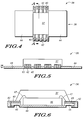
- FIG. 4 is a top view of an overmolded semiconductor device on a thermally conductive flexible substrate with edge half-vias and a pair of thermally conductive extensions in accordance with the present invention.
- FIG. 5 is a end view of the semiconductor device of FIG. 4.
- FIG. 6 is a cross-sectional view along line A-A of the overmolded semiconductor device of FIG. 4.
- FIG. 7 is a cross-sectional view of a plurality of the overmolded semiconductor device of FIG.4 stacked in a carrier socket, illustrating another embodiment of the present invention.
- FIG. 8 is a cross-sectional view of a plurality of the overmolded semiconductor device of FIG. 4 stacked in a carrier socket with spring contacts for chip enable, illustrating yet another embodiment of the present invention.
- FIG. 9 is an end view of the carrier socket and stacked semiconductor devices as illustrated in FIG. 7
- FIG. 10 is a partial top view of the carrier socket of FIG. 7 showing a plurality of spring contacts fitting into the edge half-vias of the overmolded semiconductor device of FIG. 4.
- FIG. 1 An oblique view of a stacked three dimensional leadless semiconductor multiple chip module 10 comprising two semiconductor devices 11 each having a package body 12 on a PCB substrate 14 is illustrated in FIG. 1, a first embodiment of the present invention.
- the package body 12 can be of but not limited to any conventional encapsulating material, for example, an epoxy resin-based molding compound.
- Package body 12 can be formed either through overmolding or through a "glob top” process. Overmolding can be accomplished in a transfer mold, which is a common tool in the art.
- a "glob top” process is where an encapsulant is either dispensed or melted over a semiconductor die to cover it.
- PCB substrate 14 has a plurality of metal conductors 16 extending past package body 12. Metal conductors 16 also extend to the bottom surface of PCB substrate 14.
- the advantage of semiconductor device 11 over conventional leaded packages is that the problem of lead damage is eliminated because metal conductors 16 perform substantially the same function as the external leads of conventional semiconductor packages, but metal conductors 16 are supported by a PCB substrate 14.
- Semiconductor device 11 can be tested and burned-in with a socket that makes contact with the plurality of metal conductors 16.
- metal conductors 16 have semi-circular edges to form a plurality of half-vias 18 along the edges of PCB substrate 14 giving the edges a castellated appearance.
- the plurality of half-vias 18 enables electrical interconnections between multiple semiconductor devices 11 to form a multiple chip module.
- Also illustrated in FIG. 1 is a plurality of electrical conductors 22 that connect the two semiconductor devices 11.
- Electrical conductors 22 can be either solder plated wires or solder filled springs.
- a solder filled spring is basically a spring filled with solder that looks substantially like a solid column of solder. During solder reflow when the solder is melted, the coils of the spring prevent the solder from collapsing because the molten solder will wet to the spring due to surface tension.
- each semiconductor device 11 has a semiconductor die 24 directly mounted to PCB substrate 14.
- Each semiconductor die 24 is electrically connected to the plurality of metal conductors 16 by way of a plurality of wire bonds 26 as illustrated in FIG. 2.
- the wires are bonded selectively to the plurality of metal conductors 16 so that each device in the stack is not identical. This differentiation is needed for chip enable requirements in the module. In some cases, the chip enable for each device is interconnected, but in that instance, the data outputs per device cannot be interconnected. Thus, it should be apparent that each device in the stack have to be marked accordingly because of the different wire bonding scheme of each device.
- the PCB substrates 14 are positioned such that the plurality of half-vias 18 of both semiconductor devices 11 are aligned to each other in the X-Y direction.
- the plurality of electrical conductors 22 fit into the plurality of half-vias 18 and are soldered thereto to electrically interconnect the semiconductor devices 11. Since each semiconductor device 11 is not identical in the wire bonding scheme, at least one of the plurality of electrical conductors 22 is unique per device. This uniqueness allows each device 11 to be selected during the multiple chip module's operation.
- the lower ends of the plurality of electrical conductors 22 are bent to enable the semiconductor multiple chip module 20 to be surface mounted to a PC board (not shown).
- FIG. 2 illustrates the plurality of electrical conductors 22 being bent outward, it is possible to bend the plurality of electrical conductors 22 inward and still enable surface mounting.
- FIG. 3 illustrates a second embodiment of the present invention.
- Semiconductor multiple chip module 27 has the same type of components as the module 10 of FIG. 2, and are thus labeled accordingly. The difference with the multiple chip module 27 is that the plurality of electrical conductors 22 are left straight to make the module 27 a through-hole type of module, as opposed to the surface mounting configuration of module 10 of FIG. 2.
- chip enable is offered if each device in the multiple chip module stack is desired to be wire bonded and marked identically.
- the chip enable connection for each device can be sheathed with an electrical insulator in such a manner that no electrical contact is made with the other device.
- chip enable for each device can be achieved.
- FIG. 4 Illustrated in FIG. 4 is a top view of a semiconductor device 36 that has an overmolded package body 37 on a flexible substrate 38, in accordance with the present invention.
- the overmolded package body 37 can be of but not limited to any conventional encapsulating material, for example, an epoxy resin-based molding compound.
- Flexible substrate 38 has a plurality of metal conductors 40 on two opposing sides extending past the package body 37 to the edges of flexible substrate 38.
- Metal conductors 40 are semi-circular in shape at the edges of the flexible substrate 38 to form a plurality of half-vias 42, giving those edges of the flexible substrate 38 a castellated appearance.
- metal conductors 40 also extend from the top surface of flexible substrate 38 to the bottom surface of flexible substrate 38.
- the plurality of half-vias 42 enables electrical interconnections between multiple semiconductor devices 36. Each semiconductor device 36 may be tested and burned-in individually.
- FIG. 4 is a pair of thermally conductive extensions 44 which is an integral part of the flexible substrate 38.
- FIG. 5 is an end view of the semiconductor device 36 further illustrating the pair of thermally conductive extensions 44.
- the thermally conductive extensions 44 are actually continuous under the package body 37.
- a thermally conductive material such as copper can be used for these extensions.
- the metal conductors 42 need to be electrically isolated from this continuous pair of extensions.
- FIG. 6. is a cross-sectional view along line A-A of FIG. 4, illustrating how the continuous pair of thermal extensions 44 can be isolated from the metal conductors 40.
- a layer of electrical insulator 45 is placed between the metal conductors 40 and the continuous pair of thermal extensions 44.
- FIG. 7 illustrates another embodiment of the present invention showing a multiple chip module 50 composed of two semiconductor devices 36 of FIG. 4.
- the two devices 36 each having a semiconductor die 46 electrically coupled to the flexible substrate 38 with a plurality of wire bonds 47, are stacked above one another in a carrier socket 56 that is electrically nonconductive.
- Carrier socket 56 can be molded from a thermally conductive molding compound, for example, an aluminum nitride filled molding compound.
- carrier socket 56 has a plurality of spring contacts 58 which are electrical conductors to electrically interconnect the semiconductor devices 36.
- the plurality of spring contacts 58 is pre-molded into carrier socket 56.
- the two semiconductor devices 36 are self-aligning in carrier socket 56 because of the plurality of half-vias 42 formed by the metal conductors 40.
- the plurality of spring contacts 58 fits into the plurality of half-vias and is soldered into place, or an external clip (not shown) can be used to hold the spring contacts 58 in contact with the metal conductors 40.
- the multiple chip module 50 can be surface mounted to a PC board (not shown). It should be understood that each semiconductor device in the stack must be wire bonded differently and marked accordingly for either chip enable requirements or for separating data outputs per device.
- FIG. 8 illustrates an embodiment of the present invention which allows a different chip enable scheme.
- a semiconductor multiple chip module 60 has substantially the same components as module 50 of FIG.7, thus, the components are labeled the same where appropriate.
- a plurality of spring contacts (not fully shown) electrically interconnect the semiconductor devices 36.
- One spring contact 61 makes a physical and electrical connection with only the upper device, while another spring contact 62 makes a physical and electrical contact with only the lower device. This configuration allows spring contacts 61 and 62 to be used for chip enable. The remaining spring contacts connect to both the upper and lower semiconductor devices.
- FIG. 9 illustrates an end view of the multiple chip module 50.
- the end view for the multiple chip module 60 of FIG. 8 will look substantially the same.
- the pairs of thermally conductive extensions 44 are shown to touch the inner sidewalls of carrier socket 56.
- the flexibility of substrate 38 enables the pair of thermally conductive extensions 44 to be bent in such a manner.
- This configurations serves two purposes, the first one being an enhancement in the heat dissipation of the module 50.
- the bending of the pairs of thermally conductive extensions 44 also help to hold each semiconductor device 36 in carrier socket 56 before the plurality of spring contacts 58 are soldered into place, due to the outward force that the extensions 44 exert on the sidewalls of carrier socket 56.
- FIG. 10 Illustrated in FIG. 10 is a partial top view 64 of carrier socket 56 with the plurality of spring contacts 58, further illustrating the method for stacking multiple semiconductor devices in a carrier socket 56 using the plurality of half-vias 42 as the self-aligning feature.
- the inner sidewalls of carrier socket 56 that contain the plurality of spring contacts 58 are castellated to prevent the plurality of spring contacts 58 from bending and shifting positions inside the socket 56.
- the plurality of spring contacts 58 fits into the plurality of half-vias 42 of the semiconductor device as each device is pushed inside carrier socket 56.
- the locations of the plurality of spring contacts 58 and the plurality of half-vias 42 ensure that each semiconductor device is properly self-aligned in the carrier socket 56.
- the foregoing description and illustrations contained herein demonstrate many of the advantages associated with the present invention.
- the invention enables three dimensional multiple chip module that can be surface mounted to a PC board.
- Three dimensional packaging offers higher memory density and less required interconnect density than planar multiple chip substrates.
- the configuration of this three dimensional stacked leadless multiple chip module is self-aligning.
- the plurality of half-vias along the castellated edges of the substrate enables the simple stacking of semiconductor devices.
- the fact that each substrate can be directly stacked on top of another device without any additional layers helps to minimize the overall height of the multiple chip module.
- the plurality of electrical conductors also aid in the heat dissipation of the module.
Abstract
Description
From U.S Patent 4,956,694 there is know a method of stacking two ceramic leadless chip carriers (LCCs) which are soldered together and are held together solely by solder; the stacked module of LCCs are further soldered to a single substrate and must be soldered to an additional substrate for mounting to a board.
From Research Disclosure, No. 313, May 1990, EMSWORTH, GB, Page 372,
Claims (9)
- A semiconductor device comprising:a semiconductor die (46);a thermally conductive substrate (38) attached to the semiconductor die (46) having a first set of opposing edges and a second set of opposing edges;a layer of insulator (45) overlying portions of the thermally conductive substrate (38); andmetal conductors (40) lying on the layer of insulator (45), wherein the metal conductors (40) lie along the first set of opposing edges but do not lie along the second set of opposing edges.
- A semiconductor multi-chip module (50) comprising:a first semiconductor device and a second semiconductor device each including:a semiconductor die (46);a thermally conductive substrate (38) attached to the semiconductor die (46) having a first set of opposing edges including a first edge and a second edge and a second set of opposing edges;a layer of insulator (45) overlying portions of the thermally conductive substrate (38); andmetal conductors (40) lying on the layer of insulator (45), wherein the metal conductors (40) lie along the first set of opposing edges but do not lie along the second set of opposing edges;electrical conductors (58) including a first electrical conductor and a second electrical conductor, wherein:the first electrical conductor contacts metal conductors lying along the first edges of the first and second semiconductor devices; andthe second electrical conductor contacts metal conductors lying along the second edges of the first and second semiconductor devices.
- The semiconductor multi-chip module, further characterised by a carrier socket (56), wherein the first and second electrical conductors (58) are attached to the carrier socket (56).
- The semiconductor device of claim 1 or the semiconductor multi-chip module of claim 2 or 3, characterised such that the thermally conductive substrate is metallic.
- The semiconductor device of claim 1 or the semiconductor multi-chip module of claim 2 or 3, characterised such that the thermally conductive substrate includes copper.
- The semiconductor device of claim 1 or the semiconductor multi-chip module of claim 2, 3, 4, 5, or 6, characterised such that the metallic conductors have shapes that define half-vias.
- The semiconductor multi-chip module of claim 6, characterised such that the first and second electrical conductors are spring contacts.
- The semiconductor device of claim 1 or the semiconductor multi-chip module of claim 2, 3, 4, 5, 6, or 7, further characterised by a resin-based compound overlying the semiconductor die and a portion of the thermally conductive substrate.
- The semiconductor multi-chip module of claim 2, 3, 4, 5, 6, 7, or 8, characterised such that the electrical conductors further include a third electrical conductor and a fourth electrical conductor, wherein:the third electrical conductor is electrically connected to the first semiconductor die but is not electrically connected to the second semiconductor die, andthe fourth electrical conductor is electrically connected to the second semiconductor die but is not electrically connected to the first semiconductor die.
Applications Claiming Priority (3)
| Application Number | Priority Date | Filing Date | Title |
|---|---|---|---|
| US07/887,963 US5247423A (en) | 1992-05-26 | 1992-05-26 | Stacking three dimensional leadless multi-chip module and method for making the same |
| US887963 | 1992-05-26 | ||
| EP93105802A EP0571749A1 (en) | 1992-05-26 | 1993-04-08 | Stacking semiconductor multi-chip module and method for making the same |
Related Parent Applications (1)
| Application Number | Title | Priority Date | Filing Date |
|---|---|---|---|
| EP93105802.8 Division | 1993-04-08 |
Publications (2)
| Publication Number | Publication Date |
|---|---|
| EP0862217A2 true EP0862217A2 (en) | 1998-09-02 |
| EP0862217A3 EP0862217A3 (en) | 1999-12-15 |
Family
ID=25392232
Family Applications (2)
| Application Number | Title | Priority Date | Filing Date |
|---|---|---|---|
| EP93105802A Withdrawn EP0571749A1 (en) | 1992-05-26 | 1993-04-08 | Stacking semiconductor multi-chip module and method for making the same |
| EP98106232A Withdrawn EP0862217A3 (en) | 1992-05-26 | 1993-04-08 | Semiconductor device and semiconductor multi-chip module |
Family Applications Before (1)
| Application Number | Title | Priority Date | Filing Date |
|---|---|---|---|
| EP93105802A Withdrawn EP0571749A1 (en) | 1992-05-26 | 1993-04-08 | Stacking semiconductor multi-chip module and method for making the same |
Country Status (4)
| Country | Link |
|---|---|
| US (1) | US5247423A (en) |
| EP (2) | EP0571749A1 (en) |
| JP (1) | JPH0637248A (en) |
| KR (1) | KR930024134A (en) |
Cited By (1)
| Publication number | Priority date | Publication date | Assignee | Title |
|---|---|---|---|---|
| WO2007058988A1 (en) * | 2005-11-16 | 2007-05-24 | Sandisk Corporation | Padless substrate for surface mounted components |
Families Citing this family (179)
| Publication number | Priority date | Publication date | Assignee | Title |
|---|---|---|---|---|
| WO1992003035A1 (en) * | 1990-08-01 | 1992-02-20 | Staktek Corporation | Ultra high density integrated circuit packages, method and apparatus |
| US5446620A (en) * | 1990-08-01 | 1995-08-29 | Staktek Corporation | Ultra high density integrated circuit packages |
| FR2688629A1 (en) * | 1992-03-10 | 1993-09-17 | Thomson Csf | Method and device for three-dimensional encapsulation of semiconductor chips |
| US5412159A (en) * | 1993-09-27 | 1995-05-02 | Zenith Electronics Corporation | High voltage resistive network circuit board with good potting adhesion |
| EP0658937A1 (en) * | 1993-12-08 | 1995-06-21 | Hughes Aircraft Company | Vertical IC chip stack with discrete chip carriers formed from dielectric tape |
| US5544174A (en) * | 1994-03-17 | 1996-08-06 | The United States Of America As Represented By The Secretary Of The Air Force | Programmable boundary scan and input output parameter device for testing integrated circuits |
| US5891761A (en) * | 1994-06-23 | 1999-04-06 | Cubic Memory, Inc. | Method for forming vertical interconnect process for silicon segments with thermally conductive epoxy preform |
| US5698895A (en) * | 1994-06-23 | 1997-12-16 | Cubic Memory, Inc. | Silicon segment programming method and apparatus |
| US6486528B1 (en) | 1994-06-23 | 2002-11-26 | Vertical Circuits, Inc. | Silicon segment programming apparatus and three terminal fuse configuration |
| US6080596A (en) * | 1994-06-23 | 2000-06-27 | Cubic Memory Inc. | Method for forming vertical interconnect process for silicon segments with dielectric isolation |
| US5675180A (en) * | 1994-06-23 | 1997-10-07 | Cubic Memory, Inc. | Vertical interconnect process for silicon segments |
| US6255726B1 (en) | 1994-06-23 | 2001-07-03 | Cubic Memory, Inc. | Vertical interconnect process for silicon segments with dielectric isolation |
| US5657206A (en) * | 1994-06-23 | 1997-08-12 | Cubic Memory, Inc. | Conductive epoxy flip-chip package and method |
| US6124633A (en) * | 1994-06-23 | 2000-09-26 | Cubic Memory | Vertical interconnect process for silicon segments with thermally conductive epoxy preform |
| US5434745A (en) * | 1994-07-26 | 1995-07-18 | White Microelectronics Div. Of Bowmar Instrument Corp. | Stacked silicon die carrier assembly |
| US5671121A (en) * | 1994-09-29 | 1997-09-23 | Intel Corporation | Kangaroo multi-package interconnection concept |
| US5696030A (en) * | 1994-09-30 | 1997-12-09 | International Business Machines Corporation | Integrated circuit contacts having improved electromigration characteristics and fabrication methods therefor |
| US5715144A (en) * | 1994-12-30 | 1998-02-03 | International Business Machines Corporation | Multi-layer, multi-chip pyramid and circuit board structure |
| JP2944449B2 (en) * | 1995-02-24 | 1999-09-06 | 日本電気株式会社 | Semiconductor package and manufacturing method thereof |
| KR0148082B1 (en) * | 1995-08-16 | 1998-08-01 | 김광호 | Stack semiconductor package and package socket |
| US6025642A (en) * | 1995-08-17 | 2000-02-15 | Staktek Corporation | Ultra high density integrated circuit packages |
| JPH0969587A (en) * | 1995-08-30 | 1997-03-11 | Nec Kyushu Ltd | Bga type semiconductor device and bga module |
| US5861666A (en) * | 1995-08-30 | 1999-01-19 | Tessera, Inc. | Stacked chip assembly |
| US5623160A (en) * | 1995-09-14 | 1997-04-22 | Liberkowski; Janusz B. | Signal-routing or interconnect substrate, structure and apparatus |
| US5661337A (en) * | 1995-11-07 | 1997-08-26 | Vlsi Technology, Inc. | Technique for improving bonding strength of leadframe to substrate in semiconductor IC chip packages |
| KR100192180B1 (en) * | 1996-03-06 | 1999-06-15 | 김영환 | Buttom lead package of multi layer |
| KR100192179B1 (en) * | 1996-03-06 | 1999-06-15 | 김영환 | Semiconductor package |
| US5956601A (en) * | 1996-04-25 | 1999-09-21 | Kabushiki Kaisha Toshiba | Method of mounting a plurality of semiconductor devices in corresponding supporters |
| US5907903A (en) * | 1996-05-24 | 1999-06-01 | International Business Machines Corporation | Multi-layer-multi-chip pyramid and circuit board structure and method of forming same |
| DE19626126C2 (en) * | 1996-06-28 | 1998-04-16 | Fraunhofer Ges Forschung | Method for forming a spatial chip arrangement and spatial chip arrangement |
| US5748452A (en) * | 1996-07-23 | 1998-05-05 | International Business Machines Corporation | Multi-electronic device package |
| DE19638175C2 (en) | 1996-09-18 | 2000-05-25 | Siemens Ag | Integrated circuit (chip) with a housing and external configuration option |
| KR100239703B1 (en) * | 1996-10-21 | 2000-01-15 | 김영환 | Three dimension semiconductor package and fabrication method thereof |
| US7149095B2 (en) * | 1996-12-13 | 2006-12-12 | Tessera, Inc. | Stacked microelectronic assemblies |
| US6225688B1 (en) | 1997-12-11 | 2001-05-01 | Tessera, Inc. | Stacked microelectronic assembly and method therefor |
| US6121676A (en) * | 1996-12-13 | 2000-09-19 | Tessera, Inc. | Stacked microelectronic assembly and method therefor |
| JP2964983B2 (en) * | 1997-04-02 | 1999-10-18 | 日本電気株式会社 | Three-dimensional memory module and semiconductor device using the same |
| KR100422608B1 (en) * | 1997-05-10 | 2004-06-04 | 삼성전자주식회사 | Stack chip package |
| KR100266637B1 (en) * | 1997-11-15 | 2000-09-15 | 김영환 | Stackable ball grid array semiconductor package and a method thereof |
| US6034441A (en) * | 1997-11-26 | 2000-03-07 | Lucent Technologies, Inc. | Overcast semiconductor package |
| US5956233A (en) * | 1997-12-19 | 1999-09-21 | Texas Instruments Incorporated | High density single inline memory module |
| RU2176134C2 (en) * | 1998-07-02 | 2001-11-20 | Закрытое акционерное общество "Техно-ТМ" | Three-dimensional electron module and process of its manufacture |
| KR100302593B1 (en) * | 1998-10-24 | 2001-09-22 | 김영환 | Semiconductor package and fabricating method thereof |
| FR2785722A1 (en) * | 1998-11-06 | 2000-05-12 | Bull Sa | THREE-DIMENSIONAL INTERCONNECTION STRUCTURE OF MULTIPLE CIRCUITS TO FORM A MULTI-COMPONENT PACKAGE |
| KR20000050605A (en) * | 1999-01-12 | 2000-08-05 | 박천주 | Solderless and Wireless Socket-type Circuit Board pressed and adhered with multi-layered conductible circuit panel |
| US6323060B1 (en) | 1999-05-05 | 2001-11-27 | Dense-Pac Microsystems, Inc. | Stackable flex circuit IC package and method of making same |
| US6890798B2 (en) | 1999-06-08 | 2005-05-10 | Intel Corporation | Stacked chip packaging |
| US6617671B1 (en) | 1999-06-10 | 2003-09-09 | Micron Technology, Inc. | High density stackable and flexible substrate-based semiconductor device modules |
| US6278181B1 (en) | 1999-06-28 | 2001-08-21 | Advanced Micro Devices, Inc. | Stacked multi-chip modules using C4 interconnect technology having improved thermal management |
| US6249136B1 (en) | 1999-06-28 | 2001-06-19 | Advanced Micro Devices, Inc. | Bottom side C4 bumps for integrated circuits |
| US6572387B2 (en) | 1999-09-24 | 2003-06-03 | Staktek Group, L.P. | Flexible circuit connector for stacked chip module |
| WO2001026432A1 (en) | 1999-10-01 | 2001-04-12 | Seiko Epson Corporation | Wiring board, semiconductor device and method of producing, testing and packaging the same, and circuit board and electronic equipment |
| US6621155B1 (en) | 1999-12-23 | 2003-09-16 | Rambus Inc. | Integrated circuit device having stacked dies and impedance balanced transmission lines |
| US6262895B1 (en) | 2000-01-13 | 2001-07-17 | John A. Forthun | Stackable chip package with flex carrier |
| US6631555B1 (en) * | 2000-02-08 | 2003-10-14 | Cardiac Pacemakers, Inc. | Method of thin film deposition as an active conductor |
| KR100675728B1 (en) * | 2000-03-16 | 2007-02-01 | 삼성전자주식회사 | Stack chip package |
| US6236565B1 (en) * | 2000-06-15 | 2001-05-22 | Mark G. Gordon | Chip stack with active cooling system |
| EP1318546A4 (en) * | 2000-07-19 | 2007-08-08 | Shindo Company Ltd | Semiconductor device |
| US6608763B1 (en) | 2000-09-15 | 2003-08-19 | Staktek Group L.P. | Stacking system and method |
| US6885106B1 (en) | 2001-01-11 | 2005-04-26 | Tessera, Inc. | Stacked microelectronic assemblies and methods of making same |
| US20020127771A1 (en) * | 2001-03-12 | 2002-09-12 | Salman Akram | Multiple die package |
| SG95637A1 (en) * | 2001-03-15 | 2003-04-23 | Micron Technology Inc | Semiconductor/printed circuit board assembly, and computer system |
| US6462408B1 (en) | 2001-03-27 | 2002-10-08 | Staktek Group, L.P. | Contact member stacking system and method |
| US6441483B1 (en) * | 2001-03-30 | 2002-08-27 | Micron Technology, Inc. | Die stacking scheme |
| KR20010086476A (en) * | 2001-07-13 | 2001-09-13 | 신이술 | Printed circuit board and package method of stacking semiconductor using therof |
| DE10134648A1 (en) * | 2001-07-20 | 2002-10-10 | Infineon Technologies Ag | Stacked electronic component device has perpendicular pins providing mechanical and electrical connections between stacked electronic components |
| US7218527B1 (en) * | 2001-08-17 | 2007-05-15 | Alien Technology Corporation | Apparatuses and methods for forming smart labels |
| US20030048624A1 (en) * | 2001-08-22 | 2003-03-13 | Tessera, Inc. | Low-height multi-component assemblies |
| US6734370B2 (en) * | 2001-09-07 | 2004-05-11 | Irvine Sensors Corporation | Multilayer modules with flexible substrates |
| US6977440B2 (en) * | 2001-10-09 | 2005-12-20 | Tessera, Inc. | Stacked packages |
| AU2002337834A1 (en) * | 2001-10-09 | 2003-04-22 | Tessera, Inc. | Stacked packages |
| US7335995B2 (en) | 2001-10-09 | 2008-02-26 | Tessera, Inc. | Microelectronic assembly having array including passive elements and interconnects |
| US7485951B2 (en) | 2001-10-26 | 2009-02-03 | Entorian Technologies, Lp | Modularized die stacking system and method |
| US7656678B2 (en) | 2001-10-26 | 2010-02-02 | Entorian Technologies, Lp | Stacked module systems |
| US6956284B2 (en) * | 2001-10-26 | 2005-10-18 | Staktek Group L.P. | Integrated circuit stacking system and method |
| US7026708B2 (en) | 2001-10-26 | 2006-04-11 | Staktek Group L.P. | Low profile chip scale stacking system and method |
| US20060255446A1 (en) | 2001-10-26 | 2006-11-16 | Staktek Group, L.P. | Stacked modules and method |
| US20030234443A1 (en) | 2001-10-26 | 2003-12-25 | Staktek Group, L.P. | Low profile stacking system and method |
| US6940729B2 (en) | 2001-10-26 | 2005-09-06 | Staktek Group L.P. | Integrated circuit stacking system and method |
| US6914324B2 (en) | 2001-10-26 | 2005-07-05 | Staktek Group L.P. | Memory expansion and chip scale stacking system and method |
| US6576992B1 (en) | 2001-10-26 | 2003-06-10 | Staktek Group L.P. | Chip scale stacking system and method |
| US7310458B2 (en) | 2001-10-26 | 2007-12-18 | Staktek Group L.P. | Stacked module systems and methods |
| US7053478B2 (en) | 2001-10-26 | 2006-05-30 | Staktek Group L.P. | Pitch change and chip scale stacking system |
| US7371609B2 (en) | 2001-10-26 | 2008-05-13 | Staktek Group L.P. | Stacked module systems and methods |
| US7202555B2 (en) | 2001-10-26 | 2007-04-10 | Staktek Group L.P. | Pitch change and chip scale stacking system and method |
| US7081373B2 (en) | 2001-12-14 | 2006-07-25 | Staktek Group, L.P. | CSP chip stack with flex circuit |
| US20030131472A1 (en) * | 2002-01-15 | 2003-07-17 | Mitac International Corp. | Method of fabricating a multi-layer circuit board assembly |
| JP2003318361A (en) * | 2002-04-19 | 2003-11-07 | Fujitsu Ltd | Semiconductor device and method of manufacturing the same |
| US20050167817A1 (en) * | 2002-08-05 | 2005-08-04 | Tessera, Inc. | Microelectronic adaptors, assemblies and methods |
| US6765288B2 (en) | 2002-08-05 | 2004-07-20 | Tessera, Inc. | Microelectronic adaptors, assemblies and methods |
| WO2004017399A1 (en) * | 2002-08-16 | 2004-02-26 | Tessera, Inc. | Microelectronic packages with self-aligning features |
| US7294928B2 (en) * | 2002-09-06 | 2007-11-13 | Tessera, Inc. | Components, methods and assemblies for stacked packages |
| US7071547B2 (en) * | 2002-09-11 | 2006-07-04 | Tessera, Inc. | Assemblies having stacked semiconductor chips and methods of making same |
| US7064426B2 (en) * | 2002-09-17 | 2006-06-20 | Chippac, Inc. | Semiconductor multi-package module having wire bond interconnect between stacked packages |
| JP4800625B2 (en) * | 2002-09-17 | 2011-10-26 | スタッツ・チップパック・インコーポレイテッド | Semiconductor multi-package module having wire bond interconnection between stacked packages and method of forming the same |
| US7205647B2 (en) * | 2002-09-17 | 2007-04-17 | Chippac, Inc. | Semiconductor multi-package module having package stacked over ball grid array package and having wire bond interconnect between stacked packages |
| US20040061213A1 (en) * | 2002-09-17 | 2004-04-01 | Chippac, Inc. | Semiconductor multi-package module having package stacked over die-up flip chip ball grid array package and having wire bond interconnect between stacked packages |
| US7061122B2 (en) * | 2002-10-11 | 2006-06-13 | Tessera, Inc. | Components, methods and assemblies for multi-chip packages |
| US6841029B2 (en) * | 2003-03-27 | 2005-01-11 | Advanced Cardiovascular Systems, Inc. | Surface modification of expanded ultra high molecular weight polyethylene (eUHMWPE) for improved bondability |
| US7542304B2 (en) | 2003-09-15 | 2009-06-02 | Entorian Technologies, Lp | Memory expansion and integrated circuit stacking system and method |
| US8641913B2 (en) * | 2003-10-06 | 2014-02-04 | Tessera, Inc. | Fine pitch microcontacts and method for forming thereof |
| US7495179B2 (en) | 2003-10-06 | 2009-02-24 | Tessera, Inc. | Components with posts and pads |
| US7061121B2 (en) | 2003-11-12 | 2006-06-13 | Tessera, Inc. | Stacked microelectronic assemblies with central contacts |
| US7134194B2 (en) * | 2003-11-13 | 2006-11-14 | Delphi Technologies, Inc. | Method of developing an electronic module |
| US7709968B2 (en) * | 2003-12-30 | 2010-05-04 | Tessera, Inc. | Micro pin grid array with pin motion isolation |
| CN100343964C (en) * | 2004-02-13 | 2007-10-17 | 旺宏电子股份有限公司 | Multiple chip packaging arrangement |
| US7705432B2 (en) * | 2004-04-13 | 2010-04-27 | Vertical Circuits, Inc. | Three dimensional six surface conformal die coating |
| US7215018B2 (en) * | 2004-04-13 | 2007-05-08 | Vertical Circuits, Inc. | Stacked die BGA or LGA component assembly |
| US7245021B2 (en) * | 2004-04-13 | 2007-07-17 | Vertical Circuits, Inc. | Micropede stacked die component assembly |
| US7217597B2 (en) | 2004-06-22 | 2007-05-15 | Micron Technology, Inc. | Die stacking scheme |
| US7507914B2 (en) * | 2004-06-30 | 2009-03-24 | Honeywell International Inc. | Micro-castellated interposer |
| US7760513B2 (en) | 2004-09-03 | 2010-07-20 | Entorian Technologies Lp | Modified core for circuit module system and method |
| US7446410B2 (en) | 2004-09-03 | 2008-11-04 | Entorian Technologies, Lp | Circuit module with thermal casing systems |
| US7289327B2 (en) | 2006-02-27 | 2007-10-30 | Stakick Group L.P. | Active cooling methods and apparatus for modules |
| US7443023B2 (en) | 2004-09-03 | 2008-10-28 | Entorian Technologies, Lp | High capacity thin module system |
| US7511968B2 (en) | 2004-09-03 | 2009-03-31 | Entorian Technologies, Lp | Buffered thin module system and method |
| US7606049B2 (en) | 2004-09-03 | 2009-10-20 | Entorian Technologies, Lp | Module thermal management system and method |
| US7606040B2 (en) | 2004-09-03 | 2009-10-20 | Entorian Technologies, Lp | Memory module system and method |
| US7616452B2 (en) | 2004-09-03 | 2009-11-10 | Entorian Technologies, Lp | Flex circuit constructions for high capacity circuit module systems and methods |
| US7468893B2 (en) | 2004-09-03 | 2008-12-23 | Entorian Technologies, Lp | Thin module system and method |
| US7522421B2 (en) | 2004-09-03 | 2009-04-21 | Entorian Technologies, Lp | Split core circuit module |
| US7579687B2 (en) | 2004-09-03 | 2009-08-25 | Entorian Technologies, Lp | Circuit module turbulence enhancement systems and methods |
| US20060050492A1 (en) | 2004-09-03 | 2006-03-09 | Staktek Group, L.P. | Thin module system and method |
| US7423885B2 (en) | 2004-09-03 | 2008-09-09 | Entorian Technologies, Lp | Die module system |
| US7324352B2 (en) | 2004-09-03 | 2008-01-29 | Staktek Group L.P. | High capacity thin module system and method |
| US7542297B2 (en) | 2004-09-03 | 2009-06-02 | Entorian Technologies, Lp | Optimized mounting area circuit module system and method |
| US7606050B2 (en) | 2004-09-03 | 2009-10-20 | Entorian Technologies, Lp | Compact module system and method |
| DE102004044882B3 (en) * | 2004-09-14 | 2006-04-20 | Infineon Technologies Ag | Semiconductor module having stacked semiconductor devices and electrical interconnects between the stacked semiconductor devices |
| KR100658734B1 (en) * | 2004-11-11 | 2006-12-19 | 주식회사 유니세미콘 | A stack semiconductor package and its manufacture method |
| US7483561B2 (en) | 2004-11-30 | 2009-01-27 | Psion Teklogix Systems Inc. | Miniaturized imaging module construction technique |
| US7309914B2 (en) | 2005-01-20 | 2007-12-18 | Staktek Group L.P. | Inverted CSP stacking system and method |
| US7196427B2 (en) * | 2005-04-18 | 2007-03-27 | Freescale Semiconductor, Inc. | Structure having an integrated circuit on another integrated circuit with an intervening bent adhesive element |
| US7098073B1 (en) | 2005-04-18 | 2006-08-29 | Freescale Semiconductor, Inc. | Method for stacking an integrated circuit on another integrated circuit |
| US7033861B1 (en) | 2005-05-18 | 2006-04-25 | Staktek Group L.P. | Stacked module systems and method |
| US7576995B2 (en) | 2005-11-04 | 2009-08-18 | Entorian Technologies, Lp | Flex circuit apparatus and method for adding capacitance while conserving circuit board surface area |
| US7323968B2 (en) * | 2005-12-09 | 2008-01-29 | Sony Corporation | Cross-phase adapter for powerline communications (PLC) network |
| US7608920B2 (en) | 2006-01-11 | 2009-10-27 | Entorian Technologies, Lp | Memory card and method for devising |
| US7605454B2 (en) | 2006-01-11 | 2009-10-20 | Entorian Technologies, Lp | Memory card and method for devising |
| US7508058B2 (en) | 2006-01-11 | 2009-03-24 | Entorian Technologies, Lp | Stacked integrated circuit module |
| US7304382B2 (en) | 2006-01-11 | 2007-12-04 | Staktek Group L.P. | Managed memory component |
| US7508069B2 (en) | 2006-01-11 | 2009-03-24 | Entorian Technologies, Lp | Managed memory component |
| US7511969B2 (en) | 2006-02-02 | 2009-03-31 | Entorian Technologies, Lp | Composite core circuit module system and method |
| US7732907B2 (en) * | 2006-05-30 | 2010-06-08 | Stats Chippac Ltd. | Integrated circuit package system with edge connection system |
| KR100817054B1 (en) | 2006-07-13 | 2008-03-26 | 삼성전자주식회사 | A socket for testing packages, a rubber for the test socket, and a guide for the test socket |
| US7638868B2 (en) * | 2006-08-16 | 2009-12-29 | Tessera, Inc. | Microelectronic package |
| US7545029B2 (en) | 2006-08-18 | 2009-06-09 | Tessera, Inc. | Stack microelectronic assemblies |
| US7468553B2 (en) | 2006-10-20 | 2008-12-23 | Entorian Technologies, Lp | Stackable micropackages and stacked modules |
| US7417310B2 (en) | 2006-11-02 | 2008-08-26 | Entorian Technologies, Lp | Circuit module having force resistant construction |
| KR101330731B1 (en) * | 2007-02-08 | 2013-11-20 | 삼성전자주식회사 | Image forming apparatus |
| DE102007032142A1 (en) * | 2007-06-30 | 2009-01-02 | Robert Bosch Gmbh | Electronic module and method for producing an electronic module |
| US7763983B2 (en) * | 2007-07-02 | 2010-07-27 | Tessera, Inc. | Stackable microelectronic device carriers, stacked device carriers and methods of making the same |
| US7906838B2 (en) * | 2007-07-23 | 2011-03-15 | Headway Technologies, Inc. | Electronic component package and method of manufacturing same |
| US8299626B2 (en) | 2007-08-16 | 2012-10-30 | Tessera, Inc. | Microelectronic package |
| US8558379B2 (en) | 2007-09-28 | 2013-10-15 | Tessera, Inc. | Flip chip interconnection with double post |
| TW200931634A (en) | 2008-01-10 | 2009-07-16 | Abounion Technology Corp | Multi-channel stacked semiconductor device and method for fabricating the same, and stacking substrate applied to the semiconductor device |
| TWI399845B (en) * | 2009-09-24 | 2013-06-21 | Powertech Technology Inc | Multi-chip stacked device without loop height and its manufacturing method |
| US8330272B2 (en) | 2010-07-08 | 2012-12-11 | Tessera, Inc. | Microelectronic packages with dual or multiple-etched flip-chip connectors |
| US8580607B2 (en) | 2010-07-27 | 2013-11-12 | Tessera, Inc. | Microelectronic packages with nanoparticle joining |
| US8611090B2 (en) * | 2010-09-09 | 2013-12-17 | International Business Machines Corporation | Electronic module with laterally-conducting heat distributor layer |
| US8853558B2 (en) | 2010-12-10 | 2014-10-07 | Tessera, Inc. | Interconnect structure |
| US8966747B2 (en) | 2011-05-11 | 2015-03-03 | Vlt, Inc. | Method of forming an electrical contact |
| US8779585B2 (en) | 2011-08-05 | 2014-07-15 | International Business Machines Corporation | Implementing enhanced thermal conductivity in stacked modules |
| US8872318B2 (en) | 2011-08-24 | 2014-10-28 | Tessera, Inc. | Through interposer wire bond using low CTE interposer with coarse slot apertures |
| KR101772490B1 (en) | 2011-09-28 | 2017-08-30 | 삼성전자주식회사 | Printed circuit board assembly |
| USD680119S1 (en) * | 2011-11-15 | 2013-04-16 | Connectblue Ab | Module |
| USD689053S1 (en) * | 2011-11-15 | 2013-09-03 | Connectblue Ab | Module |
| USD680545S1 (en) * | 2011-11-15 | 2013-04-23 | Connectblue Ab | Module |
| USD692896S1 (en) * | 2011-11-15 | 2013-11-05 | Connectblue Ab | Module |
| US9070653B2 (en) * | 2013-01-15 | 2015-06-30 | Freescale Semiconductor, Inc. | Microelectronic assembly having a heat spreader for a plurality of die |
| US8698288B1 (en) * | 2013-05-23 | 2014-04-15 | Freescale Semiconductor, Inc. | Flexible substrate with crimping interconnection |
| US8884420B1 (en) * | 2013-07-12 | 2014-11-11 | Infineon Technologies Austria Ag | Multichip device |
| US9171742B2 (en) | 2013-07-22 | 2015-10-27 | Globalfoundries U.S. 2 Llc | Alignment of integrated circuit chip stack |
| CN103779286A (en) * | 2014-01-26 | 2014-05-07 | 清华大学 | Encapsulation structure, encapsulation method and template used in encapsulation method |
| US9633971B2 (en) | 2015-07-10 | 2017-04-25 | Invensas Corporation | Structures and methods for low temperature bonding using nanoparticles |
| US10886250B2 (en) | 2015-07-10 | 2021-01-05 | Invensas Corporation | Structures and methods for low temperature bonding using nanoparticles |
| JP2018147938A (en) * | 2017-03-01 | 2018-09-20 | 東芝メモリ株式会社 | Semiconductor device |
| KR102158785B1 (en) * | 2018-12-14 | 2020-09-22 | 국방과학연구소 | Laser diode bar structure and package of stacked laser diode bar |
| TWI706528B (en) * | 2019-08-08 | 2020-10-01 | 南茂科技股份有限公司 | Electronic package device |
| KR102398110B1 (en) * | 2020-08-13 | 2022-05-13 | 주식회사 경신 | In-cable controller of charger |
Citations (3)
| Publication number | Priority date | Publication date | Assignee | Title |
|---|---|---|---|---|
| FR2033678A5 (en) * | 1969-03-03 | 1970-12-04 | North American Rockwell | |
| EP0272390A2 (en) * | 1986-11-25 | 1988-06-29 | Kabushiki Kaisha Toshiba | Packages for a semiconductor device |
| US4956694A (en) * | 1988-11-04 | 1990-09-11 | Dense-Pac Microsystems, Inc. | Integrated circuit chip stacking |
Family Cites Families (9)
| Publication number | Priority date | Publication date | Assignee | Title |
|---|---|---|---|---|
| FR1439989A (en) * | 1965-04-02 | 1966-05-27 | Bull General Electric | Improvements to permanent memories with resistive couplings |
| US3304468A (en) * | 1965-05-05 | 1967-02-14 | Gen Electric | Replaceable electronic module for master circuit boards |
| US3588852A (en) * | 1967-12-26 | 1971-06-28 | Cambridge Memory Systems Inc | Memory assembly |
| JPS61101067A (en) * | 1984-10-24 | 1986-05-19 | Nec Corp | Memory module |
| US4862249A (en) * | 1987-04-17 | 1989-08-29 | Xoc Devices, Inc. | Packaging system for stacking integrated circuits |
| US5016138A (en) * | 1987-10-27 | 1991-05-14 | Woodman John K | Three dimensional integrated circuit package |
| WO1992003035A1 (en) * | 1990-08-01 | 1992-02-20 | Staktek Corporation | Ultra high density integrated circuit packages, method and apparatus |
| US5155661A (en) * | 1991-05-15 | 1992-10-13 | Hewlett-Packard Company | Aluminum nitride multi-chip module |
| US5162975A (en) * | 1991-10-15 | 1992-11-10 | Hewlett-Packard Company | Integrated circuit demountable TAB apparatus |
-
1992
- 1992-05-26 US US07/887,963 patent/US5247423A/en not_active Expired - Lifetime
-
1993
- 1993-04-08 EP EP93105802A patent/EP0571749A1/en not_active Withdrawn
- 1993-04-08 EP EP98106232A patent/EP0862217A3/en not_active Withdrawn
- 1993-05-13 KR KR1019930008183A patent/KR930024134A/en not_active Application Discontinuation
- 1993-05-21 JP JP5141266A patent/JPH0637248A/en active Pending
Patent Citations (3)
| Publication number | Priority date | Publication date | Assignee | Title |
|---|---|---|---|---|
| FR2033678A5 (en) * | 1969-03-03 | 1970-12-04 | North American Rockwell | |
| EP0272390A2 (en) * | 1986-11-25 | 1988-06-29 | Kabushiki Kaisha Toshiba | Packages for a semiconductor device |
| US4956694A (en) * | 1988-11-04 | 1990-09-11 | Dense-Pac Microsystems, Inc. | Integrated circuit chip stacking |
Non-Patent Citations (1)
| Title |
|---|
| PATENT ABSTRACTS OF JAPAN vol. 010, no. 283 (E-440), 26 September 1986 (1986-09-26) & JP 61 101067 A (NEC CORP), 19 May 1986 (1986-05-19) * |
Cited By (2)
| Publication number | Priority date | Publication date | Assignee | Title |
|---|---|---|---|---|
| WO2007058988A1 (en) * | 2005-11-16 | 2007-05-24 | Sandisk Corporation | Padless substrate for surface mounted components |
| US7967184B2 (en) | 2005-11-16 | 2011-06-28 | Sandisk Corporation | Padless substrate for surface mounted components |
Also Published As
| Publication number | Publication date |
|---|---|
| KR930024134A (en) | 1993-12-22 |
| JPH0637248A (en) | 1994-02-10 |
| EP0862217A3 (en) | 1999-12-15 |
| EP0571749A1 (en) | 1993-12-01 |
| US5247423A (en) | 1993-09-21 |
Similar Documents
| Publication | Publication Date | Title |
|---|---|---|
| US5247423A (en) | Stacking three dimensional leadless multi-chip module and method for making the same | |
| US7408255B2 (en) | Assembly for stacked BGA packages | |
| US5684330A (en) | Chip-sized package having metal circuit substrate | |
| US4616406A (en) | Process of making a semiconductor device having parallel leads directly connected perpendicular to integrated circuit layers therein | |
| KR100248678B1 (en) | Stackable three-dimensional multiple chip semiconductor device and method for making the same | |
| US6890798B2 (en) | Stacked chip packaging | |
| KR0184076B1 (en) | Three-dimensional stacked package | |
| US5777345A (en) | Multi-chip integrated circuit package | |
| US5942795A (en) | Leaded substrate carrier for integrated circuit device and leaded substrate carrier device assembly | |
| US7656031B2 (en) | Stackable semiconductor package having metal pin within through hole of package | |
| EP0155044A2 (en) | Plastic pin grid array chip carrier | |
| KR100386018B1 (en) | Stacked Semiconductor Device Package | |
| US5559305A (en) | Semiconductor package having adjacently arranged semiconductor chips | |
| EP0221496A2 (en) | Integrated circuit package | |
| US5706172A (en) | Stacked semiconductor package having supporting bars and a socket therefor | |
| KR200295665Y1 (en) | Stacked Semiconductor Package | |
| KR100437821B1 (en) | semiconductor package and metod for fabricating the same | |
| US6297542B1 (en) | Connecting a die in an integrated circuit module | |
| KR100480908B1 (en) | method for manufacturing stacked chip package | |
| KR0184075B1 (en) | Three-dimensional stacked package | |
| US20080179721A1 (en) | Stacking of transfer carriers with aperture arrays as interconnection joints | |
| JPS63147354A (en) | Package for semiconductor integrated circuit | |
| KR19980035064A (en) | Stacked Semiconductor Chip Packages |
Legal Events
| Date | Code | Title | Description |
|---|---|---|---|
| PUAI | Public reference made under article 153(3) epc to a published international application that has entered the european phase |
Free format text: ORIGINAL CODE: 0009012 |
|
| AC | Divisional application: reference to earlier application |
Ref document number: 571749 Country of ref document: EP |
|
| AK | Designated contracting states |
Kind code of ref document: A2 Designated state(s): DE FR GB IT |
|
| RIN1 | Information on inventor provided before grant (corrected) |
Inventor name: MCSHANE, MICHAEL B. Inventor name: LIN, PAUL T. |
|
| PUAL | Search report despatched |
Free format text: ORIGINAL CODE: 0009013 |
|
| AK | Designated contracting states |
Kind code of ref document: A3 Designated state(s): DE FR GB IT |
|
| RIC1 | Information provided on ipc code assigned before grant |
Free format text: 6H 01L 25/10 A, 6H 01L 23/14 B |
|
| 17P | Request for examination filed |
Effective date: 20000615 |
|
| 17Q | First examination report despatched |
Effective date: 20010313 |
|
| STAA | Information on the status of an ep patent application or granted ep patent |
Free format text: STATUS: THE APPLICATION IS DEEMED TO BE WITHDRAWN |
|
| 18D | Application deemed to be withdrawn |
Effective date: 20010724 |