EP0865067A2 - Processes for preparing phosphor pattern, phosphor pattern prepared by the same and back plate for plasma display panel - Google Patents
Processes for preparing phosphor pattern, phosphor pattern prepared by the same and back plate for plasma display panel Download PDFInfo
- Publication number
- EP0865067A2 EP0865067A2 EP98400575A EP98400575A EP0865067A2 EP 0865067 A2 EP0865067 A2 EP 0865067A2 EP 98400575 A EP98400575 A EP 98400575A EP 98400575 A EP98400575 A EP 98400575A EP 0865067 A2 EP0865067 A2 EP 0865067A2
- Authority
- EP
- European Patent Office
- Prior art keywords
- phosphor
- resin composition
- photosensitive resin
- composition layer
- pattern
- Prior art date
- Legal status (The legal status is an assumption and is not a legal conclusion. Google has not performed a legal analysis and makes no representation as to the accuracy of the status listed.)
- Granted
Links
Images


Classifications
-
- H—ELECTRICITY
- H01—ELECTRIC ELEMENTS
- H01J—ELECTRIC DISCHARGE TUBES OR DISCHARGE LAMPS
- H01J9/00—Apparatus or processes specially adapted for the manufacture, installation, removal, maintenance of electric discharge tubes, discharge lamps, or parts thereof; Recovery of material from discharge tubes or lamps
- H01J9/20—Manufacture of screens on or from which an image or pattern is formed, picked up, converted or stored; Applying coatings to the vessel
- H01J9/22—Applying luminescent coatings
- H01J9/227—Applying luminescent coatings with luminescent material discontinuously arranged, e.g. in dots or lines
- H01J9/2271—Applying luminescent coatings with luminescent material discontinuously arranged, e.g. in dots or lines by photographic processes
Definitions
- This invention relates to processes for preparing a phosphor pattern, the phosphor pattern prepared by the same and a back plate for a plasma display panel.
- PDP plasma display panel
- PDP flat front plate and back plate comprising glass are arranged in parallel with each other and facing to each other, both of the plates are retained at a certain interval by a barrier rib provided therebetween, and PDP has a structure that discharge is effected in a space surrounded with the front plate, the back plate and the barrier rib.
- a phosphor is coated for display, and by discharge, the phosphor emits light by UV ray generated from filler gas, and the light can be recognized by an observer.
- the above phosphor-dispersed slurry solution is liquid so that dispersion failure due to precipitation of the phosphors occurs easily, and the slurry solution also has a drawback that when a liquid photosensitive resist is used in the slurry solution, storage stability is poor due to acceleration of a dark reaction or the like. Further, the printing method such as screen printing is inferior in printing precision so that there are problems that it is difficult to cope with enlargement of a screen of PDP in the future, and others.
- a phosphor-containing photosensitive resin layer of a photosensitive element comprising a photosensitive resin layer containing a phosphor and a support film is embedded in the space of the above substrate for PDP by contact bonding (lamination) under heating, the layer is subjected to imagewise exposure with active light such as UV ray by a photographic method using a negative film, an unexposed portion is removed by a developing solution such as an alkaline aqueous solution, and further unnecessary organic components are removed by calcination to form a phosphor pattern only at a necessary portion.
- the photographic method is used so that a phosphor pattern can be formed with good precision.
- the present invention is to provide a process for preparing a phosphor pattern, in which a phosphor pattern can be formed in a space of a substrate having unevenness such as a substrate for PDP on the whole inner surface of the concave portion with good yield, uniform film thickness with good flexibility.
- the present invention is further to provide a process for preparing a phosphor pattern which is more excellent in simplicity and easiness, more excellent in pattern precision, operatability, more excellent in process flexibility, productivity, and excellent in suppressing decrease of a film thickness in addition to the effects as mentioned above.
- the present invention is to provide a phosphor pattern which is high precision, uniform shape and excellent in luminance.
- the present invention is to provide a back plate for a plasma display panel provided with a phosphor pattern which is high precision, uniform shape and excellent in luminance.
- a process for preparing a phosphor pattern of the present invention comprises the steps of
- the above step (I) preferably comprises a step of laminating a photosensitive element which has the phosphor-containing photosensitive resin composition layer (A) having a support so as to oppose the substrate having unevenness to the photosensitive resin composition layer (A) of the photosensitive element.
- the above step (II) preferably comprises (IIa) irradiating active light to the phosphor-containing photosensitive resin composition layer (A) through a photomask provided on the photosensitive resin composition layer and a sheet having a light scattering function provided on the photomask.
- step (II) preferably comprises (IIb) irradiating active light to the phosphor-containing photosensitive resin composition layer (A) through a sheet having a light scattering function provided on the photosensitive resin composition layer and a photomask provided on the sheet.
- step (II) preferably comprises (IIc) irradiating active light to the phosphor-containing photosensitive resin composition layer (A) through a photomask in which the light transmission portion has a light scattering function provided on the photosensitive resin composition layer.
- the width of the photomask at the light transmission portion is narrower than that of an opening at the concave portion of the substrate.
- the present invention also relates to the phosphor pattern which comprises repeating the above steps (I) to (III) to form a multi-colored pattern comprising photosensitive resin composition layers containing phosphors which form colors of red, green and blue, and then subjecting the above step (IV) to form a multi-colored phosphor pattern.
- the present invention further relates to the phosphor pattern which comprises repeating the above steps (I) to (Iv) to form a multi-colored phosphor pattern which forms colors of red, green and blue.
- the present invention further relates to the process mentioned above, wherein the phosphor-containing photosensitive resin composition layer (A) contains:
- the present invention further relates to the phosphor pattern produced by the above-mentioned processes for preparing the phosphor pattern.
- the present invention further relates to a back plate for the plasma display panel provided with the above-mentioned phosphor patterns on the substrate for plasma display panel.
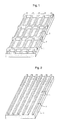
- Fig. 1 is a schematic view showing one embodiment of a substrate for PDP on which a barrier rib is formed.
- Fig. 2 is a schematic view showing one embodiment of a substrate for PDP on which a barrier rib is formed.
- Fig. 3 is a schematic view showing one embodiment of the respective steps of the process for preparing a phosphor pattern according to the present invention.
- Fig. 4 is a schematic view showing the width of the barrier rib of the present invention and the width of an opening at the concave portion.
- Fig. 5 is a schematic view showing an inner surface at the concave portion to be photocured.
- Fig. 6 is a schematic view showing the state after subjecting the step (III) when a photomask 6 having a broader opening width than the opening width of the concave portion in the step (II) of the present invention.
- Fig. 7 is a schematic view showing the state of forming a multi-colored pattern comprising the photosensitive resin composition layer containing a phosphor.
- Fig. 8 is a schematic view showing the state of forming a multi-colored phosphor pattern.
- Fig. 9 is a schematic view showing the state of forming a phosphor pattern without using a sheet having a light scattering function.
- Fig. 10 is a schematic view showing one embodiment of a back plate for a plasma display panel of the present invention.
- a process for preparing a phosphor pattern of the present invention comprises the steps of (I) forming a phosphor-containing photosensitive resin composition layer (A) on a substrate having unevenness, (II) irradiating a scattered light to the phosphor-containing photosensitive resin composition layer (A) imagewisely, (III) developing the phosphor-containing photosensitive resin composition layer (A) by removing the portion to which the scattered light is imagewisely irradiated to form a pattern, and (IV) calcinating the formed pattern to remove an unnecessary portion from the pattern formed in the step (III) to form a phosphor pattern.
- a substrate for a plasma display panel (a substrate for PDP) on which a barrier rib is formed.
- the substrate for PDP there may be mentioned, for example, a substrate such as a glass plate and a synthetic resin plate, which may be subjected to surface treatment for transparent adhesion and on which an electrode and a barrier rib are formed.
- Formation of a barrier rib is not particularly limited, and a known material may be used.
- a rib material containing silica, a binder such as a thermoplastic resin and a thermosetting resin, a low melting point glass (e.g., lead oxide) and a solvent may be used.
- a dielectric film, an insulating film, an auxiliary electrode and a resistor may be formed, if necessary.
- a method for forming the above members on the substrate is not particularly limited.
- an electrode can be formed on the substrate by a method such as vapor deposition, sputtering, plating, coating and printing, and a barrier rib can be formed on the substrate by a method such as a printing method, a sand blasting method and an embedding method.
- Fig. 1 and Fig. 2 each show a schematical view of one embodiment of the substrate for PDP on which a barrier rib is formed.
- the barrier rib generally has a height of 20 to 500 ⁇ m and a width of 20 to 200 ⁇ m.
- the shape of a discharge space surrounded by the barrier rib is not particularly limited and may be lattice-shaped, striped, honeycomb-shaped, triangular or elliptical. In general, a lattice-shaped or striped discharge space as shown in Fig. 1 or Fig. 2 is formed.
- a barrier rib 2 is formed on a substrate 1.
- a lattice-shaped discharge space 3 is formed, and in Fig. 2, a striped discharge space 4 is formed.
- the size of the discharge space is determined by the size and resolution of PDP.
- the longitudinal and lateral lengths are 50 ⁇ m to 1 mm
- the interval is 30 ⁇ m to 1 mm.
- composition of the phosphor-containing photosensitive resin composition layer (A) of the present invention is not particularly limited and can be constituted by using a photosensitive resin composition usually employed in the photolithography method, but in the points of photosensitivity and operatability or workability, it is preferably contain (a) a film property-imparting polymer, (b) a photopolymerizable unsaturated compound having an ethylenically unsaturated group, (c) a photopolymerization initiator which forms free radical by irradiation of the active light, and (d) a phosphor.
- the phosphor-containing photosensitive resin composition layer (A) of the present invention preferably contains, as (b) the photopolymerizable unsaturated compound having an ethylenically unsaturated group, polyethylene glycol di(meth)acryalte, polypropylene glycol di(meth)acrylate, poly(ethylene ⁇ propylene)glycol di(meth)acrylate which have good thermal decomposition property since an unnecessary portion shall be removed by calcination when preparing a phosphor pattern.
- any components other than (d) the phosphor and the binder constituting the photosensitive resin composition preferably do not contain any elements other than carbon, hydrogen, oxygen and nitrogen as a constitutional element.
- the formulation amount of Component (a) in the present invention is preferably 10 to 90 parts by weight, more preferably 20 to 80 parts by weight based on the total amount of Component (a) and Component (b) as 100 parts by weight. If the formulation amount is less than 10 parts by weight, when the resulting material is supplied as a photosensitive element in a roll state, a phosphor-containing photosensitive resin is exuded from a roll edge portion (hereinafter referred to as "edge fusion") so that it is difficult to carry out drawing from a roll at the time of lamination of a photosensitive element, and an exuded portion is partially and excessively embedded in the space of the substrate for PDP, whereby a problem of significant lowering of production yield is caused or film-forming property tends to be lowered. If the formulation amount exceeds 90 parts by weight, sensitivity tends to be insufficient.
- the formulation amount of Component (b) in the present invention is preferably 10 to 90 parts by weight, more preferably 20 to 80 parts by weight based on the total amount of Component (a) and Component (b) as 100 parts by weight. If the formulation amount is less than 10 parts by weight, the sensitivity of a phosphor-containing photosensitive resin composition tends to be insufficient. If the formulation amount exceeds 90 parts by weight, a photocured product tends to be brittle, and when a photosensitive element is prepared, a phosphor-containing photosensitive resin composition tends to be exuded from an edge portion by flowing, or film-forming property tends to be lowered.
- the formulation amount of Component (c) in the present invention is preferably 0.01 to 30 parts by weight, more preferably 0.1 to 20 parts by weight based on the total amount of Component (a) and Component (b) as 100 parts by weight. If the formulation amount is less than 0.01 part by weight, the sensitivity of a phosphor-containing photosensitive resin composition tends to be insufficient. If the formulation amount exceeds 30 parts by weight, photocuring of an inner portion tends to be insufficient due to increase in absorption of active light at an exposed surface of a phosphor-containing photosensitive resin composition.
- the formulation amount of Component (d) in the present invention is preferably 10 to 400 parts by weight, more preferably 50 to 350 parts by weight, particularly preferably 70 to 300 parts by weight based on the total amount of Component (a), Component (b) and Component (c) as 100 parts by weight. If the formulation amount is less than 10 parts by weight, when light is emitted as PDP, light emission efficiency tends to be lowered. If the formulation amount exceeds 400 parts by weight, when a photosensitive element is prepared, film-forming property tends to be lowered, or flexibility tends to be lowered.
- a plasticizer may be added to improve film property.
- examples thereof may include a polyalkylene glycol such as a polypropylene glycol represented by the following formula (I): wherein R 1 represents a hydrogen atom or a methyl group, Y 1 represents a hydrogen atom, a saturated hydrocarbon group which may have a substituent or a polyalkylene glycol residue, Y 2 represents a hydroxyl group, a saturated hydrocarbon group which may have a substituent or a polyalkylene glycol residue, and p represents an integer of 1 to 100, provided that R 1 is a hydrogen atom, at least one of Y 1 and Y 2 represents a polypropylene glycol residue, and a derivative thereof, and a polyethylene glycol and a derivative thereof; and dioctylphthalate, diheptylphthalate, dibutylphthalate, tricresylphosphate, cresyldiphenylphosphate, and biphenyldiphenylphosphate.
- a polyalkylene glycol such as a polypropy
- the plasticizer When the plasticizer is formulated, its formulation amount is preferably 0.01 to 90 parts by weight, more preferably 0.01 to 80 parts by weight, particularly preferably 0.01 to 70 parts by weight based on the total amount of Component (a) and Component (b) as 100 parts by weight. If the formulation amount exceeds 90 parts by weight, the sensitivity of a phosphor-containing photosensitive resin composition tends to be insufficient.
- a compound having a carboxyl group may be added to improve storage stability without causing increase in viscosity for a long period of time.
- the compound having a carboxyl group may include, for example, a saturated aliphatic acid, an unsaturated aliphatic acid, an aliphatic dibasic acid, an aromatic dibasic acid, an aliphatic tribasic acid, an aromatic tribasic acid, and the like.
- the compound having a carboxyl group When the compound having a carboxyl group is formulated, its formulation amount is preferably 0.01 to 30 parts by weight based on the amount of Component (a) as 100 parts by weight. If the formulation amount is less than 0.01 part by weight, the storage stability tends to be low, while if it exceeds 30 parts by weight, the sensitivity of a phosphor-containing photosensitive resin composition tends to be insufficient.
- a dispersant is preferably added to improve dispersibility of the phosphor.
- the dispersant may include inorganic dispersants (silica gel type, bentonite type, kaolinite type, talc type, hectorite type, montmolironite type, saponite type, beidellite type dispersants), organic dispersants (aliphatic amide type, aliphatic ester type, polyethylene oxide type, sulfate type anionic surfactant, polycarboxylic acid amine salt type, polycarboxylic acid type, polyamide type, high molecular weight polyether type, acryl copolymer type, specific silicone type dispersants) and the like.
- inorganic dispersants sica gel type, bentonite type, kaolinite type, talc type, hectorite type, montmolironite type, saponite type, beidellite type dispersants
- organic dispersants aliphatic amide type, aliphatic ester type, polyethylene oxide type, sulfate type anionic surfactant, polycarboxylic acid
- These dispersants may be used alone or in combination of two or more.
- the dispersant When the dispersant is formulated, its formulation amount is preferably 0.01 to 100 parts by weight based on the amount of Component (a) as 100 parts by weight. If the formulation amount is less than 0.01 part by weight, the added effect tend to be not revealed, while if it exceeds 100 parts by weight, the pattern formation precision (a property of obtaining a pattern comprising the photosensitive resin composition layer containing a phosphor with precise dimension and desired shape after development) tends to be lowered.
- a binder is preferably added to prevent peel off of the phosphor from the PDP barrier rib substrate after calcination.
- binder may include, for example, a low-melting point glass, a metal alkoxide, a silane coupling agent and the like. These binders may be used alone or in combination of two or more.
- the binder When the binder is formulated, its formulation amount is not particularly limited and preferably 0.01 to 100 parts by weight, more preferably 0.05 to 50 parts by weight, particularly preferably 0.1 to 30 parts by weight based on the amount of Component (d) as 100 parts by weight. If the formulation amount is less than 0.01 part by weight, the binding effect tend to be not revealed, while if it exceeds 100 parts by weight, emission efficiency tends to be lowered.
- a dye for the photosensitive resin composition constituting the phosphor-containing photosensitive resin composition layer (A) of the present invention, a dye, a color forming agent, a plasticizer, a pigment, a polymerization inhibitor, a surface modifier, a tackifier, a heat curing agent, etc. may be added depending on necessity.
- the method for forming the phosphor-containing photosensitive resin composition layer (A) on a substrate having unevenness is not specifically limited, and, for example, it can be carried out by the method in which respective components constituting the phosphor-containing photosensitive resin composition layer (A) is dissolved in or mixed with a solvent which can dissolve or disperse the components to form a uniform solution or dispersion, then the solution or dispersion is directly coated on the substrate having unevenness and dried to form the layer, or the method in which it is formed on the substrate having unevenness by using a photosensitive element having the phosphor-containing photosensitive resin composition layer (A) or the like.
- the method of forming the pattern by using a photosensitive element having the phosphor-containing photosensitive resin composition layer (A) on the substrate having unevenness is preferred since the method allows to form a phosphor pattern with uniform thickness and flexibility.
- the photosensitive element to be used in the method of forming the pattern by using a photosensitive element having the phosphor-containing photosensitive resin composition layer (A) on the substrate having unevenness can be obtained by dissolving the respective components constituting the phosphor-containing photosensitive resin composition layer (A) or mixing the same with a solvent which can dissolve the components or disperse the same to form a uniform solution or dispersion, then coating the solution or dispersion directly on a substrate film such as polyethylene terephthalate, etc. by the conventionally known method and drying the same.
- the method of forming the pattern by using a photosensitive element having the phosphor-containing photosensitive resin composition layer (A) on the substrate having unevenness there may be mentioned, for example, the method in which the phosphor-containing photosensitive resin composition layer (A) of the photosensitive element is laminated on the substrate having unevenness, embedding the same by heating or pressing to form the phosphor-containing photosensitive resin composition layer (A) on the inner surface of the concave portion, the method in which the phosphor-containing photosensitive resin composition layer (A) is embedded in the concave portion by heating or pressing using an embedding layer to form the phosphor-containing photosensitive resin composition layer (A) on the inner surface of the concave portion, or the like.
- the method of forming a pattern by laminating the phosphor-containing photosensitive resin composition layer (A) of the photosensitive element on the substrate having unevenness, embedding the same by heating or pressing on the inner surface of the concave portion there may be mentioned, for example, when a cover film exist in the photosensitive element, after removing the cover film, the phosphor-containing photosensitive resin composition layer (A) is placed on the substrate having unevenness so as to contact with the same, and contact bonding the same under heating, or the like.
- operations of the above contact bonding and contact bonding under heating may be carried out under a reduced pressure of 5 x 10 4 Pa or less.
- the embedding layer is deformed by giving an energy such as heat, pressure and the like, and the phosphor-containing photosensitive resin composition layer (A) is embedded inside the concave portion of the substrate having unevenness by utilizing deformation of the embedding layer to form the phosphor-containing photosensitive resin composition layer (A) on the inner surface of the concave portion.
- the method there may be mentioned, for example, the method in which the phosphor-containing photosensitive resin composition layer (A) derived from the above-mentioned photosensitive element is provided on the substrate having unevenness, and an embedding layer such as the thermoplastic resin layer (B) is subjected to contact bonding under heating under the state that the embedding layer is provided on the phosphor-containing photosensitive resin composition layer (A), or the like.
- a resin constituting the thermoplastic resin layer (B) is not particularly limited so long as it is softened at temperature at the time of contact bonding under heating, and there may be mentioned, for example, polyethylene, polypropylene, polyvinyl chloride, polyvinyl acetate, polyvinylidene chloride, polystyrene, polyvinyltoluene, polyacrylate, polymethacrylate, a copolymer of ethylene and vinyl acetate, a copolymer of ethylene and acrylate, a copolymer of vinyl chloride and vinyl acetate, a copolymer of styrene and acrylate or methacrylate, a copolymer of vinyltoluene and acrylate or methacrylate, a polyvinyl alcohol type resin (e.g., a hydrolyzate of polyacrylate or polymethacrylate, a hydrolyzate of polyvinyl acetate, a hydrolyzate of a copolymer
- thermoplastic resin layer (B) of the present invention for the purpose of suppressing migration to the thermoplastic resin layer (B), there may be added depending on necessity a photopolymerizable unsaturated compound having an ethylenically unsaturated group, a photoinitiator forming free radicals by irradiation of active light, a compound having a carboxyl group, a dye, a color forming agent, a plasticizer, a polymerization inhibitor, a surface modifier, a stabilizer, a tackifier and a heat curing agent.
- a photopolymerizable unsaturated compound having an ethylenically unsaturated group for the purpose of suppressing migration to the thermoplastic resin layer (B)
- a photoinitiator forming free radicals by irradiation of active light
- a compound having a carboxyl group a dye, a color forming agent
- plasticizer a polymerization inhibitor
- surface modifier e.g., a stabilizer,
- those which are formed to a sheet state by a melt extrusion method may be used as an embedding layer.
- the method of providing the phosphor-containing photosensitive resin composition layer (A) derived from the above-mentioned photosensitive element on the substrate having unevenness, and contact bonding under heating an embedding layer such as the thermoplastic resin layer (B) under the state that the embedding layer is provided on the phosphor-containing photosensitive resin composition layer (A) there may be mentioned, for example, the method in which the above-mentioned photosensitive element is laminated on the substrate having unevenness, after removing a support film when the support film exist on the element, the thermoplastic resin layer (B) (after removing a cover film when the cover film exist on the layer) is provided on the phosphor-containing photosensitive resin composition layer (A), and the laminate is subjected to contact bonding under heating by heating rolls.
- operations of the above contact bonding and contact bonding under heating may be carried out under a reduced pressure of 5 x 10 4 Pa or less.
- the embedding layer such as the thermoplastic resin layer (B) and the photosensitive element having the phosphor-containing photosensitive resin composition layer (A)
- it may be carried out to laminate the phosphor-containing photosensitive resin composition layer (A) and the thermoplastic resin layer (B) (these layer (A) and layer (B) are separately supplied) so that the phosphor-containing photosensitive resin composition layer (A) is in contact with the surface of the substrate having unevenness by subjecting these two layers simultaneously to contact bonding under heating.
- a photosensitive element in which an embedding layer such as the thermoplastic resin layer (B) and the phosphor-containing photosensitive resin composition layer (A) are integrated is laminated on the substrate having unevenness so as to contact the phosphor-containing photosensitive resin composition layer (A) to the substrate, and subjected these two layers simultaneously to contact bonding under heating.
- Fig. 3 is a schematic view showing one example of the respective steps of a process for preparing the phosphor pattern of the present invention.
- Fig. 3 (I) the state of forming the phosphor-containing photosensitive resin composition layer (A) 5 on a substrate 1 (a substrate having unevenness) for a PDP to which a barrier rib 2 is formed.
- step (I) of the present invention when an embedding layer is used, an embedding layer exist on the phosphor-containing photosensitive resin composition layer (A) 5 in Fig. 3 (I).
- step (II) there may be mentioned, for example, (IIa) a step of irradiating active light to the phosphor-containing photosensitive resin composition layer (A) through a photomask provided on the photosensitive resin composition layer and a sheet having a light scattering function provided on the photomask, (IIb) a step of irradiating active light to the phosphor-containing photosensitive resin composition layer (A) through a sheet having a light scattering function provided on the photosensitive resin composition layer and a photomask provided on the sheet, and (IIc) a step of irradiating active light to the phosphor-containing photosensitive resin composition layer (A) through a photomask in which the light transmission portion has a light scattering function provided on the photosensitive resin composition layer.
- IIa a step of irradiating active light to the phosphor-containing photosensitive resin composition layer (A) through a photomask provided on the photosensitive resin composition layer and a sheet having a light scattering function provided
- step (IIa) the step of irradiating active light to the phosphor-containing photosensitive resin composition layer (A) through a photomask provided on the photosensitive resin composition layer and a sheet having a light scattering function provided on the photomask which is one embodiment of the step (II) is explained.
- This step (IIa) is shown in Fig. 3 (II).
- a photomask 6 that in which the width of the light transmission portion is narrower than that of an opening at the concave portion of the substrate can be used.
- An opening portion 9 of the concave portion and the width 10 of the barrier rib of the present invention are shown in Fig. 4.
- Fig. 5 is a schematic view showing an inner surface of the concave portion, and in Fig. 5, the inner surface of the concave portion 11 are shaded.
- the width of the above light transmission portion is preferably from a width in which the widths 10 of the barrier ribs at the both sides of the opening are added to the width 9 of the opening of the concave portion (when the width 10 of the barrier rib is 70 ⁇ m, it is a width of 140 ⁇ m wider than the width 9 of the opening of the concave portion) to a width of 120 ⁇ m narrower than the width 9 of the opening of the concave portion, more preferably a width in which 50 % of the width 10 of the barrier ribs at the both sides of the opening are added to the width 9 of the opening of the concave portion (when the widths 10 of the barrier rib is 70 ⁇ m, it is a width of 70 ⁇ m wider than the width 9 of the opening of the concave portion) to a width of 90 ⁇ m narrower than the width 9 of the opening of the concave portion, particularly preferably a width of 1 ⁇ m to 60 ⁇ m narrower than the width 9 of the opening of the conca
- development resistance (a property that a portion which is to be remained without removing by the development is not eroded by the developing solution) of the phosphor-containing photosensitive resin composition layer (A) 5 formed on the inner surface of the concave portion tends to be lowered, and the necessary portion of the phosphor-containing photosensitive resin composition layer (A) 5 formed on the inner surface of the concave portion tends to be removed.
- active light transmission width of the width 9 of the opening at the concave portion represents active light transmission width at the width 9 of the opening at the concave portion of 150 ⁇ m and the width 10 of the barrier rib of 70 ⁇ m. Accordingly, when the dimension of the width 9 of the opening at the concave portion fluctuates, a narrower range of the active light transmission width than the above width 9 of the opening at the concave portion is determined depending on the fluctuation ratio.
- the sheet 7 having a light scattering function of the present invention can be any material so long as it is possible to refract or scatter light.
- the photosensitive resin composition layer 5 containing a phosphor formed on the inner surface of the concave portion can be selectively photocured with high reactivity at both of the barrier rib wall portion and the substrate bottom portion which are inner surfaces of the concave portion.
- the position of the sheet 7 having a light scattering function at use may be any position so long as it locates between the photomask 6 and the active light source. It may be used with a distance of 0.3 to 30 cm apart from the photomask 6 or may be used in contact with the photomask 6.
- Examples of the sheet 7 having a light scattering function may include Quilting Meiler (trade name, available from ORC Seisakusho) and an exposure film having unevenness on the film surface, embossed film, film mat, sand mat film, bloomed glass, frosted glass, designed glass, a material in which a film or glass which transmits general-purpose active light is ground by a laser beam to make the surface uneven, a material in which glass is treated by hydrogen fluoride, etc. (respective glasses mentioned above mean a sheet or plate glass) to make the surface uneven, and a film containing fine particles to scatter light. These materials may be used alone or in combination of two or more.
- the sheet 7 having a light scattering function may be any materials wherein a material in which the light scattering function is provided only one surface thereof, a material in which the light scattering functions are provided to both surfaces, a material in which different light scattering functions are provided to the surface and the back surface, a material in which light scattering functions are provided to the inside and one surface thereof, a material in which the light scattering functions are provided to the inside and both surfaces, and a material in which different light scattering functions are provided to the inside and the surface and the back surface.
- active light may be irradiated to either of the surfaces.
- the surface roughness of the sheet 7 having a light scattering function in which the surface has been treated preferably has a surface roughness Ra (Arithmetical mean deviation roughness) of 0.1 ⁇ m or more, more preferably 0.15 ⁇ m or more, particularly preferably 0.2 ⁇ m or more. If the surface roughness Ra is less than 0.1 ⁇ m, light scattering does not take place sufficiently so that the phosphor-containing photosensitive resin composition layer (A) at the barrier rib side surface portion tends to be eroded.
- An amount of an alien substance contained in the sheet 7 having a light scattering function and containing alien substances therein is preferably 0.1 to 200 % by volume, more preferably 1 to 150 % by volume, particularly preferably 3 to 100 % by volume based on the volume (100 % by volume) of the sheet 7 having a light scattering function. If the amount of the alien substance contained in the sheet 7 having a light scattering function is less than 0.1 % by volume, light scattering does not sufficiently occur so that the phosphor-containing photosensitive resin composition layer (A) at the barrier rib side surface portion tends to be eroded, while if it exceeds 200 % by volume, the exposure time becomes relatively long and an operation efficiency tends to be lowered.
- a transmittance of the sheet 7 having a light scattering function is preferably 1 to 100 %, more preferably 3 to 100 %, more preferably 10 to 100 %, further preferably 30 to 100 %, most preferably 50 to 100 % as compared with the case where no sheet having a light scattering function is used at the wavelength region of 230 nm to 450 nm.
- the transmittance of the sheet 7 having a light scattering function is less than 1 %, the exposure time becomes relatively long and an operation efficiency tends to be lowered.
- a thickness of the sheet 7 having a light scattering function may be any range so long as its transmittance is 1 to 100 % as compared with the case where no sheet having a light scattering function is used at the wavelength region of 230 nm to 450 nm, but the thickness is usually 5 ⁇ m to 1 cm.
- the photomask to be used in the step (IIa) is not particularly limited and conventionally known materials can be used.
- it may include a negative film, a negative glass, a positive film, and a positive glass, etc.
- Such a photomask is also used in the step (IIb).
- the photomask having a light scattering function at the light transmitting portion to be used in the step (IIc) can be prepared by, for example, the method in which an opening portion of a photomask having no light scattering function at the light transmitting portion is treated by a laser or hydrogen fluoride, the method in which a surface of a photomask having no light scattering function at the light transmitting portion at which no light shielding portion is provided is polished by a sand paper, etc. to form uneven thereon, and the method in which a light shielding portion is provided to a sheet having a light scattering function by the conventionally known method, or the like.
- the surface roughness of the photomask having a light scattering function in which the surface has been treated has preferably a surface roughness Ra (center line average roughness) of 0.1 ⁇ m or more, more preferably 0.15 ⁇ m or more, particularly preferably 0.2 ⁇ m or more. If the surface roughness Ra is less than 0.1 ⁇ m, light scattering does not take place sufficiently so that the phosphor-containing photosensitive resin composition layer (A) at the barrier rib side surface portion tends to be eroded.
- Ra center line average roughness
- An amount of an alien substance contained in the photomask having a light scattering function and containing alien substances therein is preferably 0.1 to 200 % by volume, more preferably 1 to 150 % by volume, particularly preferably 3 to 100 % by volume based on the volume (100 % by volume) of the photomask having a light scattering function. If the amount of the alien substance contained in the photomask having a light scattering function is less than 0.1 % by volume, light scattering does not sufficiently occur so that the phosphor-containing photosensitive resin composition layer (A) at the barrier rib side surface portion tends to be eroded, while if it exceeds 200 % by volume, the exposure time becomes relatively long and an operation efficiency tends to be lowered.
- those having a wider active light transmission width to a narrower active light transmission width than the width of the opening portion of the concave portion can be used.
- active light 8 can be imagewisely irradiated after removing the embedding layer by peeling off or development.
- the embedding layer comprises a material which transmits the active light 8
- the active light 8 can be imagewisely irradiated to the embedding layer through a photomask 6 and a sheet 7 having a light scattering function in the state of existing the embedding layer.
- the active light 8 a known active light source may be used, and there may be mentioned, for example, light generated from carbon arc, mercury vapor arc, xenon arc or light generated from the others and the like.
- the irradiation dose of the active light 8 of the present invention is not particularly limited, and preferably 5 to 20,000 mJ/cm 2 , more preferably 7 to 10,000 mJ/cm 2 , particularly preferably 10 to 5,000 mJ/cm 2 . If the irradiation dose of the active light 8 is less than 5 mJ/cm 2 , photocuring of the phosphor-containing photosensitive resin composition layer (A) 5 formed on the inner surface of the concave portion tends to be insufficient.
- development resistance (a property that a portion which is to be remained without removing by the development is not eroded by the developing solution) of the phosphor-containing photosensitive resin composition layer (A) 5 formed on the inner surface of the concave portion tends to be lowered.
- the irradiation dose of the active light 8 exceeds 20,000 mJ/cm 2
- a portion other than the inner surface of the concave portion to be photocured tends to be photocured so that unnecessary portion tends to be remained after development as mentioned below.
- step (II) fine particles, etc. are spread on the phosphor-containing photosensitive resin composition layer (A), and active light can be imagewisely irradiated with the state that the light scattering effect is heightened.
- Fig. 3 (III) The state in which an unnecessary portion is removed by development is shown in Fig. 3 (III).
- the reference numeral 5' is the phosphor-containing photosensitive resin composition layer (A) after photocuring.
- Fig. 3 (III) as the developing method, for example, after the state of Fig. 3 (II), when a support film exists on the phosphor-containing photosensitive resin composition layer (A), after removing it (when an embedding layer exists on the phosphor-containing photosensitive resin composition layer (A) 5, and a support film exists on the embedding layer, after removing it), development is carried out by the conventional method such as spraying, dipping under rocking, brushing, scraping, etc. by using the conventionally known developing solution such as an aqueous alkaline solution, an aqueous developing solution, an organic solvent, etc. to remove the unnecessary portion.
- the conventional method such as spraying, dipping under rocking, brushing, scraping, etc. by using the conventionally known developing solution such as an aqueous alkaline solution, an aqueous developing solution, an organic solvent, etc.
- a base of the aqueous alkaline solution remained at the phosphor-containing photosensitive resin composition layer (A) 5' after photocuring can be treated by an acid (neutralization treatment) by using an organic acid, an inorganic acid or an aqueous solution of these acids according to the conventional method such as spraying, dipping under rocking, brushing, scraping, etc.
- an organic acid such as a saturated aliphatic acid, an unsaturated aliphatic acid, an aliphatic dibasic acid, an aromatic dibasic acid, an aliphatic tribasic acid, an aromatic tribasic acid.
- the phosphor-containing photosensitive resin composition layer (A) (unnecessary portion) formed on the portion other than the inner surface of the concave portion (when an embedding layer exists on the phosphor-containing photosensitive resin composition layer (A) 5, the embedding layer, or when the embedding layer has photosensitivity, the embedding layer other than the inner surface of the concave portion) is removed by development, and on the inner surface of the concave portion, the phosphor-containing photosensitive resin composition layer (A) 5' after photocuring (when the embedding layer having photosensitivity exists on the phosphor-containing photosensitive resin composition layer (A) 5, the embedding layer after photocuring is included) is formed.
- step (II) when a photomask 6 having a wider opening width than the opening width of the concave portion is used, the irradiated portion (when the embedding layer having photosensitivity exists on the phosphor-containing photosensitive resin composition layer (A) 5, the irradiated portion is included) of the phosphor-containing photosensitive resin composition layer (A) 5 formed at the portion other than the inner surface of the concave portion tends to become the state as shown in Fig. 6 by performing the present step (step (III)).
- the phosphor-containing photosensitive resin composition layer (A) 5' (unnecessary portion) after curing remained at other than the inner surface of the concave portion (when the embedding layer having photosensitivity exists on the phosphor-containing photosensitive resin composition layer (A) 5, the embedding layer after photocuring is included) can be completely removed by polishing, etc.
- Fig. 6 is a schematic view showing the state after conducting the step (III) when a photomask 6 which has a wider opening width than the opening width of the concave portion is used in the step (II) of the present invention.
- the reference numeral 12 is an unnecessary portion (a portion which should be completely removed by polishing, etc.).
- only the unnecessary portion can be physically removed by adhering an adhesive tape to the above-mentioned unnecessary portion and peeling off the tape.
- UV-ray irradiation by a high pressure mercury lamp or heating with a dryer may be carried out.
- step (IV) A step of calcinating the formed pattern to remove an unnecessary portion from the pattern formed in the step (III) to form a phosphor pattern.
- Fig. 3 (IV) the state of forming a phosphor pattern after removing the unnecessary portion by calcination is shown.
- the reference numeral 13 is a phosphor pattern.
- the calcination method is not particularly limited, and the phosphor pattern can be formed by using a conventionally known calcination method to remove the unnecessary portion other than the phosphor and binder.
- the calcination temperature at this time is preferably 350 to 800 °C, more preferably 400 to 600 °C. Also, the calcination time is preferably 3 to 120 minutes, more preferably 5 to 90 minutes.
- the temperature elevating rate at this time is preferably 0.5 to 50 °C/min, more preferably 1 to 45 °C/min. Also, between 350 °C and 450 °C which are before reaching to the maximum calcination temperature, a step of maintaining the temperature may be provided and the maintaining time is preferably 5 to 100 minutes.
- the above-mentioned respective steps (I) to (III) are repeated for each color to form a multi-colored pattern comprising the photosensitive resin composition layers containing phosphors which form colors of red, green and blue, and then the step (IV) is performed to form a multi-colored phosphor pattern.
- the phosphor-containing photosensitive resin composition layer (A) 5 which independently contains respective phosphors which form colors red, blue and green can be formed in any order with regard to the respective colors of red, blue and green.
- Fig. 7 the state in which a multi-colored pattern containing the phosphor-containing photosensitive resin composition layer which forms colors of red, green and blue is formed by repeating the respective steps of (I) to (III) for each color is shown.
- the reference numeral 5'a is a first color pattern
- 5'b is a second color pattern
- 5'c is a third color pattern.
- FIG. 8 the state in which the step (IV) of the present invention is performed to form a multi-colored phosphor pattern is shown.
- the reference numeral 13a is a first phosphor pattern
- 13b is a second phosphor pattern
- 13c is a third phosphor pattern.
- the process for preparing the phosphor pattern of the present invention is preferably carried out by repeating the respective steps (I) to (IV) as mentioned above for each color to form a multi-colored phosphor pattern in view of suppression of decrease in film thickness of the phosphor-containing photosensitive resin composition layer (A) 5 formed on the inner surface of the concave portion.
- the phosphor pattern of the present invention preferably satisfies the relation of the layer thickness ratio x/y within the range of 0.1 to 1.5 in the points of luminance, a light utilization ratio, etc., more preferably within the range of 0.15 to 1.3, particularly preferably within the range of 0.2 to 1.2, when the height of the barrier rib is made L ( ⁇ m), a film thickness x ( ⁇ m) of the phosphor pattern formed at the position of 0.9 x L of the barrier rib wall, and a film thickness y ( ⁇ m) of the same formed at the position of 0.4 x L of the barrier rib wall.
- the layer thickness ratio x/y is preferably within the range of 0.1 to 0.5, more preferably 0.15 to 0.45, particularly preferably 0.2 to 0.4 in the point that a utilization ratio of visible light emitted from the phosphor can be increased.
- the layer thickness ratio x/y is preferably within the range of 0.5 to 1.5, more preferably 0.55 to 1.3, particularly preferably 0.6 to 1.2 in the point that lowering in the apparent luminance by seeing from a wide-view angle can be suppressed.
- the back plate for a plasma display panel of the present invention comprises providing phosphor pattern obtained as mentioned above on the substrate for a plasma display panel.
- Fig. 10 is a schematic view showing one example of a plasma display panel (PDP), and in Fig. 10, the reference numeral 1 is a substrate, 2 is a barrier rib, 4 is a stripe shaped discharging space, 13 is a phosphor pattern, 14 is an electrode for address, 16 is a protective film, 17 is a dielectric layer, 18 is an electrode for display, and 19 is a substrate for a front plate.
- PDP plasma display panel
- the reference numeral 1 is a substrate
- 2 is a barrier rib
- 4 is a stripe shaped discharging space
- 13 is a phosphor pattern
- 14 is an electrode for address
- 16 is a protective film
- 17 is a dielectric layer
- 18 is an electrode for display
- 19 is a substrate for a front plate.
- the bottom portion containing the substrate 1, the barrier rib 2, the phosphor pattern 13 and the electrode for address 18 is a back plate for PDP
- the upper portion including the protective layer 16, the dielectric layer 17, the electrode for display 18 and the substrate for a front plate 19 is a front plate for PDP.
- PDP can be classified into an AC (alternative current) type PDP and a DC (direct current) type PDP, and the schematic view shown in Fig. 10 as one example is the AC type PDP.
- the process for preparing the phosphor pattern of the present invention can be also applied to self-emitting type display such as a field emission display (FED), an electroluminescence display (ELD), etc.
- FED field emission display
- ELD electroluminescence display
- a polymer solution (a - 1) having film-forming property (solid component: 45.5 % by weight) with a weight average molecular weight of 80,000 and an acid value of 130 mg KHO/g.
- Materials Formulation amount Solution (a - 1) having film-forming property obtained in Preparation example 1 132 parts by weight (solid component: 60 parts by weight) 4G (trade name, available from Shin-nakamura Kagaku Kogyo, Polyethylene-glycol dimethacrylate (average number of ethylene oxide: 4)) 40 parts by weight 2-Benzyl-2-dimethylamino-1-(4-morpholinophenyl)-butanone-1 3 parts by weight (Y,Gd)BO 3 :Eu 3+ 140 parts by weight Binder (low melting point glass) 3 parts by weight Methyl ethyl ketone 30 parts by weight
- the resulting solution was uniformly coated on a polyethylene terephthalate film with a thickness of 20 ⁇ m, and dried by a hot-air convection drier at 80 to 110 °C for 10 minutes to remove the solvent and to form a phosphor-containing photosensitive resin composition layer (A).
- the thickness of the resulting phosphor-containing photosensitive resin composition layer (A) after drying was 60 ⁇ m.
- Photosensitive element (A - 1) having the phosphor-containing photosensitive resin composition layer (A).
- a phosphor-containing photosensitive resin composition layer (A) was prepared.
- the film thickness of the resulting phosphor-containing photosensitive resin composition layer (A) after drying was 60 ⁇ m.
- Materials Formulation amount Solution (a - 1) having film-forming property obtained in Preparation example 1 132 parts by weight (solid component: 60 parts by weight) Propyleneglycol dimethacrylate (average number of propylene oxide: 12) 40 parts by weight 2-Benzyl-2-dimethylamino-1-(4-morpholinophenyl)-butanone-1 1 parts by weight (Y,Gd)BO 3 :Eu 3+ 140 parts by weight Methyl ethyl ketone 30 parts by weight
- Photosensitive element (A - 2) having the phosphor-containing photosensitive resin composition layer (A) was prepared.
- a phosphor-containing photosensitive resin composition layer (A) was prepared.
- the film thickness of the resulting phosphor-containing photosensitive resin composition layer (A) after drying was 60 ⁇ m.
- Photosensitive element (A - 3) having the phosphor-containing photosensitive resin composition layer (A) was prepared.
- thermoplastic resin layer (B) A resin solution comprising the materials shown in Table 5 was uniformly coated on a polyethylene terephthalate film having a thickness of 20 ⁇ m, and dried by a hot-air convection drier at 80 to 110 °C for 10 minutes to remove distilled water and to form a thermoplastic resin layer (B). The thickness of the resulting thermoplastic resin layer (B) after drying was 70 ⁇ m.
- thermoplastic resin layer (B) was laminated a polyethylene film having a thickness of 25 ⁇ m as a cover film to prepare Film (B - 1) having the thermoplastic resin layer (B).
- thermoplastic resin layer (B) was prepared.
- the film thickness of the resulting thermoplastic resin layer (B) after drying was 43 ⁇ m.
- Materials Formulation amount Solution (a - 1) having film-forming property obtained in Preparation example 1 143 parts by weight (solid component: 65 parts by weight)
- Triethylene glycol diacetate 35 parts by weight Methyl ethyl ketone 30 parts by weight
- thermoplastic resin layer (B) was prepared.
- the film thickness of the resulting thermoplastic resin layer (B) after drying was 50 ⁇ m.
- Materials Formulation amount Poly(methyl methacrylate) (weight average molecular weight: about 70,000) 70 parts by weight
- Photosensitive element (A - 1) having the phosphor-containing photosensitive resin composition layer (A) obtained in Preparation example 2 was placed while peeling off the polyethylene film, then, the polyethylene terephthalate film was peeled off and the material was placed in a vacuum drier under a vacuum degree of 1.3 x 10 2 Pa at a normal temperature.
- temperature of the material was raised to 90 °C with a rate of 5 °C/min and maintained at 90 °C for 1 minute, and returned to an atmospheric pressure to give a pressure to form the phosphor-containing photosensitive resin composition layer (A) on the inner surface of the concave portion.
- a photomask having an active light transmission width which is 15 ⁇ m narrower than the opening width of 150 ⁇ m between the barrier ribs was closely contacted onto the phosphor-containing photosensitive resin composition layer (A) so as to place the center of the active light transmission width of the photomask at the center of the opening width between barrier ribs and a sheet having a light scattering function (available from ORC Seisakusho, Quilting Meiler, trade name (which is produced by NIPPON CHEM-TECH CORP.
- the material was allowed to stand at normal temperature for one hour, and then, subjected to spray development by using 1 % by weight aqueous sodium carbonate solution at 30 °C for 120 seconds.
- the material was dried at 80 °C for 10 minutes and UV-ray irradiation with 3 J/cm 2 was carried out by using a Toshiba UV-ray irradiating machine (trade name, available from Toshiba Denzai), and further dried at 150 °C for one hour in a drying device.
- a Toshiba UV-ray irradiating machine (trade name, available from Toshiba Denzai)
- heat treatment (calcination) was carried out at 550 °C for 30 minutes to remove an unnecessary resin component whereby a phosphor pattern was formed on the inner surface of the concave portion of the substrate for PDP.
- Photosensitive element (A - 1) including the phosphor-containing photosensitive resin composition layer (A) obtained in Preparation example 2 was laminated by using a vacuum laminator (trade name: VLM-1 Model, produced by Hitachi Chemical Co., Ltd.) at a heat shoe temperature of 30 °C and a lamination rate of 0.5 m/min under an atmospheric pressure of 4,000 Pa or less and a contact bonding pressure (cylinder pressure) of 5 x 10 4 Pa (since a substrate having a thickness of 3 mm, a length of 10 cm and a width of 10 cm was used, line pressure at this time was 2.4 x 10 3 N/m) while the polyethylene film of Photosensitive element (A - 1) was peeled off.
- a vacuum laminator trade name: VLM-1 Model, produced by Hitachi Chemical Co., Ltd.
- the polyethylene terephthalate film of Photosensitive element (A - 1) having the phosphor-containing photosensitive resin composition layer (A) was peeled off.
- Film (B - 1) having the thermoplastic resin layer (B) obtained in Preparation example 3 was laminated, while peeling off the polyethylene film, by using a laminator (trade name: HLM-3000 Model, produced by Hitachi Chemical Co., Ltd.) at a lamination temperature of 110 °C and a lamination rate of 0.5 m/min under a contact bonding pressure (guage pressure (cylinder pressure, normal pressure of 1 atm being 0)) of 4 x 10 5 Pa (since a substrate having a thickness of 3 mm, a length of 10 cm and a width of 10 cm was used, line pressure at this time was 9.8 x 10 3 N/m).
- a laminator trade name: HLM-3000 Model, produced by Hitachi Chemical Co., Ltd.
- the material was allowed to stand at normal temperature for one hour, and then, the polyethylene terephthalate film of Film (B-1) having the thermoplastic resin layer (B) was peeled off, and the resulting material was subjected to spray development by using 1 % by weight aqueous sodium carbonate solution at 30 °C for 120 seconds.
- the material was dried at 80 °C for 10 minutes and UV-ray irradiation with 3 J/cm 2 was carried out by using a Toshiba UV-ray irradiating machine (trade name, available from Toshiba Denzai), and further dried at 150 °C for one hour in a drying device.
- a Toshiba UV-ray irradiating machine (trade name, available from Toshiba Denzai)
- heat treatment (calcination) was carried out at 550 °C for 30 minutes to remove an unnecessary resin component whereby a phosphor pattern was formed on the inner surface of the concave portion of the substrate for PDP.
- the material was dried at 80 °C for 10 minutes and UV-ray irradiation with 3 J/cm 2 was carried out by using a Toshiba UV-ray irradiating machine (trade name, available from Toshiba Denzai), and further dried at 150 °C for one hour in a drying device.
- a Toshiba UV-ray irradiating machine (trade name, available from Toshiba Denzai)
- Example 8 In the same manner as in Example 1 except for changing the step (IIa) to the step (IIb) shown below, a phosphor pattern was formed. A sectional view of the resulting phosphor pattern was observed in the same manner as in Example 1 and the formed state of the phosphor pattern was evaluated. The results are shown in Table 8 mentioned below.
- Example 2 In the same manner as in Example 2 except for changing the step (IIa) to the step (IIb) shown below, a phosphor pattern was formed. A sectional view of the resulting phosphor pattern was observed in the same manner as in Example 1 and the formed state of the phosphor pattern was evaluated. The results are shown in Table 8 mentioned below.
- Example 3 In the same manner as in Example 3 except for changing the step (IIa) to the step (IIb) shown below, a phosphor pattern was formed. A sectional view of the resulting phosphor pattern was observed in the same manner as in Example 1 and the formed state of the phosphor pattern was evaluated. The results are shown in Table 8 mentioned below.
- Example 4 In the same manner as in Example 4 except for changing the step (IIa) to the step (IIb) shown below, a phosphor pattern was formed. A sectional view of the resulting phosphor pattern was observed in the same manner as in Example 1 and the formed state of the phosphor pattern was evaluated. The results are shown in Table 8 mentioned below.
- Example 8 In the same manner as in Example 1 except for changing the step (IIa) to the step (IIc) shown below, a phosphor pattern was formed. A sectional view of the resulting phosphor pattern was observed in the same manner as in Example 1 and the formed state of the phosphor pattern was evaluated. The results are shown in Table 8 mentioned below.
- Example 2 In the same manner as in Example 2 except for changing the step (IIa) to the step (IIc) shown below, a phosphor pattern was formed. A sectional view of the resulting phosphor pattern was observed in the same manner as in Example 1 and the formed state of the phosphor pattern was evaluated. The results are shown in Table 8 mentioned below.
- Example 8 In the same manner as in Example 3 except for changing the step (IIa) to the step (IIc) shown below, a phosphor pattern was formed. A sectional view of the resulting phosphor pattern was observed in the same manner as in Example 1 and the formed state of the phosphor pattern was evaluated. The results are shown in Table 8 mentioned below.
- Example 4 In the same manner as in Example 4 except for changing the step (IIa) to the step (IIc) shown below, a phosphor pattern was formed. A sectional view of the resulting phosphor pattern was observed in the same manner as in Example 1 and the formed state of the phosphor pattern was evaluated. The results are shown in Table 8 mentioned below.
- Example 8 In the same manner as in Example 1 except for changing the step (II) to the step (IIp) as shown below. A sectional view of the resulting phosphor pattern was observed in the same manner as in Example 1 and the formed state of the phosphor pattern was evaluated. The results are shown in Table 8 mentioned below.
- a photomask having an active light transmission width which is 15 ⁇ m narrower than the opening width of 150 ⁇ m between the barrier ribs was closely contaced so as to place the center of the active light transmission width of the photomask at the center of the opening width between barrier ribs, and the material was irradiated imagewisely by active light of 400 mJ/cm 2 using HMW-201GX type exposure machine (trade name, available from ORC Seisakusho).
- Example 2 In the same manner as in Example 2 except for changing the step (II) to the step (IIq) as shown below. A sectional view of the resulting phosphor pattern was observed in the same manner as in Example 1 and the formed state of the phosphor pattern was evaluated. The results are shown in Table 8 mentioned below.
- a photomask having an active light transmission width which is 15 ⁇ m narrower than the opening width of 150 ⁇ m between the barrier ribs was closely contaced so as to place the center of the active light transmission width of the photomask at the center of the opening width between barrier ribs, and the material was irradiated imagewisely by active light of 600 mJ/cm 2 using HMW-201GX type exposure machine (trade name, available from ORC Seisakusho).
- Example 3 In the same manner as in Example 3 except for changing the step (II) to the step (IIr) as shown below. A sectional view of the resulting phosphor pattern was observed in the same manner as in Example 1 and the formed state of the phosphor pattern was evaluated. The results are shown in Table 8 mentioned below.
- a photomask having an active light transmission width which is 35 ⁇ m narrower than the opening width of 150 ⁇ m between the barrier ribs was closely contaced so as to place the center of the active light transmission width of the photomask at the center of the opening width between barrier ribs, and the material was irradiated imagewisely by active light of 400 mJ/cm 2 using HMW-201GX type exposure machine (trade name, available from ORC Seisakusho).
- Example 4 In the same manner as in Example 4 except for changing the step (II) to the step (IIs) as shown below. A sectional view of the resulting phosphor pattern was observed in the same manner as in Example 1 and the formed state of the phosphor pattern was evaluated. The results are shown in Table 8 mentioned below.
- a photomask having an active light transmission width which is 25 ⁇ m narrower than the opening width of 150 ⁇ m between the barrier ribs was closely contaced so as to place the center of the active light transmission width of the photomask at the center of the opening width between barrier ribs, and the material was irradiated imagewisely by active light of 400 mJ/cm 2 using HMW-201GX type exposure machine (trade name, available from ORC Seisakusho).
- Examples 1 to 15 in which a scattered light is imagewisely irradiated are excellent in formability (which is a property in which a phosphor pattern can be formed in uniform thickness only on the inner surface of concave portion surrounded by the wall surface of the barrier ribs and substrate surface for PDP) of a phosphor pattern on the inner surface of the concave portion of the substrate for PDP.
- the photosensitive resin layer containing a phosphor at the wall portions of the barrier ribs are erroded as shown in Fig. 9 so that it can be understood that formability of the phosphor pattern on the inner surface of the concave portion of the substrate for PDP is not so good since the phosphor pattern cannot be formed with a uniform film thickness on the inner surface of the concave portion surrounded by the wall surface of the barrier ribs and substrate surface.
- the reference numeral 14 in Fig. 9 is a phorphor pattern in which the wall surfaces of the barrier ribs are erroded.
Applications Claiming Priority (3)
| Application Number | Priority Date | Filing Date | Title |
|---|---|---|---|
| JP5674897 | 1997-03-11 | ||
| JP5674897 | 1997-03-11 | ||
| JP56748/97 | 1997-03-11 |
Publications (3)
| Publication Number | Publication Date |
|---|---|
| EP0865067A2 true EP0865067A2 (en) | 1998-09-16 |
| EP0865067A3 EP0865067A3 (en) | 1999-04-07 |
| EP0865067B1 EP0865067B1 (en) | 2002-11-27 |
Family
ID=13036155
Family Applications (1)
| Application Number | Title | Priority Date | Filing Date |
|---|---|---|---|
| EP98400575A Expired - Lifetime EP0865067B1 (en) | 1997-03-11 | 1998-03-11 | Processes for preparing phosphor pattern |
Country Status (3)
| Country | Link |
|---|---|
| US (1) | US6194826B1 (es) |
| EP (1) | EP0865067B1 (es) |
| KR (1) | KR19980080127A (es) |
Cited By (2)
| Publication number | Priority date | Publication date | Assignee | Title |
|---|---|---|---|---|
| EP0872870A2 (en) * | 1997-04-14 | 1998-10-21 | Hitachi Chemical Co., Ltd. | Fluorescent pattern, process for preparing the same, organic alkali developing solution for forming the same, emulsion developing solution for forming the same and back plate for plasma display using the same |
| EP0887833A2 (en) * | 1997-05-22 | 1998-12-30 | Hitachi Chemical Co., Ltd. | Process for preparing phosphor pattern for field emission panel, photosensitive element for field emission display panel, phosphor pattern for field emission display panel and field emission display panel |
Families Citing this family (9)
| Publication number | Priority date | Publication date | Assignee | Title |
|---|---|---|---|---|
| KR19990062901A (ko) * | 1997-12-09 | 1999-07-26 | 와까바야시 구니히꾀 | 형광체 페턴의 제조방법, 형광체 페턴형성용 감광성 엘레멘트,형광체 페턴 및 플라스마 디스플레이 페널용 배면판 |
| US6232705B1 (en) | 1998-09-01 | 2001-05-15 | Micron Technology, Inc. | Field emitter arrays with gate insulator and cathode formed from single layer of polysilicon |
| JP3230511B2 (ja) * | 1999-02-04 | 2001-11-19 | 日本電気株式会社 | プラズマディスプレイ装置 |
| US6417016B1 (en) * | 1999-02-26 | 2002-07-09 | Micron Technology, Inc. | Structure and method for field emitter tips |
| US6692323B1 (en) * | 2000-01-14 | 2004-02-17 | Micron Technology, Inc. | Structure and method to enhance field emission in field emitter device |
| KR100393190B1 (ko) * | 2001-03-06 | 2003-07-31 | 삼성전자주식회사 | 평판형광램프 제조방법 |
| KR20040008817A (ko) * | 2002-07-19 | 2004-01-31 | 한경덕 | 컬러브라운관의 형광체 표면 코팅용 코팅액 조성물 |
| KR100739056B1 (ko) * | 2005-11-23 | 2007-07-12 | 삼성에스디아이 주식회사 | 플라즈마 디스플레이 패널 및 그 제조 방법 |
| US8952406B2 (en) | 2012-07-12 | 2015-02-10 | Micron Technology, Inc. | Lighting devices including patterned optical components and associated devices, systems, and methods |
Citations (8)
| Publication number | Priority date | Publication date | Assignee | Title |
|---|---|---|---|---|
| EP0768573A1 (en) * | 1995-10-13 | 1997-04-16 | Hitachi Chemical Co., Ltd. | Phosphor-containing photosensitive resin composition for use in manufacturing plasma display panel |
| EP0785565A1 (en) * | 1996-01-22 | 1997-07-23 | Hitachi Chemical Co., Ltd. | Phosphor pattern, processes for preparing the same and photosensitive element to be used for the same |
| JPH09265184A (ja) * | 1996-03-29 | 1997-10-07 | Hitachi Chem Co Ltd | 感光性エレメント及びこれを用いた蛍光体パターンの製造法 |
| JPH1092313A (ja) * | 1996-02-28 | 1998-04-10 | Hitachi Chem Co Ltd | 蛍光体パターンの製造法、これに用いられる感光性エレメント、蛍光体パターン及びプラズマディスプレイパネル用背面板 |
| JPH10186645A (ja) * | 1996-12-27 | 1998-07-14 | Hitachi Chem Co Ltd | 蛍光体パターンの製造法 |
| JPH10186643A (ja) * | 1996-12-27 | 1998-07-14 | Hitachi Chem Co Ltd | 蛍光体パターンの製造法 |
| JPH10186644A (ja) * | 1996-12-27 | 1998-07-14 | Hitachi Chem Co Ltd | 蛍光体パターンの製造法 |
| JPH10198026A (ja) * | 1997-01-14 | 1998-07-31 | Hitachi Chem Co Ltd | 感光性樹脂組成物、これを用いた感光性エレメント及びこれらを用いた蛍光体パターンの製造法 |
Family Cites Families (1)
| Publication number | Priority date | Publication date | Assignee | Title |
|---|---|---|---|---|
| DE69635600T2 (de) * | 1995-03-09 | 2006-09-14 | Sankei Giken Kogyo K.K. | Harzzusammensetzung für stromlose Metallabscheidung und Verfahren zur stromlosen Metallabscheidung |
-
1998
- 1998-03-11 EP EP98400575A patent/EP0865067B1/en not_active Expired - Lifetime
- 1998-03-11 US US09/038,286 patent/US6194826B1/en not_active Expired - Fee Related
- 1998-03-11 KR KR1019980008089A patent/KR19980080127A/ko not_active Application Discontinuation
Patent Citations (8)
| Publication number | Priority date | Publication date | Assignee | Title |
|---|---|---|---|---|
| EP0768573A1 (en) * | 1995-10-13 | 1997-04-16 | Hitachi Chemical Co., Ltd. | Phosphor-containing photosensitive resin composition for use in manufacturing plasma display panel |
| EP0785565A1 (en) * | 1996-01-22 | 1997-07-23 | Hitachi Chemical Co., Ltd. | Phosphor pattern, processes for preparing the same and photosensitive element to be used for the same |
| JPH1092313A (ja) * | 1996-02-28 | 1998-04-10 | Hitachi Chem Co Ltd | 蛍光体パターンの製造法、これに用いられる感光性エレメント、蛍光体パターン及びプラズマディスプレイパネル用背面板 |
| JPH09265184A (ja) * | 1996-03-29 | 1997-10-07 | Hitachi Chem Co Ltd | 感光性エレメント及びこれを用いた蛍光体パターンの製造法 |
| JPH10186645A (ja) * | 1996-12-27 | 1998-07-14 | Hitachi Chem Co Ltd | 蛍光体パターンの製造法 |
| JPH10186643A (ja) * | 1996-12-27 | 1998-07-14 | Hitachi Chem Co Ltd | 蛍光体パターンの製造法 |
| JPH10186644A (ja) * | 1996-12-27 | 1998-07-14 | Hitachi Chem Co Ltd | 蛍光体パターンの製造法 |
| JPH10198026A (ja) * | 1997-01-14 | 1998-07-31 | Hitachi Chem Co Ltd | 感光性樹脂組成物、これを用いた感光性エレメント及びこれらを用いた蛍光体パターンの製造法 |
Non-Patent Citations (6)
| Title |
|---|
| PATENT ABSTRACTS OF JAPAN vol. 098, no. 002, 30 January 1998 & JP 09 265184 A (HITACHI CHEM CO LTD), 7 October 1997 * |
| PATENT ABSTRACTS OF JAPAN vol. 098, no. 009, 31 July 1998 & JP 10 092313 A (HITACHI CHEM CO LTD), 10 April 1998 * |
| PATENT ABSTRACTS OF JAPAN vol. 098, no. 012, 31 October 1998 & JP 10 186643 A (HITACHI CHEM CO LTD), 14 July 1998 * |
| PATENT ABSTRACTS OF JAPAN vol. 098, no. 012, 31 October 1998 & JP 10 186644 A (HITACHI CHEM CO LTD), 14 July 1998 * |
| PATENT ABSTRACTS OF JAPAN vol. 098, no. 012, 31 October 1998 & JP 10 186645 A (HITACHI CHEM CO LTD), 14 July 1998 * |
| PATENT ABSTRACTS OF JAPAN vol. 098, no. 012, 31 October 1998 & JP 10 198026 A (HITACHI CHEM CO LTD), 31 July 1998 * |
Cited By (7)
| Publication number | Priority date | Publication date | Assignee | Title |
|---|---|---|---|---|
| EP0872870A2 (en) * | 1997-04-14 | 1998-10-21 | Hitachi Chemical Co., Ltd. | Fluorescent pattern, process for preparing the same, organic alkali developing solution for forming the same, emulsion developing solution for forming the same and back plate for plasma display using the same |
| EP0872870A3 (en) * | 1997-04-14 | 1999-05-06 | Hitachi Chemical Co., Ltd. | Fluorescent pattern, process for preparing the same, organic alkali developing solution for forming the same, emulsion developing solution for forming the same and back plate for plasma display using the same |
| US6232024B1 (en) | 1997-04-14 | 2001-05-15 | Hitachi Chemical Co., Ltd. | Fluorescent pattern, process for preparing the same, organic alkali developing solution for forming the same, emulsion developing solution for forming the same and back plate for plasma display using the same |
| US6358663B2 (en) | 1997-04-14 | 2002-03-19 | Hitachi Chemical Co., Ltd. | Fluorescent pattern, process for preparing the same, organic alkali developing solution for forming the same, emulsion developing solution for forming the same and back plate for plasma display using the same |
| EP0887833A2 (en) * | 1997-05-22 | 1998-12-30 | Hitachi Chemical Co., Ltd. | Process for preparing phosphor pattern for field emission panel, photosensitive element for field emission display panel, phosphor pattern for field emission display panel and field emission display panel |
| EP0887833A3 (en) * | 1997-05-22 | 2000-02-02 | Hitachi Chemical Co., Ltd. | Process for preparing phosphor pattern for field emission panel, photosensitive element for field emission display panel, phosphor pattern for field emission display panel and field emission display panel |
| US6391504B2 (en) | 1997-05-22 | 2002-05-21 | Hitachi Chemical Co., Ltd. | Process for preparing phosphor pattern for field emission display panel, photosensitive element for field emission display panel, phosphor pattern for field emission display panel and field display panel |
Also Published As
| Publication number | Publication date |
|---|---|
| KR19980080127A (ko) | 1998-11-25 |
| EP0865067A3 (en) | 1999-04-07 |
| EP0865067B1 (en) | 2002-11-27 |
| US6194826B1 (en) | 2001-02-27 |
Similar Documents
| Publication | Publication Date | Title |
|---|---|---|
| EP0887833B1 (en) | Process for preparing phosphor pattern for field emission panel and photosensitive element | |
| EP0865067B1 (en) | Processes for preparing phosphor pattern | |
| KR100228966B1 (ko) | 형광체 패턴 및 형광체 패턴의 제조법 및 여기에 사용하는 감광 성 엘리먼트 | |
| JPH1062980A (ja) | 感光性樹脂組成物、感光性エレメント及びこれを用いた蛍光体パターンの製造法 | |
| JP2001027802A (ja) | 感光性ペースト、ディスプレイおよびプラズマディスプレイ用部材 | |
| JPH09288974A (ja) | 蛍光体パターンの製造法、蛍光体パターン及びプラズマディスプレイパネル用背面板 | |
| JP3925749B2 (ja) | 積層方法、積層装置、蛍光体パターンの製造法、蛍光体パターン及びプラズマディスプレイパネル用背面板 | |
| JPH11242327A (ja) | 感光性エレメント、その製造方法、感光性エレメントを用いる蛍光体パターンの製造法、蛍光体パターン及びプラズマディスプレイパネル用背面板 | |
| JPH09265184A (ja) | 感光性エレメント及びこれを用いた蛍光体パターンの製造法 | |
| JPH10198026A (ja) | 感光性樹脂組成物、これを用いた感光性エレメント及びこれらを用いた蛍光体パターンの製造法 | |
| JPH11271980A (ja) | 蛍光体パターンの製造法、蛍光体パターン形成用感光性エレメント、蛍光体パターン及びプラズマディスプレイパネル用背面板 | |
| JPH10312749A (ja) | 蛍光体パターンの製造法、蛍光体パターン及びプラズマディスプレイパネル用背面板 | |
| JPH1195420A (ja) | プラズマディスプレイパネル用背面板の製造法 | |
| KR19990062901A (ko) | 형광체 페턴의 제조방법, 형광체 페턴형성용 감광성 엘레멘트,형광체 페턴 및 플라스마 디스플레이 페널용 배면판 | |
| JPH10186644A (ja) | 蛍光体パターンの製造法 | |
| JPH10186643A (ja) | 蛍光体パターンの製造法 | |
| JPH10228103A (ja) | 感光性樹脂組成物、これを用いた感光性エレメント、蛍光体パターンの製造法、これを用いた蛍光体パターン及びプラズマディスプレイパネル用背面板 | |
| JPH09265906A (ja) | 蛍光体パターンの製造法、蛍光体パターン及びプラズマディスプレイパネル用背面板 | |
| JPH09199027A (ja) | 蛍光体パターンの製造法 | |
| JPH11191366A (ja) | 感光性エレメント及びその製造方法、蛍光体パターンの製造法、蛍光体パターン並びにプラズマディスプレイパネル用背面板 | |
| JPH11165366A (ja) | 蛍光体パターンの製造法 | |
| JP2000315455A (ja) | 蛍光体パターンの製造法 | |
| JPH11194484A (ja) | 感光性エレメント及びその製造方法並びに蛍光体パターンの製造法、蛍光体パターン及びプラズマディスプレイパネル用背面板 | |
| JPH1092313A (ja) | 蛍光体パターンの製造法、これに用いられる感光性エレメント、蛍光体パターン及びプラズマディスプレイパネル用背面板 | |
| JPH09199030A (ja) | 感光性エレメント及びこれを用いた蛍光体パターンの製造法 |
Legal Events
| Date | Code | Title | Description |
|---|---|---|---|
| PUAI | Public reference made under article 153(3) epc to a published international application that has entered the european phase |
Free format text: ORIGINAL CODE: 0009012 |
|
| AK | Designated contracting states |
Kind code of ref document: A2 Designated state(s): FR NL |
|
| AX | Request for extension of the european patent |
Free format text: AL;LT;LV;MK;RO;SI |
|
| PUAL | Search report despatched |
Free format text: ORIGINAL CODE: 0009013 |
|
| AK | Designated contracting states |
Kind code of ref document: A3 Designated state(s): AT BE CH DE DK ES FI FR GB GR IE IT LI LU MC NL PT SE |
|
| AX | Request for extension of the european patent |
Free format text: AL;LT;LV;MK;RO;SI |
|
| 17P | Request for examination filed |
Effective date: 19990604 |
|
| AKX | Designation fees paid |
Free format text: FR NL |
|
| REG | Reference to a national code |
Ref country code: DE Ref legal event code: 8566 |
|
| 17Q | First examination report despatched |
Effective date: 20010326 |
|
| GRAG | Despatch of communication of intention to grant |
Free format text: ORIGINAL CODE: EPIDOS AGRA |
|
| RIC1 | Information provided on ipc code assigned before grant |
Free format text: 7H 01J 9/227 A, 7G 03F 7/00 B |
|
| RTI1 | Title (correction) |
Free format text: PROCESSES FOR PREPARING PHOSPHOR PATTERN |
|
| GRAG | Despatch of communication of intention to grant |
Free format text: ORIGINAL CODE: EPIDOS AGRA |
|
| GRAH | Despatch of communication of intention to grant a patent |
Free format text: ORIGINAL CODE: EPIDOS IGRA |
|
| GRAH | Despatch of communication of intention to grant a patent |
Free format text: ORIGINAL CODE: EPIDOS IGRA |
|
| GRAA | (expected) grant |
Free format text: ORIGINAL CODE: 0009210 |
|
| AK | Designated contracting states |
Kind code of ref document: B1 Designated state(s): FR NL |
|
| PGFP | Annual fee paid to national office [announced via postgrant information from national office to epo] |
Ref country code: FR Payment date: 20030226 Year of fee payment: 6 |
|
| PGFP | Annual fee paid to national office [announced via postgrant information from national office to epo] |
Ref country code: NL Payment date: 20030328 Year of fee payment: 6 |
|
| ET | Fr: translation filed | ||
| PLBE | No opposition filed within time limit |
Free format text: ORIGINAL CODE: 0009261 |
|
| STAA | Information on the status of an ep patent application or granted ep patent |
Free format text: STATUS: NO OPPOSITION FILED WITHIN TIME LIMIT |
|
| 26N | No opposition filed |
Effective date: 20030828 |
|
| PG25 | Lapsed in a contracting state [announced via postgrant information from national office to epo] |
Ref country code: NL Free format text: LAPSE BECAUSE OF NON-PAYMENT OF DUE FEES Effective date: 20041001 |
|
| PG25 | Lapsed in a contracting state [announced via postgrant information from national office to epo] |
Ref country code: FR Free format text: LAPSE BECAUSE OF NON-PAYMENT OF DUE FEES Effective date: 20041130 |
|
| NLV4 | Nl: lapsed or anulled due to non-payment of the annual fee |
Effective date: 20041001 |
|
| REG | Reference to a national code |
Ref country code: FR Ref legal event code: ST |