BACKGROUND OF THE INVENTION
Field of the Invention:
The present invention relates to a D-type flip-flop circuit.
Description of Related Art:
Presently, while a frequency dividing circuit operable for higher
frequency is desired in the technology of a PLL frequency synthesizer, a
master-slave type D-type flip-flop circuit composed of bipolar transistors
(hereinafter referred to simply as a transistor) is being used.
FIG. 16 shows a structure of such a D-type flip-flop circuit wherein a
master circuit 161 comprises a differential circuit 162 for inputting data, a
differential circuit 163 for holding data, a current supplying circuit 164 for
supplying a current to the differential circuits 162 and 163 and a switching
circuit 165 for alternately supplying the current to the differential circuits 162
and 163.
The differential circuit 162 comprises transistors q1 and q2 whose
emitters are connected in common, whose bases receive data which are signals
inverted from each other and whose collectors are set as outputs. It is noted
that the collectors of these transistors q1 and q2 are connected to a source
terminal VCC via resistors r1 and r2. While the differential circuit 162 receives
input data which are signals inverted from each other via input terminals d1
and d2, also it may be available one in which one of the input terminals d1 and
d2 is fixed to a reference potential. The differential circuit 163 comprises
transistors q3 and q4 whose emitters are connected in common and whose bases
and collectors are connected across each other. It is noted that the collectors of
the transistors q3 and q4 of the differential circuit 163 are connected to the
collectors of the transistors q1 and q2 of the first differential circuit 162,
respectively, to receive and hold the outputs from the differential circuit 162.
The current supplying circuit 164 comprises a transistor q5 which receives a
current value setting signal from a current value setting terminal VCS at its
base and whose emitter is connected to a source terminal GND. The switching
circuit 165 comprises a pair of transistors q6 and q7 whose respective collectors
are connected to emitter connecting points ce1 and ce2 of the respective
differential circuits 162 and 163 and whose respective emitters are connected in
common to a collector of the transistor q5 of the current supplying circuit 164.
The transistors q6 and q7 turn on alternately and supply the currents to the
differential circuits 162 and 163, respectively, by receiving clock signals which
are inverted from each other at their bases via respective clock terminals cl1
and cl2.
A slave circuit 166 is also constructed in the same manner with the
master circuit 161. Bases of transistors q8 and q9 of a differential circuit 167 for
inputting data in the slave circuit 166 are connected to the collectors of the
transistors q3 and q4 of the differential circuit 163 in the master circuit 161,
respectively, to receive the output data held in the differential circuit 163. In
the slave circuit 166, collectors of transistors q10 and q11 of a fourth differential
circuit 168 for holding data are set as output terminals. A base of a transistor
q12 of a current supplying circuit 169 is connected to the current value setting
terminal VCS in common with the base of the transistor q5 of the current
supplying circuit 164. Therefore, the currents having almost the same value are
supplied to the respective differential circuits of the master circuit 161 and the
slave circuit 166. A switching circuit 170 comprises transistors q13 and q14
whose respective collectors are connected to emitter connecting points ce3 and
ce4 of the respective differential circuits 167 and 168 and whose respective
emitters are connected in common to a collector of the transistor q12 of the
current supplying circuit 169. The transistors q13 and q14 turn on alternately
and supply the currents to the differential circuits 167 and 168, respectively, by
receiving the clock signals at their bases via the clock terminals cl2 and cl1.
In the D-type flip-flop circuit in FIG. 16 constructed as described above,
the first differential circuit 162 writes input data from the input terminals d1
and d2 in correspondence to "H", which means "high state" hereinafter, of the
clock signal of the clock terminal c11 and in the same time, the differential
circuit 168 holds output data of the differential circuit 167. Following to that, in
response to "H" of the clock signal of the clock terminal cl2 which is a signal
inverted from the clock signal of the clock terminal cl1, the differential circuit
163 holds the output data of the differential circuit 163 and in the same time, the
differential circuit 167 writes in the output data of the differential circuit 162.
Here, the switching circuits 165 and 170 operate as follows. Timing of
ON/OFF of the transistor q6 is simultaneous with that of the transistor q14 and
timing of ON/OFF of the transistor q7 is simultaneous with that of the transistor
q13. When the transistors q6 and q14 are ON, the transistors q7 and q13 are
OFF and vice versa. They are turned ON/OFF simultaneously.
It is noted with regard to the expression of ON/OFF used here that
although it is unable to clearly distinguish ON/OFF when frequency increases,
it is expressed as "the transistor q6 is ON and the transistor q7 is OFF" in a state
that "the transistor q6 turns ON strongly as compared to the transistor q7" even
when the transistors q6 and q7 turn ON in the same time for example. The
same can be said also in the embodiments described later.
However, the D-type flip-flop circuit shown in FIG. 16 has had a trouble
in its operation in high frequency because it has not been able to compensate a
propagation delay time due to its structure.
That is, in rewriting old data, which have been held in the differential
circuit 163 while transistor q7 has been ON, with new (inverted) input data in
response to the transistor q6 turning ON for example, the differential circuit 163
continues to hold the old data for a while even when the transistor q7 turns OFF
and the transistor q6 turns ON in the same time because of the propagation time.
Therefore, the new input data takes an extra load for inverting the old data.
Although it is possible to write the data in a shorter time if it is written in a
state in which there is no old data because it is not necessary to invert the data
and it requires only a load for writing the data. Actually it takes a time to write
the data because of the extra load and the writing operation cannot follow the
clock signal as operating frequency increases.
SUMMARY OF THE INVENTION
Accordingly, it is an object of the present invention to improve a D-type
flip-flop circuit with respect to operating frequency thereof.
According to the present invention, a source for supplying a current to
respective differential circuits for inputting and holding data of a master circuit
and a slave circuit is divided into a first current supplying circuit and a second
current supplying circuit, respectively, and timing for supplying the current to
the respective differential circuits for inputting and holding data is controlled by
first and second clock signals. Then timing for writing input data and timing
for holding data are optimized by arranging the first clock signal so as to have a
predetermined delay with respect to the second clock signal, thus improving the
D-type flip-flop circuit with respect to operating frequency thereof. In addition
to that, the D-type flip-flop circuit is improved with respect to the operating
frequency further by optimizing the value of current supplied to the respective
differential circuits.
In concrete, the D-type flip-flop circuit comprises a master circuit having
a first differential circuit for generating output data corresponding to input data
and a second differential circuit for holding and outputting the output data from
the first differential circuit; a slave circuit having a third differential circuit for
generating second output data corresponding to the output data from the second
differential circuit of the master circuit and a fourth differential circuit for
holding and outputting the second output data from the third differential circuit;
a first current supplying circuit for supplying a first current to the first and
third differential circuits; a second current supplying circuit for supplying a
second current to the second and fourth differential circuits; a first switching
circuit for connecting the first and third differential circuits alternately to the
first current supplying circuit by receiving a first clock signal; and a second
switching circuit for connecting the second and fourth differential circuits
alternately to the second current supplying circuit by receiving a second clock
signal; and the first clock signal has a predetermined delay with respect to the
second clock signal.
Preferably, the value of the second current is smaller than the value of
the first current.
It is also preferable to arrange such that the second switching circuit
starts to supply the current to the second differential circuit or the fourth
differential circuit preceding to stopping to supply the current to the first
differential circuit or the third differential circuit and stops to supply the
current to the second differential circuit or the fourth differential circuit
preceding to starting to supply the current to the first differential circuit or the
third differential circuit in accordance to the second clock signal.
Further, it is preferable to arrange such that first and second
emitter-follower circuits are provided between an output terminal of the first
differential circuit and an input terminal of the second differential circuit and
between an output terminal of the third differential circuit and an input
terminal of the fourth differential circuit, respectively, and a signal which goes
through the first emitter-follower circuit is input to the input terminal of the
second differential circuit and a signal which goes through the second
emitter-follower circuit is output.
The specific nature of the invention, as well as other objects, uses and
advantages thereof, will clearly appear from the following description and from
the accompanying drawings in which like numerals refer to like parts.
BRIEF DESCRIPTION OF DRAWINGS
FIG. 1 is a circuit diagram for explaining a structure of a D-type flip-flop
circuit according to a first embodiment of the present invention;
FIG. 2 is a circuit diagram for explaining operations of the D-type
flip-flop circuit shown in FIG. 1;
FIG. 3 is a timing chart for explaining the operations of the circuit
shown in FIG. 2;
FIG. 4 is a circuit diagram for explaining the operations of the D-type
flip-flop circuit shown in FIG. 1;
FIG. 5 is an explanatory circuit diagram showing a structure in which a
prior art D-type flip-flop circuit is applied to such a 1/2 frequency dividing
circuit shown in FIG. 2;
FIG. 6 is a waveform chart for explaining the operations of the circuits
shown in FIGs. 2 and 5;
FIG. 7 is a waveform chart for explaining the operations of the circuits
shown in FIGs. 2 and 5;
FIG. 8 is a waveform chart for explaining the operations of the circuits
shown in FIGs. 2 and 5;
FIG. 9 is a waveform chart for explaining the operation of the circuit
shown in FIG. 2;
FIG. 10 is a waveform chart for explaining the operation of the circuit
shown in FIG. 2;
FIG. 11 is a waveform chart for explaining the operation of the circuit
shown in FIG. 2;
FIG. 12 is a circuit diagram for explaining a structure of a D-type
flip-flop circuit according to a second embodiment of the present invention;
FIG. 13 is a circuit diagram showing a structure of another modified
example of the present invention;
FIG. 14 is a circuit diagram showing a structure of a still modified
example of the present invention;
FIG. 15 is a circuit diagram showing a structure of a modified example
of the present invention; and
FIG. 16 is a circuit diagram for explaining a structure of a prior art
D-type flip-flop circuit.
DESCRIPTION OF PREFERRED EMBODIMENTS
A D-type flip-flop circuit according to a first embodiment of the present
invention will be explained below.
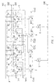
FIG. 1 is a circuit diagram showing a structure of the D-type flip-flop
circuit of the present embodiment. The structure thereof will be explained at
first with reference to the figure. A master circuit M comprises a first
differential circuit 1 for inputting data and a second differential circuit 2 for
holding data. A slave circuit S comprises a third differential circuit 3 for
inputting data and a fourth differential circuit 4 for holding data. Here, the first
differential circuit comprises transistors Q1 and Q2 whose emitters are
connected in common, whose collectors are connected to a source terminal VCC
via resistors R1 and R2, respectively, and whose bases receive signals from
terminals Din and VBB1 as data, respectively. It is noted that the signal from
the terminal VBB1 may be what is inverted from that from the terminal Din or
one of them may be a reference potential. Here, assuming that a reference
potential is applied to the terminal VBB1 and a current is being supplied to the
first differential circuit. Then, the transistors Q1 and Q2 are turned ON and
OFF, respectively, when the signal Din turns to "H" and are turned OFF and ON
when the signal turns to "L" which means "Low state" hereinafter. Thereby, the
transistors Q1 and Q2 are turned ON/OFF in response to the signal of the
terminal Din, so voltage drops due to the respective resistors R1 and R2 from the
potential of the source terminal VCC occur as outputs at the collectors,
respectively. These output data corresponding to the input data from the
terminal Din is written to terminals M1 and M2.
The second differential circuit 2 comprises transistors Q3 and Q4 whose
emitters are connected in common and whose bases and collectors are connected
across each other. The collector of the transistor Q3 and the base of the
transistor Q4 receive the data on the terminal M1 and the collector of the
transistor Q4 and the base of the transistor Q3 receive the data on the terminal
M2, thus holding and outputting the data while the current is being supplied.
A third differential circuit 3 and a fourth differential circuit 4 of the
slave circuit S are constructed in the same manner with the first differential
circuit 1 and the second differential circuit 2, respectively. Bases of the
transistors Q5 and Q6 of the third differential circuit 3 are connected with the
terminals M2 and M1, respectively, to receive the respective data and to write
output data corresponding to the output data from the second differential circuit
2 to terminals S1 and S2 connected to the respective collectors. Collectors of
transistors Q7 and Q8 of the fourth differential circuit 4 are connected
respectively with the terminals S1 and S2 which are provided with output
terminals OUT and OUT, respectively. It is noted that the terminals S1 and S2
are connected to the source terminal VCC via resistors R3 and R4.
A first current supplying circuit 5 supplies a current for the first and
third differential circuits 1 and 3 and a second current supplying circuit 6
supplies a current for the second and fourth differential circuits 2 and 4. Here,
although these circuits are constant-current circuits comprising transistors and
resistors similarly to the current supplying circuit shown in the aforementioned
prior art example, the present invention is not limited only to them and one
which is connected directly to a source terminal GND via a resistor may be
adopted.
A switching circuit 7 is a differential circuit comprising transistors Q9
and Q10 whose emitters are connected in common to the first current supplying
circuit 5, whose collectors are connected to emitter connecting points of the
respective transistors of the first differential circuits 1 and 3 and whose bases
are connected to clock terminals Cin1 and Cin1 to receive a first clock signal and
its inverted signal (or a reference potential) to supply the current alternately to
the first and third differential circuits 1 and 3.
A switching circuit 8 is a differential circuit comprising transistors Q11
and 12 whose emitters are connected in common to the second current supplying
circuit 6, whose collectors are connected to emitter connecting points of the
respective transistors of the second and fourth differential circuits 2 and 4 and
whose bases are connected to clock terminals Cin2 and Cin2 to receive a second
clock signal and its inverted signal (or a reference potential) to supply the
current alternately to the second and fourth differential circuits 2 and 4.
Here, the first clock signal is arranged so as to have a predetermined
delay with respect to the second clock signal. Thereby, a load in inverting data
is lightened by finishing the data holding operation of the second and fourth
differential circuits 2 and 4 earlier than causing the first and third differential
circuits 1 and 3 to perform the writing operation. Further, the inverting and
writing operations during writing may be also enhanced by starting the holding
operation of the second and fourth differential circuits 2 and 4 just before
finishing the writing operation of the first and third differential circuits 1 and 3.
Such a delay time is set by each circuit component and the like.
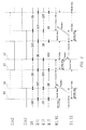
Next, an operation of the present embodiment will be explained based on
a 1/2 frequency dividing circuit as shown in FIG. 2 constructed by using the
D-type flip-flop circuit of the present embodiment. It is noted that the same
reference numerals in FIG. 2 with those shown in FIG. 1 denote the same
components with those in FIG. 1. The 1/2 frequency dividing circuit shown in
FIG. 2 is what the terminal Din is connected with the output terminal OUT and
the terminal VBB1 is connected with the terminal OUT in the D-type flip-flop
circuit shown in FIG. 1. Further, a terminal VBB2 is connected with the clock
terminals Cin1 and Cin2 to apply a common reference potential.
An operation of the 1/2 frequency dividing circuit shown in FIG. 2 will
be explained with reference to a timing chart shown in FIG. 3. Cin1 and Cin2 in
FIG. 3 represent first and second clock signals of the clock terminals Cin1 and
Cin2, Q9 through Q12 represent ON/OFF states of the respective transistors Q9
through Q12 and M1, M2, S1 and S2 represent data writing and holding states at
terminals M1 and M2 of the master circuit M and at terminals S1 and S2 of the
slave circuit S, respectively.
When the second clock signal turns to "H" at timing t0, the transistors
Q11 and Q12 are turned OFF and ON, respectively, stopping to supply the
current from the second current supplying circuit 6 to the second differential
circuit 2, and the data held in the terminals M1 and M2 are going to be vanished.
Further, as the transistor Q12 is turned ON, the current is started to be
supplied from the second current supplying circuit 6 to the fourth differential
circuit 4, So the operation for holding data in the terminals S1 and S2 is started.
Next, when the first clock signal turns to "H" at timing t1, the
transistors Q9 and Q10 of the first switching circuit 7 are turned ON and OFF,
respectively, thus starting to supply the current from the first current supplying
circuit 5 to the first differential circuit 1 and stopping to supply the current from
the first current supplying circuit 5 to the third differential circuit 3. The data
of the terminals S1 and S2 of the slave circuit S have been transmitted to the
first differential circuit 1, so that the operation for writing them to the terminals
M1 and M2 is started. For instance, when data "H" and "L" have been held in
the terminals M1 and M2, an operation for inverting them is carried out by
receiving the data of the terminals S1 and S2. However, because the data "H"
and "L" in the terminals M1 and M2 are on the way of being vanished from
timing t0, the load of the inverting operation at timing t1 is small, i.e. it becomes
possible to write quickly. The writing operation of the third differential circuit
3 stops as the first differential circuit 1 starts to write.
Next, when the second clock signal turns to "L" at timing t2, the
transistors Q11 and Q12 of the second switching circuit 8 are turned ON and
OFF, respectively, starting to supply the current from the second current
supplying circuit 6 to the second differential circuit 2 and stopping to supply the
current to the fourth differential circuit 4. Thereby, the second differential
circuit 2 starts to hold the data and, this holding operation and the writing
operation of the first differential circuit 1 combine to write the data strongly to
the terminals M1 and M2. In other words, the same data is written doubly.
When the supply of the current to the fourth differential circuit 4 is stopped, the
fourth differential circuit 4 stops the data holding operation and the data held in
the terminals S1 and S2 are going to be vanished.
Next, when the first clock signal turns to "L" at timing t3, the transistors
Q9 and Q10 of the first switching circuit 7 are turned OFF and ON, respectively,
thus stopping the data writing operation of the first differential circuit 1 and
starting the data writing operation of the third differential circuit 3. Further,
while the data held in the terminals M1 and M2 of the master circuit M are
transmitted to the third differential circuit 3, these data are transmitted
favorably because these data have been written doubly between timings t2 and
t3. Though the order of the explanation is reversed, the same can be said also in
transmitting the data from the slave circuit S to the master circuit M at timing
t1. Further, because the data held in the terminals S1 and S2 are on the way of
being vanished from timing t2, the data favorably transmitted are written
quickly. Thereafter, the series of operations at timings t0 through t3 are
repeatedly performed.
As described above, the writing operation can be performed steadily
because the old data is vanished before the new data is written both in the
master circuit M and the slave circuit S and the transmitting side writes the
same data doubly. These two actions allow the data to be transmitted favorably
which has been impossible in the prior art circuit, favorable output waveform to
be obtained and the 1/2 frequency dividing circuit to be operated at the high
operating frequency.
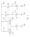
It is noted that while the operation of the present embodiment is made
possible by utilizing the propagation delay time, a data vanishing period
becomes too long and data is vanished when the delay between the first and
second clock signals is too large. It is no different from causing a clock skew.
Therefore, it is desirable to take the delay between the first and second clock
signals as a fixed value, not by frequency. A circuit as shown in FIG. 4 is used
for examples as such a delay stage. It is constructed as a differential circuit
comprising transistors Q13 and Q14 whose emitters are connected commonly to a
current supplying circuit 9, whose collectors are connected to the source
terminal VCC via resistors R5 and R6 and whose bases are applied with the
second clock signal and its inverted signal. A connecting point of the collector
of the transistor Q14 and the resistor R6 is connected to a base of a transistor
Q15 and an amplifier circuit (emitter-follower circuit) composed of the transistor
Q15 and a current supplying circuit 10 generates a signal from the terminal Cin1
as the first clock signal by receiving the state of the connecting point of the
collector and the resistor. Further, a connecting point of the collector of the
transistor Q13 and the resistor R5 is connected to a base of a transistor Q16 and
an amplifier circuit (emitter-follower circuit) composed of the transistor Q16 and
a current supplying circuit 11 generates an inverted signal of the first clock
signal from the terminal Cin1 by receiving the state of the connecting point of
the collector and the resistor. That is, the delay between the first and second
clock signals is decided by setting the delay of these amplifier circuits.
Next, a result of simulation carried out on the 1/2 frequency dividing
circuit shown in FIG. 2 will be described. The result of simulation carried out
on the 1/2 frequency dividing circuit using the prior art D-type flip-flop circuit
for the purpose of comparison will be also described. In concrete, one which
had been modified from the 1/2 frequency dividing circuit shown in FIG. 2 such
that the collector of the transistor Q10 is connected to the second differential
circuit 2, instead of the third differential circuit 3, the collector of the transistor
Q11 is connected to the third differential circuit 3, instead of the second
differential circuit 2, and the first clock signal is applied, instead of the second
clock signal, to the terminal Cin2 has been used as the prior art circuit as shown
in FIG. 5.
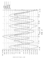
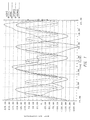
FIGs. 6 and 7 are waveform charts when the 1/2 frequency dividing
circuits in FIGs. 2 and 5 are operated with a clock signal of 1.25 GHz. A solid
line V[M1] in FIG. 6 represents an amplitude of voltage at the terminal M1 in
FIG. 2, an alternate dashed line V[CIN1] represents the first clock signal, a
dotted line V[CIN2] represents the second clock signal and a broken line V[M3]
represents an amplitude of voltage at the terminal M3 in FIG. 5. (The same
reference numerals refer to the same ones also in the waveform charts
hereinbelow.) A solid line V[S1] in FIG. 7 represents an amplitude of voltage at
the terminal S1 in FIG. 2 and a broken line V[S3] represents an amplitude of
voltage at the terminal S3 in FIG. 5. It is then apparent from the simulation
results shown in FIGs. 6 and 7 that the 1/2 frequency dividing circuit of the
present embodiment fully operates even with the clock signal in such high
frequency to which the prior art circuit cannot follow. That is, while the 1/2
frequency dividing circuit of the present embodiment can obtain the outputs
having clear waveforms as shown by the solid line V[M1] in FIG. 6 and the solid
line V[S1] in FIG. 7, the waveforms of the prior art 1/2 frequency dividing circuit
are distorted and are causing an erroneous operation as shown by the broken
line V[M3] in FIG. 6 and the broken line V[M3] in FIG. 7.
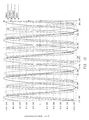
FIG. 8 shows a case when the 1/2 frequency dividing circuit is operated
with a clock signal of 1.1 GHz. This chart shows a comparative result when the
1/2 frequency dividing circuit of the present embodiment as well as that of the
prior art both follow the clock signal in the same manner. It can be seen from
the result of this chart that the 1/2 frequency dividing circuit of the present
embodiment can obtain an output having a clearer waveform having no
distortion.
FIG. 9 shows a case when the 1/2 frequency dividing circuit of the
present embodiment is operated with a clock signal of 1.4 GHz. As shown in the
chart, even the circuit of the present embodiment cannot follow such clock
signal in this case.
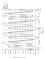
The above-mentioned simulation results have been obtained by
equalizing the value of the current supplied from the first and second current
supplying circuits 5 and 6 to the respective differential circuits as 50 µA. Then,
a simulation has been carried out on a case when the 1/2 frequency dividing
circuit is operated with the clock signal of 1.4 GHz by setting the value of
current of the first differential circuit 1 as 50 µA and that of the second current
supplying circuit 6 as 30 µA. As a result, it has been found that the 1/2
frequency dividing circuit operates even with the clock signal of 1.4 GHz as
shown in FIG. 10.
That is, the present invention is not limited only to the case when the
value of the current of the first current supplying circuit 5 is equalized with that
of the second current supplying circuit 6. Because it requires less value of
current on the level which will not vanish data in holding data like writing data
which is not involved with the inverting operation, it is possible to increase
operating frequency and to lessen power consumption by reducing the value of
the current of the second current supplying circuit 6 to be less than that of the
first current supplying circuit 5. The value of the current may be reduced by 20
% in the case of FIG. 10. Further, when a simulation has been carried out on a
case when the value of the current of the first current supplying circuit 5 is
increased more than that of the second current supplying circuit 6 without
changing the whole power consumption, it has been found that the 1/2 frequency
dividing circuit of the present embodiment operates even with the clock signal of
1.4 GHz as shown in FIG. 11. This arrangement excels in that a higher
amplitude of voltage can be obtained as compared to the case when the power
consumption is lowered. It is noted that the simulation shown in FIG. 11 has
been carried out by setting the value of the current of the first current supplying
circuit 5 at 60 µA and that of the second current supplying circuit at 40 µA.
As described above, with respect to the value of the current supplied
from the first and second current supplying circuits 5 and 6 to the respective
differential circuits, the present embodiment allows the operating frequency to
be increased and the value of power consumption to be reduced by setting the
value of the current of the second current supplying circuit 6 to be less than that
of the first current supplying circuit 5. It is noted that under the conditions of
the above-mentioned simulations, it has been possible to set the delay of the first
clock signal with respect to the second clock signal at 40 to 120 degrees, or
preferably 60 to 90 degrees, in terms of a phase lag.
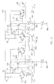
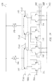
Next, another embodiment of the present invention will be described.
Part of the D-type flip-flop circuit of the first embodiment described
above may be altered as shown in FIG. 12. In the figure, the same reference
numerals with those in FIG. 2 refer to the same components. In the second
embodiment, emitter- follower circuits 12 and 13 are provided between the first
differential circuit 1 and the second differential circuit 2 and emitter- follower
circuits 14 and 15 are provided between the third differential circuit 3 and the
fourth differential circuit 4. That is, although there has been a case when
signals having a large amplitude are required depending on the latter circuit
using the signals of the terminals S1 and S2 in the circuit shown in FIG. 2, there
has been a fear that the operation is stopped and the amplitude could not be
increased so much because a current value might become too large when the
amplitude of the signal is increased too much and a base voltage VBE becomes
higher than a collector voltage VCE of a transistor receiving such current.
Then, in order to deal with such a case, the emitter-follower circuits 12 through
15 are provided in the present embodiment.
The emitter-follower circuit 12 comprises a transistor Q17 and a current
supplying circuit 16. A base of the transistor Q17 is connected to the collector of
the transistor Q1, a collector thereof is connected to the source terminal VCC
and an emitter thereof is connected to the current supplying circuit 16 as well as
to the base of the transistor Q4. The emitter-follower circuit 13 comprises a
transistor Q18 and a current supplying circuit 17. A base of the transistor Q18
is connected with the collector of the transistor Q2, a collector thereof is
connected with the source terminal VCC and an emitter thereof is connected
with the current supplying circuit 17 as well as with the base of the transistor
Q3.
That is, data is held through a route from the collector of the transistor
Q3 to the collector of the transistor Q1, the base emitter of the transistor Q17 and
the base of the transistor Q4 and a route from the collector of the transistor Q4
to the collector of the transistor Q2, the base emitter of the transistor Q18 and
the base of the transistor Q3. Thus, the respective holding routes contain the
emitter-follower circuits, so that one stage of the base voltage VBE may be
dropped between the first differential circuit 1 and the second differential circuit
2, eliminating the above-mentioned trouble.
The output to the third differential circuit 3 is sent from a connecting
point of the transistor Q17 and the current supplying circuit 16 and a connecting
point of the transistor Q18 and the current supplying circuit 17. The
emitter- follower circuits 14 and 15 also respectively comprise transistors Q19 and
Q20 and current supplying circuits 18 and 19 each connected in the same manner.
While an operation of the present embodiment will not be described specifically
in detail, the present embodiment shows almost the same action and effect with
those of the first embodiment. Further, because the emitter-follower circuits 12
through 15 are provided, an output having a large amplitude may be sent to the
latter circuits.
Further, although there have been two data input terminals (where, one
is used for inputting the reference potential or the inverted signal of the other
input data) in each embodiment described above, the present invention is not
limited only to such a case. For instance, it is possible to provide a transistor
Q21 in parallel to the transistor Q1 and to provide a data input terminal Din2 as
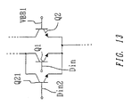
shown in FIG. 13 in order to operate a wired OR gate or the like.
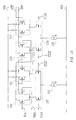
Still more, although all of the 1/2 frequency dividing circuits have been
composed of npn-type bipolar transistors in each embodiment described above,
the present invention is not limited only to such a case and the circuit may be
composed of pnp-type bipolar transistors. For instance, FIG. 14 shows a circuit
in which the pnp-type bipolar transistors are applied to the D-type flip-flop
circuit shown in FIG. 2. In this case, the circuit has the similar connection,
though the polarity of the power and current sources are inverted. It is noted
that the circuit comprises first through fourth differential circuits 141 through
144, first and second current supplying circuits 145 and 146 and first and second
switching circuits 147 and 148. It is noted that the data input terminal Din, the
clock terminal Cin1, the output terminal OUT and the like are shown in the
same manner with those shown in FIG. 2.
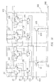
The inventive circuit may be constructed also by using MOS transistors,
instead of the bipolar transistors. For instance, FIG. 15 shows a case when the
circuit is constructed by using N channel MOS transistors. In the figure, the
circuit comprises first through fourth differential circuits 151 through 154, first
and second current supplying circuits 155 and 156 and first and second switching
circuits 157 and 158. It is noted that the data input terminal Din, the clock
terminal Cin1, the output terminal OUT and the like are shown in the same
manner with those shown in FIG. 2. The inventive circuit may be constructed
by using P channel MOS transistors, instead of the N channel MOS transistors,
also in the circuit composed of the MOS transistors in FIG. 15. Although its
example is not shown specifically, the circuit has the same connection with that
composed of the N channel MOS transistors, though the polarity of the power
and current sources are inverted, similarly to the above-mentioned case of the
bipolar transistors.
As described above, according to the invention, the operation timing of
the differential circuits for inputting data and for holding data is optimized by
dividing the current supplying source to the respective two differential circuits
for inputting data (first and third differential circuits) and for holding data
(second and fourth differential circuits) of the master circuit and slave circuit,
by controlling the timing for supplying the current separately by the first and
second clock signals and by arranging the first clock signal so as to have the
predetermined delay with respect to the second clock signal. Accordingly, the
remarkable effects can be obtained in the aspects of the operating frequency, the
waveform in operating in high frequency and the ability for transmitting data.
In addition to that, it is possible to increase the operating frequency further
and to lower the power consumption by setting the value of the current supplied
to the second and fourth differential circuits to be less than that supplied to the
first and third differential circuits.
While the preferred embodiments have been described, variations
thereto will occur to those skilled in the art within the scope of the present
inventive concepts which are delineated by the following claims.