EP0876918A2 - Electrostatic writing head for an electronic printing machine - Google Patents
Electrostatic writing head for an electronic printing machine Download PDFInfo
- Publication number
- EP0876918A2 EP0876918A2 EP98106393A EP98106393A EP0876918A2 EP 0876918 A2 EP0876918 A2 EP 0876918A2 EP 98106393 A EP98106393 A EP 98106393A EP 98106393 A EP98106393 A EP 98106393A EP 0876918 A2 EP0876918 A2 EP 0876918A2
- Authority
- EP
- European Patent Office
- Prior art keywords
- dielectric
- electrostatic
- printing machine
- plasma
- electrode
- Prior art date
- Legal status (The legal status is an assumption and is not a legal conclusion. Google has not performed a legal analysis and makes no representation as to the accuracy of the status listed.)
- Granted
Links
Images


Classifications
-
- B—PERFORMING OPERATIONS; TRANSPORTING
- B41—PRINTING; LINING MACHINES; TYPEWRITERS; STAMPS
- B41J—TYPEWRITERS; SELECTIVE PRINTING MECHANISMS, i.e. MECHANISMS PRINTING OTHERWISE THAN FROM A FORME; CORRECTION OF TYPOGRAPHICAL ERRORS
- B41J2/00—Typewriters or selective printing mechanisms characterised by the printing or marking process for which they are designed
- B41J2/385—Typewriters or selective printing mechanisms characterised by the printing or marking process for which they are designed characterised by selective supply of electric current or selective application of magnetism to a printing or impression-transfer material
- B41J2/39—Typewriters or selective printing mechanisms characterised by the printing or marking process for which they are designed characterised by selective supply of electric current or selective application of magnetism to a printing or impression-transfer material using multi-stylus heads
- B41J2/395—Structure of multi-stylus heads
Definitions
- the present invention relates generally to miniature loaders for application a controlled amount of electrical charge on a receptor.
- the invention relates to a write head for an electronic printing machine.
- Some charging devices use corona discharge or arc discharge applied to generate charge carriers. Such devices suffer from one locally very specific and sporadic electron leakage from a cathode, what that Controlling the charging process difficult. It is also difficult to have a high plasma space loading density maintain and thus the possible cathode current density reduce.
- the charge carriers are generated in a direct current glow plasma.
- a direct current glow plasma Although such devices create a denser, more conductive plasma than corona devices, it is a disadvantage that the cathode still has to be exposed to the plasma. Due to the surface condition of the cathode, functional fluctuations and edge effects, uneven current distributions and electrical fields appear on the cathode surface. These uneven current distributions and electric fields cause a time-related fluctuation pattern of hot spots "on the cathode surface, which is generally indicated by the hot spots ", sputtering and glow-electric evaporation lead to rapid erosion. Furthermore, chemically reactive types of charge carriers generated in the plasma (in particular if the plasma is generated in air) can decompose or oxidize the electrode exposed to the plasma. These effects can cause life of such a device, and these devices require a gas-containing environment and a complicated, controlled gas delivery system to form the appropriate plasma.
- High frequency discharge is used in other charging devices.
- the Strength of the transferred charge is controlled by the length of time that the Discharge ignited, controlled as described in US 4,992,807. This has the disadvantage that the high-frequency source must be given pulses and thus the plasma is repeatedly ignited and cooled.
- Toshiba Corporation also has one Ion beam "- ( ion-jet ") - Printhead in which two electrodes are used on both sides of a ceramic layer in connection with an alternating voltage supply.
- this printhead is used to apply large amounts of charge, it is not a writing head and therefore cannot be individual, corresponding to a picture element
- a separate control electrode is required on both sides of the ceramic layer, and no control electrode is provided directly on the ceramic layer.
- charge carriers are caused by a high-frequency gas discharge generated.
- the electrode that sends the radio frequency signal is on one One side of a dielectric body is arranged, and the discharge is on a second one Side ignited.
- the high-frequency electrode is therefore not exposed to the plasma.
- a control electrode is provided on the second side of the dielectric body causes a controlled amount of electrical charge to the receptor, e.g. B. one Printing cylinder in a printing press, is transferred.
- a high frequency source is applied to a High-frequency electrode applied to generate a plasma on a first Side of the dielectric body is arranged.
- a variety of control electrodes are arranged on the second side of the dielectric body and ensure that correct loads.
- the voltage at the high-frequency electrode is sufficiently high, it ignites near the second side of the dielectric body a plasma, the electron, negative contains charged ions and positively charged ions.
- the plasma control signals are sent to the plurality of control electrodes.
- the average voltage of the plasma in the vicinity of the control electrode changes by the value of the control signal, but the state of the plasma remains basically unaffected with regard to its earth potential.
- the receptor is e.g. B. a printing cylinder with a dielectric layer, which are on a grounded layer or on a charged with a constant voltage Layer supports. The charging of the receptor continues until it is on Potential that is equal to the potential of the control electrode is charged. To At this point, the ions in the plasma will no longer go towards the receptor dressed.
- the device of the present invention can because of the excellent Plasma formation, which is achieved by the high-frequency electrode, advantageously and preferably used in ordinary atmospheric pressure environments will.
- the device is also for operation in an atmosphere that is gas (e.g. argon, nitrogen or gas-air mixtures), the supply of which is controlled, suitable.
- gas e.g. argon, nitrogen or gas-air mixtures
- the use of ordinary atmospheric air simplifies use of the print head is essential, whereas a controlled gas atmosphere, which is suitable for some prior art devices are needed, a complicated one Gas supply system required and also to crosstalk between the control electrodes arranged side by side leads. This crosstalk is in ordinary atmospheric environment diminished or almost eliminated because the average free range of plasma ions is quite short.
- the loading devices are advantageously, but not necessarily, arranged in a row side by side.
- An arrangement of these devices can be used as an electrostatic write head with a printing press. With such use, the receptor would be the surface of a cylinder of the printing press. With such an arrangement of charging devices, pixels are written on the printing cylinder, which have a grid spacing of approximately 50 ⁇ m and a charging current density of approximately 1 mA / cm 2 and are suitable for fast electrostatic writing, with a gray scale at a speed in the range of approx. 1 m / s.
- Fig. 1 shows a side view along the length of an embodiment of the present invention, in which a continuous, sinusoidal High frequency source 1 from 800 to 3000 volts from peak to peak at 4 kHz to 1 MHz is applied to a high-frequency electrode 2. Except for contact with the High-frequency source 1, the electrode 2 is encased and supported by a suitable one dielectric medium or an insulating substrate (not shown) or on top of it built to prevent parasitic electronic discharges from the electrode.
- the high-frequency electrode 2 is along a first side 3 of a dielectric Body 4 of usually 10 microns to 100 microns thick arranged.
- the electrode 2 Preferably extends the electrode 2 extends along the entire width of the dielectric body 4.
- One Control electrode 5, for example 10 microns to 50 microns wide and one of a Variety of control electrodes is on the second side 6 of the dielectric Body 4 arranged.
- the control electrode 5 is capacitively grounded. Here is this Grounding through the capacitor 8 is shown schematically, for example with a Capacitance from 3 to 100 pF.
- a resistor 7, the z. B. a resistance value of 1 mega-ohm can be used to provide a control signal source 10 To protect against current surges.
- the control electrode 5 is positioned so that a Overlap is just avoided or so that this is the horizontal position of the High-frequency electrode 2 overlapped more or less.
- the dielectric body 4 should be free of pinholes and resistant to the formation of pinholes during operation. Puncture holes in the dielectric body 4 can cause a strong direct current to flow through the dielectric body, which disrupts the control mechanism and causes physical damage in the area of the puncture holes.
- the dielectric body 4 can have several layers of dielectric material because the layer construction prevents growth disorders from spreading through the entire thickness of the dielectric body 4. A natural mica, 30 ⁇ m thick and of course comprising several layers, has shown excellent durability, even if the atmosphere used for the plasma was air.
- An artificial dielectric body 4 with one or more layers of dielectric material can be created by layering or laminating the same dielectric material or by alternating layers of different materials. Such dielectric materials can include KAPTAN-PR, a polyimide manufactured by DuPont, glass and other common dielectric films such as. B. SiO 2 or Al 2 O 3 .
- the high-frequency electrode 2 preferably works at 4 kHz to 400 kHz or above; at this frequency a stable plasma is formed, that can tolerate fluctuating control voltages.
- a control signal 10 is issued while this state of the plasma is being maintained in the range of -600 V to + 600 V to the control electrode 5.
- the DC voltage via the dielectric body 4 in the vicinity of the control electrode 5 changes by the value of the voltage generated by the control signal source 10, however apart from its earth potential, the state of the plasma 9 remains unaffected. Consequently when the control signal 10 is applied, the appearance of the plasma 9 (in its size, color, brightness, etc.) little.
- the ground connections of the high-frequency source 1 and the control signal source 10 are connected to the Ground connection of a conductive reference electrode 11 (for example a grounded layer) a receptor 12, the surface 13 of which must be charged, connected. This is true e.g. B. towards a printing cylinder surface. If the receptor 12 is close to the plasma 9 comes up, the surface 13 is charged to a potential that the Voltage potential at the control electrode 5 corresponds. Under normal Operating conditions fluctuate the actual potential of the receptor surface 13 in an almost linear relationship to that applied to the control electrode 5 Voltage, but offset by an offset voltage.
- the offset voltage for a particular system is 30 volts and then a voltage of minus 30 volts is applied by the control signal source 10 surface 13 is charged up to a zero potential or earth potential. If a voltage of 70 volts is applied by the control signal source 10, then the Surface 13 charged to a potential of approximately 100 volts.
- the difference or Offset voltage between the voltage of the control signal source 10 and that at the Surface 13 applied potential is advantageously within a Voltage range of +/- 300 volts pretty constant.
- the offset voltage can be used for a certain construction, e.g. B. a printing press, measured and for calculation the desired control signal voltages that are required for a desired potential at the Surface 13 must be created, are used. If the offset voltage is constant, this calculation is a simple step of addition or subtraction.
- the charging device of the present invention thus enables accurate Process of applying a charge to a receptor over a wide range of tensions.
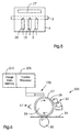
- FIG. 7 schematically shows a system for calculating the charging current, I OUT , of the charging device of FIG. 1, in which the charging current is applied to a surface from a specific distance d (as shown).
- This system can also be used to calculate the offset voltage described above.
- a test electrode 111 is connected to a screen 115, on which the charging current is then displayed, namely through the resistance element 117, which, for. B. has a resistance of 100 kilohms.
- a capacitor 118 with a low capacitance, for example with a capacitance of 0.1 microfarads, can also be connected in the manner shown. Since the control voltage V c , which is grounded and coupled to a capacitor 119 (e.g.
- the charging current is measured by the oscillograph .
- the width of the test electrode (as shown in FIG. 7) can be expanded to a width that equals a pixel width multiplied by a factor m, where a single control voltage is applied to a plurality of control electrodes.
- the charging current for an individual control electrode, the width of which is equal to a pixel width, can then be calculated by dividing the measured charging current by the factor m.
- the charging current blackens from a distance d of 0.25 mm almost linear with the voltage applied to the control electrode 5.
- the charging current is approximately zero, which is equivalent to the fact that no charge is applied to the receptor surface. It is charging current of higher values is also available if the distance d is reduced and / or the high-frequency voltage is increased.
- Other options such as B. measuring the actual charge or Potential applied to the receptor surface and measuring its surface temporal reactions are equally valid.
- the loading devices of the present invention for use as a write head 100 in a printing press are advantageously arranged in a side-by-side row.
- a plurality of control electrodes 5, 15 and 25 are arranged on the second side 6 of a single dielectric body 4.
- Each of the control electrodes 5, 15, 25, etc. has an independent control signal V C1 , V C2 , V C3 , etc.
- the end faces of the control electrodes 5, 15, 25 are typically oriented at an angle of 90 ° with respect to the high-frequency electrode 2. In such an arrangement of the charging devices, crosstalk between the control electrodes 5, 15, and 25 can be reduced by installing insulating structures.
- control electrodes can be coated with a layer of dielectric Material are coated, only the ends of the control electrodes, which the Nearest plasma are left uncoated.
- the process in Atmospheric air takes place as is preferred, be such insulating Constructions are hardly necessary.
- an insulating construction 24 with an open end is provided to reduce cross-coupling between the control electrodes 5, 15 and 25.
- This open ended insulating structure 24 can be a ribbed cover made of dielectric material. It can also be a conductive transducer or a protective electrode which, for. B. is connected to a constantly charged source and absorbs scattered ions or shovels "or holds the ion flow.
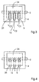
- Fig. 4 is another embodiment in which an insulating or conductive Construction 26 is provided with a closed end.
- This isolating Construction 26 can also be a ribbed cover made of dielectric material or be a pickup or a protective electrode.
- a transducer or a Protective electrode 27 at the opposite ends of the Control electrodes 5, 15, 25 may be placed to reduce crosstalk.
- the write head 100 of the present invention is as a component of a electrostatic printing machine 200 shown.
- a mass storage device 210 can do that Save data representing the image to be printed, including the gray scale data.
- the Processor 205 provides the correct voltage for each control electrode of the Printhead 100 according to the data representing the image to be printed.
- a Pressure organ, d. H. an impression cylinder 26 has a dielectric surface 27 which serves as a receptor.
- the dielectric surface 27 is on a conductive Layer 28, which serves as a conductive reference electrode and a grounded layer or a layer set by a controller to a certain constant voltage can be.
- the write head 100 is in the vicinity of the dielectric surface 27 of the Printing cylinder 26 arranged, and the individual control electrodes extend along the length of the write head 100.
- the write head 100 is similar to that in FIG. 2 shown type, however, the write head in Fig. 2 is reversed, so that the plasma 9th contacts the dielectric surface 27.
- the pressure cylinder 26 rotates in the direction indicated; the moves dielectric surface 27 of the printing cylinder 26 close to the write head 100.
- the Control processor 205 sends control signals to the plurality of control electrodes which are contained in the write head 100 in order to achieve the charged pixels on the dielectric surface 27 of the printing cylinder 26 to record so that a latent image arises.
- the dielectric Surface 27 After the dielectric Surface 27 has passed the print head 100 and received charges from it, it passes a color source 32.
- this color source 32 consists of two Ink rollers that are connected to an ink fountain, however, can also be any other color source can be used. Color, as it is to be defined here, exists both from liquid colors and from dry toner.
- a Printing substrate 34 e.g. B. a paper spell or a sheet of paper in contact.
- the Print substrate 34 may be in contact with dielectric surface 27 through a Impression cylinder 35 are held in a suitable position. At the contact point transfer the color to the printing substrate 34 and thus the image 36 to the Print substrate 34 printed.
- the dielectric surface 27 then passes through one Extinguishing device 37, e.g. B. a source of ultraviolet light.
- the present invention also applies to copying machines and Fax machines that are here under the definition of electrostatic printing presses included, can be used.
- the invention is also for a four-color printing press usable, in which each of four printing cylinders one Has printhead and the four printheads by a common Control processor can be controlled.
Abstract
Description
Die vorliegende Erfindung betrifft generell Miniatur-Ladevorrichtungen zum Aufbringen einer gesteuerten Größe einer elektrischen Ladung auf einen Rezeptor. Im besonderen betrifft die Erfindung einen Schreibkopf für eine elektronische Druckmaschine.The present invention relates generally to miniature loaders for application a controlled amount of electrical charge on a receptor. In particular The invention relates to a write head for an electronic printing machine.
Bei manchen Ladevorrichtungn wird eine Koronaentladung oder Lichtbogenentladung angewandt, um Ladungsträger zu erzeugen. Solche Vorrichtungen leiden unter einem örtlich sehr spezifischen und sporadischen Elektronenaustritt aus einer Kathode, was das Steuern des Ladeprozesses erschwert. Es ist auch schwierig, eine hohe Plasmaraum-Ladedichte aufrechtzuerhalten und somit die mögliche Kathodenstromdichte zu verringern.Some charging devices use corona discharge or arc discharge applied to generate charge carriers. Such devices suffer from one locally very specific and sporadic electron leakage from a cathode, what that Controlling the charging process difficult. It is also difficult to have a high plasma space loading density maintain and thus the possible cathode current density reduce.
In anderen Ladevorrichtungen werden die Ladungsträger in einem Gleichstrom-Glühplasma
erzeugt. Obschon solche Vorrichtungen ein dichteres, besser leitendes
Plasma als Korona-Einrichtungen schaffen, ist es ein Nachteil, daß die Kathode dem
Plasma noch ausgesetzt werden muß. Aufgrund der Oberflächenbeschaffenheit der
Kathode treten an der Kathodenoberfläche Funktionsschwankungen und Randeffekte,
ungleichmäßige Stromaufteilungen und elektrische Felder in Erscheinung. Diese
ungleichmäßigen Stromaufteilungen und elektrischen Felder verursachen ein
zeitbezogenes Schwarkungsmuster von ![]()
![]()
In weiteren Ladevorrichtungen wird eine Hochfrequenz-Entladung angewandt. Die Stärke der übertragenen Ladung wird gesteuert, indem die Länge der Zeit, in der sich die Entladung entzündet, gesteuert wird, wie dies in US 4,992,807 beschrieben ist. Dies hat den Nachteil, daß der Hochfrequenzquelle Impulse gegeben werden müssen und somit das Plasma wiederholt entzündet und abgekühlt wird.High frequency discharge is used in other charging devices. The Strength of the transferred charge is controlled by the length of time that the Discharge ignited, controlled as described in US 4,992,807. this has the disadvantage that the high-frequency source must be given pulses and thus the plasma is repeatedly ignited and cooled.
Die Toshiba Corporation hat auch einen
Gemäß der vorliegenden Erfindung werden Ladungsträger durch eine Hochfrequenz-Gasentladung erzeugt. Die Elektrode, die das Hochfrequenzsignal sendet, ist auf einer Seite eines dielektrischen Körpers angeordnet, und die Entladung wird auf einer zweiten Seite entzündet. Somit ist die Hochfrequenz-Elektrode dem Plasma nicht ausgesetzt. Auf der zweiten Seite des dielektrischen Körpers ist eine Steuerungselektrode vorgesehen, die bewirkt, daß eine gesteuerte Größe an elektrischer Ladung auf den Rezeptor, z. B. einen Druckzylinder in einer Druckmaschine, übertragen wird.According to the present invention, charge carriers are caused by a high-frequency gas discharge generated. The electrode that sends the radio frequency signal is on one One side of a dielectric body is arranged, and the discharge is on a second one Side ignited. The high-frequency electrode is therefore not exposed to the plasma. On A control electrode is provided on the second side of the dielectric body causes a controlled amount of electrical charge to the receptor, e.g. B. one Printing cylinder in a printing press, is transferred.
In der Vorrichtung der vorliegenden Erfindung wird eine Hochfrequenzquelle auf eine Hochfrequenz-Elektrode angewandt, die zur Erzeugung eines Plasmas auf einer ersten Seite des dielektrischen Körpers angeordnet ist. Eine Vielzahl von Steuerungselektroden sind auf der zweiten Seite des dielektrischen Körpers angeordnet und sorgen für die korrekten Ladungen.In the device of the present invention, a high frequency source is applied to a High-frequency electrode applied to generate a plasma on a first Side of the dielectric body is arranged. A variety of control electrodes are arranged on the second side of the dielectric body and ensure that correct loads.
Wenn die Spannung an der Hochfrequenz-Elektrode ausreichend hoch ist, entzündet sich nahe der zweiten Seite des dielektrischen Körpers ein Plasma, das Elektronen, negativ geladene Ionen und positiv geladene Ionen enthält. Während das Plasma aufrechterhalten wird, ergehen Steuersignale an die Vielzahl der Steuerungselektroden. Die durchschnittliche Spannung des Plasmas in der Umgebung der Steuerungselektrode ändert sich um den Wert des Steuersignals, jedoch bleibt der Zustand des Plasmas außer im Hinblick auf sein Erdpotential grundsätzlich unbeeinflußt.If the voltage at the high-frequency electrode is sufficiently high, it ignites near the second side of the dielectric body a plasma, the electron, negative contains charged ions and positively charged ions. While maintaining the plasma control signals are sent to the plurality of control electrodes. The average voltage of the plasma in the vicinity of the control electrode changes by the value of the control signal, but the state of the plasma remains basically unaffected with regard to its earth potential.
Wenn ein geeigneter Rezeptor in die Nähe des Plasmas gebracht wird, dann werden die Ionen in dem Plasma von dem Rezeptor angezogen und bewirken somit die Aufladung des Rezeptors. Der Rezeptor ist z. B. ein Druckzylinder mit einer dielektrischen Schicht, die sich auf eine geerdete Schicht oder auf eine mit einer konstanten Spannung geladenen Schicht stützt. Das Laden des Rezeptors wird solange fortgesetzt, bis dieser auf ein Potential, das dem Potential der Steuerungselektrode gleichkommt, aufgeladen ist. Zu diesem Zeitpunkt werden die Ionen in dem Plasma nicht mehr in Richtung des Rezeptors angezogen.If a suitable receptor is brought close to the plasma, then the Ions in the plasma are attracted to the receptor and thus cause charging of the receptor. The receptor is e.g. B. a printing cylinder with a dielectric layer, which are on a grounded layer or on a charged with a constant voltage Layer supports. The charging of the receptor continues until it is on Potential that is equal to the potential of the control electrode is charged. To At this point, the ions in the plasma will no longer go towards the receptor dressed.
Die Vorrichtung der vorliegenden Erfindung kann aufgrund der ausgezeichneten Plasmabildung, die durch die Hochfrequenz-Elektrode erzielt wird, in vorteilhafter Weise und bevorzugt in gewöhnlicher Umgebung mit atmosphärischem Druck eingesetzt werden. Die Vorrichtung ist aber auch für den Betrieb in einer Atmosphäre, die Gas (z. B. Argon, Stickstoff oder Gas-Luft-Mischungen) enthält, dessen Zufuhr gesteuert ist, geeignet. Die Nutzung der gewöhnlichen atmosphärischen Luft vereinfacht den Einsatz des Schreibkopfes ganz wesentlich, wohingegen eine gesteuerte Gasatmosphäre, die für einige Vorrichtungen des Standes der Technik benötigt wird, ein kompliziertes Gaszuführsystem erfordert und außerdem zum Übersprechen zwischen den nebeneinander angeordneten Steuerungselektroden führt. Dieses Übersprechen ist in gewöhnlicher atmosphärischer Umgebung vermindert oder beinahe beseitigt, weil die durchschnittliche freie Strecke der Plasma-Ionen ziemlich kurz ist.The device of the present invention can because of the excellent Plasma formation, which is achieved by the high-frequency electrode, advantageously and preferably used in ordinary atmospheric pressure environments will. The device is also for operation in an atmosphere that is gas (e.g. argon, nitrogen or gas-air mixtures), the supply of which is controlled, suitable. The use of ordinary atmospheric air simplifies use of the print head is essential, whereas a controlled gas atmosphere, which is suitable for some prior art devices are needed, a complicated one Gas supply system required and also to crosstalk between the control electrodes arranged side by side leads. This crosstalk is in ordinary atmospheric environment diminished or almost eliminated because the average free range of plasma ions is quite short.
Die Ladevorrichtungen sind vorteilhafterweise, jedoch nicht notwendigerweise in einer Reihe Seite an Seite angeordnet. Eine Anordnung dieser Vorrichtungen kann als elektrostatischer Schreibkopf mit einer Druckmaschine verwendet werden. Bei solch einer Verwendung würde der Rezeptor die Oberfläche eines Zylinders der Druckmaschine sein. Mit solch einer Anordnung von Ladevorrichtungen werden Bildpunkte auf den Druckzylinder geschrieben, die einen Rasterabstand von ca. 50 µm und eine Ladestromdichte von ca. 1 mA/cm2 aufweisen und zum schnellen elektrostatischen Schreiben geeignet sind, wobei sich eine Grauskala bei einer Geschwindigkeit im Bereich von ca. 1 m/s ergibt.The loading devices are advantageously, but not necessarily, arranged in a row side by side. An arrangement of these devices can be used as an electrostatic write head with a printing press. With such use, the receptor would be the surface of a cylinder of the printing press. With such an arrangement of charging devices, pixels are written on the printing cylinder, which have a grid spacing of approximately 50 μm and a charging current density of approximately 1 mA / cm 2 and are suitable for fast electrostatic writing, with a gray scale at a speed in the range of approx. 1 m / s.
Die Vorteile und Merkmale der vorliegenden Erfindung werden in der folgenden Beschreibung im Zusammenhang mit den beigefügten, nachstehend aufgeführten Zeichnungen näher erläutert.The advantages and features of the present invention are as follows Description related to the attached, listed below Drawings explained in more detail.
Es zeigen:
- Fig. 1
- eine Querschnittansicht einer Ausführungsform der Erfindung;
- Fig. 2
- eine Draufsicht der in Fig. 1 gezeigten Ausführungsform der Erfindung;
- Fig. 3
- eine Draufsicht einer weiteren Ausführungsform der Erfindung;
- Fig. 4
- eine Draufsicht einer weiteren Ausführungsform der Erfindung;
- Fig. 5
- eine Draufsicht einer weiteren Ausführungsform der Erfindung;
- Fig. 6
- eine Ansicht einer elektrostatischen Druckmaschine, in welcher die erfindungsgemäße Vorrichtung als Schreibkopf verwendet wird;
- Fig. 7
- eine Vorrichtung zum Messen der elektronischen Eigenschaften eines elektrostatischen Druckmaschinensystems;
- Fig. 8
- die Output-Eigenschaften eines vereinfachten Druckmaschinensystems.
- Fig. 1
- a cross-sectional view of an embodiment of the invention;
- Fig. 2
- a plan view of the embodiment of the invention shown in Fig. 1;
- Fig. 3
- a plan view of another embodiment of the invention;
- Fig. 4
- a plan view of another embodiment of the invention;
- Fig. 5
- a plan view of another embodiment of the invention;
- Fig. 6
- a view of an electrostatic printing machine in which the device according to the invention is used as a write head;
- Fig. 7
- a device for measuring the electronic properties of an electrostatic printing press system;
- Fig. 8
- the output properties of a simplified press system.
Fig. 1 zeigt eine Seitenansicht entlang der Länge einer Ausführungsform der
vorliegenden Erfindung, in welcher eine kontinuierliche, sinusförmig verlaufende
Hochfrequenzquelle 1 von 800 bis 3000 Volt von Spitze zu Spitze bei 4 kHz bis 1 MHz
auf eine Hochfrequenz-Elektrode 2 angewandt wird. Außer für den Kontakt mit der
Hochfrequenzquelle 1 ist die Elektrode 2 ummantelt und gestützt von einem geeigneten
dielektrischen Medium oder einem isolierenden Substrat (nicht gezeigt) oder auf diesem
aufgebaut, um parasitäre elektronische Entladungen von der Elektrode zu verhindern.
Die Hochfrequenz-Elektrode 2 ist entlang einer ersten Seite 3 eines dielektrischen
Körpers 4 von gewöhnlich 10 µm bis 100 µm Dicke angeordnet. Vorzugsweise erstreckt
sich die Elektrode 2 entlang der gesamten Breite des dielektrischen Körpers 4.Eine
Steuerungselektrode 5, die beispielsweise 10 µm bis 50 µm breit und eine von einer
Vielzahl von Steuerungselektroden ist, ist auf der zweiten Seite 6 des dielektrischen
Körpers 4 angeordnet. Die Steuerungselektrode 5 ist kapazitiv geerdet. Hier ist diese
Erdung durch den Kondensator 8 schematisch dargestellt, beispielsweise mit einer
Kapazität von 3 bis 100 pF. Ein Widerstand 7, der z. B. einen Widerstandswert von
1 Mega-Ohm aufweist, kann verwendet werden, um eine Steuersignalquelle 10 vor
Stromspitzenstößen zu schützen. Die Steuerungselektrode 5 ist so positioniert, daß eine
Überlappung gerade vermieden wird oder so, daß diese die horizontale Position der
Hochfrequenz-Elektrode 2 mehr oder weniger überlappt.Fig. 1 shows a side view along the length of an embodiment of the
present invention, in which a continuous, sinusoidal
High frequency source 1 from 800 to 3000 volts from peak to peak at 4 kHz to 1 MHz
is applied to a high-
Der dielektrische Körper 4 sollte frei von Punkturlöchern und gegen die Bildung von
Punkturlöchern während des Betriebs resistent sein. Durch Punkturlöcher im
dielektrischen Körper 4 kann es dazu kommen, daß ein starker Gleichstrom durch den
dielektrischen Körper fließt, der den Steuermechanismus stört und physischen Schaden
im Bereich der Punkturlöcher verursacht. Der dielektrische Körper 4 kann mehrere
Schichten von dielektrischem Material aufweisen, weil die Schichtenkonstruktion
verhindert, daß sich Zuwachsstörungen durch die gesamte Dicke des dielektrischen
Körpers 4 hin ausbreiten können. Ein natürlicher Glimmer, der 30 µm dick ist und
selbstverständlich mehrere Schichten umfaßt, hat ausgezeichnete Dauerhaftigkeit gezeigt,
auch wenn die für das Plasma benutzte Atmosphäre Luft gewesen ist. Ein künstlicher
dielektrischer Körper 4 mit einem oder mehreren Schichten von dielektrischem Material
kann durch Aufschichten oder Laminieren des gleichen dielektrischen Materials oder
durch wechselnde Schichten verschiedener Materialien geschaffen werden. Solche
dielektrischen Materialien können KAPTAN-PR, ein von DuPont hergestelltes Polyimid,
Glas und andere übliche dielektrische Filme, wie z. B. SiO2 oder Al2O3, sein.The
Wenn die Spannung an der Hochfrequenzelektrode 2 hoch genug ist, wird ein Plasma 9,
das Elektronen und positiv geladene Ionen enthält, nahe der zweiten Seite 6 des
dielektrischen Körpers 4 entzündet. Vorzugsweise arbeitet die Hochfrequenz-Elektrode
bei 4 kHz bis 400 kHz oder darüber; bei dieser Frequenz bildet sich ein stabiles Plasma,
das schwankende Steuerungsspannungen tolerieren kann.If the voltage at the high-
Während dieser Zustand des Plasmas aufrechterhalten wird, ergeht ein Steuersignal 10
im Bereich von -600 V bis + 600 V an die Steuerungselektrode 5. Die Gleichstrom-Spannung
über den dielektrischen Körper 4 in der Umgebung der Steuerungselektrode 5
ändert sich um den Wert der von der Steuersignalquelle 10 erzeugten Spannung, jedoch
der Zustand des Plasmas 9 bleibt abgesehen von seinem Erdpotential unbeeinflußt. Somit
ändert sich beim Anbringen des Steuersignals 10 das Erscheinungsbild des Plasmas 9 (in
seinem Ausmaß, in der Farbe, in der Helligkeit, usw.) wenig.A
Die Erdanschlüsse der Hochfrequenzquelle 1 und der Steuersignalquelle 10 sind mit dem
Erdanschluß einer leitenden Bezugselektrode 11 (beispielsweise einer geerdeten Schicht)
eines Rezeptors 12, dessen Oberfläche 13 aufgeladen werden muß, verbunden. Dies trifft
z. B. auf eine Druckzylinderoberfläche zu. Wenn der Rezeptor 12 nahe an das Plasma 9
herankommt, wird die Oberfläche 13 bis zu einem Potential aufgeladen, die dem
Spannungspotential an der Steuerungselektrode 5 entspricht. Unter normalen
Betriebsbedingungen schwankt das eigentliche Potential der Rezeptoroberfläche 13 in
einem nahezu linearen Verhältnis zu der an der Steuerungselektrode 5 angelegten
Spannung, jedoch um eine Offsetspannung versetzt.The ground connections of the high-frequency source 1 and the
Wenn beispielsweise die Offsetspannung für ein bestimmtes System 30 Volt beträgt und
durch die Steuersignalquelle 10 eine Spannung von minus 30 Volt angelegt wird, dann
wird die Oberfläche 13 bis zu einem Null-Potential oder Erdpotential aufgeladen. Wenn
durch die Steuersignalquelle 10 eine Spannung von 70 Volt angelegt wird, dann wird die
Oberfläche 13 bis zu einem Potential von ca. 100 Volt aufgeladen. Die Differenz oder
Offsetspannung zwischen der Spannung der Steuersignalquelle 10 und dem an der
Oberfläche 13 angelegten Potential ist vorteilhafterweise innerhalb eines
Spannungsbereichs von +/-300 Volt ziemlich konstant. Die Offsetspannung kann für
eine bestimmte Konstruktion, z. B. eine Drucktnaschine, gemessen und zur Berechnung
der gewünschten Steuersignalspannungen, die für ein gewünschtes Potential an der
Oberfläche 13 angelegt werden müssen, verwendet werden. Wenn die Offsetspannung
konstant ist, so ist diese Berechnung ein einfacher Schritt der Addition oder Subtraktion.For example, if the offset voltage for a particular system is 30 volts and
then a voltage of minus 30 volts is applied by the
Die Ladevorrichtung der vorliegenden Erfindung ermöglicht somit ein akkurates Verfahren des Aufbringens einer Ladung auf einen Rezeptor über einen weiten Bereich von Spannungen.The charging device of the present invention thus enables accurate Process of applying a charge to a receptor over a wide range of tensions.
Fig. 7 zeigt schematisch ein System zum Berechnen des Ladestroms, IOUT, der
Ladevorrichtung der Fig. 1, in welchem der Ladestrom aus einem bestimmten Abstand d
(wie gezeigt) auf eine Oberfläche aufgebracht wird. Dieses System kann auch für die
Berechnung der oben beschriebenen Offsetspannung verwendet werden. Eine
Testelektrode 111 ist mit einem Bildschirm 115 verbunden, auf dem dann der Ladestrom
angezeigt wird, und zwar durch das Widerstandselement 117, das z. B. einen Widerstand
von 100 Kilo-Ohm aufweist. Ein Kondensator 118 mit niedriger Kapazität,
beispielsweise mit einer Kapazität von 0,1 Mikrofarad, kann auch in der gezeigten Weise
verbunden werden. Da die Steuerspannung Vc, die geerdet und an einen
Kondensator 119 (z. B. mit einer Kapazität zwischen 1000 pF und 1 µF) gekoppelt ist,
variiert wird, während der Hochfrequenz-Generator ein Plasma erzeugt, wird durch den
Oszillograf der Ladestrom gemessen. Um den Wert des Ladestroms auf ein Niveau, das
leichter zu messen ist, zu erhöhen, kann die Breite der Testelektrode (wie in Fig. 7
gezeigt) auf eine Breite ausgedehnt werden, die einer Bildpunktbreite, multipliziert mit
einem Faktor m, gleichkommt, wobei eine einzige Steuerspannung an eine Vielzahl von
Steuerungselektroden angelegt wird. Der Ladestrom für eine individuelle
Steuerungselektrode, deren Breite gleich einer Bildpunktbreite ist, kann dann berechnet
werden, indem der gemessene Ladestrom durch den Faktor m dividiert wird.FIG. 7 schematically shows a system for calculating the charging current, I OUT , of the charging device of FIG. 1, in which the charging current is applied to a surface from a specific distance d (as shown). This system can also be used to calculate the offset voltage described above. A
Wie in Fig.8 gezeigt, schwarkt der Ladestrom aus einem Abstand d von 0,25 mm
beinahe linear mit der an der Steuerungselektrode 5 angelegten Spannung. Bei einer
Steuerspannung von -70 V ist der Ladestrom ungefähr Null, was gleichbedeutend ist mit
dem Umstand, daß keine Ladung auf die Rezeptoroberfläche aufgebracht wird. Es ist
auch Ladestrom von höheren Werten zur Verfügung, wenn der Abstand d reduziert
und/oder die Hochfrequenz-Spannung erhöht wird. Natürlich werden in den Fig. 7 und 8
nur einfache Beispiele gezeigt, wie die Leistung einer Ladevorrichtung gemessen werden
kann. Andere Möglichkeiten, wie z. B. das Messen der eigentlichen Ladung oder des
Potentials, das auf die Rezeptoroberfläche aufgebracht wurde, und das Messen von deren
zeitlicher Reaktion sind gleichermaßen gültig.As shown in Fig. 8, the charging current blackens from a distance d of 0.25 mm
almost linear with the voltage applied to the
In Fig. 2 sind die Ladevorrichtungen der vorliegenden Erfindung zur Verwendung als
Schreibkopf 100 in einer Druckmaschine in vorteilhafter Weise in einer Seite-an-Seite-Reihe
angeordnet. Bei dieser Ausführungsform, ist eine Vielzahl von
Steuerungselektroden 5, 15 und 25 an der zweiten Seite 6 eines einzigen dielektrischen
Körpers 4 angeordnet. (Obschon nur drei Steuerungselektroden in Fig. 2 erscheinen,
sollte es verstanden sein, daß dieses Ausführungsbeispiel der Erfindung auf keine
bestimmte Anzahl von Steuerungselektroden beschränkt ist, und daß die Anzahl von
Steuerungselektroden je nach der gewünschten Verwendung eine beliebige sein kann.)
Jede der Steuerungselektroden 5, 15, 25, usw. besitzt ein unabhängiges Steuersignal VC1,
VC2, VC3, usw. Eine einzige Hochfrequenz-Elektrode 2, die von einer
Hochfrequenzquelle gespeist wird, ist an der ersten Seite 3 des dielektrischen Körpers 4
angeordnet und hat eine Reichweite über die Breite des dielektrischen Körpers 4, um
Plasma für die Vielzahl von Steuerungselektroden 5, 15, 25 (wie gezeigt) zu erzeugen.
Typischerweise sind die Stirnflächen der Steuerungselektroden 5, 15, 25 bezüglich der
Hochfrequenz-Elektrode 2 um einen Winkel von 90° orientiert. In solch einer
Anordnung der Ladevorrichtungen kann durch Anbringen isolierender Konstruktionen
ein Übersprechen zwischen den Steuerungselektroden 5, 15, und 25 verringert werden. In Fig. 2, the loading devices of the present invention for use as a
Beispielsweise können die Steuerungselektroden mit einer Schicht von dielektrischem Material überzogen werden, wobei nur die Enden der Steuerungselektroden, welche dem Plasma am nächsten sind, unbeschichtet gelassen werden. Wenn jedoch der Prozeß in atmosphärischer Luft erfolgt, wie dies bevorzugt ist, werden solch isolierende Konstruktionen kaum notwendig sein.For example, the control electrodes can be coated with a layer of dielectric Material are coated, only the ends of the control electrodes, which the Nearest plasma are left uncoated. However, if the process in Atmospheric air takes place, as is preferred, be such insulating Constructions are hardly necessary.
In Fig. 3 ist eine isolierende Konstruktion 24 mit offenem Ende vorgesehen, um
Kreuzkopplung zwischen den Steuerungselektroden 5, 15 und 25 zu verringern. Diese
offenendige isolierende Konstruktion 24 kann eine gerippte Abdeckung aus
dielektrischem Material sein. Sie kann auch ein leitender Aufnehmer oder eine
Schutzelektrode sein, die z. B. mit einer konstant geladenen Quelle verbunden ist und
verstreute Ionen absorbiert oder
Fig. 4 ist eine weitere Ausführungsform, in welcher eine isolierende oder leitende
Konstruktion 26 mit einem geschlossenen Ende vorgesehen ist. Diese isolierende
Konstruktion 26 kann ebenfalls eine gerippte Abdeckung aus dielektrischem Material
oder ein Aufnehmer oder eine Schutzelektrode sein.Fig. 4 is another embodiment in which an insulating or
In der in Fig. 5 gezeigten Ausführungsform der Erfindung kann ein Aufnehmer oder eine
Schutzelektrode 27 an den einander gegenüberliegenden Enden der
Steuerungselektroden 5, 15, 25 plaziert sein, um Übersprechen zu verringern.In the embodiment of the invention shown in FIG. 5, a transducer or a
In Fig. 6 ist der Schreibkopf 100 der vorliegenden Erfindung als eine Komponente einer
elektrostatischen Druckmaschine 200 gezeigt. Ein Massenspeicher 210 kann die das zu
druckende Bild darstellenden Daten einschließlich der Grauskala-Daten speichern. Der
Prozessor 205 stellt die korrekte Spannung für jede einzelne Steuerungselektrode des
Schreibkopfes 100 gemäß den Daten, die das zu druckende Bild darstellen, ein. Ein
Druckorgan, d. h. ein Druckzylinder 26 weist eine dielektrische Oberfläche 27 auf, die
als Rezeptor dient. Die dielektrische Oberfläche 27 befindet sich auf einer leitenden
Schicht 28, die als eine leitende Bezugselektrode dient und eine geerdete Schicht oder
eine durch eine Steuerung auf eine bestimmte konstante Spannung eingestellte Schicht
sein kann. Der Schreibkopf 100 ist in der Nähe der dielektrischen Oberfläche 27 des
Druckzylinders 26 angeordnet, und die einzelnen Steuerungselektroden erstrecken sich
entlang der Länge des Schreibkopfes 100. Der Schreibkopf 100 gleicht dem in Fig. 2
gezeigten Typ, allerdings ist der Schreibkopf in Fig. 2 umgekehrt, so daß das Plasma 9
die dielektrische Oberfläche 27 kontaktiert.6, the
Der Druckzylinder 26 dreht sich in die angedeutete Richtung; dabei bewegt sich die
dielektrische Oberflache 27 des Druckzylinders 26 nahe am Schreibkopf 100 vorbei. Der
Steuerungsprozessor 205 sendet Steuersignale zu der Vielzahl von Steuerungselektroden,
die in dem Schreibkopf 100 enthalten sind, um durch Kontakt mit dem Plasma die
geladenen Bildpunkte auf die dielektrische Oberfläche 27 des Druckzylinders 26
aufzuzeichnen, so daß ein latentes Bild entsteht. Nachdem die dielektrische
Oberfläche 27 den Schreibkopf 100 passiert und von diesem Aufladungen empfangen hat,
passiert sie eine Farbquelle 32. In Fig. 6 besteht diese Farbquelle 32 aus zwei
Farbwalzen, die mit einem Farbkasten verbunden sind, jedoch kann auch eine beliebige
andere Farbquelle verwendet werden. Farbe, wie sie hier zu definieren ist, besteht
sowohl aus flüssigen Farben als auch aus trockenem Toner. Die von der Farbquelle 32
kommende Farbe wird von einem geladenen Bildpunkt elektrostatisch angezogen, und
zwar in einer durch die Spannung des Bildpunktes gesteuerten Quantität. Nachdem die
Farbe von der dielektrischen Oberfläche 27 aufgenommen wurde, kommt diese mit einem
Drucksubstrat 34, z. B. einer Papierbann oder einem Papierbogen, in Kontakt. Das
Drucksubstrat 34 kann für den Kontakt mit der dielektrischen Oberfläche 27 durch einen
Gegendruckzylinder 35 in geeigneter Position gehalten werden. Am Kontaktpunkt wird
die Farbe auf das Drucksubstrat 34 übertragen und somit das Bild 36 auf das
Drucksubstrat 34 gedruckt. Die dielektrische Oberfläche 27 passiert dann eine
Löscheinrichtung 37, z. B. eine Quelle von ultraviolettem Licht.The
In US 5,406,314 und US 4,792,860 sind ebenfalls Druckmaschinen der oben genannten Art beschrieben, und es wird hier auf den Inhalt dieser Dokumente Bezug genommen. In US 5,406,314 and US 4,792,860 are also printing machines of the above Art described, and reference is made here to the content of these documents.
Es sollte verstanden sein, daß die vorliegende Erfindung auch für Kopiermaschinen und Faxmaschinen, die hier unter der Definition elektrostatische Druckmaschinen mit eingeschlossen sind, verwendet werden kann. Ebenso ist die Erfindung für eine Vier-Farben-Druckmaschine verwendbar, in welcher jeder von vier Druckzylindern einen Schreibkopf aufweist und die vier Schreibköpfe durch einen gemeinsamen Steuerungsprozessor gesteuert werden. It should be understood that the present invention also applies to copying machines and Fax machines that are here under the definition of electrostatic printing presses included, can be used. The invention is also for a four-color printing press usable, in which each of four printing cylinders one Has printhead and the four printheads by a common Control processor can be controlled.
- 11
- HochfrequenzquelleRadio frequency source
- 22nd
- Hochfrequenz-ElektrodeHigh frequency electrode
- 33rd
-
erste Seite des dielektrischen Körpers 4first side of the
dielectric body 4 - 44th
- dielektrischer Körperdielectric body
- 55
- SteuerungselektrodeControl electrode
- 66
-
zweite Seite des dielektrischen Körpers 4second side of the
dielectric body 4 - 77
- ResistorResistor
- 88th
- Kondensatorcapacitor
- 99
- Plasmaplasma
- 1010th
- SteuersignalquelleControl signal source
- 1111
- BezugselektrodeReference electrode
- 1212th
- Rezeptorreceptor
- 1313
- Oberfläche des RezeptorsSurface of the receptor
- 1515
- SteuerungselektrodeControl electrode
- 2424th
- isolierende Konstruktion (Fig. 3)insulating construction (Fig. 3)
- 2525th
- SteuerungselektrodeControl electrode
- 2626
- Leitende Konstruktion (Fig. 4)Conductive construction (Fig. 4)
- 2626
- Druckzylinder / Druckorgan (Fig. 6)Printing cylinder / pressure element (Fig. 6)
- 2727
- Schutzelektrode (Fig. 5)Protective electrode (Fig. 5)
- 2727
- dielektrische Oberfläche des Druckzylinders 26 (Fig. 6)dielectric surface of the impression cylinder 26 (FIG. 6)
- 2828
- leitende Schicht (Fig. 6)conductive layer (Fig. 6)
- 3232
- FarbquelleColor source
- 3434
- DrucksubstratPrinting substrate
- 3535
- GegendruckzylinderImpression cylinder
- 3636
- Bildimage
- 3737
- LöscheinrichtungExtinguishing system
- 100100
- SchreibkopfPrinthead
- 111111
- Testelektrode Test electrode
- 115115
- OszillografOscilloscope
- 117117
- WiderstandselementResistance element
- 118118
- Kondensatorcapacitor
- 119119
- Kondensatorcapacitor
- 200200
- elektrostatische Drucktnaschineelectrostatic printing machine
- 205205
- Prozessorprocessor
- 210210
- MassenspeicherMass storage
Claims (15)
dadurch gekennzeichnet,
daß ferner eine Farbquelle (32) vorgesehen ist, aus welcher Farbe in Kontakt mit der dielektrischen Oberfläche (27) des Druckorgans (26) gebracht wird.Electrostatic printing machine according to claim 1,
characterized,
that a color source (32) is also provided, from which color is brought into contact with the dielectric surface (27) of the printing element (26).
dadurch gekennzeichnet,
daß das Druckorgan (26) unter seiner dielektrischen Oberfläche (27) eine leitende Schicht (28) aufweist. Electrostatic printing machine according to claim 1,
characterized,
that the pressure member (26) has a conductive layer (28) under its dielectric surface (27).
dadurch gekennzeichnet,
daß auf mindestens einer der Vielzahl von Steuerungselektroden (5, 15, 25) eine dielektrische Beschichtung angebracht ist.Electrostatic printing machine according to claim 1,
characterized,
that a dielectric coating is applied to at least one of the plurality of control electrodes (5, 15, 25).
dadurch gekennzeichnet,
daß das Hochfrequenzsignal kontinuierlich ist.Electrostatic printing machine according to claim 1,
characterized,
that the high frequency signal is continuous.
dadurch gekennzeichnet,
daß eine isolierende Konstruktion (24) vorgesehen ist, durch die ein Übersprechen zwischen den Steuerungselektroden (5, 15, 25) verringert ist.Electrostatic printing machine according to claim 1,
characterized,
that an insulating structure (24) is provided, through which crosstalk between the control electrodes (5, 15, 25) is reduced.
dadurch gekennzeichnet,
daß die isolierende Konstruktion (24) ein Aufnehmer oder eine Schutzelektrode ist.Electrostatic printing machine according to claim 6,
characterized,
that the insulating structure (24) is a sensor or a protective electrode.
dadurch gekennzeichnet,
daß die isolierende Konstruktion (24) eine dielektrische gerippte Abdeckung ist.Electrostatic printing machine according to claim 6,
characterized,
that the insulating structure (24) is a dielectric ribbed cover.
dadurch gekennzeichnet,
daß das Druckorgan (26) ein Druckzylinder ist. Electrostatic printing machine according to claim 1,
characterized,
that the pressure member (26) is a pressure cylinder.
dadurch gekennzeichnet,
daß mindestens eine der Vielzahl von Steuerungselektroden eine dielektrische Beschichtung aufweist.Electrostatic write head according to claim 10,
characterized,
that at least one of the plurality of control electrodes has a dielectric coating.
dadurch gekennzeichnet,
daß das Hochfrequenzsignal kontinuierlich ist.Electrostatic write head according to claim 10,
characterized,
that the high frequency signal is continuous.
dadurch gekennzeichnet,
daß eine isolierende Konstruktion (24) vorgesehen ist, so daß Übersprechen zwischen den Steuerungselektroden verringert ist.Electrostatic write head according to claim 10,
characterized,
that an insulating structure (24) is provided so that crosstalk between the control electrodes is reduced.
dadurch gekennzeichnet,
daß die isolierende Konstruktion (24) ein Aufnehmer oder eine Schutzelektrode ist. An electrostatic write head according to claim 13,
characterized,
that the insulating structure (24) is a sensor or a protective electrode.
dadurch gekennzeichnet,
daß die isolierende Konstruktion (24) eine dielektrische gerippte Abdeckung ist.Electrostatic write head according to claim 10,
characterized,
that the insulating structure (24) is a dielectric ribbed cover.
Applications Claiming Priority (2)
| Application Number | Priority Date | Filing Date | Title |
|---|---|---|---|
| US852970 | 1992-03-17 | ||
| US08/852,970 US6160567A (en) | 1997-05-08 | 1997-05-08 | Electrostatic write head for electronic printing press |
Publications (3)
| Publication Number | Publication Date |
|---|---|
| EP0876918A2 true EP0876918A2 (en) | 1998-11-11 |
| EP0876918A3 EP0876918A3 (en) | 1999-08-04 |
| EP0876918B1 EP0876918B1 (en) | 2001-11-28 |
Family
ID=25314684
Family Applications (1)
| Application Number | Title | Priority Date | Filing Date |
|---|---|---|---|
| EP98106393A Expired - Lifetime EP0876918B1 (en) | 1997-05-08 | 1998-04-08 | Electrostatic writing head for an electronic printing machine |
Country Status (4)
| Country | Link |
|---|---|
| US (1) | US6160567A (en) |
| EP (1) | EP0876918B1 (en) |
| JP (1) | JPH10315530A (en) |
| DE (2) | DE59802198D1 (en) |
Cited By (1)
| Publication number | Priority date | Publication date | Assignee | Title |
|---|---|---|---|---|
| DE10030171A1 (en) * | 2000-06-20 | 2002-01-03 | Heidelberger Druckmasch Ag | Image recording device has contact elements comprising wear-resistant material e.g. with granular structure |
Families Citing this family (3)
| Publication number | Priority date | Publication date | Assignee | Title |
|---|---|---|---|---|
| JP2009518485A (en) * | 2005-12-09 | 2009-05-07 | ビーエーエスエフ ソシエタス・ヨーロピア | Copolymers based on polyalkylene oxide-modified N-vinyl lactam copolymers |
| US20080100534A1 (en) * | 2006-10-26 | 2008-05-01 | Hewlett-Packard Development Company Lp | Switch |
| EP2205097A1 (en) * | 2007-09-27 | 2010-07-14 | Basf Se | Systemicity enhancers |
Citations (3)
| Publication number | Priority date | Publication date | Assignee | Title |
|---|---|---|---|---|
| US4792860A (en) | 1987-02-27 | 1988-12-20 | Kuehrle Manfred R | Thermodynamic printing method and means |
| US4992807A (en) | 1990-05-04 | 1991-02-12 | Delphax Systems | Gray scale printhead system |
| US5406314A (en) | 1991-11-15 | 1995-04-11 | Kuehnle; Manfred R. | Electrothermal printing ink with monodispersed synthetic pigment particles and method and apparatus for electronic printing therewith |
Family Cites Families (7)
| Publication number | Priority date | Publication date | Assignee | Title |
|---|---|---|---|---|
| US4841313A (en) * | 1987-06-16 | 1989-06-20 | Delphax Systems | RF driver and control |
| US5159358A (en) * | 1991-06-19 | 1992-10-27 | Delphax Systems | Divided screen printer |
| US5270729A (en) * | 1991-06-21 | 1993-12-14 | Xerox Corporation | Ionographic beam positioning and crosstalk correction using grey levels |
| JP2937577B2 (en) * | 1991-09-11 | 1999-08-23 | 双葉電子工業 株式会社 | Light source for fluorescent printer |
| EP0541841A1 (en) * | 1991-11-12 | 1993-05-19 | Moore Business Forms, Inc. | Method and apparatus for electrostatic imaging |
| DE4413237A1 (en) * | 1994-04-15 | 1995-10-19 | Heidelberger Druckmasch Ag | Writing device for the controlled application of charge carriers to a substrate |
| EP0706891A3 (en) * | 1994-10-13 | 1998-05-06 | Imagine Ltd. | Apparatus and methods for non impact imaging and digital printing |
-
1997
- 1997-05-08 US US08/852,970 patent/US6160567A/en not_active Expired - Fee Related
-
1998
- 1998-04-08 DE DE59802198T patent/DE59802198D1/en not_active Expired - Fee Related
- 1998-04-08 DE DE19815793A patent/DE19815793A1/en not_active Withdrawn
- 1998-04-08 EP EP98106393A patent/EP0876918B1/en not_active Expired - Lifetime
- 1998-05-07 JP JP10124684A patent/JPH10315530A/en active Pending
Patent Citations (3)
| Publication number | Priority date | Publication date | Assignee | Title |
|---|---|---|---|---|
| US4792860A (en) | 1987-02-27 | 1988-12-20 | Kuehrle Manfred R | Thermodynamic printing method and means |
| US4992807A (en) | 1990-05-04 | 1991-02-12 | Delphax Systems | Gray scale printhead system |
| US5406314A (en) | 1991-11-15 | 1995-04-11 | Kuehnle; Manfred R. | Electrothermal printing ink with monodispersed synthetic pigment particles and method and apparatus for electronic printing therewith |
Cited By (1)
| Publication number | Priority date | Publication date | Assignee | Title |
|---|---|---|---|---|
| DE10030171A1 (en) * | 2000-06-20 | 2002-01-03 | Heidelberger Druckmasch Ag | Image recording device has contact elements comprising wear-resistant material e.g. with granular structure |
Also Published As
| Publication number | Publication date |
|---|---|
| JPH10315530A (en) | 1998-12-02 |
| US6160567A (en) | 2000-12-12 |
| DE59802198D1 (en) | 2002-01-10 |
| EP0876918A3 (en) | 1999-08-04 |
| EP0876918B1 (en) | 2001-11-28 |
| DE19815793A1 (en) | 1998-11-12 |
Similar Documents
| Publication | Publication Date | Title |
|---|---|---|
| DE3411948C2 (en) | ||
| DE2434759C2 (en) | Device for sensing the charging of ink drops | |
| DE2411810C3 (en) | Device for synchronizing droplet formation with droplet charging in an ink jet pen | |
| DE19710693B4 (en) | Image recording method and image recording device | |
| DE3205829A1 (en) | ELECTROSTATIC PRINTING DEVICE | |
| DE1946815C3 (en) | Arrangement for electrostatic recording | |
| DE2219622B2 (en) | Method and arrangement for determining the thickness of a layer of dielectric material during its growth | |
| DE3839897C2 (en) | Discharge head for an electrostatic recording device | |
| DE19703187A1 (en) | Electrostatic printing method and device with an imaging head containing contact bristles | |
| EP0972431B1 (en) | Particle manipulation | |
| EP0876918B1 (en) | Electrostatic writing head for an electronic printing machine | |
| EP0713155B1 (en) | Printing device | |
| DE60107913T2 (en) | Image forming apparatus | |
| DE2755489C2 (en) | Electrostatic printing process | |
| DE102011007136A1 (en) | Anti-static device and associated operating method | |
| EP1837175A1 (en) | Printing plate and printing unit of a printing press | |
| DE2846474C2 (en) | ||
| DE2842823C2 (en) | Printing device working according to the electrographic principle | |
| DE3043812C2 (en) | Multiple print head | |
| EP0508273A1 (en) | Printing apparatus for offset printing with a toner | |
| DE3010981C2 (en) | ||
| DE3137072A1 (en) | CAPACITIVE ELECTROSTATIC NEEDLE PEN WITH COUNTERELECTORS | |
| DE19754823A1 (en) | Printer with micro-tunnel print head | |
| DE2908446C2 (en) | Printing device for electrophoretic recording | |
| DE4022493C2 (en) | Electrophoretic printer with electronic printing plate or roller |
Legal Events
| Date | Code | Title | Description |
|---|---|---|---|
| PUAI | Public reference made under article 153(3) epc to a published international application that has entered the european phase |
Free format text: ORIGINAL CODE: 0009012 |
|
| 17P | Request for examination filed |
Effective date: 19980408 |
|
| AK | Designated contracting states |
Kind code of ref document: A2 Designated state(s): BE CH DE FR GB IT LI NL |
|
| AX | Request for extension of the european patent |
Free format text: AL;LT;LV;MK;RO;SI |
|
| PUAL | Search report despatched |
Free format text: ORIGINAL CODE: 0009013 |
|
| AK | Designated contracting states |
Kind code of ref document: A3 Designated state(s): AT BE CH CY DE DK ES FI FR GB GR IE IT LI LU MC NL PT SE |
|
| AX | Request for extension of the european patent |
Free format text: AL;LT;LV;MK;RO;SI |
|
| AKX | Designation fees paid |
Free format text: BE CH DE FR GB IT LI NL |
|
| 17Q | First examination report despatched |
Effective date: 20000531 |
|
| GRAG | Despatch of communication of intention to grant |
Free format text: ORIGINAL CODE: EPIDOS AGRA |
|
| GRAG | Despatch of communication of intention to grant |
Free format text: ORIGINAL CODE: EPIDOS AGRA |
|
| GRAH | Despatch of communication of intention to grant a patent |
Free format text: ORIGINAL CODE: EPIDOS IGRA |
|
| GRAH | Despatch of communication of intention to grant a patent |
Free format text: ORIGINAL CODE: EPIDOS IGRA |
|
| GRAA | (expected) grant |
Free format text: ORIGINAL CODE: 0009210 |
|
| AK | Designated contracting states |
Kind code of ref document: B1 Designated state(s): BE CH DE FR GB IT LI NL |
|
| PG25 | Lapsed in a contracting state [announced via postgrant information from national office to epo] |
Ref country code: IT Free format text: LAPSE BECAUSE OF FAILURE TO SUBMIT A TRANSLATION OF THE DESCRIPTION OR TO PAY THE FEE WITHIN THE PRESCRIBED TIME-LIMIT;WARNING: LAPSES OF ITALIAN PATENTS WITH EFFECTIVE DATE BEFORE 2007 MAY HAVE OCCURRED AT ANY TIME BEFORE 2007. THE CORRECT EFFECTIVE DATE MAY BE DIFFERENT FROM THE ONE RECORDED. Effective date: 20011128 |
|
| REG | Reference to a national code |
Ref country code: CH Ref legal event code: EP |
|
| REG | Reference to a national code |
Ref country code: GB Ref legal event code: IF02 |
|
| REF | Corresponds to: |
Ref document number: 59802198 Country of ref document: DE Date of ref document: 20020110 |
|
| GBT | Gb: translation of ep patent filed (gb section 77(6)(a)/1977) |
Effective date: 20020130 |
|
| PGFP | Annual fee paid to national office [announced via postgrant information from national office to epo] |
Ref country code: GB Payment date: 20020328 Year of fee payment: 5 |
|
| PGFP | Annual fee paid to national office [announced via postgrant information from national office to epo] |
Ref country code: FR Payment date: 20020423 Year of fee payment: 5 |
|
| PGFP | Annual fee paid to national office [announced via postgrant information from national office to epo] |
Ref country code: CH Payment date: 20020430 Year of fee payment: 5 |
|
| PLBE | No opposition filed within time limit |
Free format text: ORIGINAL CODE: 0009261 |
|
| STAA | Information on the status of an ep patent application or granted ep patent |
Free format text: STATUS: NO OPPOSITION FILED WITHIN TIME LIMIT |
|
| 26N | No opposition filed | ||
| PG25 | Lapsed in a contracting state [announced via postgrant information from national office to epo] |
Ref country code: GB Free format text: LAPSE BECAUSE OF NON-PAYMENT OF DUE FEES Effective date: 20030408 |
|
| PGFP | Annual fee paid to national office [announced via postgrant information from national office to epo] |
Ref country code: NL Payment date: 20030417 Year of fee payment: 6 |
|
| PGFP | Annual fee paid to national office [announced via postgrant information from national office to epo] |
Ref country code: BE Payment date: 20030418 Year of fee payment: 6 |
|
| PG25 | Lapsed in a contracting state [announced via postgrant information from national office to epo] |
Ref country code: LI Free format text: LAPSE BECAUSE OF NON-PAYMENT OF DUE FEES Effective date: 20030430 Ref country code: CH Free format text: LAPSE BECAUSE OF NON-PAYMENT OF DUE FEES Effective date: 20030430 |
|
| PGFP | Annual fee paid to national office [announced via postgrant information from national office to epo] |
Ref country code: DE Payment date: 20030505 Year of fee payment: 6 |
|
| GBPC | Gb: european patent ceased through non-payment of renewal fee |
Effective date: 20030408 |
|
| REG | Reference to a national code |
Ref country code: CH Ref legal event code: PL |
|
| PG25 | Lapsed in a contracting state [announced via postgrant information from national office to epo] |
Ref country code: FR Free format text: LAPSE BECAUSE OF NON-PAYMENT OF DUE FEES Effective date: 20031231 |
|
| REG | Reference to a national code |
Ref country code: FR Ref legal event code: ST |
|
| PG25 | Lapsed in a contracting state [announced via postgrant information from national office to epo] |
Ref country code: BE Free format text: LAPSE BECAUSE OF NON-PAYMENT OF DUE FEES Effective date: 20040430 |
|
| BERE | Be: lapsed |
Owner name: *HEIDELBERGER DRUCKMASCHINEN A.G. Effective date: 20040430 |
|
| PG25 | Lapsed in a contracting state [announced via postgrant information from national office to epo] |
Ref country code: NL Free format text: LAPSE BECAUSE OF NON-PAYMENT OF DUE FEES Effective date: 20041101 |
|
| PG25 | Lapsed in a contracting state [announced via postgrant information from national office to epo] |
Ref country code: DE Free format text: LAPSE BECAUSE OF NON-PAYMENT OF DUE FEES Effective date: 20041103 |
|
| NLV4 | Nl: lapsed or anulled due to non-payment of the annual fee |
Effective date: 20041101 |