EP0877514A2 - Matched filter - Google Patents
Matched filter Download PDFInfo
- Publication number
- EP0877514A2 EP0877514A2 EP98202131A EP98202131A EP0877514A2 EP 0877514 A2 EP0877514 A2 EP 0877514A2 EP 98202131 A EP98202131 A EP 98202131A EP 98202131 A EP98202131 A EP 98202131A EP 0877514 A2 EP0877514 A2 EP 0877514A2
- Authority
- EP
- European Patent Office
- Prior art keywords
- signal
- output
- data
- filter
- numbered
- Prior art date
- Legal status (The legal status is an assumption and is not a legal conclusion. Google has not performed a legal analysis and makes no representation as to the accuracy of the status listed.)
- Withdrawn
Links
Images


Classifications
-
- H—ELECTRICITY
- H04—ELECTRIC COMMUNICATION TECHNIQUE
- H04L—TRANSMISSION OF DIGITAL INFORMATION, e.g. TELEGRAPHIC COMMUNICATION
- H04L1/00—Arrangements for detecting or preventing errors in the information received
-
- H—ELECTRICITY
- H04—ELECTRIC COMMUNICATION TECHNIQUE
- H04L—TRANSMISSION OF DIGITAL INFORMATION, e.g. TELEGRAPHIC COMMUNICATION
- H04L1/00—Arrangements for detecting or preventing errors in the information received
- H04L1/004—Arrangements for detecting or preventing errors in the information received by using forward error control
- H04L1/0056—Systems characterized by the type of code used
- H04L1/0057—Block codes
-
- H—ELECTRICITY
- H03—ELECTRONIC CIRCUITRY
- H03K—PULSE TECHNIQUE
- H03K5/00—Manipulating of pulses not covered by one of the other main groups of this subclass
- H03K5/22—Circuits having more than one input and one output for comparing pulses or pulse trains with each other according to input signal characteristics, e.g. slope, integral
- H03K5/24—Circuits having more than one input and one output for comparing pulses or pulse trains with each other according to input signal characteristics, e.g. slope, integral the characteristic being amplitude
-
- H—ELECTRICITY
- H03—ELECTRONIC CIRCUITRY
- H03M—CODING; DECODING; CODE CONVERSION IN GENERAL
- H03M13/00—Coding, decoding or code conversion, for error detection or error correction; Coding theory basic assumptions; Coding bounds; Error probability evaluation methods; Channel models; Simulation or testing of codes
- H03M13/03—Error detection or forward error correction by redundancy in data representation, i.e. code words containing more digits than the source words
- H03M13/05—Error detection or forward error correction by redundancy in data representation, i.e. code words containing more digits than the source words using block codes, i.e. a predetermined number of check bits joined to a predetermined number of information bits
- H03M13/13—Linear codes
- H03M13/15—Cyclic codes, i.e. cyclic shifts of codewords produce other codewords, e.g. codes defined by a generator polynomial, Bose-Chaudhuri-Hocquenghem [BCH] codes
- H03M13/151—Cyclic codes, i.e. cyclic shifts of codewords produce other codewords, e.g. codes defined by a generator polynomial, Bose-Chaudhuri-Hocquenghem [BCH] codes using error location or error correction polynomials
-
- H—ELECTRICITY
- H03—ELECTRONIC CIRCUITRY
- H03M—CODING; DECODING; CODE CONVERSION IN GENERAL
- H03M13/00—Coding, decoding or code conversion, for error detection or error correction; Coding theory basic assumptions; Coding bounds; Error probability evaluation methods; Channel models; Simulation or testing of codes
- H03M13/27—Coding, decoding or code conversion, for error detection or error correction; Coding theory basic assumptions; Coding bounds; Error probability evaluation methods; Channel models; Simulation or testing of codes using interleaving techniques
- H03M13/2703—Coding, decoding or code conversion, for error detection or error correction; Coding theory basic assumptions; Coding bounds; Error probability evaluation methods; Channel models; Simulation or testing of codes using interleaving techniques the interleaver involving at least two directions
- H03M13/2707—Simple row-column interleaver, i.e. pure block interleaving
-
- H—ELECTRICITY
- H03—ELECTRONIC CIRCUITRY
- H03M—CODING; DECODING; CODE CONVERSION IN GENERAL
- H03M13/00—Coding, decoding or code conversion, for error detection or error correction; Coding theory basic assumptions; Coding bounds; Error probability evaluation methods; Channel models; Simulation or testing of codes
- H03M13/27—Coding, decoding or code conversion, for error detection or error correction; Coding theory basic assumptions; Coding bounds; Error probability evaluation methods; Channel models; Simulation or testing of codes using interleaving techniques
- H03M13/276—Interleaving address generation
- H03M13/2764—Circuits therefore
-
- H—ELECTRICITY
- H04—ELECTRIC COMMUNICATION TECHNIQUE
- H04L—TRANSMISSION OF DIGITAL INFORMATION, e.g. TELEGRAPHIC COMMUNICATION
- H04L1/00—Arrangements for detecting or preventing errors in the information received
- H04L1/004—Arrangements for detecting or preventing errors in the information received by using forward error control
- H04L1/0045—Arrangements at the receiver end
-
- H—ELECTRICITY
- H04—ELECTRIC COMMUNICATION TECHNIQUE
- H04L—TRANSMISSION OF DIGITAL INFORMATION, e.g. TELEGRAPHIC COMMUNICATION
- H04L1/00—Arrangements for detecting or preventing errors in the information received
- H04L1/004—Arrangements for detecting or preventing errors in the information received by using forward error control
- H04L1/0056—Systems characterized by the type of code used
- H04L1/0071—Use of interleaving
-
- H—ELECTRICITY
- H04—ELECTRIC COMMUNICATION TECHNIQUE
- H04L—TRANSMISSION OF DIGITAL INFORMATION, e.g. TELEGRAPHIC COMMUNICATION
- H04L25/00—Baseband systems
- H04L25/02—Details ; arrangements for supplying electrical power along data transmission lines
- H04L25/03—Shaping networks in transmitter or receiver, e.g. adaptive shaping networks
- H04L25/03006—Arrangements for removing intersymbol interference
- H04L25/03012—Arrangements for removing intersymbol interference operating in the time domain
- H04L25/03019—Arrangements for removing intersymbol interference operating in the time domain adaptive, i.e. capable of adjustment during data reception
- H04L25/03038—Arrangements for removing intersymbol interference operating in the time domain adaptive, i.e. capable of adjustment during data reception with a non-recursive structure
-
- H—ELECTRICITY
- H04—ELECTRIC COMMUNICATION TECHNIQUE
- H04L—TRANSMISSION OF DIGITAL INFORMATION, e.g. TELEGRAPHIC COMMUNICATION
- H04L25/00—Baseband systems
- H04L25/02—Details ; arrangements for supplying electrical power along data transmission lines
- H04L25/03—Shaping networks in transmitter or receiver, e.g. adaptive shaping networks
- H04L25/03828—Arrangements for spectral shaping; Arrangements for providing signals with specified spectral properties
- H04L25/03866—Arrangements for spectral shaping; Arrangements for providing signals with specified spectral properties using scrambling
-
- H—ELECTRICITY
- H04—ELECTRIC COMMUNICATION TECHNIQUE
- H04L—TRANSMISSION OF DIGITAL INFORMATION, e.g. TELEGRAPHIC COMMUNICATION
- H04L25/00—Baseband systems
- H04L25/02—Details ; arrangements for supplying electrical power along data transmission lines
- H04L25/06—Dc level restoring means; Bias distortion correction ; Decision circuits providing symbol by symbol detection
- H04L25/061—Dc level restoring means; Bias distortion correction ; Decision circuits providing symbol by symbol detection providing hard decisions only; arrangements for tracking or suppressing unwanted low frequency components, e.g. removal of dc offset
- H04L25/062—Setting decision thresholds using feedforward techniques only
-
- H—ELECTRICITY
- H04—ELECTRIC COMMUNICATION TECHNIQUE
- H04L—TRANSMISSION OF DIGITAL INFORMATION, e.g. TELEGRAPHIC COMMUNICATION
- H04L27/00—Modulated-carrier systems
- H04L27/02—Amplitude-modulated carrier systems, e.g. using on-off keying; Single sideband or vestigial sideband modulation
-
- H—ELECTRICITY
- H04—ELECTRIC COMMUNICATION TECHNIQUE
- H04L—TRANSMISSION OF DIGITAL INFORMATION, e.g. TELEGRAPHIC COMMUNICATION
- H04L27/00—Modulated-carrier systems
- H04L27/18—Phase-modulated carrier systems, i.e. using phase-shift keying
- H04L27/22—Demodulator circuits; Receiver circuits
- H04L27/227—Demodulator circuits; Receiver circuits using coherent demodulation
- H04L27/2271—Demodulator circuits; Receiver circuits using coherent demodulation wherein the carrier recovery circuit uses only the demodulated signals
- H04L27/2273—Demodulator circuits; Receiver circuits using coherent demodulation wherein the carrier recovery circuit uses only the demodulated signals associated with quadrature demodulation, e.g. Costas loop
-
- H—ELECTRICITY
- H04—ELECTRIC COMMUNICATION TECHNIQUE
- H04L—TRANSMISSION OF DIGITAL INFORMATION, e.g. TELEGRAPHIC COMMUNICATION
- H04L27/00—Modulated-carrier systems
- H04L27/32—Carrier systems characterised by combinations of two or more of the types covered by groups H04L27/02, H04L27/10, H04L27/18 or H04L27/26
- H04L27/34—Amplitude- and phase-modulated carrier systems, e.g. quadrature-amplitude modulated carrier systems
- H04L27/38—Demodulator circuits; Receiver circuits
- H04L27/3809—Amplitude regulation arrangements
-
- H—ELECTRICITY
- H04—ELECTRIC COMMUNICATION TECHNIQUE
- H04N—PICTORIAL COMMUNICATION, e.g. TELEVISION
- H04N21/00—Selective content distribution, e.g. interactive television or video on demand [VOD]
- H04N21/40—Client devices specifically adapted for the reception of or interaction with content, e.g. set-top-box [STB]; Operations thereof
- H04N21/41—Structure of client; Structure of client peripherals
- H04N21/426—Internal components of the client ; Characteristics thereof
-
- H—ELECTRICITY
- H04—ELECTRIC COMMUNICATION TECHNIQUE
- H04N—PICTORIAL COMMUNICATION, e.g. TELEVISION
- H04N5/00—Details of television systems
- H04N5/14—Picture signal circuitry for video frequency region
- H04N5/21—Circuitry for suppressing or minimising disturbance, e.g. moiré or halo
- H04N5/211—Ghost signal cancellation
-
- H—ELECTRICITY
- H04—ELECTRIC COMMUNICATION TECHNIQUE
- H04N—PICTORIAL COMMUNICATION, e.g. TELEVISION
- H04N5/00—Details of television systems
- H04N5/44—Receiver circuitry for the reception of television signals according to analogue transmission standards
- H04N5/4446—IF amplifier circuits specially adapted for B&W TV
-
- H—ELECTRICITY
- H04—ELECTRIC COMMUNICATION TECHNIQUE
- H04N—PICTORIAL COMMUNICATION, e.g. TELEVISION
- H04N5/00—Details of television systems
- H04N5/44—Receiver circuitry for the reception of television signals according to analogue transmission standards
- H04N5/455—Demodulation-circuits
-
- H—ELECTRICITY
- H04—ELECTRIC COMMUNICATION TECHNIQUE
- H04N—PICTORIAL COMMUNICATION, e.g. TELEVISION
- H04N5/00—Details of television systems
- H04N5/44—Receiver circuitry for the reception of television signals according to analogue transmission standards
- H04N5/52—Automatic gain control
-
- H—ELECTRICITY
- H04—ELECTRIC COMMUNICATION TECHNIQUE
- H04L—TRANSMISSION OF DIGITAL INFORMATION, e.g. TELEGRAPHIC COMMUNICATION
- H04L27/00—Modulated-carrier systems
- H04L27/0014—Carrier regulation
- H04L2027/0024—Carrier regulation at the receiver end
- H04L2027/0026—Correction of carrier offset
- H04L2027/0032—Correction of carrier offset at baseband and passband
-
- H—ELECTRICITY
- H04—ELECTRIC COMMUNICATION TECHNIQUE
- H04L—TRANSMISSION OF DIGITAL INFORMATION, e.g. TELEGRAPHIC COMMUNICATION
- H04L27/00—Modulated-carrier systems
- H04L27/0014—Carrier regulation
- H04L2027/0044—Control loops for carrier regulation
- H04L2027/0053—Closed loops
- H04L2027/0061—Closed loops remodulation
-
- H—ELECTRICITY
- H04—ELECTRIC COMMUNICATION TECHNIQUE
- H04L—TRANSMISSION OF DIGITAL INFORMATION, e.g. TELEGRAPHIC COMMUNICATION
- H04L27/00—Modulated-carrier systems
- H04L27/0014—Carrier regulation
- H04L2027/0044—Control loops for carrier regulation
- H04L2027/0063—Elements of loops
- H04L2027/0067—Phase error detectors
-
- H—ELECTRICITY
- H04—ELECTRIC COMMUNICATION TECHNIQUE
- H04L—TRANSMISSION OF DIGITAL INFORMATION, e.g. TELEGRAPHIC COMMUNICATION
- H04L27/00—Modulated-carrier systems
- H04L27/0014—Carrier regulation
- H04L2027/0044—Control loops for carrier regulation
- H04L2027/0071—Control of loops
- H04L2027/0073—Detection of synchronisation state
-
- H—ELECTRICITY
- H04—ELECTRIC COMMUNICATION TECHNIQUE
- H04L—TRANSMISSION OF DIGITAL INFORMATION, e.g. TELEGRAPHIC COMMUNICATION
- H04L27/00—Modulated-carrier systems
- H04L27/0014—Carrier regulation
- H04L2027/0044—Control loops for carrier regulation
- H04L2027/0071—Control of loops
- H04L2027/0079—Switching between loops
- H04L2027/0081—Switching between loops between loops of different bandwidths
-
- H—ELECTRICITY
- H04—ELECTRIC COMMUNICATION TECHNIQUE
- H04L—TRANSMISSION OF DIGITAL INFORMATION, e.g. TELEGRAPHIC COMMUNICATION
- H04L7/00—Arrangements for synchronising receiver with transmitter
- H04L7/02—Speed or phase control by the received code signals, the signals containing no special synchronisation information
- H04L7/033—Speed or phase control by the received code signals, the signals containing no special synchronisation information using the transitions of the received signal to control the phase of the synchronising-signal-generating means, e.g. using a phase-locked loop
- H04L7/0334—Processing of samples having at least three levels, e.g. soft decisions
Definitions
- the filtered input signal is adaptively equalized in accordance with predetermined information encoded in the modulated signal in order to conform the filtered input signal to characteristics of the channel.
- the adaptively equalized input signal is submitted to an error correcting circuit to produce corrected data, and the corrected data is output.
- the step of adjusting a frequency and a phase of the input signal, the step of providing an error signal, the step of filtering the sampled input signal, the step of adaptively equalizing the filtered input signal, and the step of submitting the adaptively equalized input signal to an error correcting circuit are performed using a semiconductor integrated circuit.
- the invention provides an output data error signaling system for signaling the presence or absence of an error in at least one multiple byte packet to an external processing environment.
- the multiple byte packet includes at least one error indicator, and has a buffer, the buffer storing at least one multiple byte packet.
- sK.N indicates signed 2's complement integers having a magnitude varying from 0 to 2 K -1, and N bits of fraction.
- An unsigned integer is represented as K.N.
- the main digital data stream from the analog-to-digital converter 60 is filtered by a matched filter, which matches the response of the transmit filter 18.
- the digital stream is also derandomized and deinterleaved in deinterleaver 69.
- the equalized signal is then subjected to Reed-Solomon decoding and error correction in error correction circuitry 72.
- the receiver 50 is largely realized as an integrated CMOS device by well known methods.
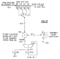
- the timing recovery block 62 accepts inputs I tr and Q tr and outputs a digital error signal representative of the difference between the transmitted signal rate and the rate used to initially sample the incoming signal. It also outputs a lock detect signal 1130 to a lock detect circuit 1064, the operation of which will be described in further detail below.
- the digital error signal is converted to an analog signal by digital to analog converter 1060.
- the analog signal is passed to a voltage controlled crystal oscillator 1062 which controls the frequency at which the signal is sampled in the analog-to-digital converter 60.
- the inphase and quadrature signal components I tr and Q tr are first attenuated by amplifiers 1106 and 1108 which each amplify the signal components with gain of 1/256.
- the delay feedback loops 1102 and 1104 each amplify the attenuated signal components with gain of 255/256 and delay the signal components as indicated by one cycle. This operation causes the timing recovery to be primarily dependent on the signal's past history while also remaining somewhat dependent on the present state of the signal, thereby providing low pass-filtered versions of the inphase and quadrature signal components I tr and Q tr .
- a fewer bit input digital-to-analog converter can be operated simply by connecting the higher order bits to the digital-to-analog converter and not using the least significant bits of the output of the sigma-delta modulator.
- the lowest order bits not output to the digital-to-analog converter can be used in the feedback loop of the sigma-delta modulator 1216.
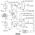
- the proportional integral loop filter 1226 operates in a second mode to make finer adjustments to the tuning frequency.
- the second (fine) adjustment mode constant coefficients I 2 or P 2 are used as inputs to the multipliers.
- the sign of the signal component is not passed by AND gate 1222, and is not used in that mode.
- Sigma-delta modulator 1216 receives fifteen bit input SDIN(14:0) from frequency and phase locked loop 1214, and outputs a ten bit wide signal to digital-to-analog converter 1206.
- adder 1254 produces a 16-bit wide output.
- the 16-bit output is fed into a limiter 1262 which saturates when the 16 bit number exceeds 14 bit number capability, outputting the limited 14 bit number.
- the resultant 14-bit stream [13:0] is then divided into two parts: the ten most significant bits are fed directly into the digital-to-analog converter 1206, while the four least significant bits are fed back to the adder 1254 through delay unit 1266.
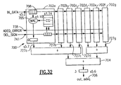
- a block of interleaved derandomized data is read into an internal RAM buffer, elements of which are shown generally at 300. It is an aspect of the invention that only one 3328 byte RAM is required for the deinterleaver, because, as explained in further detail below, as data is being output from the RAM 300, new data from the succeeding interleave block is being written to the same location.
- This approach nearly minimizes the amount of on-chip RAM required at the expense of a slightly more complicated addressing scheme. Further reduction of RAM could only be attained at the expense of significantly increasing the complexity of the control structure with very little gain.
- the timing generator is a simple eight cycle gray code counter. Its primary outputs, indicated in Fig. 17, are decoded to control the RAM timing strobes.
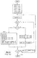
- Control of the read-write-modify operation in the RAM 300 is explained with reference to the following fragment of C code: Initially the RAM 300 is empty, and state is filling. During filling the buffer is consuming incoming data but not producing any output. When the first block has been read in, addr has reached the value 3227, and a full strobe line (not shown) is asserted. State is the changed to ru nning. Here data from a succeeding block is concurrently consumed while deinterleaved data is output from the RAM 300. The running state persists until a channel change occurs, at which point the RAM 300 is allowed to read out until the end of the current interleaved block. State is changed to emptying and data is output until the end of the interleaved block. No further data is consumed during the emptying state.
- agc_value agc_value+ (((abs (data) - bias) >> gain) + 1) >> 1 where bias is either agc_av_bias 618 or agc_train_bias 620, as selected by the mode signal 602 in multiplexer 616, and gain is either agc_av_gain 604 or agc_train_gain 606, depending on the mode.
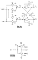
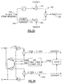
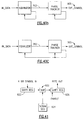
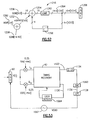
- a matched filter 63 is placed in the path of the received signal after the analog-to-digital converter 60.
- the filter 63 is known as a matched filter because its response matches the response of a similar filter in the transmitter and therefore maximizes the signal-to-noise (SNR) ratio for the bandwidth available.
- the preferred transmitting system includes a filter 63 which shapes the received signal pulses so that their amplitude versus time characteristic is optimum for the channel over which the pulses travel.
- the shape which has been found to be optimum for transmission is that of a raised cosine pulse.
- the application of such pulse-shaping enables each cycle of the periodic waveform to carry two pulses.
- a filter having identical characteristics i.e. a "matched filter” must be provided in the receiving system.
- both the transmitter and receiver have such matched filters, the combination of the shaping performed by the filters of both the transmitter and the receiver must be equal to a raised cosine pulse.
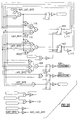
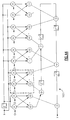
- Figs. 45-46 The resulting tap structures are shown in Figs. 45-46, where the sign inputs to the exclusive-or gates 1034, 1036, 1044, 1046, and the select lines of the multiplexers, 1033, 1035, 1043, 1045 are controlled according to a combination of the signs of the data, the real and imaginary coefficients, and the current position of the down-conversion sequence.
- the logic 742 which performs the adaptation is docked 4 times each symbol period and is thus shared among the data clocked through shift register 708.
- a delayed version of the sign 741 is used to control an adder or subtracter 736 which increments or decrements a coefficient register value in registers 720-723 by the value of the error adeq_error 738.
- the delayed sign 741 is there to model the delay between the multiplication of the data in multiplier 716, and tot allow for the time required for the data to flow through the system and generate an error value. It is important that the sign used is the sign that was in the tap when the error was generated, or which caused the error to be generated.
- a delayed sign shift register 740 operates in parallel with the main data register 708, and is switched by switch 734, which operates similarly to switch 714. The same process is performed on all the taps.
- the phase tracker 754 adapts the value of ⁇ using an error signal also derived from the LMS algorithm, as shown in Figs. 34, 35 and 37.
- the Hilbert filter is an eleven tap finite impulse response filter which has been implemented in much the same way as the finite impulse response filter 750, except that the coefficient values are hardwired.
- One cell is referenced generally at 782. Again, to reduce hardware, the multiplier 786 is shared.
- Fig. 14 differs from the algorithm in Fig. 13. Instead of exchanging the contents of register R2 232 with register R3 233, and exchanging register R4 234 with register R5 235, a toggle switch is used to remember which register contains the respective polynomial. This approach is economical, as temporary storage is not required.
- Resynchronization is necessary in order to correctly transfer data from the Reed Solomon decoder at the 7.5 MHz symbol rate clock into the external processing environment which may operate at a different clock rate. Buffering is necessary because the data is received from the channel at a relatively slow speed in relation to the transfer speed required by the external processing environment. Handshaking control is necessary to ensure that the data is properly transferred from the receiving system of the present invention to the external processing system.
- the output interface first assembles bytes together into 32-bit words. With reference to Fig. 55, bytes arrive one at a time from the Reed Solomon decoder 72 (Fig.
- the potential propagation of an indeterminate signal condition is avoided in the output interface according to the present invention by gating the outgoing control signal DATA_VALID 1308 from the receiving system's internally clocked control element, control 1306, through a series of latches 1310, 1312 and 1314 which are all clocked by the external processing environment's clock 1316. After passing through the series of latches 1310, 1312, and 1314, the likelihood that the signal emerging from the final latch 1314 will remain in an indeterminate condition becomes vanishingly low. Once the signal DATA_VALID 1308 is fully propagated through latches 1310, 1312 and 1314, it is input into another control element 1318.
Abstract
Apparatus for processing a train of signal pulses having even-numbered and odd-numbered
pulses, comprising :
This apparatus further comprises :
a plurality of adding circuits, each connected to an output of a said first multiplier and an output of a said second multiplier.

Description
This invention relates to processing signals received from a communications channel. More particularly this invention
relates to an integrated signal processing system for receiving signals suitable for use in the transmission of video,
"hi-fi" audio, images or other high bit rate signals.
Encoded transmission of inherently analog signals is increasingly practiced today as a result of advances in signal
processing techniques that have increased the bit rate achievable in a channel. At the same time new data compression
techniques have tended to reduce the bandwidth required to acceptably represent analog information. The art is presently
striving to more efficiently transmit video and audio data in applications such as cable television using digital techniques.
Various modulation techniques have been employed in digital communications. For example quadrature amplitude
modulation (QAM) is a relatively sophisticated technique favored by practitioners of digital radio communications. This
method involves two separate symbol streams, each stream modulating one of two carriers in quadrature. This system
achieves spectral efficiencies, between 5 - 7 bits/sec-Hz in multilevel formats such as 64-QAM and 256-QAM. QAM is
particularly useful in applications having a low signal-to-noise ratio. However double sideband modulation is required.
Furthermore cross-coupled channel equalizers are generally needed, which adds to the overall complexity of the system.
A variant of QAM is quadrature phase shift keying (QPSK), in which a signal constellation consisting of four symbols
is transmitted, each having a different phase and a constant amplitude. The scheme is implemented as the sum of
orthogonal components, represented by the equation.
Am = bej m
where m can be any of {0, π/2, π, 3π/2}. It is necessary to transmit both sidebands in order to preserve the quadrature
information.
Another modulation scheme known to the art is vestigial sideband (VSB) modulation, which is achieved by amplitude
modulating a pulsed baseband signal, and suppressing a redundant sideband of the amplitude modulated (AM)
signal, in order to conserve bandwidth. Usually the lower sideband is suppressed. In the digital form of VSB, a digital
pulse amplitude modulated (PAM) signal is employed.
It is proposed in Citta et al., Practical Implementation of a 43 mbit/Sec (8 bit/Hz) Digital Modem for Cable Television,
1993 NCTA Technical Papers, pp 271 - 278, to implement a 16 level VSB modulation method in cable television applications,
wherein symbols of 16 discrete methods are amplitude modulated, using carrier suppression and transmission
of a vestigial sideband in a 6 MHz channel. Transmission of a low level pilot carrier, located approximately 310 kHz
above the lower channel edge, is included to assist in signal detection. The arrangement provides for the transmission
of 43 Mbit/sec, but requires a passband of 5.38 MHZ at 4 bits/symbol.
Reference is made to the detailed description of the invention which is to be read in conjunction with the following
drawings, by way of example wherein:
It is a primary object of the present invention to provide an improved system for the communication of digital data
in a constrained channel.
It is another object of the invention to provide an improved, economical apparatus for receiving and decoding data
at high bit rates, such as video and audio signals.
It is yet another object of the invention to provide an improved, highly accurate analog-to-digital converter which can
operate at high speeds and is suitable for the processing of video signals.
It is still another object of the invention to provide an improved compact filter that can reduce a modulated signal to
a complex baseband representation and concurrently perform a Nyquist operation.
It is a further object of the invention to provide an improved and highly compact deinterleaving circuit that can be
economically implemented in a semiconductor integrated circuit.
It is another object of the invention to provide an output interface for a digital receiver that synchronizes the data
flow through the receiver with a transmission rate of the signal.
These and other objects of the present invention are attained by a passband pulse amplitude modulation (PAM)
receiver employing multilevel vestigial sideband modulation. A particular form of the invention is suitable for transmitting
MPEG 2 transport layer data. MPEG is a standard well known to the art, in which data is grouped in a plurality of packets,
each of which contains 188 bytes. This number was chosen for compatibility with asynchronous transfer mode
(ATM) transmissions, another known telecommunication standard. The apparatus disclosed herein relies on randomization
of the data prior to transmission, using a signal constellation having a zero mean.
The invention provides a signal processing apparatus for the reception of data packets that are transmitted through
a channel, wherein the data packets include information data and error correction data for correcting errors in the
received data, and the packets are represented in a modulated signal having pretransmission characteristics, and are
demodulated following transmission. The signal processing apparatus comprises an analog-to-digital converter for
sampling an input signal following transmission of the input signal through a communications channel. A timing recovery
circuit is coupled to the analog-to-digital converter output for adjusting the frequency and the phase of the sampling
intervals. A carrier recovery circuit is coupled to the analog-to-digital converter output for adjusting the frequency and
phase of the input signal. An automatic gain control circuit is also coupled to the analog-to-digital converter output, and
provides an error signal that is indicative of a magnitude of the input signal and a reference magnitude. A filter conforms
the analog-to-digital converter output to pretransmission characteristics of the input signal. An adaptive equalizer is
coupled to the filter, and has characteristics that are adaptively varied in accordance with predetermined information
encoded in the modulated signal, so that the equalizer output compensates for channel characteristics. An error correcting
circuit is coupled to the equalizer and to an output interace. The timing recovery circuit, the carrier recovery circuit,
the equalizer, the error correcting circuit, and the output interface are integrated on a semiconductor integrated
circuit.
In an aspect of the invention the modulated signal is modulated by vestigial sideband modulation, and there is provided
an amplifier coupled to the channel and accepting the modulated signal therefrom, and a demodulator coupled
to the amplifier for producing a demodulated signal.
In another aspect of the invention a plurality of the data packets are grouped in frames, each frame further comprising
a frame header, while the predetermined information comprises a training sequence in the frame header.
In another aspect of the invention the equalizer comprises a first response filter, and a circuit for adjusting coefficients
of the first response filter that is responsive to an error signal that is derived from a difference between an output
of the first response filter and the predetermined information. The circuit for adjusting the coefficients executes the
signed least-mean-square algorithm.
The equalizer also includes a phase tracking circuit for producing an in-phase component and a quadrature component
that is representative of the modulated signal in accordance with the formula
data = a (t )cos+ â (t )sin
wherein
In another aspect of the invention the first and second response filters are finite impulse response filters, and the
second response filter performs a Hilbert transform.
In another aspect of the invention blocks of the packets are interleaved at an interleaving depth, and a deinterleaving
circuit is incorporated in the integrated circuit. The deinterleaving circuit comprises a random access memory for
memorizing the interleaved packets, which has a capacity that does not exceed a block of interleaved data, and is
organized in a plurality of rows and a plurality of columns, wherein the rows define a plurality of groups. A first circuit
generates an address signal representing a sequence of addresses of the random access memory, wherein successive
addresses differ by a stride. A second circuit successively reads and writes data out of and into the random access
memory respectively at an address of the random access memory that is determined by the address signal. A third circuit
increases the stride by the interleaving depth, wherein the stride is increased upon deinterleaving of a block of interleaved
data.
In another aspect of the invention the deinterleaving circuit further comprises a control circuit for operating the second
circuit in a selected one of a first operating mode, wherein the random access memory is accepting incoming data
and is not producing outgoing data; a second operating mode, wherein the random access memory is accepting incoming
data and producing outgoing data; and a third operating mode, wherein the random access memory is not accepting
incoming data and is producing outgoing data. The first circuit comprises a predecoder that preselects one of the
groups of rows in the random access memory, and a row decoder that selects a row of the preselected group.
An input of the analog-to-digital converter has a modulated input that exceeds baseband, and the filter has a plurality
of coefficients that are arranged to reduce the output of the analog-to-digital converter to a complex baseband representation
of the modulated signal.
In an aspect of the invention the integrated circuit is a CMOS integrated circuit.
In another aspect of the invention the filter is integrated in the integrated circuit.
In another aspect of the invention the analog-to-digital converter is integrated in the integrated circuit.
In another aspect of the invention the automatic gain control circuit is integrated in the integrated circuit.
In another aspect of the invention the analog-to-digital converter comprises a comparator having first and second
units, each of the units comprising a capacitor connected to a first node and a second node. A first switch means connects
the first node to a selected one of an input voltage and a reference voltage. An inverter is connected to the second
node and has an output, and the inverter has a small signal gain between the second node and the output thereof. A
second switch means connects the output of the inverter of one of the first and second units to the first node of another
of the first and second units, whereby the first and second units are cross-coupled in a positive feed back loop when the
second switch means of the first unit and the second switch means of the second units are closed. The output of the
inverter is representative of a comparison of the input voltage and the reference voltage. Each unit further comprises a
third switch means for connecting the first node and the output of the inverter, whereby an input of the inverter is zeroed.
In another aspect of the invention the inverter, the first switch means, the second switch means, and the third switch
means comprise MOS transistors.
In another aspect of the invention the filter down converts the input signal to complex baseband representation and
performs a Nyquist operation on the input signal.
In another aspect of the invention the error correcting circuit comprises a Reed-Solomon decoder, which comprises
a circuit for executing a Berlekamp algorithm. The circuit comprises a first register for holding a portion of a locator polynomial
Λ(x), a second register for holding a portion of a D polynomial, a first switch means for alternately selecting the
first register and the second register in successive iterations of the Berlekamp algorithm. The circuit further comprises
a third register for holding a portion of an evaluator polynomial Ω(x), a fourth register for holding a portion of an A polynomial,
and a second switch means for alternately selecting the third register and the fourth register in successive iterations
of the Berlekamp algorithm.
The invention provides a method of signal processing received data packets that are transmitted through a channel,
wherein the data packets include information data and error correction data for correcting errors in the received data,
and the packets are represented in a modulated signal having pretransmission characteristics, and are demodulated
following transmission, comprising the steps of sampling an input signal at sampling intervals following transmission of
the input signal through a channel. While the step of sampling is being performed, a frequency and a phase of the sampling
intervals and a frequency and a phase of the input signal are adjusted. An error signal is provided that represents
a difference between the signal that is indicative of a magnitude of the input signal and a reference magnitude. The
sampled input signal is filtered to conform a post-sampling characteristic thereof to a pretransmission characteristic
thereof. The filtered input signal is adaptively equalized in accordance with predetermined information encoded in the
modulated signal in order to conform the filtered input signal to characteristics of the channel. The adaptively equalized
input signal is submitted to an error correcting circuit to produce corrected data, and the corrected data is output. The
step of adjusting a frequency and a phase of the input signal, the step of providing an error signal, the step of filtering
the sampled input signal, the step of adaptively equalizing the filtered input signal, and the step of submitting the adaptively
equalized input signal to an error correcting circuit are performed using a semiconductor integrated circuit.
The invention provides a filter for operating upon a sampled signal comprising an arrangement of adders, multipliers,
and multiplexers having a pulse-shaping response, in which the multipliers are arranged to multiply factors corresponding
to samples of the signal by constant coefficients, the constant coefficients are selected for use in
simultaneously shifting the signal in frequency and shaping pulses of the sampled signal according to the pulse-shaping
response.
In one aspect of the invention the pulse-shaping response is a square-root raised cosine response.
In an aspect of the invention the pulse-shaping response is a square-root raised cosing response.
The invention provides a filter for operating upon a signal sampled at a rate exceeding the minimum Nyquist sampling
frequency, which has an arrangement of multipliers, adders, and multiplexers arranged to operate upon a first portion
of samples of the sampled signal while discarding a second portion of the samples, thereby preserving information
transmitted within the bandwidth of the sampled signal, while reducing the number and frequency of the samples to be
propagated.
In an aspect of the invention the first portion of the samples corresponds to symbol pulses.
In another aspect of the invention the first portion of the samples corresponds to one symbol per sample.
The invention provides an output interface for transferring data from a data source operating at a first clock rate provided
by a first clock signal to a data sink operating at a second clock rate provided by a second clock signal. The interface
has a first latch operable at the first clock rate, a second latch operable at the second clock rate. The second latch
receives data from the first latch. The interface includes a first signal generator operable at the first clock rate, producing
a data valid signal, and includes at least one third latch operable at the second clock rate. The third latch receives the
data valid signal from the first signal generator in response to the second clock signal. A second signal generator is
operable at the second clock rate, and activates a load data signal to the second latch in response to receipt of the data
valid signal from the third latch. Data is thereby transferred from the first latch to the second latch in response to receipt
by the second latch of the second clock signal when the load data signal is active.
The invention provides an output data error signaling system for signaling the presence or absence of an error in
at least one multiple byte packet to an external processing environment. The multiple byte packet includes at least one
error indicator, and has a buffer, the buffer storing at least one multiple byte packet. There is provided a packet error
indicator, signaling an error condition of the packet to the external processing environment after receipt by the buffer of
at least a portion of a packet containing an active error indicator bit.
As used herein the notation sK.N indicates signed 2's complement integers having a magnitude varying from 0 to
2K-1, and N bits of fraction. An unsigned integer is represented as K.N.
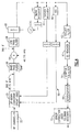
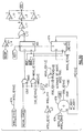
Turning now to the Drawing, and to Fig. 1 thereof, a communication system that is embodied by a preferred embodiment
of the invention is generally referenced 10. A data source 12, such as a television signal, is submitted to a source
encoder 14 to yield a bit stream that is processed through a channel encoder 16. It will be understood by those skilled
in the art that the source encoder 14 is arranged to minimize the bit rate required to represent the data with a desired
fidelity, and that the channel encoder 16 maximizes the information rate conveyed through a channel with less than a
predetermined bit error probability. The arrangement of the data is discussed for convenience with reference to the
MPEG2 (ISO/IEC JTC1/SC29/WG11N0702) digital transmission scheme, it being understood that many other kinds of
data, grouped in packets of various sizes can be transmitted within the scope and spirit of the invention. In the preferred
embodiment the transport stream from the data source 12 is formed by the source encoder 14 into 188 byte groups, in
conformance with the MPEG 2 standard, and a Reed Solomon code is applied by the channel encoder 16, wherein
each 188 byte group has 20 appended check bytes to form a 208 byte packet. Reed Solomon codes are known to provide
high coding gains, and with this arrangement it is possible to correct up to 10 byte errors per packet. The details of
the Reed-Solomon (208, 188) code are as follows:
Galois Field (256) arithmetic is used. The field generator polynomial is given by x8 + x4 + x3 + x2 + 1. A primitive
element, αx, is the xth member of the Galois Field, and the code generator polynomial is given by:
i =0 19 (x + ai )
The following C program correctly generates the Reed Solomon code.


The bytes in the Reed-Solomon encoded packets are then subjected to 16-way interleaving in order to better tolerate
burst errors that could exceed the correction capabilities of the Reed-Solomon technique. This is accomplished, as
indicated in Table 1, by writing byte packets rowwise into a 208 x 16 byte array, and reading the data by columns.
| Interleave Structure | |||||
| 0 | 1 | 2 | ... | 206 | 207 |
| 208 | 209 | 210 | ... | 414 | 415 |
| ... | ... | ... | ... | ... | ... |
| 3120 | 3121 | 3122 | ... | 332 6 | 3327 |
The 3328 bytes are written in the order 0, 1, 2,...,3327, and read in the order 0, 208, 416,...,3120, 1,209, ..., 3121,
... With this arrangement up to 42 microseconds of burst errors can be tolerated, assuming the a transmission rate of
30 megabits/second using 16-VSB.
The resultant interleaved block is passed through a transmit filter 18 and a modulator 20, as shown in Fig. 1. The
digital communication scheme discussed herein assumes that randomized data is being transmitted with zero mean1 to
keep from transmitting with direct current (DC) bias. To achieve randomization, the data is subjected to a bit-wise exclusive
OR operation with a pseudorandom sequence generated by a feedback shift register. The random number generator
employs an 11 bit shift register (not shown) which is initialized to 1s. The generator function is the polynomial
1 + x9 + x11.
Groups of interleaved blocks of data thus formed are transmitted along with a periodic frame header, which contains
a frame synchronization sequence and a training sequence. The purpose of the latter will be explained in further
detail below.
The frame structure is shown in table 2. The frame header includes a 31 symbol frame sync, 775 symbol training
sequence, and a 26 symbol user data field.
| Frame Header | Data | |
| 16-VSB | 832 symbols | 320 packets (20 interleaved blocks) |
| 8-VSB | 832 symbols | 240 packets (15 interleaved blocks) |
| 4-VSB | 832 symbols | 160 packets (10 interleaved blocks) |
| 2-VSB | 832 symbols | 80 packets (5 interleaved blocks) |
The generator polynomial for the frame sync is x5 + x4 + x2 + x + 1 , with an initial condition of 00001 (binary).
This yields the frame sync sequence:
sseq = 1,0,0,0,0,1,1,1,0,0,1,1,0,1,1,1,1,1,0,1,0,0,0,10,0,1,0,1,0,1.
sseq = 1,0,0,0,0,1,1,1,0,0,1,1,0,1,1,1,1,1,0,1,0,0,0,10,0,1,0,1,0,1.
The generator polynomial for the training sequence is x5 + x3 + 1 , with initial condition 00100 (binary). This yields
the training sequence:
tseq = 0,0,1,0,0,0,0,1,0,1,0,1,1,1,0,1,1,0,0,0,1,1,1,1,1,0,0,1,1,0,1.
tseq = 0,0,1,0,0,0,0,1,0,1,0,1,1,1,0,1,1,0,0,0,1,1,1,1,1,0,0,1,1,0,1.
The complete frame header consists of:
sseq + 12 x (tseq' + tseq) + tseq' + userdata[0..25], where tseq' is identical to tseq, except that the last bit is inverted from 1 to 0.
sseq + 12 x (tseq' + tseq) + tseq' + userdata[0..25], where tseq' is identical to tseq, except that the last bit is inverted from 1 to 0.
The user data field contains two sets of two bits which each specify the modulation level (16-VSB, 8-VSB, 4-VSB
or 2-VSB), two bytes of user data and a 6 bit cyclic redundancy check (CRC) field as shown in table 3.
The modulation level is defined in table 4.
| User Data Field | ||||
| VSB Levels | VSB levels | user_reg() | user_reg1 | CRC |
| 2 bits | 2 bits | 8 bits | 8 bits | 6 bits |
| VSB Modulation Level Field | |
| vsb-levels [1:0] | VSB modulation |
| 0 | 16-VSB |
| 11 | 8 VSB |
| 10 | 4 VSB |
| 01 | 2 VSB |
The CRC is generated as follows: the sequence "vsb_levels[1:0], vsb_levels[1:0], user_reg0[7:0],
user_reg[7:0],0,0,0,0,0,0" forms the dividend of a CRC with generator polynomial G(x) = x6 + x5 +x4 +1. The remainder
is CRC[5:0]. A generator of a user data CRC generator is shown in Fig. 22.
The sequence "vsb_levels[1:0], vsb_levels[1:0], user_reg0[7:0], user_reg[7:0], CRC[5:0]" is scrambled by exclusive
ORing with the first 26 bits of the training sequence tseq.
Data is transmitted as symbols consisting of 4 bits for 16-VSB, 3 bits for 8-VSB, 2 bits for 4-VSB, or 1 bit for 2-VSB.
Bytes from the interleaver must be converted to symbols MSB first. Mapping to 16-VSB is explained with reference to
Fig. 2. A bitstream 34 is formed of three bytes 36a, 36b, 36c, which are also represented vertically in the central portion
of Fig. 2, with the MSB at the top. Each of the three bytes 36a-c is broken into two symbols 38 - 43. Symbols 38 and 39
contain the 4 most significant and least significant bits respectively of byte 36a. The contents of symbols 40 - 43 relate
to bytes 36b-c in like manner.
Fig. 3 explains the mapping from bytes to symbols for 8-VSB. Here the bits of the three bytes 26A-C are arranged
in groups of three bits, with crossing of byte boundaries, for example at symbol 44c of the three groups 46a, 46b and
46c. Symbols for 4-VSB and 2-VSB are formed in equivalent manners.
The symbol constellations are shown in table 5. The frame header constellation, including the user data, is -8 (logical
0), and +8 (logical 1) for all modulation levels.
| Symbol | Constellation | |||
| 16-VSB | 8-VSB | 4-VSB | 2-VSB | |
| 0x8 | -15 | |||
| 0x9 | -13 | |||
| 0xa | -11 | |||
| 0xb | -9 | |||
| 0xc | -7 | |||
| 0xd | -5 | |||
| 0xe | -3 | |||
| 0xf | -1 | |||
| 0x0 | +1 | +2 | +4 | +8 |
| 0x1 | +3 | +6 | +12 | -8 |
| 0x2 | +5 | +10 | -12 | |
| 0x3 | +7 | +14 | -4 | |
| 0x4 | +9 | -14 | ||
| 0x5 | +11 | -10 | ||
| 0x6 | +13 | -6 | ||
| 0x7 | +15 | -2 |
The transmit filter 18 (Fig. 1) is a square root raised cosine filter having a rolloff of 20%.
Structural details of the source encoder 14, channel encoder 16, transmit filter 18, and modulator 20 are outside
the scope of the invention and will not be further discussed.
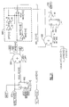
Channel 22 can be any channel, such as a fiber optic link, coaxial cable, microwave, satellite, etc. which is suitable
for the transmission at television, video, "hi-fi" audio or other high bit rate signals. The digital receiver, which will be
described in greater detail hereinbelow, comprises a first demodulator 24, the output of which is filtered through a band
pass filter 21. A second demodulator 27 converts its input to base band. The output of the second demodulator 27 is
passed through a receive filter 28. The signal then passes successively to a channel decoder 30, a source decoder 32,
and finally into a data sink 35. The channel decoder 30 and the source decoder 32 reverse the encoding that was
accomplished in the source encoder 14 and the channel encoder 16 respectively.
The organization of a digital receiver 50 is shown in greater detail in Fig. 4. In the receiver front end 23, shown in
yet greater detail in Fig. 4a, a radio frequency amplifier 52 is coupled to the channel 22 via a high pass filter 51. The
output of the radio frequency amplifier 52 passes through radio frequency attenuater 53 and low pass filter 54 and is
down converted to a first intermediate frequency by the first demodulator 24, and then passed through a low pass filter
25. The first demodulator 24 is of a known type. Its frequency is controlled by a voltage-controlled oscillator 33, programmed
through a microprocessor interface operating through a digital-to-analog converter 37. The second demodulator
27 converts the signal to a second intermediate frequency, and is followed by a high pass filter 29, and another
amplifier stage 31. The output of amplifier stage 31 is passed through a bandpass filter 21 to a third down converter 19
(Fig. 1), which converts the signal to a third intermediate frequency and then passes the signal to a low pass filter 58.
A high speed analog to digital converter 60, provides an output which is used by timing recovery circuit 62, which
ensures accurate sampling by analog-to-digital converter 60. Fig. 23 shows a graph of the signal spectrum at the input
of the analog-to-digital converter 60, wherein frequencies and bandwidth values are shown in MHz. This spectrum
shape can be achieved if the passband of band pass filter 21 is 4.75 MHz below the carrier to plus 0.75 MHZ above the
carrier and there exists a transition band from carrier +0.75 MHz to carrier + 1.25 MHz. The rolloff at the Data Nyquist
frequency (1.875 MHz) is controlled by the bandpass pulse shaping by the transmit filter 18, discussed above. A filter
63 receives the output of the analog-to-digital converter 60, and converts the signal to complex base band representation.
The output of the filter 63 is substantially real. DC bias in the signal is removed in DC Remover block 67.
A carrier recovery circuit 64 controls the second demodulator 27 (Fig. 4a) such that the correct frequency and
phase are recovered. An automatic gain control circuit 66 feeds back to radio frequency attenuater 53 through digital-to-analog
converter 55. Both the automatic gain control circuit 66 and the carrier recovery circuitry 64 are coupled to
the output of analog-to-digital converter 60. An adaptive equalizer 70 contends with various channel impairments such
as echoes and multipath transmission.
The main digital data stream from the analog-to-digital converter 60 is filtered by a matched filter, which matches
the response of the transmit filter 18. The digital stream is also derandomized and deinterleaved in deinterleaver 69.
The equalized signal is then subjected to Reed-Solomon decoding and error correction in error correction circuitry 72.
Except for the front end 23, the receiver 50 is largely realized as an integrated CMOS device by well known methods.
There are many applications which require a fast and accurate comparator, and achieving the design in CMOS
makes integrating such applications an inexpensive alternative to using external support. An example of an application
is the flash analog to digital converter (denoted FADC), where a linear array of comparators convert an analog voltage
into a digital representation.
CMOS comparators have a poor gain characteristic, which eventually limits the speed of comparison, and the input
referred offsets are large, limiting the resolution of the comparison.
Another set of problems are switching noise through the supplies and substrate from unrelated blocks of circuitry,
and switch noise from sampling devices. These problems are usually solved by using a balanced differential system.
Most amplification systems are characterized by a time constant, τ, and a gain G. The evolution of the output of a
comparator is generally given by the form
Vout = G (Vin -Vref )(1-et/τ )
Obviously, after a time t, the output is determined solely by G and τ. For CMOS, to make G large enough necessarily
makes τ larger, and so a small input (Vin-Vref) will take a long time to reach a clearly delimited logic level. This limits the
speed of comparison, particularly when the design requires accuracy, that is a small (Vin-Vref) to resolve.
The best performance in CMOS comes from using positive feedback. This gives a large gain G with a small τ as
desired. The drawbacks are
The input referred offsets are mainly due to the mismatch of the transistors used to implement the comparator. All
the transistor mismatch can be modeled as a mismatch in a single parameter, usually the threshold voltage, Vt. The
equation for the current in a MOS transistor is given by
I = β WL V ds (V gs -V t -Vds 2 )
where
- β
- is a physical gain term;
- W/L
- is the width/length ratio of the transistor;
- Vds
- is the voltage from the Drain to the Source;
- Vgs
- is the voltage from the Gate to the Source; and
- Vt
- is the threshold voltage, which is a physical characteristic.
Even if two transistors are adjacent, well-matched, on the same substrate and are biased identically, the current
which flows is different because the Vt is not controlled. A difference of +/- 40mV in a term of approximately 700mV is
common, particularly if standard available CMOS process is used.
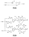
The input referred offset is shown in Fig. 5a, which illustrates a comparator 77. The input referred offset, Vo 78,
appears in series with the input Vin, and affects directly the comparison of Vin and the reference voltage Vref. The comparison
operation performs
Vin + Vo - Vref
and gives a result of a logic ONE if this sum is positive, and a logic ZERO otherwise. The offset Vo 78 can be positive
or negative, since the mismatch can go either way, and so for a ONE it must be guaranteed that Vin > Vref + |Vo | , and
for a logic ZERO it must be guaranteed that Vin < Vref - |Vo | . The offset voltage Vo 78 therefore appears as a window
of magnitude Vo, centered around Vref, in which the output of the comparison is not guaranteed to be correct.
By way of example, a 1V peak-to-peak input into an 8-bit FADC, requires the comparator to successfully resolve a
difference of at least one LSB. Since the FADC resolves to 8-bit precision there are 28 or 256 levels. Therefore, the
FADC must be capable of resolving to 1V / 256 = 3.9 mv. In general, existing systems require a resolution capability of
one half the voltage differential of an LSB. With the example Vt mismatch of 40mV between two adjacent devices and
the use of a two-transistor input stage this comparison is not achievable, since the comparator will not correctly resolve
a difference of less than 40mV.
The usual solution is to use a system which zeros the offset voltage Vo. The two main techniques used are:
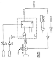
The comparator of the present invention is shown schematically in Fig. 5b. The implementation of inverters 76 and
79 is not important, although it is assumed that the inverters 76, 79 have some small signal gain, g, greater than one.
The operation of the comparator will be described in three phases. In phase 1, switches 80, 81, 82, and 83 are
closed; the other switches in Fig. 5b are open. Switch 80 drives the node X to the voltage Vin. Switch 81 drives the node
X to the voltage Vref. Switch 82 connects inverter 76 with negative feedback ensuring that the input voltage and the output
voltage are the same. This voltage is Vth, the threshold voltage of the inverter 76, and does not depend on any input
offset. The net effect is to zero the input to the inverter 76. Switch 83 zeroes inverter 79. It should be noted that the voltages
on Y and Y are not necessarily the same.
In phase 2, switches 84 and 85 are closed, the others open. Since nodes Y and Y are not driven, some fraction
(near one) of the voltage change on X and X respectively will accrue due to the action of capacitors 86 and 87. Switch
84 drives the voltage Vref onto node X, thus causing a voltage change of (Vin - Vref). The voltage accrued on Y will be
some fraction of (Vin - Vref), say f1(Vin - Vref), where f1 is approximately 1.0. Switch 85 drives the voltage Vin onto node
X thus causing a voltage change of Vref - Vin. The voltage accrued on Y will be some fraction of (Vref - Vin). say f2 (Vref
- Vin), where f2 is approximately 1.0.
The small signal gain of an inverter is given by:
Vout - Vth = g(Vin - Vth )
and so the voltage on node Q will reach a value V given by:
V-V1 = g1(f1(Vin -Vref )-V1)
where V1 is the zero voltage for inverter 76; and the voltage on node Q will reach a value V given by:
V - V2 = g2(f2.(Vref - Vin ) - V2)
where V2 is the zero voltage for inverter 79.
In phase 3, switches 88 and 89 are closed, and switches 80, 81, 82, 83, 84 and 85 are open. To understand the
operation, it is easier to assume that g1 = g2 = g and f1 = f2 = f and V1 = V2 = Vth . This is approximately correct, and
is mathematically more clear. Switches 88 and 89 connect inverters 76 and 79 in positive feedback. The input voltage
applied before feedback starts is just (V - V ).
V - V = g f(Vin - Vref - (Vref -Vin )) = 2gf(Vin - Vref )
Assuming the f is approximately 1.0, an amplifier is now connected in positive feedback with an input magnitude of
2g(Vin - Vref). The original signal has been amplified by a factor of 2g before positive feedback is applied.
The system including inverters 76, 79 connected with positive feedback has an input referred offset, but if the
designer ensures that 2g is large enough, then the comparison can be guaranteed.
The circuit of Fig. 5b is fully symmetric, balanced and differential. Any common-mode switching noise will be
rejected. Control of the switches according to phases 1 - 3 may be accomplished, for example by a 3:1 counter, or a 3
stage shift register.
Fig. 6a is a CMOS circuit corresponding to the circuit of Fig. 5b, which is preferably used with transistors 90-97
replacing switches 80, 84, 81, 85, 82, 83, 88, 89 and the inverters 76, 79 implemented as shown in Fig. 6b, wherein
inverter 98 is comprised of a PMOS transistor 99 and an NMOS transistor 100. The CMOS circuit of Fig. 6a is preferably
included in the integrated circuit of the receiver 50. In Fig. 6a, switch control values of P1 - P3 are as follows:
| P1 = HIGH | PHASE 1 | P2=P3=LOW |
| P2 = HIGH | PHASE 2 | P1=P3=LOW |
| P3 = HIGH | PHASE 3 | P1=P2=LOW |
In order to properly detect the received data from the sampled signal emerging from the analog-to-digital converter
60 (Fig. 4), it is necessary to accurately follow the timing of the received signal. Fig. 53 shows a block diagram of the
portion of the receiver controlling analog-to-digital converter sample timing, and Fig. 54 shows the timing recovery portion
in detail.
As described with reference to Fig. 53 and Fig. 23, samples of the received signal, x(t), emerge from the analog-to-digital
converter as a 15 megasamples per second signal having a carrier frequency at 5.625 MHz and a rolloff at
data Nyquist of 1.875 MHz. The output of analog-to-digital converter 60 is split, and each branch multiplied with a periodic
signal to provide signal inphase (real) and quadrature (imaginary) components Itr and Qtr respectively, which have
been down converted from the third intermediate frequency so that the data Nyquist frequency (1.875 MHz) has been
shifted down to 0 Hz (DC). The timing recovery block 62 accepts inputs Itr and Qtr and outputs a digital error signal representative
of the difference between the transmitted signal rate and the rate used to initially sample the incoming signal.
It also outputs a lock detect signal 1130 to a lock detect circuit 1064, the operation of which will be described in
further detail below. The digital error signal is converted to an analog signal by digital to analog converter 1060. The
analog signal is passed to a voltage controlled crystal oscillator 1062 which controls the frequency at which the signal
is sampled in the analog-to-digital converter 60.
As shown in Fig. 54, inside the timing recovery circuit of the system there are provided delay feedback loops 1102
and 1104. The inphase and quadrature signal components Itr and Qtr are first attenuated by amplifiers 1106 and 1108
which each amplify the signal components with gain of 1/256. The delay feedback loops 1102 and 1104 each amplify
the attenuated signal components with gain of 255/256 and delay the signal components as indicated by one cycle. This
operation causes the timing recovery to be primarily dependent on the signal's past history while also remaining somewhat
dependent on the present state of the signal, thereby providing low pass-filtered versions of the inphase and quadrature
signal components Itr and Qtr.
The resultant components are next multiplied together by multiplier 1110. This produces a signal ItrQtr 1113 which
is proportional to the sine of the frequency difference between the symbol rate and the frequency of the sampling rate
which was used.
The signal ItrQtr 1113 is output directly as a lock detect signal 1130. At the same time, the signal ItrQtr 1113 is
applied to a proportional integral loop filter 1111. In the proportional integral loop filter 1111, the result is applied to two
selective gain amplifiers 1112 and 1114 which can be operated alternately with a non-steady state gain value and with
a steady state gain value. Thus, the gain on the integral side of the proportional integral loop filter 1111 is switched by
selector 1116 to tmr_i_gain_ac during the acquisition phase in "locking" onto the signal timing. Once lock has been
acquired, selector 1116 switches the gain to the steady state value, tmr_i_gain_run. The process occurs in parallel on
the proportional side of the filter, as the amplifier gain is switched by selector 1118 between acquisition gain
tmr_p_gain_ac and steady state gain tmr_p_gain_run.
The signal on the proportional side of the proportional integral loop filter is amplified without integration and passed
forward. The signal on the integral side of the filter, however, is integrated and then passed to an adder 1120 to be combined
with the signal emerging from the proportional gain amplifier. The two signals are recombined by adder 1120 and
output as a 9-bit error signal 1132 which is then sigma-delta modulated in a sigma-delta modulator 1134 to form the
single bit output TCTRL 1136. The output TCTRL 1136 is filtered by low pass filter 1138 and presented to the input of
the voltage-controlled crystal oscillator 1062.
The lock condition is detected from the unprocessed lock detect signal 1130 of the filter in a sequence of operations
as performed by a lock detect circuit 1064 which is implemented as a state machine. The following C code fragment is
illustrative of the operation of the state machine:

Upon detection of the lock condition, the proportional integral loop filter 1111, changes modes from the "acquisition"
state in which "acquisition" gain values tmr_i_gain_ac and tmr_p_gain_ac have been used, to the locked condition
in which the "run" gain values tmr_i_gain_run and tmr_p_gain_run are used. The acquisition condition is better suited
for the broadband case where, for example, the receiver has just been turned on or the channel selector has just been
switched. The lock condition is intended for use when a steady state condition has been achieved, i.e. the signal has
been locked upon, and a finer, narrow band control over the timing recovery has been made possible.
The gain values used in the proportional-integral loop filter should be chosen to provide the required values of the
loop natural frequency ωn and damping factor zeta. (ζ), given the characteristics of the voltage controlled crystal oscillator,
the external analog low pass filter and the input signal magnitude.
The operations of carrier recovery, phase and frequency locking are performed on the discrete time sampling of the
signal output from the analog-to-digital converter. These functions are performed by the carrier recovery block 64
shown in Fig. 4.
The carrier recovery and locking functions are performed with hardware that is similar to that used for the timing
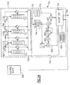
recovery operation. Fig. 48 shows a block diagram of the carrier recovery block, 64 as used in the receiving system of
the present invention. As is evident from Fig. 48, the carrier recovery block 64 receives input in the form of an 8-bit-wide
pulse train at 15 megasamples per second from the analog-to-digital converter 1204 and provides output in the form of
a 10-bit-wide data signal to digital-to-analog converter 1206. The output from digital-to-analog converter 1206 is low
pass filtered through low pass filter 1208, and provides a control signal to voltage controlled oscillator 1210. The voltage
controlled oscillator 1210 in turn is used in the down conversion process of the incoming analog signal as shown in Figs.
4 and 4a.
The blocks used to perform the functions of the carrier recovery block are a down converter 1212, a frequency and
phase locked loop (FPLL) 1214, and a sigma-delta modulator 1216.
Inside the carrier recovery block 64 (Fig. 48) a down conversion from the third intermediate frequency to baseband
is performed. Down conversion is performed in a manner similar to that used by the matched filter, as herein described
below with respect to Figs. 42-46. Successive pulses of the 15 megasamples per second analog-to-digital converter
output signal 1204 are multiplied by complex coefficients representative of a 5.625 MHz periodic function in superheterodyne
manner to convert the signal down to baseband. The resultant baseband inphase and quadrature components
Icr and Qcr are then passed to the frequency and phase locked loop 1214.
Frequency and phase locked loop 1214 operates upon 8-bit in-phase and quadrature signal components Icr and
Qcr to generate a 14-bit wide output signal to sigma-delta modulator 1216 which itself, in turn, outputs a 10-bit wide signal
to digital-to-analog converter 1206 for controlling voltage controlled oscillator 1210. The use of a 10 bit wide digital-to-analog
converter 1206 permits a relatively high degree of precision to be obtained in controlling voltage controlled
oscillator 1210. It is possible that a lower degree of precision will be sufficient, even desirable, for operating the receiver
of the present invention. In such case, a fewer bit input digital-to-analog converter can be operated simply by connecting
the higher order bits to the digital-to-analog converter and not using the least significant bits of the output of the sigma-delta
modulator. Alternatively, the lowest order bits not output to the digital-to-analog converter can be used in the feedback
loop of the sigma-delta modulator 1216.
A block diagram of the frequency and phase locked loop 1214 is shown in Fig. 49. As shown in the figure, the "real"
or inphase component of the signal is applied to infinite-impulse response (IIR) filter 1220, while the imaginary or quadrature
component of the signal is applied directly to the multiplier. Infinite-impulse response filter 1220 is used as a low
pass filter in the path of the real signal components to filter out the double frequency harmonics which remain after the
superheterodyne down-conversion. From the output of infinite-impulse response filter 1220, only the sign information of
the signal remains important. The sign information is then gated by AND gate 1222 to multiplier 1224 to produce a signal
p(t) of value, either "Imag" or "-Imag." The resultant signal p(t) is then applied to a proportional integral loop filter
1226.
The proportional integral loop filter 1226 operates in a manner similar to that described for the proportional integral
loop filter 1111 of the timing recovery block. Proportional integral loop filter 1226 has a proportional side wherein signal
p(t) is multiplied by a coefficient P1 or P2. Proportional integral loop filter 1226 also has an integral side wherein the signal
p(t) is multiplied by a different coefficient I1 or I2 and then integrated by a delay unit plus adder feedback loop. The
sum resulting from the addition of signal parts arriving from the proportional and integral sides of the proportional integral
loop filter 1226 forms the output 1230 which is transferred to the sigma-delta modulator 1216.
The proportional integral loop filter 1226 is constructed to operate in two different modes. In the first mode, the proportional
integral loop filter 1226 is used to lock onto the frequency of the received carrier. In this mode, constant coefficients
I1 and P1 are used to tune the receiver to the close frequency range until frequency lock is detected. In the first
mode the sign 1232 of the real signal component is passed by AND gate 1222 to multiplier 1224.
After lock is detected, the proportional integral loop filter 1226 operates in a second mode to make finer adjustments
to the tuning frequency. In the second (fine) adjustment mode, constant coefficients I2 or P2 are used as inputs
to the multipliers. However, in the second mode, the sign of the signal component is not passed by AND gate 1222, and
is not used in that mode.
In this discrete time signal filtering embodiment, constant coefficients I1, I2, P1, and P2 and discrete time pulse trains
which default on "power-up" to predetermined sequences but which can be altered through manipulation by connected
digital devices. As such, the coefficients have the potential to be altered to adjust for different conditions.
Sigma-delta modulator 1216 receives fifteen bit input SDIN(14:0) from frequency and phase locked loop 1214, and
outputs a ten bit wide signal to digital-to-analog converter 1206. At the head of the sigma-delta modulator 1216, adder
1254 produces a 16-bit wide output. The 16-bit output is fed into a limiter 1262 which saturates when the 16 bit number
exceeds 14 bit number capability, outputting the limited 14 bit number. The resultant 14-bit stream [13:0] is then divided
into two parts: the ten most significant bits are fed directly into the digital-to-analog converter 1206, while the four least
significant bits are fed back to the adder 1254 through delay unit 1266.
In Figs. 49 and 52 another feature of the carrier recovery block of the present invention is shown. Should the proportional
integral loop filter 1226 be unable to lock onto the frequency of the received intermediate frequency signal, an
adder 1260 can be used to add a discrete frequency shift value HOP(3:0) to the five higher order bits of the current frequency
value SDIN 1258 in the proportional integral loop filter 1226. Then, the output HOPPED(4:0) 1252 of the adder
1260 is then recombined with the 10 lower order current frequency bits SDIN(9:0) 1256 by the adder 1254 at the input
to the sigma-delta modulator.
Derandomizing is performed on the output of the analog-to-digital converter 60 (Fig. 4) by reversing the randomization
performed prior to transmission as discussed above. Fig. 41 is a block diagram of a descrambler 820 which packs
the symbols into bytes and derandomizes them. The descrambling function that is performed is the reverse of the randomization
performed prior to transmission which was discussed above. The output of a 4 bit shift register 822 is exclusive
ORed with the randomization sequence 824. The output is conditionally shifted into a serial-to-parallel shift register
826, enabling unwanted bits in 8-VSB, 4-VSB, and 2-VSB to be discarded as symbols are packed into output bytes. The
deinterleaver 69 (Fig. 4) processes the derandomized output.
As discussed above with reference to Table 1, data on the channel is 16-way interleaved in order to improve burst
error performance. Thus a burst of 16 erroneous bytes (32 symbols) will introduce single byte errors in 16 packets. The
error correction circuitry 72 (Fig. 4) disclosed hereinbelow can cope with 10 erroneous bytes in a 208 byte packet. Thus
the deinterleaver combined with the error correction circuitry 72 can cope with isolated 32 x 10 symbol burst errors.
The deinterleaver 69 is explained with reference to Figs. 16 - 21. Fig. 21 shows a high level schematic. The RAM
300, a component of block 458 of the deinterleaver circuit, is shown in more detail in Fig. 16. Fig. 17 is a timing diagram
illustrating the read-write cycle in the RAM 300. The addressing scheme for the RAM 300 is described with reference
to Figs. 18 and 19. Control of the mode of operation for the RAM 300 is discussed with reference to Fig. 20.
The deinterleave buffer reassemblies packets from the interleaved data stream. Deinterleaving is discussed with
reference to the 16-VSB transmission scheme and Fig. 16, but is similar with other VSB levels. Each frame of data carries
a payload of N interleave blocks, wherein each interleave block is 16 packets, or 208 x 16 = 3328 bytes long. N =
20 for 16-VSB, 15 for 8-VSB, 10 for 4-VSB, and 5 for 2-VSB.
In operation the data is first synchronized by correlation with the 31 frame sync symbol sequence transmitted in the
frame header discussed above. Once these are identified, a check is made for the frame sync sequence at expected
intervals to assure integrity of the data stream.
A block of interleaved derandomized data is read into an internal RAM buffer, elements of which are shown generally
at 300. It is an aspect of the invention that only one 3328 byte RAM is required for the deinterleaver, because, as
explained in further detail below, as data is being output from the RAM 300, new data from the succeeding interleave
block is being written to the same location. This approach nearly minimizes the amount of on-chip RAM required at the
expense of a slightly more complicated addressing scheme. Further reduction of RAM could only be attained at the
expense of significantly increasing the complexity of the control structure with very little gain.
The RAM 300 is organized as 128 columns by 208 rows, and uses a 6T cell and regenerative sense amplifier/precharge
circuit. The row decoder 305 is simplified by an additional predecoder 310. Each column has its own sense
amplifier. A column multiplexer (not shown) follows the sense amplifiers. Timing is controlled by an eight cycle state
machine which is hardwired to perform read-modify-write cycles. No analog timing pulse generators or overlap/underlap
circuitry is used.
The RAM requires five timing strobes, which are explained with reference to Figs. 16 and 17. The output of
EQUATE strobe 325 is referenced 350a in Fig. 17. The cycle is initiated by shorting the bit line 312 to the not-bit line
314. The strobe DRIVE WL 316, referenced as line 350b, enables the row decoder 305 to drive one word line 318 high.
It is important that EQUATE strobe 325 does not overlap the strobe DRIVE WL 316; hence they are separated by one
clock. Otherwise data could be corrupted as the accessed cells would be driving equated lines 312, 314. The address
must be held until after the strobe DRIVEWL 316 has been removed, so that other lines do not become corrupted by a
changing address. The strobe SENSE 315 should not be enabled until the word line has been asserted long enough to
produce a reasonable differential. If the strobe SENSE 315 is enabled too early it can flip incorrectly and corrupt the
data.
There is plenty of time available, so the timing generator is a simple eight cycle gray code counter. Its primary outputs,
indicated in Fig. 17, are decoded to control the RAM timing strobes.
The standard row decoder 305 is built from 6 input AND gates which limits the number of rows to 64; however RAM
300 requires 208 rows. Adding two more inputs to the AND gate would make the wordline driver difficult to lay out in a
desired cell height pitch. Therefore predecoding is employed in predecoder 310. Instead of bussing A0, NOTA0, A1,
NOTA1 to all wordline drivers, NOTA0 & NOTA1, NOTA0 & A1, A0 & NOTA1, A0 & A1 are bussed instead. Each wordline
driver now connects to one from each group of four, where in the simple case it connected to two in every group of four.
Now each wordline driver need only be a 4 input AND gate.
The generation of addresses is shown in further detail with reference to Fig. 18. In the addressing scheme according
to the invention, addresses in the RAM 300 are selected such that successive selections differ in location by an
interval termed the "stride". Initially the stride has a value of 1. On the left hand side, block 360 is an adder whic adds
the stride to the current address. The stride is input from register STRIDE REG[11:0] 364. The output of block 360 is
submitted to a subtracter 362, which subtracts the constant BLOCKSIZE-1 to form a result T [11:0], referenced 366. If
the result 366 of the subtraction is less than zero, there will be a carry-out which is used to select whether the value was
greater than BLOCKSIZE-1. If the value was greater than BLOCKSIZE-1,the result of the subtraction T[11:0] is used to
form the next address. Otherwise the result 367 of the adder 360 is used to form the next address. A multiplexer 368 is
used to select between the adder and subtracter outputs. In the special case where the adder output equals the
BLOCKSIZE-1, corresponding to the last address in the block, the combinatorial logic 370 detects this case and forces
the selection of the adder output. The address value is latched in latch 378, and also snooped latches 380, 382. These
snooped latches are used only for testing of the chip. The output of the adder will never be more than twice the blocksize.
This is because the maximum address value is BLOCKSIZE - 1. The maximum value of register STRIDE
REG[11:0] 364 is BLOCKSIZE - 1, so the sum is limited. This means that a modulus operation can be easily performed
by subtracting zero or subtracting BLOCKSIZE-1.
Generation of the stride value held in STRIDE REG[11:0] 364 is explained with reference to Fig. 19. The signal
ACCEPT BLOCK 392 is generated at the end of each block, and causes STRIDEREG[11:0] 364 to be updated with a
new stride value. While a block of data is being read out, a new stride value is being concurrently generated in the circuitry
referenced generally at 390. ACCEPT BLOCK 392 triggers the operation of a simple counter state machine, cornprising
latches 394, 396. This simply counts four times. The stride value is multiplied by 16, the interleave depth, after
each block has been processed, and this has been implemented by shifting its value left four times. The purpose of the
latches 394, 396 is simply to count four cycles. At each cycle the value of register NEXTS_REG[11:0] 398, the output
of latch 400, is multiplied by 2, i.e. shifted left one place and held in register NEXTS_REG[10:0] 404. A multiplexer 406
selects either the register NEXTS_REG[10:0]404, or the register T[11:8]NEXTS_REG[6;0] 402. The latter represents
the output of a subtracter and contains the shifted left value - (BLOCKSIZE - 1) to update register NEXTS_REG[11:0]
398. This cycle of doubling and conditionally subtracting BLOCKSIZE - 1 is performed four times. The end result, after
completion of 4 cycles, is a new value of STRIDEREG[11:0] 364 on bus 408, equal to 16 times the current value of register
STRIDEREG[11:0] 364 modulo (BLOCKSIZE - 1).
Control of the read-write-modify operation in the RAM 300 is explained with reference to the following fragment of
C code:
 Initially the RAM 300 is empty, and state is filling. During filling the buffer is consuming incoming data but not producing
any output. When the first block has been read in, addr has reached the value 3227, and a full strobe line (not shown)
is asserted. State is the changed to ru nning. Here data from a succeeding block is concurrently consumed while deinterleaved
data is output from the RAM 300. The running state persists until a channel change occurs, at which point the
RAM 300 is allowed to read out until the end of the current interleaved block. State is changed to emptying and data is
output until the end of the interleaved block. No further data is consumed during the emptying state.
Initially the RAM 300 is empty, and state is filling. During filling the buffer is consuming incoming data but not producing
any output. When the first block has been read in, addr has reached the value 3227, and a full strobe line (not shown)
is asserted. State is the changed to ru nning. Here data from a succeeding block is concurrently consumed while deinterleaved
data is output from the RAM 300. The running state persists until a channel change occurs, at which point the
RAM 300 is allowed to read out until the end of the current interleaved block. State is changed to emptying and data is
output until the end of the interleaved block. No further data is consumed during the emptying state.
Operation of the state logic can also be appreciated with reference to Fig. 20, which illustrates a logical network
that is incorporated in block 456 (Fig. 21). The current state is stored in latches 420, 422, encoded as shown in table 6.
The signals CONSUMING 426 and PRODUCING 424 are generated by decoding these states in logical network 428,
430 (Fig. 20).
| 00 | filling |
| 01 | running |
| 10 | emptying |
| 11 | reserved |
Referring now to Fig. 21, the complete deinterleave block 69 (Fig. 4) is shown. A latch module 450 latches the
incoming interleaved data. Block 452 is the address generating block, and also generates control signals CONSUMING
426 and PRODUCING 424, as discussed previously. The signal PRODUCING 424 is used to generate the output valid
signal OUT VALID 454. The signal CONSUMING 426 is used to enable the input latch module 450. The address bus
ADDR REG 460, the write data bus 462, and control strobes EQUATE 325, DRIVEWL 316, SENSE 315, NONSENSE
317, WRITESTROBE 321, and READSTROBE 323 generated by block 456 control the memory core block 458 containing
RAM 300, which was described earlier. Block 464 is the simple 8 cycle counter which is decoded in block 456
to generate the 6 strobes required to control the memory core block 458. Block 466 is an output data latch.
Referring once again to Figs. 17 and 21, the strobes READSTROBE 323, and WRITESTROBE 321 are asserted
while the strobe DRIVEWL 316 and the address held in the address bus ADDR REG 460 is asserted, resulting in the
sequential production of deinterleaved data OUT_DATA 455 and consumption of interleaved data 462 from and to the
same address in the RAM 300 of the memory core block 458.
The automatic gain control circuit 66 (Fig. 4) is part of a loop which contains a variable gain amplifier in the radio
frequency section of the demodulator. An output (the AGC pin) is provided to feed back the error. The automatic gain
control circuit 66 works by causing the gain of the signal to be adjusted until the mean absolute value of the incoming
data converges on the set level. The operation of the automatic gain control circuit is explained in more detail with reference
to Figs. 26 and 27.
As explained below with reference to operation of the receiver 50, the automatic gain control circuit 66 operates in
an averaging mode in which the outputs are based on a prior knowledge of the mean values of the entire input waveform,
and in a training mode in which they are not. Operation is essentially the same in averaging mode or training
mode, except that different constants agc_av_gain 604 and agc_train_gain 606 are used respectively, as selected by
the mode signal 602 in multiplexer 608. The abs block 610 takes the absolute value of the incoming data 614. The value
in the integrator register INTEG_D 672 (Fig. 27), preferably a 16 bit register, is updated as follows:
agc_value = agc_value+ (((abs (data) - bias) >> gain) + 1) >> 1
where bias is either agc_av_bias 618 or agc_train_bias 620, as selected by the mode signal 602 in multiplexer 616, and gain is either agc_av_gain 604 or agc_train_gain 606, depending on the mode.
agc_value = agc_value+ (((abs (data) - bias) >> gain) + 1) >> 1
where bias is either agc_av_bias 618 or agc_train_bias 620, as selected by the mode signal 602 in multiplexer 616, and gain is either agc_av_gain 604 or agc_train_gain 606, depending on the mode.
The top 11 bits of the agc_value register are used in the sigma-delta circuit 624, and the lock detect circuit 626. The
single bit sigma-delta modulated automatic gain control output 628 is preferably filtered externally using an appropriate
analog filter (not shown). The automatic gain control output 628 may be inverted by setting the agc_invert bit (see Signals
and Registers section below). During averaging mode all incoming data is used in the automatic gain control circuit
66. During training mode the automatic gain control circuit 66 is only enabled while processing the frame header; however
the automatic gain control output 628 always remains active.
On channel change the lock signal 631 is set to false. The operation of the lock detect circuit is as described by the
following code fragment:
 Here clock_count is a count of T/2 clock periods and agc_lock_value and agc_lock_time refer to the register values.
Referring now to Figs. 27 and 28, operation of the block 610, and its equivalent representation, block 652 (Fig. 27)
is now explained. Input data is clocked into register 630 at 15 MHz, and is held in latch 632. Line 634 is driven according
to the sign bit of the input data in latch 632 and is used as a selector for multiplexer 636. If the sign bit is positive, then
line 638 is selected, resulting in an output 642 that is identical to the contents of the input register 630. But if the sign
bit is negative, the magnitude is converted and appropriately rounded up in block 644, and then passed through the
multiplexer 636.
A bias value is subtracted from output 642 in block 646, according to the mode signal 602. This value comprises
an average or training bias value. Scaling of the output of the bias adjusted data 648 occurs in scale block 650. The
scaled data then enters an integrator 672 where it is initially rounded, and the resulting fractional data added to yield an
automatic gain control level which is optionally inverted in block 654. Referring to Fig. 29, the integrated data is also fed
to the sigma-delta block 656, corresponding to zone 664 in Fig. 29, where it is truncated, and a one bit error signal 668
is developed, representing the MSB of the modulated sigma-delta output. The error signal is then passed to a 1 bit digital-to-analog
converter 660, and pulse shaping of the output of the digital-to-analog converter 660 is accomplished in
an infinite impulse response filter 662. The error signal is fed back to adjust the gain of amplifier 52 (Fig. 4).
The sigma-delta block 656 is shown in greater detail in Fig. 30, wherein the LSB of the integrator output 674 is held
in latch 676, where it is added to the truncated integrator output in adder 678 to yield a 10 bit result 680.
An additional function of the automatic gain control circuit 66 (Fig. 4) is to provide a signal indicating that a lock on
the channel signal has effectively been achieved. This is accomplished by the lock detector circuit 626 (Fig. 26), which
is shown in greater detail in Fig. 31. A previous version of the integrated data output 674 is held in a latch 682, and is
subtracted from the current integrated data output 674 in a subtracter 684. The absolute value of the difference 685 is
determined in block 686, similar to the determination described above with reference to block 610 (Fig. 26). This result
is subtracted from a constant in subtracter 688, and an error signal 690 produced. When convergence is determined to
have occurred as described above, lock has been achieved.
Referring once again to Fig. 4, a matched filter 63 is placed in the path of the received signal after the analog-to-digital
converter 60. The filter 63 is known as a matched filter because its response matches the response of a similar
filter in the transmitter and therefore maximizes the signal-to-noise (SNR) ratio for the bandwidth available. The filter 63
is also known as a Nyquist filter because its combined response and the response of the transmit filter 18 obey the
Nyquist criterion, i.e. the Fourier transform of the combined response satisfies the relation:
1T -∞ +∞ P (jω - jm 2π T ) = 1
Obeying the Nyquist criterion is necessary if the filter is to provide zero intersymbol interference. By having a
response which is matched and satisfies the Nyquist criterion, the matched filter provides a signal response which has
high SNR.
Referring now to Figs. 4 and 42, the matched filter of the present invention performs several functions. First, in block
1073, it shapes the received pulses so as to minimize intersymbol interference. This is accomplished while the matched
filter 63 preserves the SNR at least as high as received. Second, the matched filter 63 down converts the signal
received from the analog-to-digital converter 60 from an intermediate frequency down to complex baseband, i.e. from
5.625 MHZ to 0 Hz. Third, in block 1075 the matched filter 63 reduces the number of samples to be passed for further
processing in that it receives the input signal from the analog-to-digital converter at the sampling rate higher than minimum
Nyquist sampling rates, and selectively eliminates a portion of the samples to provide a signal containing exactly
one sample for every symbol.
As stated earlier, the preferred transmitting system includes a filter 63 which shapes the received signal pulses so
that their amplitude versus time characteristic is optimum for the channel over which the pulses travel. The shape which
has been found to be optimum for transmission is that of a raised cosine pulse. The application of such pulse-shaping
enables each cycle of the periodic waveform to carry two pulses. To preserve maximum SNR over the bandwidth available
without increasing the sampling rate, a filter having identical characteristics, i.e. a "matched filter" must be provided
in the receiving system. However, since both the transmitter and receiver have such matched filters, the combination of
the shaping performed by the filters of both the transmitter and the receiver must be equal to a raised cosine pulse.
Thus, the transmitter and the receiver each contain a 'matched' Nyquist filter which has a square root raised cosine
pulse response. An example of a square root raised cosine pulse filter is provided by the time response function of the
following equation:
h(t) = f(t) = 4απ√T · cos((1+α)πt/T + Tsin((1-α)πt/T)/(4αt)1-(4αt/T)2
The matched filter 63 also performs a conversion down in frequency from the intermediate frequency used by the
analog-to-digital converter and preceding processing blocks to the baseband frequency. Down conversion is accomplished
through a superheterodyne method of multiplying the intermediate frequency pulse train by a pulse train which
conforms to a complex periodic function at the same (carrier) frequency, 5.625 MHZ. That is, the intermediate frequency
pulse train is multiplied by a pulse train which conforms to:
exp(-2πx 5.625x106 xt )
and then only the real-valued portion of the resulting signal is propagated for further processing. In the system of the
present invention, the pulse-shaping and down conversion operations of the matched filter are performed simultaneously
by the same hardware.
A pulse train representative of the received data arrives at the input to the matched filter from the analog-to-digital
converter 60 (Fig. 4) at the rate of 15 megasamples per second. However the data is transmitted at a rate of only 7.5
megasymbols per second. Since two pulses can be transmitted within each cycle of the f0 = 3.75 MHZ periodic signal
bandwidth and only one pulse is required to transmit a symbol, the minimum Nyquist sampling frequency is still 2f0 =
7.5 megasamples per second. Therefore, after down-conversion to baseband, the pulse train signal received from the
analog-to-digital converter 60 contains a portion of samples which are not necessary for recovery of the original symbols.
These unnecessary samples are known as intersymbol samples because they tend to occur at the time boundary
between symbols, and therefore do not contain useful information about the symbol which was transmitted. Only a portion
of the samples entering the matched filter are propagated on to further stages, and these are the ones which are
required for symbol recovery. The intersymbol samples are not passed on further in the system; they are discarded.
Fig. 50 shows a representative prior art discrete time signal filter. The filter accepts as input 1077 x0, x1, ... xn discrete
time signal pulses forming a signal pulse train x(T) and produces output 1078 y(T). The filter has taps 1076. As
evident from Fig. 50, the filter performs the following operation to produce each output sample, y(N):
y = n =0 N xn cn
where xn are successive samples and cn are the coefficients. x, c, and y are all complex. Thus at each tap 1076
rn = (xnr + jxni )(cnr + jcni )
where Xr represents the real part of the complex-valued input signal sample x and xi represents the imaginary part.
When the multiplication is completed the result is
 However, further operations with the imaginary part of the result are not necessary, and the imaginary part can be discarded.
In fact, the imaginary part of the results need not even be calculated. Therefore, in the system of Fig. 50, for an
input stream such as:
However, further operations with the imaginary part of the result are not necessary, and the imaginary part can be discarded.
In fact, the imaginary part of the results need not even be calculated. Therefore, in the system of Fig. 50, for an
input stream such as:
x0 , x1 , x2 ,...
the following output stream would be generated:
In the present invention, the matched filter has been optimized in several important ways. The first reduction occurs
in incorporating the down sampler 1075 (Fig. 42) into the filter, reducing the number of output samples by half. Since
there is now twice as much time to produce each output, a smaller implementation can be used. The hardware reduction
is accomplished by applying the odd-ordered samples of the input signal to one set of multipliers and delay units,
doing the same with the even-ordered samples, and then adding the two streams of processed samples back together.
Fig. 43 shows an example of such a reduced hardware filter. The filter of Fig. 43 has input x 1024, output y 1026, 1-interval
delay unit z-1, 2-interval delay units z-2, adders 1027 and multipliers 1028. As is apparent from the figure, odd
samples x1, x3 and x5 are conducted to one set of multipliers having coefficients c1 and c3 while the even samples are
conducted to other multipliers having coefficients c0 and c2. From a review of Fig. 43 it is apparent that the output y 1026
will be as follows:
 Thus, the resultant output signal is composed of a pulse train at intervals of only half the frequency of the original sam-ples.
In so doing, the timing recovery and carrier portions of the receiver system of the present invention are so adjusted
to operate in conjunction with the matched filter to cause only the intersymbol samples to be discarded.
Thus, the resultant output signal is composed of a pulse train at intervals of only half the frequency of the original sam-ples.
In so doing, the timing recovery and carrier portions of the receiver system of the present invention are so adjusted
to operate in conjunction with the matched filter to cause only the intersymbol samples to be discarded.
A second hardware reduction is achieved as follows. As discussed above, the matched filter 1074 (Fig. 42) of the
present invention is also combined with a superheterodyne down converter 1073. Down conversion is accomplished by
multiplying the train of sample pulses by coefficients which correspond to a complex-valued periodic pulse train at the
5.625 MHz carrier frequency. The complex periodic signal used in the process can be expressed as the sum of real and
imaginary coefficients of cosine and sine functions, i.e.:
cos(-2πx 5.625x 106 xt )+j sin(-2πx 5.625x 106 xt )
When combined with the 15 megasamples per second pulse train input signal, the time response of the above functions
reduces to coefficients to be multiplied with the signal pulses at discrete time intervals (-0.75nπ) with respect to the input
signal, as follows:
Since in the matched filter of the present invention odd input samples are applied only to odd taps of the filter, and even
input samples are applied only to even taps, a reduction in multiplier hardware can be readily achieved since even samples
are always multiplied by ±1 or 0 and odd samples are always multiplied by ±1/√2. Since the even samples are
always multiplied by ±1 or 0, so long as sign bits are managed separately, the even coefficients required for down conversion
can be combined with the coefficients of the Nyquist pulse-shaping filter simply by passing or not passing the
samples occurring at those intervals. Similarly, the odd coefficients required for down conversion can be combined with
the coefficients of the Nyquist pulse-shaping filter simply by scaling those coefficients by 1/√2.
| n | cos(-0.75nπ) | sin(-0.75nπ) |
| 0 | 1 | 0 |
| 1 | -1/√2 | -1/√2 |
| 2 | 0 | 1 |
| 3 | 1/√2 | -1/√2 |
| 4 | -1 | 0 |
| 5 | 1/√2 | 1/√2 |
| 6 | 0 | -1 |
| 7 | -1/√2 | 1/√2. |
A third way in which the hardware usage is reduced in the present invention is by reusing the same multiplication
and addition hardware to reflect the symmetrical nature of the square root raised cosine filter response. The filter coefficients
are real and imaginary, which can be represented as even functions and odd functions respectively. Thus, for
real coefficients, cr [n] = cr [-n] and for imaginary coefficients
 Since the resultant output at each tap
1029, 1030 is
Since the resultant output at each tap
1029, 1030 is
 it follows that
 Thus, the multiplication operation x[k]c[n] need only be performed once for symmetrically situated coefficients, and the
real and imaginary results either added or subtracted. Thus, the matched filter can be simplified to the structure 1031
shown in Fig. 44.
Thus, the multiplication operation x[k]c[n] need only be performed once for symmetrically situated coefficients, and the
real and imaginary results either added or subtracted. Thus, the matched filter can be simplified to the structure 1031
shown in Fig. 44.
Finally, another way in which hardware is conserved is by rearranging the arithmetic performed by the filter to use
logic elements which are less costly in terms of area used on a semiconductor device on which the present receiving
system can be implemented. The equations for each tap can be re-written as:

For even taps, it will be noted that for every tap, either Cr[n] or Ci[n] is zero. Therefore, if signs are considered separately,
x[k]Cr[n] and x[k]Ci[n] can be calculated and multiplexed according to sign to form the difference and sum terms
as required.
For odd taps,
 are used as the coefficients of the multipliers and the results multiplexed
to form the sum and difference terms.
are used as the coefficients of the multipliers and the results multiplexed
to form the sum and difference terms.
The resulting tap structures are shown in Figs. 45-46, where the sign inputs to the exclusive-or gates 1034, 1036,
1044, 1046, and the select lines of the multiplexers, 1033, 1035, 1043, 1045 are controlled according to a combination
of the signs of the data, the real and imaginary coefficients, and the current position of the down-conversion sequence.
The replacement of adders with exclusive-or gates and multiplexers conserves area as these components are
smaller than adders. Moreover, no carry chain is present, a factor which significantly reduces the overall delay.
Since the coefficients of each multiplier are always the same, constant coefficient multipliers can be used. These
provide a major area saving, especially since Ci[n] and Cr[n] are small for high absolute values of n.
The signal received by the matched filter from the analog-to-digital converter contains a component which does not
vary or varies relatively slowly with time. This is called a DC component. This results from the pilot carrier which has
been down-converted to DC. The DC component must be removed from the signal prior to data detection because signal
amplitude levels will otherwise be skewed by the amplitude of the DC component. The way in which the DC component
is removed in the receiver system, according to the present invention, is by a DC remover 1050, shown in Fig. 47.
As can be seen from Fig. 47, the DC remover 1050 operates similarly to a discrete time function integrator in that a portion
(1/256) of the signal from the previous interval is used to form the signal output 1052 in the present interval. Thus,
the DC remover circuit of Fig. 47 will operate to provide the result:
yn = xn -(1/256) z-1 xn-1 + (1/256)(1/256) z-1 z-1 xn-2 +...
Over time, with the feedback loop thus established, an equilibrium will be established in which the DC component of the
signal will be subtracted out.
The adaptive equalizer 70 (Fig. 4) disclosed hereinbelow essentially comprises a 28 tap finite impulse response
(FIR) filter adapted according to the sign least-mean-square (LMS) algorithm. The phase tracker associated with the
adaptive equalizer 70 employs a single tap full LMS adapted "phase estimate" to estimate and correct phase errors
introduced by local oscillator jitter and carrier noise.
The LMS algorithm and its sign variant is well known, and will not be further explained herein. It is discussed, for
example, in Digital Communication, Second Edition, by Edward A. Lee and David G. Messerschmitt, Kluwer Academic
Publishers, Chap. 11.
The equalizer and phase tracker 754 is implemented as 3 main blocks as shown in Fig. 34: a finite impulse
response filter adaptive equalizer block 729; a derotator and phase tracking block 730; and a general control block 800.
The symbol period T of the data entering the adaptive equalizer 70 is 133.3 ns, corresponding to 7.5 Mbaud. The
symbols are input in the format s5.2. Coefficients are stored as 16 bit s1.15 integers.
Referring to Fig. 32, a finite impulse response filter core 700 has seven cells 702a-702g, of which cell 702a is illustrated
in greater detail and particularly discussed, it being understood that the structure of cells 702b-702g is identical.
Each cell corresponds to 4 taps of the finite impulse response filter. The outputs of the cells 702a-702g are summed
with a tree of adders 704 to produce the final result out_adeq 706. This is a 12 bit signal, format S5.6. The adaptive
equalizer 70 and the cells 702a-702g are clocked at T/4, whereas data arrives at periods T. Referring now to Fig. 33,
which shows the cell 702a in greater detail, it will be noted that the cells 702a-702g exploit this fact by sharing a multiplier
and accumulation stage for each 4 tap data values and 4 coefficients.
The multiplier-accumulator unit 705 of the cell 702a will now be described in further detail, again with reference to
Fig. 33. The data shift register 708 comprises registers 710, 711, 712, and 713, and is also clocked at T. The outputs
from the shift registers 710-713 therefore only change every 133 ns. The cell could be implemented by associating a
multiplier with each of the registers 710-713, for a total of 4 multipliers. However because the multiplier 716 operates in
only 33 ns, that is T/4, the cells 702a-702g have been designed to have one multiplier 716 which is switched by switch
714 between the four data registers 710-713. Four coefficient registers 720-723 are provided to supply the multiplier
716. Of course it is also required that the coefficient registers 720-723 also be switched, as indicated by switch 724 in
Fig. 33. The filter structure requires that the cell output 727 be formed according to the equation
CCout = n =0 3 Dn Cn
where
- CCout
- is the cell output 727;
- Dn
- is the contents of the nth data shift register; and
- Cn
- is the contents of the nth coefficient register.
Additional logic, generally referenced 742, is provided in the cells 702a-703g for adaptation. The LMS algorithm
feeds back a final error value which is added to or subtracted from each of the coefficients according to the sign of the
data that caused the error. For example if a positive data value in a particular tap of the finite impulse response filter
produces a positive error on the output, it is assumed that the coefficient associated with that tap is too large. A small
amount is therefore subtracted from the coefficient, and an updated value of the coefficient installed in the appropriate
coefficient register.
The logic 742 which performs the adaptation is docked 4 times each symbol period and is thus shared among the
data clocked through shift register 708. A delayed version of the sign 741 is used to control an adder or subtracter 736
which increments or decrements a coefficient register value in registers 720-723 by the value of the error adeq_error
738. The delayed sign 741 is there to model the delay between the multiplication of the data in multiplier 716, and tot
allow for the time required for the data to flow through the system and generate an error value. It is important that the
sign used is the sign that was in the tap when the error was generated, or which caused the error to be generated. A
delayed sign shift register 740 operates in parallel with the main data register 708, and is switched by switch 734, which
operates similarly to switch 714. The same process is performed on all the taps.
The data flow through the system can be appreciated with reference to Fig. 34, wherein the finite impulse response
filter is referenced generally at 750. The data then flows through a phase tracker 754, which requires several cycles.
Finally a slicer 756 which samples the data and returns an error signal to cells 702a-702g in the finite impulse response
filter 750.
The phase tracker 754 is explained with reference to Figs. 35 and 37. The principle of the phase tracker 754 is that
of derotation of the signal to align the symbol constellation in the I, Q axis. Rotation occurs because the carrier phase
and the demodulator phase are not identical and there is noise associated with them. This causes the constellation to
rotate slightly. This is corrected with a derotator 760, which requires both the in phase component 770 and the quadrature
component 772 to be generated from the original signal in_data 706, the latter initially only having an in phase component.
The Hilbert filter 764 produces 90 degrees rotation to generate a quadrature component. Rotation by an angle
is performed using the multipliers 774, 780. By exploiting the fact that for small , sin ≈ , and cos ≈ 1 , it is thus
possible as an approximation to replace the multiplier 774 with a hardwired multiply-by-1, and replace the sin input to
multiplier 780 with its approximation, .
The phase tracker 754 adapts the value of using an error signal also derived from the LMS algorithm, as shown
in Figs. 34, 35 and 37. The Hilbert filter is an eleven tap finite impulse response filter which has been implemented in
much the same way as the finite impulse response filter 750, except that the coefficient values are hardwired. One cell
is referenced generally at 782. Again, to reduce hardware, the multiplier 786 is shared.
Referring again to Fig. 35, the phase estimate is adapted, using the full LMS algorithm: ' = + (Q x Δerror) . With
no phase error the input in_data 762 is simply a(t). If there is a phase error in in_data 762, then
data = a (t )cos+â (t )sin
where
The Hilbert filter 764 operates on the result out_adeq 706 (Fig. 32), producing a Hilbert transform of data and yielding
-a (t )sin+â (t )cos
The phase tracker output, phaset_out 766 is given by
output = (a(t) cos + â (t) sin ) cos · (-a(t) sin + â (t)cos) sin
= a(t) (cos cos + sin sin) + â (t) (sin cos - cossin).
If = , then the first term becomes cos2 + sin2 = 1 , and the second term becomes 0, so that phaset_out 766 =
a(t).
Referring to Figs. 34 and 38, the multiplier and adder unit 790 is shared to do both the generation of the phase corrected
output 766, and also adapt the estimate of , referenced at 900. It is clocked at T/4. During the first two T/4 cycles
the multiplier 792 is used to generate Hilbert output x 901, and the adder 794 adds Hilbert output x error 902 to the
old value of to give a new value of . During the second two T/4 cycles the multiplier 792 generates Hilbert output x
error 902, and the adder 794 adds Hilbert output x 901 to the in-phase data 770 to generate the phase corrected output
766.
The state machine which controls the adaptive equalizer, phase tracker, and descrambler is shown in Fig. 39. The
state machine 910 changes state as symbols enter the equalizer. The state is reset to s_correlate 920 after a channel
change. In this state the sync detector uses correlation to locate the synchronization signature. When found the state
machine behaves as a counter, counting symbols to determine whether the input data is training sequence s_train 922,
data s_run 923, or s_signature 924. There is an implicit delay in the equalizer and in the phase tracker which must be
accounted for in assertion of control signals which control later stages of the system. Delayed versions of the state are
used.
The slicer unit 756 is shown in further detail in Figs. 40a - 40c. A slicer 810 generates a 4 bit output symbol 905. A
training sequence generator 906 generates a reference training sequence 907. Subtracter 912 takes the difference
between the phase tracker output 766 (Fig. 35) and the sliced data, output symbol 905, or the reference training
sequence 907 during training mode, to produce an error value 908. The error is multiplied by the appropriate scaling
factor to generate the phase tracker error 909, which is used to adapt the estimate of 900 (Fig. 34).
Referring again to Fig. 34, error value 908, or a similarly derived error based on the adeq_output value 706, is multiplied
by the appropriate scaling factors to generate the equalizer error 738 used to adapt the adaptive equalizer block
729.
Switches 938, operated by the control block 800, control the mode of operation, determining whether the equalizer
and phase tracker adapt independently or jointly, as shown in Figs. 40b and 40c respectively.
Fig. 36 snows an alternative embodiment of a derotator and phase tracker circuit 950 which could be used in a
quadrature based modulation system.
Error correction herein is disclosed with reference to Reed-Solomon decoding. As is known to those skilled in the
art, Reed-Solomon decoding is a specialized block code. Other block codes could be employed without departing from
the spirit of the invention.
Reed-Solomon decoding of a 208 byte packet is explained with reference to Figs. 8 - 15. Unless otherwise noted,
it will be understood that all arithmetic is Galois Field arithmetic. As submitted to the error correction circuitry 72 (Fig.
4), a packet 150 of (N, K) data has the general format shown in Fig. 7, wherein
In the preferred embodiment, (N, K) are (208, 188). It will be evident that there are 20 parity check bytes.
(N - K) = 20
Also, the maximum number of bytes that can be corrected are
T = (N-K)/2 = 10.
In the discussion, the following notation is used.
The approach selected for decoding is explained with reference to Figs. 8 and 9. A 208 byte packet R(x) 152 is input
into a FIFO 160, which is realized as a RAM capable of storing 448 bytes. The FIFO 160 simply acts as a delay while
the decoding proceeds. Only the 188 information bytes are required to be stored. The 20 parity bytes may be discarded
as they are not employed after calculation of the syndromes S(x) 154. The decoder 180 receives deinterleaved data
R(x) 152. a VALID flag 184 indicates that the current byte of R(x) 152 is a valid byte in the current packet. The end-of-packet
flag EOP 182 is raised at the same time as the Valid flag 184 indicates that the last byte of a packet has been
received. An error flag OS 186 is raised in the event that a packet was prematurely terminated by the deinterleaver. This
results in a resetting operation for the entire decoder 180. Bus CORRECT 187 contains corrected data. Line RS-VALID
189 indicates that data is on the bus CORRECT 187. This line is only raised when data bytes are on the line. Line
RS_EOP 190 is a line indicating that the end of a packet has been detected. The line PACK_ERR 192 goes high when
line RS_EOP 190 is raised. It indicates that the decoder 180 has been unable to correct a previously released packet.
The Line RS_OS 194 signifies that a significant error condition has occurred within the packet. This signal is propagated
through the system, and indicates that the current block will not provide any more valid data.
Referring to Fig. 11, The first 188 bytes of R(x) appear on line WD 176 of the FIFO 160, and are written into an
address of RAM 170 according to the state of counter 168. Similarly a delayed version of R(x) is read on line RD 178
from addresses selected according to the state of counter 172.
Syndromes are calculated in syndrome calculation block 162 according to the following equation.
Sj = i =0 n -1 rxi αi (j + m 0 )
wherein
The syndrome is generated by a bank of three units 212, 212, 214 operating in parallel, as shown with reference to
Figs. 8 - 14. The Galois Field entries αi are produced by a tapped feedback shift register 200, comprising a plurality of
x8 + x4 + x3 + x2 + 1. While 24 syndromes are determined for convenience, only S0 - S19 are actually used by the
rest of the decoder 180.
The Berlekamp algorithm executed in block 164 is a known method used to derive the locator polynomial, Λ(x) 156,
and the evaluator polynomial, Ω(x) 158. Its flow diagram is shown in Fig. 13. The following notation is used:
On STOP 224, ℓ represents the number of errors found by the algorithm, and is maintained in register 239 (Fig. 14).
In block 220, it is necessary to repetitively exchange the contents of registers R2 232 and R3 233 for subsequent iterations
of the algorithm.
The value dn is calculated according to the formula
dn = i =0 10 Λn,i Sn-i
Fig. 14 differs from the algorithm in Fig. 13. Instead of exchanging the contents of register R2 232 with register R3
233, and exchanging register R4 234 with register R5 235, a toggle switch is used to remember which register contains
the respective polynomial. This approach is economical, as temporary storage is not required. Control block 230 is a 5
bit state machine, with decoding from each state determining (a) the next state; (b) enables of each of the shift registers
231 - 236; (c) the multiplexer selects for multiplexers 238, 240, 242, 244 to select input to registers 231 - 235, corresponding
to R1 - R5 in block 220; (d) controlling the time during which each state is active; (e) recalculating the variables
n and ℓ as necessary; (f) and maintaining an indication of which registers contain Λ(x) and Ω(x).
The Chien Search block 166 exhaustively evaluates every possible location to determine if it is a root of Λ(x). Evaluation
at a location is accomplished according to the equation
Λ(α-i )= k =0 10 Λkα-ik
Although only 208 locations have been received, checking is done for all 255 possible locations, beginning at x =
α254 ; for example
Λ(α-254 ) = Λ(α1 ) = Λ10 (α10 ) + Λ9 (α9 ) +... + Λ2 (α2 ) + Λ1 (α1 ) + 1 Λ(α-253 ) = Λ(α2 ) = Λ10 (α20 ) + Λ9 (α18 ) +... + Λ2 (α4 ) + Λ1 (α2 ) + 1 Λ(α-252 ) = Λ(α3 ) = Λ10 (α30 ) + Λ9 (α27 ) +... + Λ2 (α6 ) + Λ1 (α3 ) + 1, etc.
The Chien Search Block 166 (Fig. 8) is shown in greater detail in Fig. 15. The terms of Λ(x) are computed using
two parallel units. The top unit 280, having a pair of shift registers 250,270 that feed into a multiplier 260 concerns the
coefficients α1 - α5 will be discussed. The other units 282, 286, 288 operate identically. The two top units in Fig. 15 are
used to compute Λ(x).
In each iteration the products are subjected to a rotate operation, so that they recycle through the shift registers.
Thus In the sixth iteration the next location is being evaluated, and the rightmost call of the shift register contains the
product Λ5(α5). The product Λ5(α10) is immediately required, and it is only now necessary to multiply the product of the
first iteration by α5.
Counter 290 is incremented each time Λ(x) = 0 , in order to count the number of error locations found. There are
two checks performed to determine if the received packet contained more than the maximum of 10 erroneous bytes.
Firstly the value in the counter 290 is compared with the value in register 239 (Fig. 14). A difference between these two
values indicates a packet having more than 10 errors. Secondly an error in bytes 254 - 208 found in the Chien search
would invalidate the block. These are bytes not received, but only used to simplify the Chien search block 166.
The equation used to calculate the magnitude of error is given by
E(x) = Ω(α-i )Λ'(α-i ) α i
This result is only added to the received byte if the evaluation of Λ(x) at that location equals zero. The evaluation of Ω(x)
and Λ'(x) is performed similarly to Λ(x), using the lower two units 286, 288. Unit 288 produces Λ'(x), and the reciprocal
is obtained with a look-up table in a ROM (not shown).
The output interface of the present invention performs the following functions: resynchronization, buffering and
handshaking control with the external processing environment.
Resynchronization is necessary in order to correctly transfer data from the Reed Solomon decoder at the 7.5 MHz
symbol rate clock into the external processing environment which may operate at a different clock rate. Buffering is necessary
because the data is received from the channel at a relatively slow speed in relation to the transfer speed required
by the external processing environment. Handshaking control is necessary to ensure that the data is properly transferred
from the receiving system of the present invention to the external processing system. The output interface first
assembles bytes together into 32-bit words. With reference to Fig. 55, bytes arrive one at a time from the Reed Solomon
decoder 72 (Fig. 4) over an 8-bit data path once every second cycle at the 7.5 MHz decoder dock rate, (except during
gaps corresponding to discarded frame headers and check bytes), i.e. once every eighth cycle at the 30 MHz internal
clock. Each byte that arrives is gated into one of four latches 1302, in sequence by selector inputs LD1, LD2, LD3, and
LD4 by a control 1306, until all four latches have been loaded. Then the contents of latches 1302 are loaded with the
internal clock signal 1316 into a 32-bit-wide latch 1304.
The resynchronization process continues, as is evident from Fig. 55, with the propagation of a control signal
DATA_VALID 1308 from the control 1306 into latch 1310, which is clocked at the external processing environment's
clock rate, e.g. 27 MHz. Because of the difference between the clock rates of the receiving system and the external
processing environment, the possibility exists at the time that the outgoing signal DATA_VALID 1308 is accepted into
latch 1310, the signal has not yet settled to a definite level. The signal condition at such times can be referred to as indeterminate.
The potential propagation of an indeterminate signal condition (and the resultant error that can be induced
thereby) is avoided in the output interface according to the present invention by gating the outgoing control signal
DATA_VALID 1308 from the receiving system's internally clocked control element, control 1306, through a series of
latches 1310, 1312 and 1314 which are all clocked by the external processing environment's clock 1316. After passing
through the series of latches 1310, 1312, and 1314, the likelihood that the signal emerging from the final latch 1314 will
remain in an indeterminate condition becomes vanishingly low. Once the signal DATA_VALID 1308 is fully propagated
through latches 1310, 1312 and 1314, it is input into another control element 1318. In response to receipt of the signal
DATA_VALID 1308 from latch 1314, the control element 1318 activates a signal LD 1319 which, in combination with the
external clock 1316, signals the 32-bit latch 1320 that it is time to latch the data in from latch 1304.
For reasons of efficiency, data words received in latch 1320 are preferably placed in an output buffer and then transferred
to the external processing environment as needed. The data words are transferred over a 32-bit wide data path
into a FIFO buffer 1322. Once a full packet of data words has been loaded into the FIFO buffer 1322, the external processor
can then draw upon the data words as needed. Whole packet data buffering in this manner permits the error
detection and correction operations to be completed prior to outbound transfer of data to the external processing environment.
In the preferred embodiment, as the data is being written into the FIFO buffer 1322, it is simultaneously being
processed by the error correction circuitry 72 (Fig. 4). Upon completion of the error correction and detection operation
by the decoder 180 (Fig. 9) of the error correction circuitry 72, the signal PACK_ERR 192 is asserted in the event an
uncorrectable error is detected. An appropriate error bit is then set in the packet to inform the external processing environment
of the fact that the packet currently in the FIFO buffer 1322 is corrupted. For example, in the case of MPEG 2
transport packets, the first bit of the second byte of the packet is set when the signal PACK_ERR 192 is asserted. Thus,
error indicators such as may be found in appropriate bytes of the transport packet are identified to the external processing
environment before actual packet transfer has occurred. It will be apparent that without buffering in the FIFO buffer
1322, the second byte of the MPEG 2 packet would have already been transmitted to the external processing environment
before the fact that the packet was corrupted had been determined. But with the use of a buffer in the manner
described, unnecessary processing time and/or other error handling can be avoided.
Published European patent application number EP A-057-6749 provides a description of the preferred structure of
the output interface between FIFO buffer 1322 and the external processing environment, including handshaking signals
which control the transfer of data between the FIFO 1322 and the external processing environment for use in an external
processing environment such as MPEG-2 (ISO/IEC JTC1/SC29/WG11N0702).
Acquisition of a channel, or a channel change is explained with reference to Fig. 24. The process is initiated at step
500. In step 505 the automatic gain control is set into averaging mode, in which the outputs are based on a prior knowledge
of the mean values of the entire input waveform. Once the frame sync has been detected, the values are adjusted
on the basis of the known characteristics of the training sequence. This mode provides improved accuracy. Stability of
the automatic gain control is tested at decision step 510. If the automatic gain control has not tracked to a stable value,
then step 505 is repeated. It is possible to override decision step 510 if the system is operating under microprocessor
control.
When the automatic gain control has been determined to be stable, the frequency lock loop circuitry is enabled at
step 515. An initial frequency offset of ±450 KHz is permitted. As this is outside the pull range of the carrier recovery
phase lock loop circuit, a separate frequency lock loop is used. Frequency lock is evaluated at decision step 520. If this
test succeeds, the frequency lock loop circuitry is switched out, and timing recovery is initiated at step 525. The timing
recovery lock detect operates similarly to the frequency lock loop detect, as has been discussed above. Then, at step
530 the phase lock loop circuit switched in for accurate phase tracking.
The sync detect sequence is initiated at step 540. This is explained in further detail with reference to Fig. 25. In step
568 a search is carried out for a frame sync during the time required to transmit a complete frame. The result of the
search is tested at decision step 570. If the test fails a further test is conducted at step 572 to determine if the maximum
time allotted to the search has elapsed. If not the process returns to step 568. Otherwise it is assumed that there was
an error in steps 500 - 535 of the channel change sequence. The process then exits at step SCREAM 578, and the
channel change sequence then restarts at step 500.
If sync was successfully detected at step 570 then the adaptive equalizer is trained at step 574 using a large step
size. Also a "training mode on" signal is announced. This signal has concurrently been tested at step 550 (Fig. 24), and
when it is detected at step 555, the automatic gain control and DC remover are switched into their more accurate training
modes. The channel changing process then exits at step 560.
Referring again to Fig. 25, it should be noted that in training mode the automatic gain control and DC remover only
adapt during the second and subsequent training sequences following sync detection. The adaptive equalizer may take
two training sequences to adapt. Data in the first frame is regarded as unreliable, and is therefore discarded in step 576.
Following the first frame, a second sync sequence is expected in the frame header of the second frame, and this is
tested at decision step 580. If the second sync does not appear correctly, it is assumed that the first sync was falsely
detected, or there was an error in the channel change sequence in steps 500 - 535. The sync detection sequence is
then terminated at step SCREAM 578 and control then returns to step 500 to restart the channel change sequence.
If a second sequence is detected, then the adaptive equalizer is trained in step 582 using a fine step size. Data from
this and subsequent frames is decoded and output in step 584. Sync is tested in a third sequence in decision step 586.
The sync detect process normally will recycle through steps 582, 584, and decision step 586; however if at any time
a frame sync does not appear as expected for two successive frames, as indicated in steps 588, 590, and decision step
592, wherein the process of steps 582, 584, and decision step 586 is repeated, then a signal SHOUT is generated in
step 594. This can have two optional effects, depending on whether the system is under microprocessor control. In one
embodiment, a signal NO_SYNC_EVENT (not shown) is generated, which interrupts a host microprocessor. In another
embodiment, the channel change sequence is restarted at step 500.
The electrical specifications are given in the following tables:
Two different signal interface types are implemented. Standard (5V) TTL levels are employed by the microprocessor
interface. 5V CMOS levels are used by the other interfaces. In the following tables, where a signal type is indicated, the
meaning of each symbol is as shown in Table 9.
| Absolute maximum ratings | ||||
| Symbol | Parameter | Min. | Max. | Units |
| VDD | Nominal 5V supply voltage relative to GND | -0.5 | 6.5 | V |
| VIN | Input voltage on any pin. | GND - 0.5 | VDD + 0.5 | V |
| TA | Operating temperature | -40 | +85 | xC |
| TS | Storage temperature | -55 | +125 | xC |
| DC Operating conditions | ||||
| VDD | Nominal 5V supply voltage relative to GND | 4.75 | 5.25 | V |
| GND | Ground | 0 | 0 | V |
| TA | Operating temperature | 0 | 70 | xC |
| IDD | RMS power supply current | 500 | mA | |
| IVCCref | RMS current drawn by VCCref | 5 | mA |
| Signal types | |
| Type | Logic levels employed |
| C | 5V CMOS levels |
| T | 5V TTL levels |
| T o/c | 5V TTL levels (open collector signal) |
| TTL (5V) DC Characteristics | ||||||
| Symbol | Parameter | Min. | Max. | Units | @ | Notes |
| VIL | Input LOW voltage | GND -0.5 | 0.8 | V | a | |
| VIH | Input HIGH voltage | 2.0 | VDD + 0.5 | V | ||
| VOL | Output LOW voltage | 0.4 | V | IOL max | ||
| VOLoc | Open collector output LOW voltage | 0.4 | V | IOLoc max | ||
| VOH | Output HIGH voltage | 2.4 | V | IOH min | ||
| IOL | Output current, LOW | 16 | mA | VOL max | ||
| IOoc | Open collector output current, LOW | 4.0 | 8.0 | mA | VOLoc max | |
| IOH | Output current, HIGH | -400 | mA | VOH min | ||
| IOZ | Output off state leakage current | ± 20 | mA | |||
| IIN | Input leakage current | ± 10 | mA | |||
| CIN | Input capacitance | 5 | pF | |||
| COUT | Output / IO capacitance | 5 | pF |
| CMOS (5V) DC Characteristics | ||||||
| Symbol | Parameter | Min. | Max. | Units | @ | Notes |
| VIL | Input LOW voltage | GND-0.5 | 1.4 | V | VDD=4.75 | a |
| VIH | Input HIGH voltage | 3.7 | VDD + 0.5 | V | VDD=5.25 | |
| VOL | Output LOW voltage | 0.4 | V | ≦4mA | ||
| 0.1 | V | ≦1mA | ||||
| VOH | Output HIGH voltage | VDD-0.4 | V | ≧-4mA | ||
| VDD-0.1 | V | ≧-1mA | ||||
| IOZ | Output off state leakage current | ± 20 | mA | |||
| IIN | Input leakage current | ± 10 | mA | b | ||
| IJIL | Leakage; JTAG with pull-up | -50 | -180 | mA | GND | c |
| IJIH | Leakage; JTAG with pull-up | 10 | mA | VDD | ||
| CIN | Input capacitance | 5 | pF | |||
| COUT | Output / IO capacitance | 5 | pF | |||
| a. AC input parameters are measured at a 2.5 V measurement level. b. Except JTAG signals with internal pull-up resistors (TRST, TDI, and TMS). c. For JTAG pins with pull-up resistors (TRST, TDI, and TMS). |
| OUT_CLK requirements | ||||
| Num. | Characteristic | Min. | Max. | Unit |
| #1 | Clock period | 33 | 53 | ns |
| #2 | Clock high period | 10 | ns | |
| #3 | Clock low period | 10 | ns |
RESET is the main chip reset signal, all circuitry is reset and adopts the reset state indicated in the various tables
in this data sheet. RESET must be asserted (LOW) for at least four IN_CLK cycles after the power and clocks are stable
to ensure a correct reset.
| Signals | ||||
| Signal Name | I/O | Type | JTAG | Description |
| IN_DATA[7:0] | I | C | I | A/D Converter Interface |
| SAMPLE | O | C | T | |
| VSB_IN | I | - | A | Analog signal input |
| POS_REF | I | - | A | ADC positive reference voltage |
| NEG_REF | I | - | A | ADC negative reference voltage |
| IN_CLK | I | C | I | Sample timing control |
| TCTRL | O | C | T | |
| TCLK | O | C | T | Symbol rate clock |
| AGC | O | C | T | Sigma-delta modulated AGC |
| FCTRL[9:0] | O | C | T | Carrier recovery feedback |
| OUT_DATA[15:0] | O | T | T | Output interface pins. |
| OUT_VALID | O | T | T | |
| OUT_ACCEPT | I | T | I | |
| OUT_MODE | I | C | I | |
| OUT_WIDTH | I | C | I | |
| OUT_CLK | I | C | I | |
| RESET | I | C | R | Micro processor interface (MPI). |
| ME[1:0] | I | T | I | |
| MR/W | I | T | I | |
| MA[7:0] | I | T | I | |
| MD[7:0] | I/O | T | B | |
| IRQ | O | T o/c | D | |
| VSB_LEVEL[1:0] | O | C | T | |
| TCK | I | C | J | JTAG test access port. |
| TDI | I | C | J | |
| TDO | O | C | J | |
| TMS | I | C | J | |
| TRST | I | C | J | |
| VDD | - | - | A | 5V power rail |
| GND | - | - | A | Ground |
| TPH0 | I | C | I | Test clocks |
| TPH1 | I | C | I | |
| MONSEL[1:0] | I | C | I | Monitor bus source select |
| MONITOR[8:0] | O | C | T | Monitor bus |
| Register Overview Map | |
| Address (hex) | Register name |
| 0x00 ... 0x01 | Interrupt service |
| 0x02 ... 0x27 | Operation control |
| 0x28 ... 0x5f | Adaptive equalizer coefficients |
| 0x60 ... 0x7e | Test and diagnostic registers |
| 0x7f | Revision register |
| Interrupt Service Area | ||
| Address (hex) | Bit no. | Register name |
| 0x00 | 7 | chip_event |
| 6 | output_overflow_event | |
| 5 | packet_error_event | |
| 4 | no_sync_event | |
| 3 | user_data_event. | |
| 2 | time_out event | |
| 1:0 | (not used) | |
| 0x01 | 7 | chip_mask |
| 6 | output_overflow_mask | |
| 5 | packet_error_mask | |
| 4 | no_sync_mask | |
| 3 | user_data_mask | |
| 2 | time_out mask | |
| 1:0 | (not used) |


| Output interface timing | |||||
| Num. | Characteristic | Min | Max | Unit | Notes |
| #4 | OUT_VALID set-up time | 8 | ns | ||
| #5 | OUT_ACCEPT set-up time | 0 | ns | Fast Mode | |
| #6 | OUT_CLK to data | 10 | ns | ||
| #7 | OUT_ACCEPT high to OUT_CLK rising | 2 | ns | DMA Mode | |
| #8 | OUT_ACCEPT low to OUT_CLK falling | 8 | ns | ||
| #9 | OUT_ACCEPT high to data driven | 0 | 10 | ns | |
| #10 | OUT_CLK to data high impedance | 0 | 10 | ns |
A digital receiver for use in a cable TV system implemented in accordance with the aforedescribed preferred
embodiment will acquire lock, and maintain an output symbol error rate of less than 1.0 x 10⁻¹² after correction in a
channel having the following impairments:
A second embodiment is explained with reference to Fig. 4b. This is constructed in the same manner as the first
embodiment, except that the carrier recovery 64 and automatic gain control 66 outputs are multiplexed by selector 45
with corresponding outputs from an analog NTSC receiver 46. In this way the receiver embodiment, referenced generally
at 48, can share tuner and analog IF sections for both analog NTSC and digital modes, leading to a lower system
cost.
We have herein disclosed a digital receiver that is implemented in an integrated CMOS circuit that is suitable for
use in cable systems or other broadcast systems in which some channels are allocated to analog transmissions such
as NTSC, PAL, PALD, or SECAM, and other channels are allocated to digital transmission using VSB. The receiver is
optimized for MPEG2 transport packets. It shares a tuner and analog IF sections for operation in both analog and digital
modes, leading to a low system cost. Using 16-VSB, the system operates at a net data rate of 27 Mbits/sec and has a
low framing overhead. In case of unreliable channels, there is provided a progressive fall back to 8-VSB, 4-VBS and 2-VSB.
In operation the symbol error rate is less than 1.0 x 10⁻¹² after error correction. Acquisition time on channel
change is less than 100 ms. While this invention has been explained with reference to the structure disclosed herein, it
is not confined to the details set forth and this application is intended to cover any modifications and changes as may
come within the scope of the following claims:
Claims (5)
- Apparatus for processing a train of signal pulses having even-numbered and odd-numbered pulses, comprising :a pulse shaping Nyquist filter having a plurality of even-numbered taps and a plurality of odd-numbered taps ;a frequency down converter coupled to said filter, and operative on said signal pulses;a circuit incorporated in said Nyquist filter for removing a portion of said signal pulses ;
CHARACTERIZED in that it further comprises :a stream-splitting circuit for connecting the even-numbered pulses to said even-numbered taps, and for connecting the odd-numbered pulses to said odd numbered taps ;a plurality of first multipliers for multiplying said even-numbered pulses by a first set of coefficients ;a plurality of second multipliers for multiplying said odd-numbered pulses by a second set of coefficients ; anda plurality of adding circuits, each connected to an output of a said first multiplier and an output of a said second multiplier. - The apparatus according to claim 1, wherein said Nyquist filter has a square root raised cosine pulse response.
- The apparatus according to any one of claims 1 and 2, wherein said down converter performs a conversion to a baseband frequency.
- The apparatus according to any one of claims 1 to 3, wherein said plurality of adding circuits comprises :an first exclusive-or gate coupled to said output of a first said multiplier ; anda second exclusive-or gate coupled to said output of a second said multiplier ;a first multiplexer having a first input connected to an output of said first exclusive-or gate, and a second input connected to an output of said second exclusive-or gate ; anda second multiplexer having a first input connected to an output of said first exclusive-or gate, and a second input connected to an output of said second exclusive-or gate.
- The apparatus according to any one of claims 1 to 4, wherein at least one of said first multipliers and said second multipliers comprises a constant coefficient multiplier.
Applications Claiming Priority (3)
| Application Number | Priority Date | Filing Date | Title |
|---|---|---|---|
| GB9511568 | 1995-06-07 | ||
| GBGB9511568.9A GB9511568D0 (en) | 1995-06-07 | 1995-06-07 | Signal processing apparatus and method |
| EP96301869A EP0748124A3 (en) | 1995-06-07 | 1996-03-19 | Signal processing apparatus and method |
Related Parent Applications (1)
| Application Number | Title | Priority Date | Filing Date |
|---|---|---|---|
| EP96301869A Division EP0748124A3 (en) | 1995-06-07 | 1996-03-19 | Signal processing apparatus and method |
Publications (1)
| Publication Number | Publication Date |
|---|---|
| EP0877514A2 true EP0877514A2 (en) | 1998-11-11 |
Family
ID=10775695
Family Applications (6)
| Application Number | Title | Priority Date | Filing Date |
|---|---|---|---|
| EP98202126A Withdrawn EP0874491A2 (en) | 1995-06-07 | 1996-03-19 | Signal processing apparatus and method |
| EP98202125A Withdrawn EP0874466A2 (en) | 1995-06-07 | 1996-03-19 | Reed-Solomon decoding circuit and method |
| EP96301869A Withdrawn EP0748124A3 (en) | 1995-06-07 | 1996-03-19 | Signal processing apparatus and method |
| EP98202124A Withdrawn EP0874499A3 (en) | 1995-06-07 | 1996-03-19 | Analog-to-digital converter for digital receiver |
| EP98202131A Withdrawn EP0877514A2 (en) | 1995-06-07 | 1996-03-19 | Matched filter |
| EP98202130A Withdrawn EP0877517A2 (en) | 1995-06-07 | 1996-03-19 | Output interface for a digital communication system |
Family Applications Before (4)
| Application Number | Title | Priority Date | Filing Date |
|---|---|---|---|
| EP98202126A Withdrawn EP0874491A2 (en) | 1995-06-07 | 1996-03-19 | Signal processing apparatus and method |
| EP98202125A Withdrawn EP0874466A2 (en) | 1995-06-07 | 1996-03-19 | Reed-Solomon decoding circuit and method |
| EP96301869A Withdrawn EP0748124A3 (en) | 1995-06-07 | 1996-03-19 | Signal processing apparatus and method |
| EP98202124A Withdrawn EP0874499A3 (en) | 1995-06-07 | 1996-03-19 | Analog-to-digital converter for digital receiver |
Family Applications After (1)
| Application Number | Title | Priority Date | Filing Date |
|---|---|---|---|
| EP98202130A Withdrawn EP0877517A2 (en) | 1995-06-07 | 1996-03-19 | Output interface for a digital communication system |
Country Status (8)
| Country | Link |
|---|---|
| US (5) | US5717715A (en) |
| EP (6) | EP0874491A2 (en) |
| JP (3) | JPH098853A (en) |
| KR (1) | KR970004875A (en) |
| CN (1) | CN1138795A (en) |
| CA (1) | CA2170469A1 (en) |
| GB (1) | GB9511568D0 (en) |
| SG (1) | SG84483A1 (en) |
Families Citing this family (157)
| Publication number | Priority date | Publication date | Assignee | Title |
|---|---|---|---|---|
| JP2865026B2 (en) * | 1995-06-30 | 1999-03-08 | 日本電気株式会社 | Comparator |
| KR0175371B1 (en) * | 1995-08-28 | 1999-03-20 | 김광호 | Apparatus for detecting the sync. byte of transport stream |
| US5802461A (en) * | 1996-09-16 | 1998-09-01 | Texas Instruments Incorporated | Apparatus and method for timing recovery in vestigial sibeband modulation |
| US5917869A (en) * | 1996-09-30 | 1999-06-29 | Lucent Technologies Inc. | Apparatus and method for timing/carrier recovery in bandwidth-efficient communications systems |
| US6047352A (en) * | 1996-10-29 | 2000-04-04 | Micron Technology, Inc. | Memory system, method and predecoding circuit operable in different modes for selectively accessing multiple blocks of memory cells for simultaneous writing or erasure |
| GB9622539D0 (en) * | 1996-10-30 | 1997-01-08 | Discovision Ass | Galois field multiplier for reed-solomon decoder |
| US6301357B1 (en) * | 1996-12-31 | 2001-10-09 | Ericsson Inc. | AC-center clipper for noise and echo suppression in a communications system |
| WO1998034380A2 (en) * | 1997-02-04 | 1998-08-06 | Gte Government Systems Corporation | Method and apparatus for transmitting atm over deployable line-of-sight channels |
| JP3439322B2 (en) * | 1997-06-17 | 2003-08-25 | Necエレクトロニクス株式会社 | Differential input chopper type voltage comparison circuit |
| US5991336A (en) * | 1997-07-25 | 1999-11-23 | Globespan Technologies, Inc. | System and method for optimizing high speed data transmission |
| US6061826A (en) * | 1997-07-29 | 2000-05-09 | Philips Electronics North America Corp. | Hardware-optimized reed-solomon decoder for large data blocks |
| US6055269A (en) * | 1997-10-06 | 2000-04-25 | Sun Microsystems, Inc. | Adaptive equalization technique using twice sampled non-return to zero data |
| US6480534B1 (en) | 1997-10-08 | 2002-11-12 | Texas Instruments Incorporated | Apparatus and method for a reduced component equalizer circuit |
| US5929662A (en) * | 1997-11-04 | 1999-07-27 | Motorola, Inc. | Analog comparator and method |
| US20040160906A1 (en) | 2002-06-21 | 2004-08-19 | Aware, Inc. | Multicarrier transmission system with low power sleep mode and rapid-on capability |
| US6133965A (en) * | 1998-02-12 | 2000-10-17 | Zenith Electronics Corporation | Digital AGC control for high definition television tuner |
| US6647069B1 (en) * | 1998-05-01 | 2003-11-11 | Texas Instruments Incorporated | Method and apparatus for capacity increase and enhanced communications performance in CATV networks |
| EP1239676B1 (en) * | 1998-05-01 | 2004-10-13 | Texas Instruments Inc. | Method and apparatus for capacity increase and enhanced communication performance in CATV networks |
| EP1078450A4 (en) * | 1998-05-04 | 2002-11-20 | Texas Instruments Inc | Methods and apparatus for timing recovery of vestigial sideband (vsb) modulated signals |
| US6680971B1 (en) | 1998-05-18 | 2004-01-20 | Sarnoff Corporation | Passband equalizer for a vestigial sideband signal receiver |
| EP0963085A1 (en) | 1998-06-04 | 1999-12-08 | Siemens Aktiengesellschaft | Method of setting adaptive filters in a QAM/CAP system |
| JP2007166678A (en) * | 1998-06-30 | 2007-06-28 | Toshiba Corp | Optical analog transmission equipment |
| US6046612A (en) * | 1998-07-27 | 2000-04-04 | National Semiconductor Corporation | Self-resetting comparator circuit and method |
| US6091940A (en) | 1998-10-21 | 2000-07-18 | Parkervision, Inc. | Method and system for frequency up-conversion |
| US7515896B1 (en) | 1998-10-21 | 2009-04-07 | Parkervision, Inc. | Method and system for down-converting an electromagnetic signal, and transforms for same, and aperture relationships |
| US6061551A (en) | 1998-10-21 | 2000-05-09 | Parkervision, Inc. | Method and system for down-converting electromagnetic signals |
| US6694128B1 (en) | 1998-08-18 | 2004-02-17 | Parkervision, Inc. | Frequency synthesizer using universal frequency translation technology |
| US7007053B1 (en) * | 1998-10-13 | 2006-02-28 | Stmicroelectronics Asia Pacific (Pte) Ltd. | Area efficient realization of coefficient architecture for bit-serial FIR, IIR filters and combinational/sequential logic structure with zero latency clock output |
| US6061555A (en) | 1998-10-21 | 2000-05-09 | Parkervision, Inc. | Method and system for ensuring reception of a communications signal |
| US6560301B1 (en) | 1998-10-21 | 2003-05-06 | Parkervision, Inc. | Integrated frequency translation and selectivity with a variety of filter embodiments |
| US6370371B1 (en) | 1998-10-21 | 2002-04-09 | Parkervision, Inc. | Applications of universal frequency translation |
| US6813485B2 (en) | 1998-10-21 | 2004-11-02 | Parkervision, Inc. | Method and system for down-converting and up-converting an electromagnetic signal, and transforms for same |
| US6049706A (en) | 1998-10-21 | 2000-04-11 | Parkervision, Inc. | Integrated frequency translation and selectivity |
| US7236754B2 (en) | 1999-08-23 | 2007-06-26 | Parkervision, Inc. | Method and system for frequency up-conversion |
| US6542722B1 (en) | 1998-10-21 | 2003-04-01 | Parkervision, Inc. | Method and system for frequency up-conversion with variety of transmitter configurations |
| US7039372B1 (en) | 1998-10-21 | 2006-05-02 | Parkervision, Inc. | Method and system for frequency up-conversion with modulation embodiments |
| US6147522A (en) * | 1998-12-31 | 2000-11-14 | Cirrus Logic, Inc. | Reference voltage circuitry for use in switched-capacitor applications |
| US6704549B1 (en) | 1999-03-03 | 2004-03-09 | Parkvision, Inc. | Multi-mode, multi-band communication system |
| US6704558B1 (en) | 1999-01-22 | 2004-03-09 | Parkervision, Inc. | Image-reject down-converter and embodiments thereof, such as the family radio service |
| US6879817B1 (en) | 1999-04-16 | 2005-04-12 | Parkervision, Inc. | DC offset, re-radiation, and I/Q solutions using universal frequency translation technology |
| US6853690B1 (en) | 1999-04-16 | 2005-02-08 | Parkervision, Inc. | Method, system and apparatus for balanced frequency up-conversion of a baseband signal and 4-phase receiver and transceiver embodiments |
| US7110444B1 (en) | 1999-08-04 | 2006-09-19 | Parkervision, Inc. | Wireless local area network (WLAN) using universal frequency translation technology including multi-phase embodiments and circuit implementations |
| US7065162B1 (en) | 1999-04-16 | 2006-06-20 | Parkervision, Inc. | Method and system for down-converting an electromagnetic signal, and transforms for same |
| US7693230B2 (en) | 1999-04-16 | 2010-04-06 | Parkervision, Inc. | Apparatus and method of differential IQ frequency up-conversion |
| US6389562B1 (en) * | 1999-06-29 | 2002-05-14 | Sony Corporation | Source code shuffling to provide for robust error recovery |
| US6275554B1 (en) | 1999-07-09 | 2001-08-14 | Thomson Licensing S.A. | Digital symbol timing recovery network |
| US8295406B1 (en) | 1999-08-04 | 2012-10-23 | Parkervision, Inc. | Universal platform module for a plurality of communication protocols |
| US6807648B1 (en) | 1999-09-13 | 2004-10-19 | Verizon Laboratories Inc. | Variable-strength error correction in ad-hoc networks |
| US6961369B1 (en) | 1999-11-09 | 2005-11-01 | Aware, Inc. | System and method for scrambling the phase of the carriers in a multicarrier communications system |
| US6433711B1 (en) * | 1999-12-14 | 2002-08-13 | Texas Instruments Incorporated | System and method for offset error compensation in comparators |
| EP2293459A3 (en) | 2000-01-07 | 2014-04-16 | TQ Delta, LLC | Systems and methods for characterizing transmission lines in a multi-carrier DSL environment |
| US6944217B1 (en) * | 2000-02-01 | 2005-09-13 | International Business Machines Corporation | Interleaved finite impulse response filter |
| US6414615B1 (en) * | 2000-03-22 | 2002-07-02 | Raytheon Company | Excess delay compensation in a delta sigma modulator analog-to-digital converter |
| US7010286B2 (en) | 2000-04-14 | 2006-03-07 | Parkervision, Inc. | Apparatus, system, and method for down-converting and up-converting electromagnetic signals |
| US6996133B2 (en) | 2000-04-18 | 2006-02-07 | Zenith Electronics Corporation | Digital communication system for transmitting and receiving robustly encoded data |
| US6532391B1 (en) * | 2000-04-20 | 2003-03-11 | Advanced Micro Devices, Inc. | Automatic gain control device and method for base band signaling in communications |
| US6857002B1 (en) * | 2000-07-05 | 2005-02-15 | Cirrus Logic, Inc. | Integrated circuit with a mode control selecting settled and unsettled output from a filter |
| DE60137657D1 (en) * | 2000-08-03 | 2009-03-26 | Infineon Technologies Ag | Flexible tdma systemarchitektur |
| DE60039077D1 (en) * | 2000-08-25 | 2008-07-10 | St Microelectronics Asia | METHOD FOR EFFICIENT FILTRATION WITHOUT LATENCY IN A SYSTEM WITH LONG IMPULSE RESPONSE |
| AU7938201A (en) * | 2000-11-01 | 2002-05-02 | Nec Australia Pty Ltd | Automatic gain control circuit and method for direct sequence spread spectrum receiver |
| US7072392B2 (en) * | 2000-11-13 | 2006-07-04 | Micronas Semiconductors, Inc. | Equalizer for time domain signal processing |
| US7454453B2 (en) | 2000-11-14 | 2008-11-18 | Parkervision, Inc. | Methods, systems, and computer program products for parallel correlation and applications thereof |
| US6970529B2 (en) * | 2001-01-16 | 2005-11-29 | International Business Machines Corporation | Unified digital architecture |
| US7187698B2 (en) | 2001-03-13 | 2007-03-06 | Zenith Electronics Corporation | Robust digital communication system |
| US7385949B1 (en) | 2001-06-05 | 2008-06-10 | Broadcom Corporation | System and method for de-interleaving data in a wireless receiver |
| US6829297B2 (en) * | 2001-06-06 | 2004-12-07 | Micronas Semiconductors, Inc. | Adaptive equalizer having a variable step size influenced by output from a trellis decoder |
| US7190744B2 (en) * | 2001-06-07 | 2007-03-13 | Micronas Semiconductors, Inc. | Error generation for adaptive equalizer |
| US6603412B2 (en) * | 2001-06-08 | 2003-08-05 | Texas Instruments Incorporated | Interleaved coder and method |
| US7418034B2 (en) * | 2001-06-19 | 2008-08-26 | Micronas Semiconductors. Inc. | Combined trellis decoder and decision feedback equalizer |
| US7173550B1 (en) * | 2001-07-13 | 2007-02-06 | Cirrus Logic, Inc. | Circuits, systems and methods for volume control in low noise 1-bit digital audio systems |
| US6608503B2 (en) * | 2001-08-10 | 2003-08-19 | Shakti Systems, Inc. | Hybrid comparator and method |
| DE10141597B4 (en) | 2001-08-24 | 2017-11-09 | Lantiq Deutschland Gmbh | Method for reconstructing data transmitted over a transmission link in a receiver and corresponding device |
| WO2003032555A2 (en) | 2001-10-05 | 2003-04-17 | Aware, Inc. | Systems and methods for multi-pair atm over dsl |
| US7072427B2 (en) | 2001-11-09 | 2006-07-04 | Parkervision, Inc. | Method and apparatus for reducing DC offsets in a communication system |
| KR100399970B1 (en) * | 2001-12-18 | 2003-09-29 | 주식회사 하이닉스반도체 | Device for Generating Ramp Signal |
| US7376181B2 (en) * | 2002-04-05 | 2008-05-20 | Micronas Semiconductors, Inc. | Transposed structure for a decision feedback equalizer combined with a trellis decoder |
| US7272203B2 (en) * | 2002-04-05 | 2007-09-18 | Micronas Semiconductors, Inc. | Data-directed frequency-and-phase lock loop for decoding an offset-QAM modulated signal having a pilot |
| US6995617B2 (en) * | 2002-04-05 | 2006-02-07 | Micronas Semiconductors, Inc. | Data-directed frequency-and-phase lock loop |
| US7321642B2 (en) * | 2002-04-05 | 2008-01-22 | Micronas Semiconductors, Inc. | Synchronization symbol re-insertion for a decision feedback equalizer combined with a trellis decoder |
| JP4307268B2 (en) * | 2002-04-12 | 2009-08-05 | トムソン ライセンシング | Control circuit |
| DE10219364A1 (en) * | 2002-04-30 | 2003-11-20 | Advanced Micro Devices Inc | Digital automatic gain control for transmit / receive elements |
| US7379883B2 (en) | 2002-07-18 | 2008-05-27 | Parkervision, Inc. | Networking methods and systems |
| US7460584B2 (en) | 2002-07-18 | 2008-12-02 | Parkervision, Inc. | Networking methods and systems |
| US8421804B2 (en) * | 2005-02-16 | 2013-04-16 | At&T Intellectual Property Ii, L.P. | System and method of streaming 3-D wireframe animations |
| JP4658042B2 (en) * | 2003-06-18 | 2011-03-23 | パナソニック株式会社 | Method and apparatus for receiving digital multi-carrier signals using wavelet transform |
| EP1669768B1 (en) * | 2003-09-09 | 2009-12-30 | Advantest Corporation | Calibration comparator circuit |
| US20050120223A1 (en) * | 2003-12-01 | 2005-06-02 | Gary Kiwimagi | Secure authenticated network connections |
| US20050120204A1 (en) * | 2003-12-01 | 2005-06-02 | Gary Kiwimagi | Secure network connection |
| US20050120240A1 (en) * | 2003-12-01 | 2005-06-02 | Gary Kiwimagi | Secure authenticated network connections |
| US6864812B1 (en) * | 2004-02-05 | 2005-03-08 | Broadcom Corporation | Hardware efficient implementation of finite impulse response filters with limited range input signals |
| CA2555757C (en) | 2004-03-03 | 2015-01-20 | Aware, Inc. | Impulse noise management |
| US7236901B2 (en) * | 2004-05-14 | 2007-06-26 | Bae Systems Information And Electronic Systems Integration Inc. | Digital broadband frequency measurement |
| CN102625069A (en) * | 2004-06-14 | 2012-08-01 | 汤姆逊许可公司 | System and Method for Changing Television Channels in a Video Signal Processor |
| DE102004043461B4 (en) * | 2004-09-08 | 2008-04-10 | Infineon Technologies Ag | A signal conditioning arrangement and method for conditioning a signal |
| KR100640338B1 (en) * | 2004-09-20 | 2006-10-30 | 삼성전자주식회사 | Method for not cutting display on channel change in digital multimedia broadcasting and device thereof |
| CA2876137C (en) | 2004-09-25 | 2016-09-13 | Tq Delta, Llc | Crc counter normalization |
| AU2005296086A1 (en) | 2004-10-12 | 2006-04-27 | Aware, Inc. | Resource sharing in a telecommunications environment |
| WO2006044533A1 (en) | 2004-10-15 | 2006-04-27 | Aware, Inc. | Dmt symbol repetition in the presence of impulse noise |
| US7675872B2 (en) * | 2004-11-30 | 2010-03-09 | Broadcom Corporation | System, method, and apparatus for displaying pictures |
| US7697600B2 (en) * | 2005-07-14 | 2010-04-13 | Altera Corporation | Programmable receiver equalization circuitry and methods |
| TW200710660A (en) * | 2005-09-09 | 2007-03-16 | Via Tech Inc | Detection and recovery circuit of disk array and its method |
| CN101310439B (en) | 2005-11-16 | 2012-10-31 | 汤姆逊许可证公司 | Equalizer interface for electronic apparatus |
| EP3301871B8 (en) | 2006-04-12 | 2021-07-07 | TQ Delta, LLC | Method, apparatus and system for packet retransmission |
| JP4453697B2 (en) * | 2006-12-15 | 2010-04-21 | ソニー株式会社 | Arithmetic processing device, arithmetic processing control method, and computer program |
| TW200837697A (en) * | 2007-03-07 | 2008-09-16 | Tpo Displays Corp | Comparator and image display system |
| JP2009017153A (en) * | 2007-07-04 | 2009-01-22 | Oki Electric Ind Co Ltd | Method and circuit of transferring count value |
| GB2452309A (en) * | 2007-08-31 | 2009-03-04 | Agilent Technologies Inc | Circuit for sample rate conversion |
| US8106604B2 (en) * | 2008-03-12 | 2012-01-31 | Freescale Semiconductor, Inc. | LED driver with dynamic power management |
| US8115414B2 (en) * | 2008-03-12 | 2012-02-14 | Freescale Semiconductor, Inc. | LED driver with segmented dynamic headroom control |
| US8035314B2 (en) * | 2008-06-23 | 2011-10-11 | Freescale Semiconductor, Inc. | Method and device for LED channel managment in LED driver |
| US8279144B2 (en) * | 2008-07-31 | 2012-10-02 | Freescale Semiconductor, Inc. | LED driver with frame-based dynamic power management |
| US7986265B2 (en) | 2008-08-29 | 2011-07-26 | Interstate Electronics Corporation | Systems and methods for determining a rotational position of an object |
| US8035315B2 (en) * | 2008-12-22 | 2011-10-11 | Freescale Semiconductor, Inc. | LED driver with feedback calibration |
| US8049439B2 (en) * | 2009-01-30 | 2011-11-01 | Freescale Semiconductor, Inc. | LED driver with dynamic headroom control |
| US8179051B2 (en) * | 2009-02-09 | 2012-05-15 | Freescale Semiconductor, Inc. | Serial configuration for dynamic power control in LED displays |
| US8493003B2 (en) * | 2009-02-09 | 2013-07-23 | Freescale Semiconductor, Inc. | Serial cascade of minimium tail voltages of subsets of LED strings for dynamic power control in LED displays |
| US8498349B2 (en) * | 2009-03-11 | 2013-07-30 | Texas Instruments Incorporated | Demodulation and decoding for frequency modulation (FM) receivers with radio data system (RDS) or radio broadcast data system (RBDS) |
| KR101004656B1 (en) | 2009-03-17 | 2011-01-03 | (주)오토시스 | A Real Time Seismo Signal Measurement Aparatus Which has Dual A/D Convert and a Method Thereof |
| US8040079B2 (en) * | 2009-04-15 | 2011-10-18 | Freescale Semiconductor, Inc. | Peak detection with digital conversion |
| CN101567703B (en) * | 2009-05-22 | 2012-10-10 | 清华大学 | Fully digital ultra-broadband emitter |
| US8305007B2 (en) * | 2009-07-17 | 2012-11-06 | Freescale Semiconductor, Inc. | Analog-to-digital converter with non-uniform accuracy |
| US7969340B2 (en) * | 2009-07-22 | 2011-06-28 | Mediatek Inc. | Noise-shaped segmented digital-to-analog converter |
| US8208213B2 (en) * | 2010-06-02 | 2012-06-26 | Lsi Corporation | Systems and methods for hybrid algorithm gain adaptation |
| US8967083B2 (en) * | 2011-10-10 | 2015-03-03 | Michael Hoey | System and method of sub clinical detecting mastitis |
| JP5549692B2 (en) * | 2012-02-10 | 2014-07-16 | 株式会社デンソー | Logic signal isolation transmission circuit |
| US9043378B2 (en) * | 2012-10-01 | 2015-05-26 | Freescale Semiconductor, Inc. | Multiply and accumulate feedback |
| US9941813B2 (en) | 2013-03-14 | 2018-04-10 | Solaredge Technologies Ltd. | High frequency multi-level inverter |
| US9318974B2 (en) | 2014-03-26 | 2016-04-19 | Solaredge Technologies Ltd. | Multi-level inverter with flying capacitor topology |
| US9651646B2 (en) * | 2014-06-24 | 2017-05-16 | Tektronix, Inc. | Phase noise correction system for discrete time signal processing |
| US9497055B2 (en) * | 2015-02-27 | 2016-11-15 | Innophase Inc. | Method and apparatus for polar receiver with digital demodulation |
| FR3034593A1 (en) * | 2015-04-02 | 2016-10-07 | Commissariat Energie Atomique | |
| US9983315B1 (en) | 2015-05-29 | 2018-05-29 | Interstate Electronics Corporation | Satellite navigation receiver for a rapidly rotating object with improved resistance to jamming |
| US9954553B1 (en) * | 2015-06-05 | 2018-04-24 | Altera Corporation | Circuitry and methods for continuous parallel decoder operation |
| EP3145143B1 (en) * | 2015-09-15 | 2019-03-20 | Nxp B.V. | Differential detector |
| US10158509B2 (en) | 2015-09-23 | 2018-12-18 | Innophase Inc. | Method and apparatus for polar receiver with phase-amplitude alignment |
| CN106656876B (en) * | 2015-10-28 | 2019-07-09 | 北京华大九天软件有限公司 | A kind of continuous time linear adaptive equalizer circuit applied to the receiving end SERDES |
| US9673829B1 (en) | 2015-12-02 | 2017-06-06 | Innophase, Inc. | Wideband polar receiver architecture and signal processing methods |
| US9673828B1 (en) | 2015-12-02 | 2017-06-06 | Innophase, Inc. | Wideband polar receiver architecture and signal processing methods |
| US10135459B2 (en) | 2016-10-25 | 2018-11-20 | Analog Devices, Inc. | ADC with capacitive difference circuit and digital sigma-delta feedback |
| US10298252B2 (en) | 2016-11-13 | 2019-05-21 | Analog Devices, Inc. | Dynamic anti-alias filter for analog-to-digital converter front end |
| US10327659B2 (en) | 2016-11-13 | 2019-06-25 | Analog Devices, Inc. | Quantization noise cancellation in a feedback loop |
| CN107071991A (en) * | 2016-12-13 | 2017-08-18 | 广州市浩洋电子股份有限公司 | A kind of stage lamp control system and control method based on visible light communication |
| US10122397B2 (en) | 2017-03-28 | 2018-11-06 | Innophase, Inc. | Polar receiver system and method for Bluetooth communications |
| US10503122B2 (en) | 2017-04-14 | 2019-12-10 | Innophase, Inc. | Time to digital converter with increased range and sensitivity |
| US10108148B1 (en) | 2017-04-14 | 2018-10-23 | Innophase Inc. | Time to digital converter with increased range and sensitivity |
| CN107277669A (en) * | 2017-07-31 | 2017-10-20 | 歌尔科技有限公司 | The digital noise reduction wave filter generation method and device of earphone |
| JP7002146B2 (en) * | 2017-10-23 | 2022-01-20 | ウルトラメモリ株式会社 | Signal transmission circuit and chip module |
| US10355709B1 (en) * | 2018-08-24 | 2019-07-16 | Analog Devices, Inc. | Multiplexed sigma-delta analog-to-digital converter |
| US10840921B2 (en) | 2018-09-07 | 2020-11-17 | Innophase Inc. | Frequency control word linearization for an oscillator |
| US11095296B2 (en) | 2018-09-07 | 2021-08-17 | Innophase, Inc. | Phase modulator having fractional sample interval timing skew for frequency control input |
| US10622959B2 (en) | 2018-09-07 | 2020-04-14 | Innophase Inc. | Multi-stage LNA with reduced mutual coupling |
| US10355706B1 (en) * | 2018-11-28 | 2019-07-16 | Guzik Technical Enterprises | Equalization of sub-DAC frequency response misalignments in time-interleaved high-speed digital to analog converters |
| US10728851B1 (en) | 2019-01-07 | 2020-07-28 | Innophase Inc. | System and method for low-power wireless beacon monitor |
| WO2020146408A1 (en) | 2019-01-07 | 2020-07-16 | Innophase, Inc. | Using a multi-tone signal to tune a multi-stage low-noise amplifier |
| JP7356866B2 (en) * | 2019-10-31 | 2023-10-05 | ローム株式会社 | voltage comparator |
| CN114116195A (en) * | 2021-10-11 | 2022-03-01 | 北京遥测技术研究所 | QPSK phase ambiguity resolver based on MPI and multithreading |
| US20240007123A1 (en) * | 2022-06-29 | 2024-01-04 | Rohde & Schwarz Gmbh & Co. Kg | Multipath d/a converter |
Family Cites Families (37)
| Publication number | Priority date | Publication date | Assignee | Title |
|---|---|---|---|---|
| US4074199A (en) * | 1974-09-16 | 1978-02-14 | U.S. Philips Corporation | Vestigial-sideband transmission system for synchronous data signals |
| GB1532275A (en) * | 1976-01-28 | 1978-11-15 | Nat Res Dev | Apparatus for controlling raster-scan displays |
| EP0101571B1 (en) * | 1982-07-30 | 1987-01-28 | Kabushiki Kaisha Toshiba | Differential voltage amplifier |
| US4553129A (en) * | 1983-08-05 | 1985-11-12 | Gte Communication Systems Corporation | Data transmission by subrate grouping |
| US4967375A (en) * | 1986-03-17 | 1990-10-30 | Star Technologies, Inc. | Fast architecture for graphics processor |
| US4910417A (en) * | 1986-09-19 | 1990-03-20 | Actel Corporation | Universal logic module comprising multiplexers |
| JP2565195B2 (en) * | 1986-09-22 | 1996-12-18 | ソニー株式会社 | Chopper type comparator |
| US4866637A (en) * | 1987-10-30 | 1989-09-12 | International Business Machines Corporation | Pipelined lighting model processing system for a graphics workstation's shading function |
| JPH0624399B2 (en) * | 1988-03-22 | 1994-03-30 | 富士通株式会社 | Received signal processing method |
| US5020020A (en) * | 1989-04-07 | 1991-05-28 | Digital Equipment Corporation | Computer interconnect system with transmit-abort function |
| JPH03179920A (en) * | 1989-12-08 | 1991-08-05 | Mitsubishi Electric Corp | Sample and hold circuit device |
| US5311309A (en) * | 1990-06-01 | 1994-05-10 | Thomson Consumer Electronics, Inc. | Luminance processing system for compressing and expanding video data |
| US5087975A (en) * | 1990-11-09 | 1992-02-11 | Zenith Electronics Corporation | VSB HDTV transmission system with reduced NTSC co-channel interference |
| GB2250615B (en) * | 1990-11-21 | 1995-06-14 | Apple Computer | Apparatus for performing direct memory access with stride |
| JP3031486B2 (en) * | 1990-11-30 | 2000-04-10 | 日本テキサス・インスツルメンツ株式会社 | Differential chopper comparator |
| US5168356A (en) * | 1991-02-27 | 1992-12-01 | General Electric Company | Apparatus for segmenting encoded video signal for transmission |
| US5122875A (en) * | 1991-02-27 | 1992-06-16 | General Electric Company | An HDTV compression system |
| US5182642A (en) * | 1991-04-19 | 1993-01-26 | General Dynamics Lands Systems Inc. | Apparatus and method for the compression and transmission of multiformat data |
| US5175617A (en) * | 1991-12-04 | 1992-12-29 | Vision Applications, Inc. | Telephone line picture transmission |
| US5287420A (en) * | 1992-04-08 | 1994-02-15 | Supermac Technology | Method for image compression on a personal computer |
| US5283646A (en) * | 1992-04-09 | 1994-02-01 | Picturetel Corporation | Quantizer control method and apparatus |
| DE69229338T2 (en) * | 1992-06-30 | 1999-12-16 | Discovision Ass | Data pipeline system |
| US5357544A (en) * | 1992-07-21 | 1994-10-18 | Texas Instruments, Incorporated | Devices, systems, and methods for composite signal decoding |
| US5263018A (en) * | 1992-07-29 | 1993-11-16 | Thomson Consumer Electronics, Inc. | Apparatus for time division multiplexed processing of plural QAM signals |
| US5309484A (en) * | 1992-09-01 | 1994-05-03 | Motorola, Inc. | Method and apparatus for asynchronous timing recovery using interpolation filter |
| JP2762868B2 (en) * | 1992-09-29 | 1998-06-04 | 日本電気株式会社 | Voltage comparison circuit |
| US5329619A (en) * | 1992-10-30 | 1994-07-12 | Software Ag | Cooperative processing interface and communication broker for heterogeneous computing environments |
| GB9301704D0 (en) * | 1993-01-28 | 1993-03-17 | Signal Processors Ltd | New digital modem design techniques |
| US5386239A (en) * | 1993-05-03 | 1995-01-31 | Thomson Consumer Electronics, Inc. | Multiple QAM digital television signal decoder |
| JPH0775099A (en) * | 1993-05-07 | 1995-03-17 | Philips Electron Nv | Transmission method, transmitter and receiver for transmitting multiplex orthogonal-amplitude-modulation type television |
| US5425058A (en) * | 1993-07-28 | 1995-06-13 | Martin Marietta Corporation | MSK phase acquisition and tracking method |
| US5497152A (en) * | 1993-09-13 | 1996-03-05 | Analog Devices, Inc. | Digital-to-digital conversion using non-uniform sample rates |
| US5511092A (en) * | 1993-11-17 | 1996-04-23 | At&T Corp. | Data recovery technique which avoids a false convergence state |
| DE4417723A1 (en) * | 1994-05-20 | 1995-11-23 | Ant Nachrichtentech | Device for processing a modulated real-valued analog television signal |
| US5506636A (en) * | 1994-06-28 | 1996-04-09 | Samsung Electronics Co., Ltd. | HDTV signal receiver with imaginary-sample-presence detector for QAM/VSB mode selection |
| JP2937027B2 (en) * | 1994-09-07 | 1999-08-23 | 日本電気株式会社 | comparator |
| US5566183A (en) * | 1994-12-02 | 1996-10-15 | Lucent Technologies Inc. | System and method for deinterleaving digital data |
-
1995
- 1995-06-07 US US08/477,965 patent/US5717715A/en not_active Expired - Lifetime
- 1995-06-07 US US08/481,541 patent/US5692020A/en not_active Expired - Lifetime
- 1995-06-07 US US08/486,750 patent/US5761210A/en not_active Expired - Lifetime
- 1995-06-07 US US08/481,107 patent/US5668831A/en not_active Expired - Lifetime
- 1995-06-07 GB GBGB9511568.9A patent/GB9511568D0/en active Pending
- 1995-06-07 US US08/480,997 patent/US5635864A/en not_active Expired - Lifetime
-
1996
- 1996-02-27 CA CA002170469A patent/CA2170469A1/en not_active Abandoned
- 1996-03-12 SG SG9606688A patent/SG84483A1/en unknown
- 1996-03-13 JP JP8095818A patent/JPH098853A/en active Pending
- 1996-03-19 EP EP98202126A patent/EP0874491A2/en not_active Withdrawn
- 1996-03-19 EP EP98202125A patent/EP0874466A2/en not_active Withdrawn
- 1996-03-19 EP EP96301869A patent/EP0748124A3/en not_active Withdrawn
- 1996-03-19 EP EP98202124A patent/EP0874499A3/en not_active Withdrawn
- 1996-03-19 EP EP98202131A patent/EP0877514A2/en not_active Withdrawn
- 1996-03-19 EP EP98202130A patent/EP0877517A2/en not_active Withdrawn
- 1996-03-22 KR KR1019960007834A patent/KR970004875A/en active IP Right Grant
- 1996-03-31 CN CN96102810A patent/CN1138795A/en active Pending
-
1997
- 1997-04-03 JP JP9118572A patent/JPH1093438A/en active Pending
- 1997-04-03 JP JP9118571A patent/JPH10135941A/en active Pending
Also Published As
| Publication number | Publication date |
|---|---|
| EP0748124A3 (en) | 1999-05-06 |
| CA2170469A1 (en) | 1996-12-08 |
| EP0874499A3 (en) | 2001-02-07 |
| US5717715A (en) | 1998-02-10 |
| US5761210A (en) | 1998-06-02 |
| US5692020A (en) | 1997-11-25 |
| US5668831A (en) | 1997-09-16 |
| JPH1093438A (en) | 1998-04-10 |
| JPH10135941A (en) | 1998-05-22 |
| SG84483A1 (en) | 2001-11-20 |
| GB9511568D0 (en) | 1995-08-02 |
| EP0874499A2 (en) | 1998-10-28 |
| EP0874491A2 (en) | 1998-10-28 |
| EP0748124A2 (en) | 1996-12-11 |
| US5635864A (en) | 1997-06-03 |
| EP0874466A2 (en) | 1998-10-28 |
| CN1138795A (en) | 1996-12-25 |
| JPH098853A (en) | 1997-01-10 |
| EP0877517A2 (en) | 1998-11-11 |
| KR970004875A (en) | 1997-01-29 |
Similar Documents
| Publication | Publication Date | Title |
|---|---|---|
| EP0877514A2 (en) | Matched filter | |
| US5910960A (en) | Signal processing apparatus and method | |
| US5793818A (en) | Signal processing system | |
| US5742622A (en) | Error detection and correction system for a stream of encoded data | |
| KR100812554B1 (en) | Timing recovery system for a digital signal processor | |
| US10038506B2 (en) | Single-chip transceiver with electronic dispersion compensation for coherent optical channels | |
| KR19990028865A (en) | Apparatus for Demodulation and Decoding of Video Signals | |
| US7957490B2 (en) | Insertion of repetitive PN sequences into DTV data fields | |
| KR100257954B1 (en) | Data level selection for multilevel vsb transmission system | |
| JP3359817B2 (en) | Code data error detection and correction system | |
| US6075822A (en) | Traceback device of a trellis decoder | |
| JPH09247570A (en) | Signal reception system | |
| AU730924B2 (en) | Signal processing system | |
| GB2302779A (en) | Decoding punctured convolutionally encoded data | |
| JPH09247571A (en) | Signal receiver |
Legal Events
| Date | Code | Title | Description |
|---|---|---|---|
| PUAI | Public reference made under article 153(3) epc to a published international application that has entered the european phase |
Free format text: ORIGINAL CODE: 0009012 |
|
| 17P | Request for examination filed |
Effective date: 19980625 |
|
| AC | Divisional application: reference to earlier application |
Ref document number: 748124 Country of ref document: EP |
|
| AK | Designated contracting states |
Kind code of ref document: A2 Designated state(s): AT BE CH DE DK ES FR GB IE IT LI NL PT SE |
|
| STAA | Information on the status of an ep patent application or granted ep patent |
Free format text: STATUS: THE APPLICATION IS DEEMED TO BE WITHDRAWN |
|
| 18D | Application deemed to be withdrawn |
Effective date: 20011001 |