EP0884525B1 - Integrated display panel assembly - Google Patents
Integrated display panel assembly Download PDFInfo
- Publication number
- EP0884525B1 EP0884525B1 EP98303885A EP98303885A EP0884525B1 EP 0884525 B1 EP0884525 B1 EP 0884525B1 EP 98303885 A EP98303885 A EP 98303885A EP 98303885 A EP98303885 A EP 98303885A EP 0884525 B1 EP0884525 B1 EP 0884525B1
- Authority
- EP
- European Patent Office
- Prior art keywords
- panel
- light
- assembly
- key pads
- end portion
- Prior art date
- Legal status (The legal status is an assumption and is not a legal conclusion. Google has not performed a legal analysis and makes no representation as to the accuracy of the status listed.)
- Expired - Lifetime
Links
Images

Classifications
-
- G—PHYSICS
- G02—OPTICS
- G02B—OPTICAL ELEMENTS, SYSTEMS OR APPARATUS
- G02B6/00—Light guides; Structural details of arrangements comprising light guides and other optical elements, e.g. couplings
- G02B6/0001—Light guides; Structural details of arrangements comprising light guides and other optical elements, e.g. couplings specially adapted for lighting devices or systems
- G02B6/0011—Light guides; Structural details of arrangements comprising light guides and other optical elements, e.g. couplings specially adapted for lighting devices or systems the light guides being planar or of plate-like form
- G02B6/0033—Means for improving the coupling-out of light from the light guide
- G02B6/0058—Means for improving the coupling-out of light from the light guide varying in density, size, shape or depth along the light guide
- G02B6/006—Means for improving the coupling-out of light from the light guide varying in density, size, shape or depth along the light guide to produce indicia, symbols, texts or the like
-
- G—PHYSICS
- G02—OPTICS
- G02B—OPTICAL ELEMENTS, SYSTEMS OR APPARATUS
- G02B6/00—Light guides; Structural details of arrangements comprising light guides and other optical elements, e.g. couplings
- G02B6/0001—Light guides; Structural details of arrangements comprising light guides and other optical elements, e.g. couplings specially adapted for lighting devices or systems
- G02B6/0011—Light guides; Structural details of arrangements comprising light guides and other optical elements, e.g. couplings specially adapted for lighting devices or systems the light guides being planar or of plate-like form
- G02B6/0033—Means for improving the coupling-out of light from the light guide
- G02B6/0035—Means for improving the coupling-out of light from the light guide provided on the surface of the light guide or in the bulk of it
- G02B6/0036—2-D arrangement of prisms, protrusions, indentations or roughened surfaces
-
- G—PHYSICS
- G02—OPTICS
- G02B—OPTICAL ELEMENTS, SYSTEMS OR APPARATUS
- G02B6/00—Light guides; Structural details of arrangements comprising light guides and other optical elements, e.g. couplings
- G02B6/0001—Light guides; Structural details of arrangements comprising light guides and other optical elements, e.g. couplings specially adapted for lighting devices or systems
- G02B6/0011—Light guides; Structural details of arrangements comprising light guides and other optical elements, e.g. couplings specially adapted for lighting devices or systems the light guides being planar or of plate-like form
- G02B6/0081—Mechanical or electrical aspects of the light guide and light source in the lighting device peculiar to the adaptation to planar light guides, e.g. concerning packaging
- G02B6/0083—Details of electrical connections of light sources to drivers, circuit boards, or the like
-
- H—ELECTRICITY
- H04—ELECTRIC COMMUNICATION TECHNIQUE
- H04M—TELEPHONIC COMMUNICATION
- H04M1/00—Substation equipment, e.g. for use by subscribers
- H04M1/02—Constructional features of telephone sets
- H04M1/22—Illumination; Arrangements for improving the visibility of characters on dials
-
- A—HUMAN NECESSITIES
- A61—MEDICAL OR VETERINARY SCIENCE; HYGIENE
- A61B—DIAGNOSIS; SURGERY; IDENTIFICATION
- A61B90/00—Instruments, implements or accessories specially adapted for surgery or diagnosis and not covered by any of the groups A61B1/00 - A61B50/00, e.g. for luxation treatment or for protecting wound edges
- A61B90/30—Devices for illuminating a surgical field, the devices having an interrelation with other surgical devices or with a surgical procedure
- A61B2090/309—Devices for illuminating a surgical field, the devices having an interrelation with other surgical devices or with a surgical procedure using white LEDs
-
- G—PHYSICS
- G02—OPTICS
- G02B—OPTICAL ELEMENTS, SYSTEMS OR APPARATUS
- G02B6/00—Light guides; Structural details of arrangements comprising light guides and other optical elements, e.g. couplings
- G02B6/0001—Light guides; Structural details of arrangements comprising light guides and other optical elements, e.g. couplings specially adapted for lighting devices or systems
- G02B6/0011—Light guides; Structural details of arrangements comprising light guides and other optical elements, e.g. couplings specially adapted for lighting devices or systems the light guides being planar or of plate-like form
- G02B6/0033—Means for improving the coupling-out of light from the light guide
- G02B6/0035—Means for improving the coupling-out of light from the light guide provided on the surface of the light guide or in the bulk of it
- G02B6/0038—Linear indentations or grooves, e.g. arc-shaped grooves or meandering grooves, extending over the full length or width of the light guide
-
- G—PHYSICS
- G02—OPTICS
- G02B—OPTICAL ELEMENTS, SYSTEMS OR APPARATUS
- G02B6/00—Light guides; Structural details of arrangements comprising light guides and other optical elements, e.g. couplings
- G02B6/0001—Light guides; Structural details of arrangements comprising light guides and other optical elements, e.g. couplings specially adapted for lighting devices or systems
- G02B6/0011—Light guides; Structural details of arrangements comprising light guides and other optical elements, e.g. couplings specially adapted for lighting devices or systems the light guides being planar or of plate-like form
- G02B6/0033—Means for improving the coupling-out of light from the light guide
- G02B6/0035—Means for improving the coupling-out of light from the light guide provided on the surface of the light guide or in the bulk of it
- G02B6/004—Scattering dots or dot-like elements, e.g. microbeads, scattering particles, nanoparticles
- G02B6/0043—Scattering dots or dot-like elements, e.g. microbeads, scattering particles, nanoparticles provided on the surface of the light guide
-
- G—PHYSICS
- G02—OPTICS
- G02B—OPTICAL ELEMENTS, SYSTEMS OR APPARATUS
- G02B6/00—Light guides; Structural details of arrangements comprising light guides and other optical elements, e.g. couplings
- G02B6/0001—Light guides; Structural details of arrangements comprising light guides and other optical elements, e.g. couplings specially adapted for lighting devices or systems
- G02B6/0011—Light guides; Structural details of arrangements comprising light guides and other optical elements, e.g. couplings specially adapted for lighting devices or systems the light guides being planar or of plate-like form
- G02B6/0033—Means for improving the coupling-out of light from the light guide
- G02B6/005—Means for improving the coupling-out of light from the light guide provided by one optical element, or plurality thereof, placed on the light output side of the light guide
- G02B6/0055—Reflecting element, sheet or layer
-
- G—PHYSICS
- G02—OPTICS
- G02B—OPTICAL ELEMENTS, SYSTEMS OR APPARATUS
- G02B6/00—Light guides; Structural details of arrangements comprising light guides and other optical elements, e.g. couplings
- G02B6/0001—Light guides; Structural details of arrangements comprising light guides and other optical elements, e.g. couplings specially adapted for lighting devices or systems
- G02B6/0011—Light guides; Structural details of arrangements comprising light guides and other optical elements, e.g. couplings specially adapted for lighting devices or systems the light guides being planar or of plate-like form
- G02B6/0033—Means for improving the coupling-out of light from the light guide
- G02B6/0058—Means for improving the coupling-out of light from the light guide varying in density, size, shape or depth along the light guide
- G02B6/0061—Means for improving the coupling-out of light from the light guide varying in density, size, shape or depth along the light guide to provide homogeneous light output intensity
-
- G—PHYSICS
- G02—OPTICS
- G02B—OPTICAL ELEMENTS, SYSTEMS OR APPARATUS
- G02B6/00—Light guides; Structural details of arrangements comprising light guides and other optical elements, e.g. couplings
- G02B6/0001—Light guides; Structural details of arrangements comprising light guides and other optical elements, e.g. couplings specially adapted for lighting devices or systems
- G02B6/0011—Light guides; Structural details of arrangements comprising light guides and other optical elements, e.g. couplings specially adapted for lighting devices or systems the light guides being planar or of plate-like form
- G02B6/0065—Manufacturing aspects; Material aspects
-
- H—ELECTRICITY
- H01—ELECTRIC ELEMENTS
- H01H—ELECTRIC SWITCHES; RELAYS; SELECTORS; EMERGENCY PROTECTIVE DEVICES
- H01H2219/00—Legends
- H01H2219/036—Light emitting elements
- H01H2219/044—Edge lighting of layer
-
- H—ELECTRICITY
- H01—ELECTRIC ELEMENTS
- H01H—ELECTRIC SWITCHES; RELAYS; SELECTORS; EMERGENCY PROTECTIVE DEVICES
- H01H2219/00—Legends
- H01H2219/054—Optical elements
- H01H2219/056—Diffuser; Uneven surface
-
- H—ELECTRICITY
- H01—ELECTRIC ELEMENTS
- H01H—ELECTRIC SWITCHES; RELAYS; SELECTORS; EMERGENCY PROTECTIVE DEVICES
- H01H2219/00—Legends
- H01H2219/054—Optical elements
- H01H2219/062—Light conductor
-
- H—ELECTRICITY
- H01—ELECTRIC ELEMENTS
- H01H—ELECTRIC SWITCHES; RELAYS; SELECTORS; EMERGENCY PROTECTIVE DEVICES
- H01H2221/00—Actuators
- H01H2221/07—Actuators transparent
Definitions
- This invention relates generally to integrated display panel assemblies of the type that include backlight assemblies for backlighting two or more displays associated therewith.
- displays means any type of image, key pad, switch and/or legend on a display panel assembly.
- Document GB 2 285 518 A discloses a backlight assembly for a liquid crystal display and a keyboard.
- a display panel assembly comprising a light conducting panel having opposite sides and an end portion for receiving light from one or more light sources for conduction through said panel, a first light output area on one of said sides closest to said end portion underlying a liquid crystal display from which a portion of the conducted light received from said end portion is emitted from said panel for backlighting said liquid crystal display while the remaining portion of the conducted light received from said end portion passes beneath said first light output area to an other light output area on said panel further axially spaced from said end portion where additional light received from said end portion is emitted from said panel for lighting key pads of a keyboard overlying said other light output area.
- the integral display panel assemblies include backlight assemblies for providing efficient distribution of backlight illumination to two or more displays such as a liquid crystal diode (LCD) and a keyboard of a hand held instrument such as a cellular phone or other such device.
- LCD liquid crystal diode
- the displays are supported by the backlight assembly.
- the backlight assembly includes a first light emitting area located directly behind an LCD for causing a portion of the light traveling through the backlight assembly to be emitted for backlighting the LCD and causing additional light to pass beneath the first light emitting area to other light emitting areas of the backlight assembly for illuminating one or more other displays on the display panel assembly.
- a plurality of light emitting diodes are mounted at or near one end of the backlight assembly to provide the light source for illuminating the associated displays.
- the backlight assembly includes slots for holding and aligning conductors such as zebra strips that extend through the slots and electrically connect an LCD or other display to a printed circuit board (PCB) mounted on the back side of the backlight assembly.
- PCB printed circuit board
- a conductive trace may be provided on the front side of the backlight assembly for establishing electrical contact with an LCD or other type of display such as a key pad for performing a switching function.
- the backlight assembly forms the bottom layer of an LCD.
- FIG. 1 there is schematically shown one form of integrated display panel assembly or module 1 in accordance with the present invention including a low profile keyboard 2 such as used in a cellular phone or other hand held instrument 3 and a backlight assembly 4 which provides backlight illumination for two or more displays such as a liquid crystal display (LCD) 5 and key pads 6 on the keyboard 2 as described hereafter.
- the display module 1 includes a bezel 7 which serves as a frame for the LCD 5 and key pads 6.
- Posts or protuberances 10 on the front side of the backlight assembly 4 provide for alignment and attachment of the bezel, LCD and keyboard layers to the backlight assembly.
- Similar posts or protuberances 11 on the back side of the backlight assembly provide for alignment and attachment of a printed circuit board (PCB) 12 to such back side using suitable fasteners (not shown).
- PCB printed circuit board
- Conductive traces on the PCB 12 may be electrically connected to the LCD 5 via elastomeric anisotropic conductive sheets 15, commonly referred to as zebra strips. Slots 16 are provided in the backlight assembly 4 (see Figs. 2 and 3) through which the zebra strips 15 extend for holding and aligning the zebra strips with respect to the LCD 5 and PCB 12. The alignment of these elements is critical in providing the required electrical connections between the LCD and PCB which are mechanically mounted on opposite sides of backlight assembly 4.
- Backlight assembly 4 comprises a relatively thin, long panel 17 made of a transparent light conductive material of any suitable type including plastic such as acrylic or polycarbonate, or glass.
- the light conductive panel 17 may be substantially flat, or curved, may be a single layer or multi-layers, and may have different thicknesses and shapes.
- the panel 17 may be flexible, or rigid, and may be made out of a variety of compounds.
- the panel 17 may be hollow, filled with liquid, air, or be solid, and there may be holes or ridges in the panel.
- Panel 17 acts as a light guide for conducting light entering the panel at one or both ends via internal reflections within the panel. A portion of the light is extracted from the panel 17 for backlighting the LCD 5 when needed while the remaining portion of the light passes beneath the LCD for lighting the key pads 6 or other displays.
- the surface luminance and uniformity of the escaping light is a function of the type, location and size of deformities or disruptions in the panel 17.
- a pattern of such light extracting deformities or disruptions may be provided on selected areas on one or both sides of the panel as desired.
- deformities or disruptions are used interchangeably to mean any change in the shape or geometry of the panel surface and/or coating or surface treatment that causes a portion of the light to be emitted.
- a pattern of light extracting deformities may include a variable pattern which breaks up the light rays such that the internal angle of reflection of a portion of the light rays will be great enough to cause a portion of the light rays either to be emitted out of the panel through the side on which the light extracting deformities are provided or reflected back through the panel and emitted out the other side.
- deformities or disruptions can be produced in a variety of manners, for example, by providing a painted pattern, an etched pattern, machined pattern, a printed pattern, a hot stamped pattern, or a molded pattern or the like on selected light output areas of the panel.
- An ink or printed pattern may be applied for example by pad printing, silk screening, ink jet, heat transfer film process or the like.
- the deformities may also be printed on a sheet or film which is used to apply the deformities to the panel. This sheet or film may become a permanent part of the panel for example by attaching or otherwise positioning the sheet or film against one or both sides of the panel in order to produce a desired effect.
- the light output from the panel can be controlled.
- the deformities or disruptions may be used to control the percent of light emitting from any area of the panel. For example, less and/or smaller size deformities may be placed on panel areas where less light output is wanted. Conversely, a greater percentage of and/or larger deformities may be placed on areas of the panel where greater light output is desired.
- Varying the percentages and/or size of deformities in different areas of the panel is necessary in order to provide a uniform light output distribution at the different areas. For example, the amount of light traveling through the panel will ordinarily be greater in areas closer to the light source than in other areas further removed from the light source.
- a pattern of light extracting deformities may be used to adjust for the light variances within the panel, for example, by providing a denser concentration of light extracting deformities with increased distance from the light source thereby resulting in a more uniform light output distribution from the panel.
- the deformities may also be used to control the output ray angle distribution of the emitted light to suit a particular application. For example, where the panel is used to provide an LCD backlight, the light output will be more efficient if the deformities cause the light rays to emit from the panel at predetermined ray angles such that they will pass through the LCD with low loss.
- the pattern of light extracting deformities may be used to adjust for light output variances attributed to light extractions of the panel.
- the pattern of light extracting deformities may be printed on the light output areas utilizing a wide spectrum of paints, inks, coatings, epoxies, or the like, ranging from glossy to opaque or both, and may employ half-tone separation techniques to vary the deformity coverage.
- the pattern of light extracting deformities may be multiple layers or vary in index of refraction.
- Print patterns of light extracting deformities may vary in shape such as dots, squares, diamonds, ellipses, stars, random shapes, and the like. Additionally, the deformities may vary in shape and/or size along the length and/or width of the light output areas of the panel. Also, a random placement pattern of deformities may be utilized throughout the length and/or width of the light output areas of the panel. The deformities may have shapes or a pattern with no specific angle to reduce moire or other interference effects. Examples of methods to create these random patterns are printing a pattern of shapes using strochastic print pattern techniques, frequency modulated half tone patterns, or random dot half tones. Moreover, the deformities may be colored in order to effect color correction in the panel. The colors of the deformities may also vary throughout the panel, for example, to provide different colors for the same or different light output areas.
- other light extracting deformities including prismatic surfaces, depressions or raised surfaces of various shapes using more complex shapes in a mold pattern may be molded, etched, stamped, thermoformed, hot stamped or the like into or on one or more light output areas of the panel. Prismatic surfaces, depressions or raised surfaces will cause a portion of the light rays contacted thereby to be emitted from the panel. Also, the angles of the prisms, depressions or other surfaces may be varied to direct the light in different directions to produce a desired light output distribution or effect. Moreover, the reflective or refractive surfaces may have shapes or a pattern with no specific angles to reduce moire or other interference effects.
- the light conductive panel 17 may have one or more light emitting diodes (LED's) or other light sources placed adjacent one or more ends or sides of the panel, or such light sources may be surface mounted on the panel or otherwise mounted interiorly of the panel.
- the light conductive panel 17 has a plurality of slots, cavities or openings 20 machined, molded or otherwise formed in one or more optical focus sections 21 at one end of the panel in which one or more LEDs or other light sources 22 are mounted.
- the light sources 22 are embedded, potted or bonded in the optical focus sections 21 in order to eliminate any air gaps or air interface surfaces between the light sources and adjacent light transition areas 23 in order to reduce light loss received by the light transition areas and increase the light output emitted by the panel.
- Such mounting of the light sources may be accomplished, for example, by bonding the light sources in the slots, cavities or openings 20 using a sufficient quantity of a suitable optically transparent embedding, potting or bonding material.
- the slots, cavities or openings 20 may be on the top, bottom, sides or ends of the light conductor 17. Bonding can also be accomplished by a variety of methods that do not incorporate extra material, for example, thermal bonding, heat staking, ultrasonic or plastic welding or the like. Other methods of bonding include insert molding and casting around the light sources.
- the light sources 22 may be multiple colored LEDs, or a combination of multiple colored radiation sources in order to provide a desired colored or white light output distribution.
- a plurality of colored lights such as LEDs of different colors (e.g., red, blue and/or green) or a single LED with multiple colored chips may be employed to create white light or any other colored light output distribution by varying the intensities of each individual colored light.
- the light conductive panel 17 shown in Figs. 1 through 3 is made of a relatively rigid transparent material, and has holes 25 therethrough to facilitate motion of switch plunger portions 26 of the key pads 6 into and out of contact with conductors 27 on the PCB 12 which is mounted on the back side of the light conductive panel 17 as schematically shown in Figs. 2 and 4.
- the key pads 6 are an integral part of a flexible key pad membrane or panel 28 of accordion design which gives the switch plungers 26 some tactile feedback and returns the key pads to their original raised positions shown in Figs. 2 and 4 after being depressed to cause the conductors 29 on the switch plungers 26 to short out the associated conductors 27 on the PCB. While the key pads are shown in Figs. 1 through 3 as being push type switches, it will be apparent that the key pads could be other types of switches. Also, the key pads could be knobs, pointers, indicators, slides, etc. for performing other functions as desired.
- the light conductive panel 17 has a light output area 30 immediately behind the LCD 5 containing light extracting deformities or disruptions 31 for causing a portion of the light rays 32 from the light sources 22 to be emitted for backlighting the LCD 5 as schematically shown in Fig. 4.
- the remaining portion 34 of the light rays passes through the light conductor 17 beneath the LCD 5 and is scattered into the holes 25 for illuminating the key pads 6 and associated legends 36. If desired, the shape of the holes 25 can be altered, or deformities 35 can be provided around the holes to extract light in a predetermined pattern.
- the relatively rigid optically clear light conductor 17 shown in Figs. 2 through 4 performs other functions in addition to conducting light and illuminating the LCD 5 and key pads 6 and associated legends 36.
- the light conductor 17 serves as a spacer separating the flexible key pad membrane or panel 28 and bezel 7 from the PCB 12 and acts as a structural member and guide for the switch plungers 26.
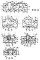
- Fig. 5 shows a modified form of display module 40 in accordance with this invention in which the light conductive panel 41 comprises a continuous, flexible optically clear panel with protrusions 43 thereon which form the key pads 6', thus eliminating the need for a separate key pad membrane.
- the switching function is accomplished by depressing the key pads 6' and thus the panel 41 into pressure engagement with domes 44 therebeneath.
- the domes 44 are bimetallic springs which are stable in the convex position shown in Fig. 5. However, when pressure is applied to the domes 44 through the key pads 6', the domes snap to a flat position, giving a tactile feedback and shorting out associated conductors 27 on the PCB to complete the switching function.
- the light conductive panel 41 may include annular protrusions 47 on the bottom surface thereof surrounding the domes 44 for keeping or retaining the domes in overlying relation to the associated conductors 27 on the PCB.
- Light conducted to the key pads 6' exits at the key pad legends 36' by any number of ways, such as scattering from deformities 48 on the key pads or refraction.
- Fig. 6 shows another form of display module 50 in accordance with this invention which also includes a flexible, optically clear light conductive panel 51 having protrusions 52 thereon forming the key pads 6'.
- recesses 53 are provided in the bottom side of the panel 51 in line with the key pad protrusions 52. Within the recesses 53 are conductors 54. When the key pads 6' are depressed, the conductors 54 make contact with associated switch contacts 27 on the PCB 12, shorting them out to complete the switching function.
- light conducted to the key pads 6' exits at the key pad legends 36' by scattering from deformities 48 or refraction in the manner previously described.
- Fig. 7 shows a modified form of display module 60 in accordance with this invention in which a conductive trace 61 of the PCB is printed on the top surface 62 of a flexible or rigid light conductive panel 63 thus eliminating the need for the PCB.
- On the bottom surface 66 of the panel 63 directly opposite the conductive trace 61 are deformities 64 for causing a portion of the light to be directed back through the panel and emitted from the light emitting area 65 immediately behind the LCD 5 in a predetermined pattern.
- the bottom surface 66 of the panel may also be provided with a reflective coating 67 in order to improve light output efficiency of the panel by reflecting any light emitted from the bottom surface back through the panel for emission from the light emitting area 65.
- Fig. 8 shows another form of display module 70 in accordance with this invention in which a conductive trace 71 of the PCB is printed on the top surface 72 of a flexible or rigid light conductive panel 73 for selective contact by conductors 74 on the key pads 75, thus eliminating the need for the PCB.
- On the bottom surface 76 of the panel 73 directly opposite the key pads 75 are deformities 77 for causing a portion of the light to be directed back through the panel for backlighting the key pads.
- a reflective coating 78 may also be provided on such bottom surface 76 for redirecting any light emitted from the bottom surface back through the panel.
- Fig. 9 shows still another form of display module 80 in accordance with this invention in which the liquid crystal material 81 of an LCD 82 is disposed between the top glass layer 83 and a bottom layer 84 formed by a light emitting area 85 of a flexible or rigid light conductive panel 86.
- the bottom layer of the LCD provides the desired backlighting for the LCD.
- the deformities 87 for causing a portion of the light to be emitted for backlighting the LCD 82 are provided on the bottom surface 88 of the panel.
- a reflective coating 89 on such bottom surface redirects any light emitted from the bottom surface back through the panel.
- Polarizing films may be provided on the top glass layer 83 of the LCD 82 and between the liquid crystal material 81 and the light conductive panel 86.
Description
- This invention relates generally to integrated display panel assemblies of the type that include backlight assemblies for backlighting two or more displays associated therewith.
- It is generally known to provide backlighting for integrated display panel assemblies and the like. This invention relates to certain improvements in the backlight assemblies for such displays which provide more efficient distribution of light to illuminate the displays associated therewith and provide support for the associated displays. As used herein, the term displays means any type of image, key pad, switch and/or legend on a display panel assembly.
-
Document GB 2 285 518 A discloses a backlight assembly for a liquid crystal display and a keyboard. - In accordance with the first aspect of the present invention, there is provided a display panel assembly comprising a light conducting panel having opposite sides and an end portion for receiving light from one or more light sources for conduction through said panel, a first light output area on one of said sides closest to said end portion underlying a liquid crystal display from which a portion of the conducted light received from said end portion is emitted from said panel for backlighting said liquid crystal display while the remaining portion of the conducted light received from said end portion passes beneath said first light output area to an other light output area on said panel further axially spaced from said end portion where additional light received from said end portion is emitted from said panel for lighting key pads of a keyboard overlying said other light output area.
- In accordance with another aspect of the invention, the integral display panel assemblies include backlight assemblies for providing efficient distribution of backlight illumination to two or more displays such as a liquid crystal diode (LCD) and a keyboard of a hand held instrument such as a cellular phone or other such device.
- In accordance with another aspect of the invention, the displays are supported by the backlight assembly.
- In accordance with another aspect of the invention, the backlight assembly includes a first light emitting area located directly behind an LCD for causing a portion of the light traveling through the backlight assembly to be emitted for backlighting the LCD and causing additional light to pass beneath the first light emitting area to other light emitting areas of the backlight assembly for illuminating one or more other displays on the display panel assembly.
- In accordance with another aspect of the invention, a plurality of light emitting diodes (LEDs) are mounted at or near one end of the backlight assembly to provide the light source for illuminating the associated displays.
- In accordance with another aspect of the invention, the backlight assembly includes slots for holding and aligning conductors such as zebra strips that extend through the slots and electrically connect an LCD or other display to a printed circuit board (PCB) mounted on the back side of the backlight assembly.
- In accordance with another aspect of the invention, a conductive trace may be provided on the front side of the backlight assembly for establishing electrical contact with an LCD or other type of display such as a key pad for performing a switching function.
- In accordance with another aspect of the invention, the backlight assembly forms the bottom layer of an LCD.
- To the accomplishment of the foregoing and related ends, the invention, then, comprises the features hereinafter fully described and particularly pointed out in the claims, the following description and the annexed drawings setting forth in detail certain illustrative embodiments of the invention, these being indicative, however, of but several of the various ways in which the principles of the invention may be employed.
- In the annexed drawings:
- Fig. 1 is a schematic top plan view of one form of integrated display panel assembly in accordance with the invention;
- Fig. 2 is a longitudinal section through the assembly of Fig. 1 taken generally along the plane of the line 2-2 thereof;
- Fig. 3 is a top plan view of the backlight assembly for the integrated display panel assembly of Figs. 1 and 2 as generally seen from the plane of the line 3-3 of Fig. 2;
- Fig. 4 is an enlarged schematic fragmentary section of a portion of the panel assembly of Fig. 2 in which an LCD and key pad are shown being backlighted by the backlight assembly;
- Figs. 5 and 6 are enlarged schematic fragmentary sections of portions of other panel assembly embodiments in accordance with this invention in which key pads or other displays are integrally formed on the backlight assemblies; and
- Figs. 7 through 9 are enlarged schematic fragmentary sections through modified forms of panel assemblies in accordance with this invention.
- Referring now in detail to the drawings and initially to Figs. 1 and 2, there is schematically shown one form of integrated display panel assembly or module 1 in accordance with the present invention including a
low profile keyboard 2 such as used in a cellular phone or other hand heldinstrument 3 and a backlight assembly 4 which provides backlight illumination for two or more displays such as a liquid crystal display (LCD) 5 andkey pads 6 on thekeyboard 2 as described hereafter. The display module 1 includes abezel 7 which serves as a frame for theLCD 5 andkey pads 6. Posts orprotuberances 10 on the front side of the backlight assembly 4 provide for alignment and attachment of the bezel, LCD and keyboard layers to the backlight assembly. Similar posts or protuberances 11 on the back side of the backlight assembly provide for alignment and attachment of a printed circuit board (PCB) 12 to such back side using suitable fasteners (not shown). - Conductive traces on the
PCB 12 may be electrically connected to theLCD 5 via elastomeric anisotropicconductive sheets 15, commonly referred to as zebra strips.Slots 16 are provided in the backlight assembly 4 (see Figs. 2 and 3) through which thezebra strips 15 extend for holding and aligning the zebra strips with respect to theLCD 5 andPCB 12. The alignment of these elements is critical in providing the required electrical connections between the LCD and PCB which are mechanically mounted on opposite sides of backlight assembly 4. - Backlight assembly 4 comprises a relatively thin,
long panel 17 made of a transparent light conductive material of any suitable type including plastic such as acrylic or polycarbonate, or glass. The lightconductive panel 17 may be substantially flat, or curved, may be a single layer or multi-layers, and may have different thicknesses and shapes. Moreover, thepanel 17 may be flexible, or rigid, and may be made out of a variety of compounds. Further, thepanel 17 may be hollow, filled with liquid, air, or be solid, and there may be holes or ridges in the panel.Panel 17 acts as a light guide for conducting light entering the panel at one or both ends via internal reflections within the panel. A portion of the light is extracted from thepanel 17 for backlighting theLCD 5 when needed while the remaining portion of the light passes beneath the LCD for lighting thekey pads 6 or other displays. - The surface luminance and uniformity of the escaping light is a function of the type, location and size of deformities or disruptions in the
panel 17. A pattern of such light extracting deformities or disruptions may be provided on selected areas on one or both sides of the panel as desired. As used herein, the terms deformities or disruptions are used interchangeably to mean any change in the shape or geometry of the panel surface and/or coating or surface treatment that causes a portion of the light to be emitted. A pattern of light extracting deformities may include a variable pattern which breaks up the light rays such that the internal angle of reflection of a portion of the light rays will be great enough to cause a portion of the light rays either to be emitted out of the panel through the side on which the light extracting deformities are provided or reflected back through the panel and emitted out the other side. - These deformities or disruptions can be produced in a variety of manners, for example, by providing a painted pattern, an etched pattern, machined pattern, a printed pattern, a hot stamped pattern, or a molded pattern or the like on selected light output areas of the panel. An ink or printed pattern may be applied for example by pad printing, silk screening, ink jet, heat transfer film process or the like. The deformities may also be printed on a sheet or film which is used to apply the deformities to the panel. This sheet or film may become a permanent part of the panel for example by attaching or otherwise positioning the sheet or film against one or both sides of the panel in order to produce a desired effect.
- By varying the density, opaqueness or translucence, shape, depth, color, area, index of refraction or type of deformities on an area or areas of the panel, the light output from the panel can be controlled. The deformities or disruptions may be used to control the percent of light emitting from any area of the panel. For example, less and/or smaller size deformities may be placed on panel areas where less light output is wanted. Conversely, a greater percentage of and/or larger deformities may be placed on areas of the panel where greater light output is desired.
- Varying the percentages and/or size of deformities in different areas of the panel is necessary in order to provide a uniform light output distribution at the different areas. For example, the amount of light traveling through the panel will ordinarily be greater in areas closer to the light source than in other areas further removed from the light source. A pattern of light extracting deformities may be used to adjust for the light variances within the panel, for example, by providing a denser concentration of light extracting deformities with increased distance from the light source thereby resulting in a more uniform light output distribution from the panel.
- The deformities may also be used to control the output ray angle distribution of the emitted light to suit a particular application. For example, where the panel is used to provide an LCD backlight, the light output will be more efficient if the deformities cause the light rays to emit from the panel at predetermined ray angles such that they will pass through the LCD with low loss.
- Additionally, the pattern of light extracting deformities may be used to adjust for light output variances attributed to light extractions of the panel. The pattern of light extracting deformities may be printed on the light output areas utilizing a wide spectrum of paints, inks, coatings, epoxies, or the like, ranging from glossy to opaque or both, and may employ half-tone separation techniques to vary the deformity coverage. Moreover, the pattern of light extracting deformities may be multiple layers or vary in index of refraction.
- Print patterns of light extracting deformities may vary in shape such as dots, squares, diamonds, ellipses, stars, random shapes, and the like. Additionally, the deformities may vary in shape and/or size along the length and/or width of the light output areas of the panel. Also, a random placement pattern of deformities may be utilized throughout the length and/or width of the light output areas of the panel. The deformities may have shapes or a pattern with no specific angle to reduce moire or other interference effects. Examples of methods to create these random patterns are printing a pattern of shapes using strochastic print pattern techniques, frequency modulated half tone patterns, or random dot half tones. Moreover, the deformities may be colored in order to effect color correction in the panel. The colors of the deformities may also vary throughout the panel, for example, to provide different colors for the same or different light output areas.
- In addition to or in lieu of the patterns of light extracting deformities previously described, other light extracting deformities including prismatic surfaces, depressions or raised surfaces of various shapes using more complex shapes in a mold pattern may be molded, etched, stamped, thermoformed, hot stamped or the like into or on one or more light output areas of the panel. Prismatic surfaces, depressions or raised surfaces will cause a portion of the light rays contacted thereby to be emitted from the panel. Also, the angles of the prisms, depressions or other surfaces may be varied to direct the light in different directions to produce a desired light output distribution or effect. Moreover, the reflective or refractive surfaces may have shapes or a pattern with no specific angles to reduce moire or other interference effects.
- The light
conductive panel 17 may have one or more light emitting diodes (LED's) or other light sources placed adjacent one or more ends or sides of the panel, or such light sources may be surface mounted on the panel or otherwise mounted interiorly of the panel. In the embodiment shown in Figs. 2 and 3, the lightconductive panel 17 has a plurality of slots, cavities oropenings 20 machined, molded or otherwise formed in one or moreoptical focus sections 21 at one end of the panel in which one or more LEDs or otherlight sources 22 are mounted. Preferably thelight sources 22 are embedded, potted or bonded in theoptical focus sections 21 in order to eliminate any air gaps or air interface surfaces between the light sources and adjacentlight transition areas 23 in order to reduce light loss received by the light transition areas and increase the light output emitted by the panel. - Such mounting of the light sources may be accomplished, for example, by bonding the light sources in the slots, cavities or
openings 20 using a sufficient quantity of a suitable optically transparent embedding, potting or bonding material. The slots, cavities oropenings 20 may be on the top, bottom, sides or ends of thelight conductor 17. Bonding can also be accomplished by a variety of methods that do not incorporate extra material, for example, thermal bonding, heat staking, ultrasonic or plastic welding or the like. Other methods of bonding include insert molding and casting around the light sources. - Also, the
light sources 22 may be multiple colored LEDs, or a combination of multiple colored radiation sources in order to provide a desired colored or white light output distribution. For example, a plurality of colored lights such as LEDs of different colors (e.g., red, blue and/or green) or a single LED with multiple colored chips may be employed to create white light or any other colored light output distribution by varying the intensities of each individual colored light. - The light
conductive panel 17 shown in Figs. 1 through 3 is made of a relatively rigid transparent material, and hasholes 25 therethrough to facilitate motion ofswitch plunger portions 26 of thekey pads 6 into and out of contact withconductors 27 on thePCB 12 which is mounted on the back side of the lightconductive panel 17 as schematically shown in Figs. 2 and 4. Thekey pads 6 are an integral part of a flexible key pad membrane orpanel 28 of accordion design which gives theswitch plungers 26 some tactile feedback and returns the key pads to their original raised positions shown in Figs. 2 and 4 after being depressed to cause theconductors 29 on theswitch plungers 26 to short out the associatedconductors 27 on the PCB. While the key pads are shown in Figs. 1 through 3 as being push type switches, it will be apparent that the key pads could be other types of switches. Also, the key pads could be knobs, pointers, indicators, slides, etc. for performing other functions as desired. - The light
conductive panel 17 has alight output area 30 immediately behind theLCD 5 containing light extracting deformities ordisruptions 31 for causing a portion of the light rays 32 from thelight sources 22 to be emitted for backlighting theLCD 5 as schematically shown in Fig. 4. - The remaining
portion 34 of the light rays passes through thelight conductor 17 beneath theLCD 5 and is scattered into theholes 25 for illuminating thekey pads 6 and associatedlegends 36. If desired, the shape of theholes 25 can be altered, ordeformities 35 can be provided around the holes to extract light in a predetermined pattern. - The relatively rigid optically
clear light conductor 17 shown in Figs. 2 through 4 performs other functions in addition to conducting light and illuminating theLCD 5 andkey pads 6 and associatedlegends 36. In particular, thelight conductor 17 serves as a spacer separating the flexible key pad membrane orpanel 28 andbezel 7 from thePCB 12 and acts as a structural member and guide for theswitch plungers 26. - Fig. 5 shows a modified form of
display module 40 in accordance with this invention in which the lightconductive panel 41 comprises a continuous, flexible optically clear panel withprotrusions 43 thereon which form the key pads 6', thus eliminating the need for a separate key pad membrane. In this embodiment, the switching function is accomplished by depressing the key pads 6' and thus thepanel 41 into pressure engagement withdomes 44 therebeneath. Thedomes 44 are bimetallic springs which are stable in the convex position shown in Fig. 5. However, when pressure is applied to thedomes 44 through the key pads 6', the domes snap to a flat position, giving a tactile feedback and shorting out associatedconductors 27 on the PCB to complete the switching function. Also, the lightconductive panel 41 may includeannular protrusions 47 on the bottom surface thereof surrounding thedomes 44 for keeping or retaining the domes in overlying relation to the associatedconductors 27 on the PCB. Light conducted to the key pads 6' exits at the key pad legends 36' by any number of ways, such as scattering fromdeformities 48 on the key pads or refraction. - Fig. 6 shows another form of
display module 50 in accordance with this invention which also includes a flexible, optically clear lightconductive panel 51 havingprotrusions 52 thereon forming the key pads 6'. However, in this embodiment recesses 53 are provided in the bottom side of thepanel 51 in line with thekey pad protrusions 52. Within therecesses 53 areconductors 54. When the key pads 6' are depressed, theconductors 54 make contact with associatedswitch contacts 27 on thePCB 12, shorting them out to complete the switching function. Here again, light conducted to the key pads 6' exits at the key pad legends 36' by scattering fromdeformities 48 or refraction in the manner previously described. - Fig. 7 shows a modified form of
display module 60 in accordance with this invention in which a conductive trace 61 of the PCB is printed on thetop surface 62 of a flexible or rigid lightconductive panel 63 thus eliminating the need for the PCB. On the bottom surface 66 of thepanel 63 directly opposite the conductive trace 61 aredeformities 64 for causing a portion of the light to be directed back through the panel and emitted from thelight emitting area 65 immediately behind theLCD 5 in a predetermined pattern. The bottom surface 66 of the panel may also be provided with a reflective coating 67 in order to improve light output efficiency of the panel by reflecting any light emitted from the bottom surface back through the panel for emission from thelight emitting area 65. - Fig. 8 shows another form of
display module 70 in accordance with this invention in which aconductive trace 71 of the PCB is printed on thetop surface 72 of a flexible or rigid light conductive panel 73 for selective contact byconductors 74 on thekey pads 75, thus eliminating the need for the PCB. On the bottom surface 76 of the panel 73 directly opposite thekey pads 75 are deformities 77 for causing a portion of the light to be directed back through the panel for backlighting the key pads. Areflective coating 78 may also be provided on such bottom surface 76 for redirecting any light emitted from the bottom surface back through the panel. - Fig. 9 shows still another form of
display module 80 in accordance with this invention in which theliquid crystal material 81 of anLCD 82 is disposed between thetop glass layer 83 and abottom layer 84 formed by alight emitting area 85 of a flexible or rigid lightconductive panel 86. Thus, in this particular embodiment, the bottom layer of the LCD provides the desired backlighting for the LCD. Also in this embodiment, thedeformities 87 for causing a portion of the light to be emitted for backlighting theLCD 82 are provided on thebottom surface 88 of the panel. A reflective coating 89 on such bottom surface redirects any light emitted from the bottom surface back through the panel. Polarizing films (not shown) may be provided on thetop glass layer 83 of theLCD 82 and between theliquid crystal material 81 and the lightconductive panel 86. - Although the invention has been shown and described with respect to certain preferred embodiments, it is obvious that equivalent alterations and modifications will occur to others skilled in the art upon the reading and understanding of the specification. The present invention includes all such equivalent alterations and modifications, and is limited only by the scope of the claims.
Claims (12)
- A display panel assembly comprising a light conducting panel having opposite sides and an end portion for receiving light from one or more light sources for conduction through said panel, a first light output area on one of said sides closest to said end portion underlying a liquid crystal display from which a portion of the conducted light received from said end portion is emitted from said panel for backlighting said liquid crystal display while the remaining portion of the conducted light received from said end portion passes beneath said first light output area to an other light output area on said panel further axially spaced from said end portion where additional light received from said end portion is emitted from said panel for lighting key pads of a keyboard overlying said other light output area.
- The assembly of claim 1 wherein said liquid crystal display and said keyboard are supported by said panel.
- The assembly of claim 2 wherein said panel includes posts for aligning and attaching said liquid crystal display and said keyboard to said panel.
- The assembly of claim 1 further comprising a circuit board attached to the other side of said panel, slots in said panel, and conductors extending through said slots for electrically connecting said liquid crystal display to said circuit board, said conductors comprising zebra strips, said slots holding and aligning said zebra strips with respect to said liquid crystal display and said circuit board.
- The assembly of claim 1 further comprising a circuit board attached to the other side of said panel, said key pads having portions extending through holes in said panel, said key pads when depressed causing contact with said circuit board to complete associated circuitry, said holes comprising said other light emitting area for causing light to be emitted around said key pads.
- The assembly of claim 5 wherein said key pads are carried by said panel which is flexible to provide tactile feedback to said key pads causing said key pads to return to their original positions when released after being depressed.
- The assembly of claim 1 wherein said key pads are on said one side of said panel, said panel being made of a flexible material, whereby when said key pads are depressed, a portion of said panel moves correspondingly.
- The assembly of claim 1 wherein said liquid crystal display includes a top layer, a bottom layer formed by said panel, and liquid crystal material between said layers, and deformities on the other side of said panel opposite said first light output area to cause a portion of the conducted light received from said end portion to be emitted from said first light output area.
- The assembly of claim 1 wherein one or more light sources are mounted in one or more recesses, slots or cavities in said end portion of said panel, said recesses, slots or cavities being filled with a transparent medium to eliminate any air interface between said light sources and said panel.
- The assembly of claim 1 wherein one or more light sources are insert molded or cast within said end portion of said panel.
- The assembly of claim 1 wherein one or more light sources are bonded to said end portion of said panel so as to eliminate any air interface between said light sources and said panel.
- The assembly of claim 1 further comprising a conductive trace on said one side of said panel, and conductors for establishing electrical contact between said liquid crystal display or said key pads and said conductive trace.
Applications Claiming Priority (2)
| Application Number | Priority Date | Filing Date | Title |
|---|---|---|---|
| US08/871,391 US5975711A (en) | 1995-06-27 | 1997-06-09 | Integrated display panel assemblies |
| US871391 | 1997-06-09 |
Publications (3)
| Publication Number | Publication Date |
|---|---|
| EP0884525A2 EP0884525A2 (en) | 1998-12-16 |
| EP0884525A3 EP0884525A3 (en) | 1998-12-23 |
| EP0884525B1 true EP0884525B1 (en) | 2006-08-30 |
Family
ID=25357345
Family Applications (1)
| Application Number | Title | Priority Date | Filing Date |
|---|---|---|---|
| EP98303885A Expired - Lifetime EP0884525B1 (en) | 1997-06-09 | 1998-05-18 | Integrated display panel assembly |
Country Status (5)
| Country | Link |
|---|---|
| US (1) | US5975711A (en) |
| EP (1) | EP0884525B1 (en) |
| JP (1) | JP4779065B2 (en) |
| DE (1) | DE69835719T2 (en) |
| TW (1) | TWM262652U (en) |
Cited By (1)
| Publication number | Priority date | Publication date | Assignee | Title |
|---|---|---|---|---|
| US8186889B2 (en) | 2007-03-30 | 2012-05-29 | Hitachi Chemical Co., Ltd. | Optical connecting member and display apparatus |
Families Citing this family (166)
| Publication number | Priority date | Publication date | Assignee | Title |
|---|---|---|---|---|
| KR0169444B1 (en) * | 1996-07-11 | 1999-01-15 | 김광호 | Display device |
| JPH10145476A (en) * | 1996-11-08 | 1998-05-29 | Casio Comput Co Ltd | Electronic equipment with display part and operating part |
| JP2000235183A (en) * | 1999-02-16 | 2000-08-29 | Matsushita Electric Ind Co Ltd | Illuminator and portable information equipment provided with the same |
| JP2000267093A (en) * | 1999-03-19 | 2000-09-29 | Matsushita Electric Ind Co Ltd | Illumination device and portable information equipment having the same |
| US6217183B1 (en) | 1999-09-15 | 2001-04-17 | Michael Shipman | Keyboard having illuminated keys |
| US7193536B2 (en) * | 1999-09-15 | 2007-03-20 | Michael Shipman | Illuminated keyboard |
| US7172303B2 (en) * | 1999-09-15 | 2007-02-06 | Michael Shipman | Illuminated keyboard |
| US20090201179A1 (en) | 1999-09-15 | 2009-08-13 | Michael Shipman | Illuminated keyboard |
| US7193535B2 (en) * | 1999-09-15 | 2007-03-20 | Michael Shipman | Illuminated keyboard |
| US20080143560A1 (en) * | 1999-09-15 | 2008-06-19 | Michael Shipman | Lightpipe for illuminating keys of a keyboard |
| US7283066B2 (en) * | 1999-09-15 | 2007-10-16 | Michael Shipman | Illuminated keyboard |
| US10013075B2 (en) | 1999-09-15 | 2018-07-03 | Michael Shipman | Illuminated keyboard |
| US6918677B2 (en) * | 1999-09-15 | 2005-07-19 | Michael Shipman | Illuminated keyboard |
| US6422712B1 (en) | 1999-09-27 | 2002-07-23 | Jaako Nousiainen | User-interface illuminator |
| DE19957611A1 (en) * | 1999-11-30 | 2001-06-07 | Osram Opto Semiconductors Gmbh | Lighting arrangement |
| DE60033264T2 (en) * | 1999-12-28 | 2007-11-08 | Fujitsu Kasei Ltd., Yokohama | Lighting apparatus for display |
| JP4352609B2 (en) * | 2000-02-25 | 2009-10-28 | セイコーエプソン株式会社 | Lighting device |
| DE10011800B4 (en) * | 2000-03-14 | 2007-11-29 | Robert Bosch Gmbh | lighting device |
| US7546141B2 (en) * | 2000-05-23 | 2009-06-09 | Robert Leon | Hybrid communication system and method |
| DE10034771A1 (en) * | 2000-07-18 | 2002-01-31 | Mannesmann Vdo Ag | Switching device for an electrical device |
| JP2002217457A (en) * | 2001-01-12 | 2002-08-02 | Nec Corp | Mobile phone, and diffusing body and lighting system provided therein |
| KR100959356B1 (en) * | 2001-06-12 | 2010-05-20 | 웰스테트 테라퓨틱스 코포레이션 | Compounds for the Treatment of Metabolic Disorders |
| US6950680B2 (en) * | 2001-09-17 | 2005-09-27 | Nokia Corporation | Electronic device |
| US6561659B1 (en) * | 2001-11-15 | 2003-05-13 | Wintek Corporation | Photoconductor panel for lighting a keyboard |
| JP2003151393A (en) * | 2001-11-15 | 2003-05-23 | Matsushita Electric Ind Co Ltd | Movable contact body for panel switch, panel switch using the same and electronic equipment mounting with the panel switch |
| US6827459B2 (en) * | 2002-03-27 | 2004-12-07 | 3M Innovative Properties Company | Lighted fastening structure |
| FI113594B (en) | 2002-04-12 | 2004-05-14 | Nokia Corp | Switch Arrangement and Keyboard Switch Matrix Structure |
| US6926418B2 (en) * | 2002-04-24 | 2005-08-09 | Nokia Corporation | Integrated light-guide and dome-sheet for keyboard illumination |
| DE50308334D1 (en) * | 2002-05-07 | 2007-11-22 | Schott Ag | Lighting device for buttons |
| EP1376166B1 (en) * | 2002-06-19 | 2011-05-25 | Kabushiki Kaisha Tokai-Rika-Denki-Seisakusho | Sheet-switch device |
| JP4462817B2 (en) * | 2002-08-01 | 2010-05-12 | 日本電気株式会社 | Visualization method of character input mode by key backlight multicolor lighting |
| DE10236718A1 (en) * | 2002-08-06 | 2004-02-12 | E.G.O. Control Systems Gmbh & Co. Kg | Washing machine, tumble drier or dishwasher with optical display for operating data has panel with section of reduced thickness, on which display is mounted, and light source below it |
| US7671859B2 (en) * | 2002-11-06 | 2010-03-02 | Continental Automotive Systems Us, Inc. | Thin instrument cluster with anti-reflective coating |
| EP1418734B1 (en) * | 2002-11-06 | 2007-12-12 | Sony Ericsson Mobile Communications AB | Means for illuminating keypad and device incorporating same |
| US6975369B1 (en) * | 2002-12-12 | 2005-12-13 | Gelcore, Llc | Liquid crystal display with color backlighting employing light emitting diodes |
| EP1573374B1 (en) | 2002-12-16 | 2007-02-28 | Casio Computer Co., Ltd. | Illumination device and electronic apparatus |
| JP4178937B2 (en) * | 2002-12-16 | 2008-11-12 | カシオ計算機株式会社 | Lighting device and electronic device |
| US7417782B2 (en) | 2005-02-23 | 2008-08-26 | Pixtronix, Incorporated | Methods and apparatus for spatial light modulation |
| JP4186664B2 (en) * | 2003-03-24 | 2008-11-26 | 松下電器産業株式会社 | Switch device |
| TWI321248B (en) * | 2003-05-12 | 2010-03-01 | Au Optronics Corp | Led backlight module |
| US7044627B2 (en) * | 2003-05-30 | 2006-05-16 | Mertz John C | Display retainer and backlight |
| US7755506B1 (en) | 2003-09-03 | 2010-07-13 | Legrand Home Systems, Inc. | Automation and theater control system |
| EP1665311B1 (en) * | 2003-09-08 | 2013-06-26 | Chimei InnoLux Corporation | A body and an electronic device |
| US6861600B1 (en) | 2003-10-01 | 2005-03-01 | Lumitex, Inc. | Integrated switch and backlight assembly |
| US20050073826A1 (en) * | 2003-10-06 | 2005-04-07 | Kuo Heng Sheng | Light guide plate with multiple visible regions |
| JP4382432B2 (en) | 2003-10-10 | 2009-12-16 | スタンレー電気株式会社 | Self-illuminating pushbutton input device |
| AU2003274188A1 (en) * | 2003-10-23 | 2005-05-11 | Nokia Corporation | Keyboard with key supporting structure for portable electronics devices |
| EP1558009A1 (en) * | 2004-01-22 | 2005-07-27 | Sony Ericsson Mobile Communications AB | Portable electronic equipment having an illuminated area |
| DE102004052932B4 (en) * | 2004-10-29 | 2007-09-20 | Klawonn, Joachim, Dipl.-Ing.(FH) | sensor field |
| US11216078B2 (en) | 2005-01-18 | 2022-01-04 | Michael Shipman | Illuminated keyboard |
| US20070205969A1 (en) | 2005-02-23 | 2007-09-06 | Pixtronix, Incorporated | Direct-view MEMS display devices and methods for generating images thereon |
| US7999994B2 (en) | 2005-02-23 | 2011-08-16 | Pixtronix, Inc. | Display apparatus and methods for manufacture thereof |
| US8482496B2 (en) | 2006-01-06 | 2013-07-09 | Pixtronix, Inc. | Circuits for controlling MEMS display apparatus on a transparent substrate |
| US9158106B2 (en) | 2005-02-23 | 2015-10-13 | Pixtronix, Inc. | Display methods and apparatus |
| US9261694B2 (en) | 2005-02-23 | 2016-02-16 | Pixtronix, Inc. | Display apparatus and methods for manufacture thereof |
| US7502159B2 (en) | 2005-02-23 | 2009-03-10 | Pixtronix, Inc. | Methods and apparatus for actuating displays |
| US9082353B2 (en) | 2010-01-05 | 2015-07-14 | Pixtronix, Inc. | Circuits for controlling display apparatus |
| US8159428B2 (en) | 2005-02-23 | 2012-04-17 | Pixtronix, Inc. | Display methods and apparatus |
| US7271945B2 (en) | 2005-02-23 | 2007-09-18 | Pixtronix, Inc. | Methods and apparatus for actuating displays |
| US7405852B2 (en) | 2005-02-23 | 2008-07-29 | Pixtronix, Inc. | Display apparatus and methods for manufacture thereof |
| US7616368B2 (en) | 2005-02-23 | 2009-11-10 | Pixtronix, Inc. | Light concentrating reflective display methods and apparatus |
| US7742016B2 (en) | 2005-02-23 | 2010-06-22 | Pixtronix, Incorporated | Display methods and apparatus |
| US7675665B2 (en) | 2005-02-23 | 2010-03-09 | Pixtronix, Incorporated | Methods and apparatus for actuating displays |
| US7755582B2 (en) | 2005-02-23 | 2010-07-13 | Pixtronix, Incorporated | Display methods and apparatus |
| US9229222B2 (en) | 2005-02-23 | 2016-01-05 | Pixtronix, Inc. | Alignment methods in fluid-filled MEMS displays |
| US7746529B2 (en) | 2005-02-23 | 2010-06-29 | Pixtronix, Inc. | MEMS display apparatus |
| US7304785B2 (en) | 2005-02-23 | 2007-12-04 | Pixtronix, Inc. | Display methods and apparatus |
| US8519945B2 (en) | 2006-01-06 | 2013-08-27 | Pixtronix, Inc. | Circuits for controlling display apparatus |
| US8310442B2 (en) | 2005-02-23 | 2012-11-13 | Pixtronix, Inc. | Circuits for controlling display apparatus |
| US7304786B2 (en) | 2005-02-23 | 2007-12-04 | Pixtronix, Inc. | Methods and apparatus for bi-stable actuation of displays |
| US7525534B2 (en) | 2005-03-14 | 2009-04-28 | Palm, Inc. | Small form-factor keypad for mobile computing devices |
| US7511700B2 (en) * | 2005-03-14 | 2009-03-31 | Palm, Inc. | Device and technique for assigning different inputs to keys on a keypad |
| US9142369B2 (en) | 2005-03-14 | 2015-09-22 | Qualcomm Incorporated | Stack assembly for implementing keypads on mobile computing devices |
| DE102005013804A1 (en) * | 2005-03-24 | 2006-09-28 | BSH Bosch und Siemens Hausgeräte GmbH | Illuminated display window for LED and / or LC displays |
| KR100629053B1 (en) * | 2005-05-19 | 2006-09-26 | 삼성전자주식회사 | Key-pad assembly |
| US7394030B2 (en) * | 2005-06-02 | 2008-07-01 | Palm, Inc. | Small form-factor keyboard using keys with offset peaks and pitch variations |
| CN100376969C (en) * | 2005-06-03 | 2008-03-26 | 鸿富锦精密工业(深圳)有限公司 | Light guiding component, and backlight module set of using the component |
| US8718437B2 (en) | 2006-03-07 | 2014-05-06 | Qd Vision, Inc. | Compositions, optical component, system including an optical component, devices, and other products |
| KR100689395B1 (en) * | 2005-07-06 | 2007-03-02 | 삼성전자주식회사 | Key pad assembly |
| KR100639954B1 (en) * | 2005-07-12 | 2006-11-01 | 주식회사 엘에스텍 | A back light unit having flexibility for the key of the input devices |
| TWM286375U (en) * | 2005-08-08 | 2006-01-21 | Inventec Corp | Light guiding structure |
| US7294802B2 (en) * | 2005-08-13 | 2007-11-13 | Palm, Inc. | Lighting and usability features for key structures and keypads on computing devices |
| US7275836B2 (en) | 2005-08-13 | 2007-10-02 | Palm, Inc. | Lighting and usability features for key structures and keypads on computing devices |
| US8690368B1 (en) | 2005-08-22 | 2014-04-08 | Michael Shipman | Cavity filled lightpipe for illuminating keys of a keyboard |
| US7778262B2 (en) | 2005-09-07 | 2010-08-17 | Vantage Controls, Inc. | Radio frequency multiple protocol bridge |
| KR100787581B1 (en) * | 2005-09-27 | 2007-12-21 | 삼성전자주식회사 | Keypad having phosphor, keypad assembly and portable terminal |
| US7588338B2 (en) * | 2005-11-29 | 2009-09-15 | Zippy Technology Corp. | Keyboard equipped with a backlight structure |
| CN2874591Y (en) * | 2005-12-30 | 2007-02-28 | 鸿富锦精密工业(深圳)有限公司 | Computer panel light conductive device |
| US8526096B2 (en) | 2006-02-23 | 2013-09-03 | Pixtronix, Inc. | Mechanical light modulators with stressed beams |
| US8849087B2 (en) | 2006-03-07 | 2014-09-30 | Qd Vision, Inc. | Compositions, optical component, system including an optical component, devices, and other products |
| US9874674B2 (en) | 2006-03-07 | 2018-01-23 | Samsung Electronics Co., Ltd. | Compositions, optical component, system including an optical component, devices, and other products |
| TWM298289U (en) * | 2006-03-17 | 2006-09-21 | Hon Hai Prec Ind Co Ltd | Light guide plates and electronic products using the same |
| WO2007117668A2 (en) | 2006-04-07 | 2007-10-18 | Qd Vision, Inc. | Methods and articles including nanomaterial |
| FR2900220B1 (en) * | 2006-04-24 | 2008-07-18 | Valeo Vision Sa | LIGHTING OR SIGNALING DEVICE WITH DEPTH EFFECT. |
| US7876489B2 (en) | 2006-06-05 | 2011-01-25 | Pixtronix, Inc. | Display apparatus with optical cavities |
| US7967459B2 (en) * | 2006-06-14 | 2011-06-28 | Bea, Inc. | Activation device |
| WO2008003814A1 (en) * | 2006-07-03 | 2008-01-10 | Nokia Corporation | Changing graphics in an apparatus including user interface illumination |
| US7551077B2 (en) * | 2006-07-31 | 2009-06-23 | Alcon, Inc. | RFID ring illumination system for surgical machine |
| JP4926762B2 (en) * | 2006-08-03 | 2012-05-09 | シチズン電子株式会社 | Luminescent sheet module |
| JP4668867B2 (en) * | 2006-08-09 | 2011-04-13 | 株式会社東海理化電機製作所 | Operating device |
| US7498534B2 (en) * | 2006-08-30 | 2009-03-03 | 3M Innovative Properties Company | Keypad light guide |
| US8989822B2 (en) | 2006-09-08 | 2015-03-24 | Qualcomm Incorporated | Keypad assembly for use on a contoured surface of a mobile computing device |
| KR101243669B1 (en) * | 2006-10-18 | 2013-03-25 | 엘지전자 주식회사 | Mobile terminal |
| EP2080045A1 (en) | 2006-10-20 | 2009-07-22 | Pixtronix Inc. | Light guides and backlight systems incorporating light redirectors at varying densities |
| CN101606090B (en) | 2006-11-14 | 2012-09-05 | 莫迪里斯有限公司 | Lightguide arrangement and related applications |
| US20080117635A1 (en) * | 2006-11-17 | 2008-05-22 | Ko-Ju Chen | Multi-Layer Light Guiding Structure And Method For Using The Same |
| TWI329483B (en) * | 2006-11-30 | 2010-08-21 | Lite On Technology Corp | Thin light-guiding structure and electronic device using the same |
| TW200825459A (en) * | 2006-12-08 | 2008-06-16 | Jia-Hua Jang | Optical film with optical points |
| US9176318B2 (en) | 2007-05-18 | 2015-11-03 | Pixtronix, Inc. | Methods for manufacturing fluid-filled MEMS displays |
| US7852546B2 (en) | 2007-10-19 | 2010-12-14 | Pixtronix, Inc. | Spacers for maintaining display apparatus alignment |
| US20080205082A1 (en) * | 2007-02-23 | 2008-08-28 | Silitech Technology Corp. | Super-thin light-guiding module with a side light-projecting type function |
| US8471832B2 (en) * | 2007-03-02 | 2013-06-25 | Samsung Electronics Co., Ltd. | Keypad assembly having light leakage prevention structure |
| US7534001B2 (en) * | 2007-03-07 | 2009-05-19 | Ichia Technologies, Inc. | Light-guiding method of light-guiding plate and key pad assembly using the light-guiding plate |
| US20080310185A1 (en) * | 2007-06-15 | 2008-12-18 | Motorola, Inc. | Addressable lighting element for a mobile communication device |
| JP2010533976A (en) * | 2007-07-18 | 2010-10-28 | キユーデイー・ビジヨン・インコーポレーテツド | Quantum dot-based light sheet useful for solid-state lighting |
| WO2009014707A2 (en) | 2007-07-23 | 2009-01-29 | Qd Vision, Inc. | Quantum dot light enhancement substrate and lighting device including same |
| JP5083954B2 (en) * | 2007-08-23 | 2012-11-28 | シチズン電子株式会社 | Film-shaped light guide plate unit, planar light unit, display device, and electronic apparatus |
| US8128249B2 (en) | 2007-08-28 | 2012-03-06 | Qd Vision, Inc. | Apparatus for selectively backlighting a material |
| US20090067194A1 (en) * | 2007-09-11 | 2009-03-12 | World Properties, Inc. | Light guide with imprinted phosphor |
| JP2009070719A (en) * | 2007-09-14 | 2009-04-02 | Citizen Electronics Co Ltd | Light guide body and electronic equipment |
| DE102007044360A1 (en) | 2007-09-17 | 2009-03-19 | Robert Bosch Gmbh | Improved lighting for adjusting knob of a gauge |
| JP2009129560A (en) * | 2007-11-20 | 2009-06-11 | Kuraray Co Ltd | Illuminating device of electronic apparatus |
| TWI394110B (en) * | 2007-12-14 | 2013-04-21 | Chi Mei Comm Systems Inc | Icon dispaly |
| US20090179870A1 (en) * | 2008-01-16 | 2009-07-16 | World Properties, Inc. | Luminous touch screen with interstitial layers |
| JP2009205940A (en) * | 2008-02-28 | 2009-09-10 | Panasonic Corp | Light guide sheet, and moving contact body using it |
| US8248560B2 (en) | 2008-04-18 | 2012-08-21 | Pixtronix, Inc. | Light guides and backlight systems incorporating prismatic structures and light redirectors |
| US9207385B2 (en) | 2008-05-06 | 2015-12-08 | Qd Vision, Inc. | Lighting systems and devices including same |
| EP2297762B1 (en) | 2008-05-06 | 2017-03-15 | Samsung Electronics Co., Ltd. | Solid state lighting devices including quantum confined semiconductor nanoparticles |
| WO2009137053A1 (en) | 2008-05-06 | 2009-11-12 | Qd Vision, Inc. | Optical components, systems including an optical component, and devices |
| CN101604207A (en) * | 2008-06-11 | 2009-12-16 | 展晶科技(深圳)有限公司 | Illuminated keyboard |
| US8178802B2 (en) | 2008-07-31 | 2012-05-15 | Electrolux Home Products, Inc. | Unitized appliance control panel assembly and components of the assembly |
| US8520285B2 (en) | 2008-08-04 | 2013-08-27 | Pixtronix, Inc. | Methods for manufacturing cold seal fluid-filled display apparatus |
| US8169679B2 (en) | 2008-10-27 | 2012-05-01 | Pixtronix, Inc. | MEMS anchors |
| DE102008053357B4 (en) * | 2008-10-27 | 2010-08-05 | Gigaset Communications Gmbh | Electrotechnical device with a lighting arrangement for illuminating a keyboard mat and a display module |
| US8500348B2 (en) * | 2008-11-24 | 2013-08-06 | Logitech Europe S.A. | Keyboard with ultra-durable keys |
| US20100142222A1 (en) * | 2008-12-04 | 2010-06-10 | World Properties, Inc. | Light guide with refractive layer |
| US11198270B2 (en) | 2008-12-30 | 2021-12-14 | Nanosys, Inc. | Quantum dot films, lighting devices, and lighting methods |
| US10214686B2 (en) | 2008-12-30 | 2019-02-26 | Nanosys, Inc. | Methods for encapsulating nanocrystals and resulting compositions |
| US8343575B2 (en) | 2008-12-30 | 2013-01-01 | Nanosys, Inc. | Methods for encapsulating nanocrystals and resulting compositions |
| KR101869923B1 (en) | 2009-08-14 | 2018-07-20 | 삼성전자주식회사 | Lighting devices, an optical component for a lighting device, and methods |
| DE102009051617B3 (en) * | 2009-11-02 | 2011-04-28 | Pas Deutschland Gmbh | Button for an operating arrangement, as well as operating arrangement and household appliance |
| EP2322962A1 (en) * | 2009-11-17 | 2011-05-18 | Weidmann Plastics Technology AG | Decorating element with an optical light guide |
| TWI401717B (en) | 2009-12-28 | 2013-07-11 | Darfon Electronics Corp | Masking, backlight module, and lighting keyboard |
| BR112012019383A2 (en) | 2010-02-02 | 2017-09-12 | Pixtronix Inc | CIRCUITS TO CONTROL DISPLAY APPARATUS |
| US8350728B2 (en) | 2010-04-23 | 2013-01-08 | Hewlett-Packard Development Company, L.P. | Keyboard with integrated and numeric keypad |
| CN102338348A (en) * | 2010-07-21 | 2012-02-01 | 深圳富泰宏精密工业有限公司 | Light guide assembly |
| US8371734B2 (en) | 2010-09-17 | 2013-02-12 | Rogers Corporation | Front lit alterable display |
| EP3540300A1 (en) | 2010-11-10 | 2019-09-18 | Nanosys, Inc. | Quantum dot films, lighting devices, and lighting methods |
| TWI430310B (en) * | 2010-12-20 | 2014-03-11 | Primax Electronics Ltd | Luminous keyboard |
| US9189078B2 (en) * | 2010-12-20 | 2015-11-17 | Apple Inc. | Enhancing keycap legend visibility with optical components |
| US9071676B2 (en) | 2011-02-03 | 2015-06-30 | Bayer Healthcare Llc | Component illumination apparatus, systems, and electronic devices and methods of manufacturing and using same |
| US9677722B2 (en) | 2011-02-25 | 2017-06-13 | Lumitex, Inc. | Flat optical fiber lighting assembly with integrated electrical circuitry |
| CN103037649B (en) * | 2011-10-06 | 2015-09-30 | 鸿富锦精密工业(武汉)有限公司 | Electronic installation |
| TWI477952B (en) * | 2012-04-06 | 2015-03-21 | Compal Electronics Inc | Electronic device |
| TWM448778U (en) * | 2012-11-02 | 2013-03-11 | Darfon Electronics Corp | Protective cover and keyboard |
| US9091411B2 (en) | 2012-11-02 | 2015-07-28 | Osram Sylvania Inc. | Illumination techniques and devices |
| US9134552B2 (en) | 2013-03-13 | 2015-09-15 | Pixtronix, Inc. | Display apparatus with narrow gap electrostatic actuators |
| US10166402B2 (en) | 2013-05-16 | 2019-01-01 | Excelitas Technologies Corp. | Visible light photo-disinfection patch |
| WO2015191418A1 (en) * | 2014-06-10 | 2015-12-17 | Corning Incorporated | Patterned glass light guide and display device comprising the same |
| US10405758B2 (en) | 2014-11-07 | 2019-09-10 | Welch Allyn, Inc. | Carrier assembly for blood pressure module |
| FR3030797B1 (en) | 2014-12-17 | 2018-05-11 | Thales | KEYBOARD WITH IMPROVED RELIABILITY |
| WO2017121516A1 (en) | 2016-01-14 | 2017-07-20 | Weidplas Gmbh | Component comprising a flat decorative element and a housing |
| US10866353B2 (en) | 2016-12-02 | 2020-12-15 | Ascensia Diabetes Care Holdings Ag | Systems, methods and apparatus for illuminating edge portions of a face of an electronic device display lens |
| EP3655289A1 (en) | 2017-07-21 | 2020-05-27 | Weidplas GmbH | Component for a vehicle |
| US10802602B2 (en) * | 2018-05-21 | 2020-10-13 | Logitech Europe S.A. | Input device with overlapping key structure |
| US10963067B2 (en) * | 2019-02-25 | 2021-03-30 | Microsoft Technology Licensing, Llc | Multilayout keyboard |
Family Cites Families (50)
| Publication number | Priority date | Publication date | Assignee | Title |
|---|---|---|---|---|
| US3328570A (en) * | 1965-04-09 | 1967-06-27 | Gen Electric | Illuminated panel member |
| US3774021A (en) * | 1972-05-25 | 1973-11-20 | Bell Telephone Labor Inc | Light emitting device |
| US3892959A (en) * | 1973-11-02 | 1975-07-01 | Gte Automatic Electric Lab Inc | Edge-lighted panel arrangement |
| JPS5226886U (en) * | 1975-08-13 | 1977-02-24 | ||
| JPS52122074U (en) * | 1976-03-10 | 1977-09-16 | ||
| CA1102767A (en) * | 1978-03-15 | 1981-06-09 | Decca Limited | Illuminated panels |
| US4282560A (en) * | 1979-01-15 | 1981-08-04 | A.C.A. Products, Inc. | Light distributor |
| US4257084A (en) * | 1979-02-21 | 1981-03-17 | Reynolds Christopher H | Display device |
| JPS5686723U (en) * | 1979-12-07 | 1981-07-11 | ||
| US4446508A (en) * | 1983-01-17 | 1984-05-01 | Plast-Ad, Inc. | Edge lighted article holder |
| US4573766A (en) * | 1983-12-19 | 1986-03-04 | Cordis Corporation | LED Staggered back lighting panel for LCD module |
| JPS6119919U (en) * | 1984-07-10 | 1986-02-05 | 日本電産コパル株式会社 | illuminated keyboard switch |
| JPS61233390A (en) * | 1985-04-09 | 1986-10-17 | 松下電器産業株式会社 | Luminaire for electronic apparatus |
| US4630895A (en) * | 1985-06-06 | 1986-12-23 | Motorola, Inc. | LCD lightguide |
| US4714983A (en) * | 1985-06-10 | 1987-12-22 | Motorola, Inc. | Uniform emission backlight |
| US4638131A (en) * | 1986-01-15 | 1987-01-20 | General Motors Corporation | Steering wheel pad keyboard switch assembly |
| US4751615A (en) * | 1986-08-07 | 1988-06-14 | International Marketing Concepts, Inc. | Page light |
| US4772769A (en) * | 1987-02-06 | 1988-09-20 | Burr-Brown Corporation | Apparatus for selective backlighting of keys of a keyboard |
| US4789224A (en) * | 1987-05-04 | 1988-12-06 | General Motors Corporation | Instrument panel having light pipe having legs |
| JPH0157785U (en) * | 1987-10-07 | 1989-04-11 | ||
| JP2603995B2 (en) * | 1988-04-21 | 1997-04-23 | 富士通株式会社 | Light guide panel |
| US5005108A (en) * | 1989-02-10 | 1991-04-02 | Lumitex, Inc. | Thin panel illuminator |
| US4978952A (en) * | 1989-02-24 | 1990-12-18 | Collimated Displays Incorporated | Flat screen color video display |
| US4974122A (en) * | 1989-03-28 | 1990-11-27 | Rockwell International Corporation | Compact LCD luminaire |
| JPH02142820U (en) * | 1989-04-28 | 1990-12-04 | ||
| DE3919925A1 (en) * | 1989-06-19 | 1990-12-20 | Inotec Gmbh Ges Fuer Innovativ | ILLUMINATED, DISPLAY UNIT, PARTICULARLY HOUSE NUMBER, TRAFFIC SIGN, ADVERTISER |
| JPH0365982A (en) * | 1989-08-03 | 1991-03-20 | Pioneer Electron Corp | Display board illuminating device for display device |
| DE3929955A1 (en) * | 1989-09-08 | 1991-03-14 | Inotec Gmbh Ges Fuer Innovativ | LIGHT SPOTLIGHTS |
| US5283673A (en) * | 1989-09-30 | 1994-02-01 | Kabushiki Kaisha Meitaku Shisutemu | Surface luminous source panel with areas having different reflector speck densities |
| US4975808A (en) * | 1989-10-02 | 1990-12-04 | Motorola, Inc. | Backlighting apparatus |
| US5093765A (en) * | 1990-02-16 | 1992-03-03 | Tosoh Corporation | Back lighting device for a panel |
| US5134549A (en) * | 1990-06-19 | 1992-07-28 | Enplas Corporation | Surface light source device |
| GB2247310B (en) * | 1990-07-03 | 1993-09-22 | Meitaku Syst Kk | Edge light panel device |
| JPH0437931U (en) * | 1990-07-25 | 1992-03-31 | ||
| US5225818A (en) * | 1990-11-26 | 1993-07-06 | Data Entry Products, Incorporated | Data entry control panel |
| US5128842A (en) * | 1991-06-03 | 1992-07-07 | Sunarrow Co., Inc. | Uniform illumination plate |
| JPH0595395A (en) * | 1991-10-01 | 1993-04-16 | Matsushita Electric Ind Co Ltd | Portable radio telephone system |
| US5349503A (en) * | 1991-12-31 | 1994-09-20 | At&T Bell Laboratories | Illuminated transparent display with microtextured back reflector |
| JPH0622017A (en) * | 1992-07-03 | 1994-01-28 | Matsushita Electric Ind Co Ltd | Telephone set with back light |
| JPH0651129A (en) * | 1992-07-27 | 1994-02-25 | Inoue Denki Kk | Illuminating device |
| US5339179A (en) * | 1992-10-01 | 1994-08-16 | International Business Machines Corp. | Edge-lit transflective non-emissive display with angled interface means on both sides of light conducting panel |
| JPH07113718B2 (en) * | 1993-03-03 | 1995-12-06 | 日本電気株式会社 | Backlight device for liquid crystal panel |
| US5390085A (en) * | 1993-11-19 | 1995-02-14 | Motorola, Inc. | Light diffuser for a liquid crystal display |
| FI95177C (en) * | 1994-01-10 | 1995-12-27 | Nokia Mobile Phones Ltd | Equipped with an illuminated keyboard front panel for an electronic device |
| WO1996017207A1 (en) * | 1994-11-29 | 1996-06-06 | Precision Lamp, Inc. | Edge light for panel display |
| US5521342A (en) * | 1994-12-27 | 1996-05-28 | General Motors Corporation | Switch having combined light pipe and printed circuit board |
| US5537300A (en) * | 1995-02-01 | 1996-07-16 | Kraco Enterprises, Inc. | Control panel |
| JPH08248420A (en) * | 1995-03-07 | 1996-09-27 | Casio Comput Co Ltd | Liquid crystal display device |
| JPH0981048A (en) * | 1995-09-14 | 1997-03-28 | Beam Denshi Kogyo Kk | Light transmission plate device |
| JP3715356B2 (en) * | 1995-09-26 | 2005-11-09 | 富士通株式会社 | Telephone |
-
1997
- 1997-06-09 US US08/871,391 patent/US5975711A/en not_active Expired - Lifetime
-
1998
- 1998-05-18 DE DE69835719T patent/DE69835719T2/en not_active Expired - Lifetime
- 1998-05-18 EP EP98303885A patent/EP0884525B1/en not_active Expired - Lifetime
- 1998-05-20 TW TW091210815U patent/TWM262652U/en not_active IP Right Cessation
- 1998-06-08 JP JP15970698A patent/JP4779065B2/en not_active Expired - Fee Related
Cited By (1)
| Publication number | Priority date | Publication date | Assignee | Title |
|---|---|---|---|---|
| US8186889B2 (en) | 2007-03-30 | 2012-05-29 | Hitachi Chemical Co., Ltd. | Optical connecting member and display apparatus |
Also Published As
| Publication number | Publication date |
|---|---|
| JP4779065B2 (en) | 2011-09-21 |
| US5975711A (en) | 1999-11-02 |
| EP0884525A3 (en) | 1998-12-23 |
| EP0884525A2 (en) | 1998-12-16 |
| DE69835719D1 (en) | 2006-10-12 |
| DE69835719T2 (en) | 2007-09-13 |
| JPH1115393A (en) | 1999-01-22 |
| TWM262652U (en) | 2005-04-21 |
Similar Documents
| Publication | Publication Date | Title |
|---|---|---|
| EP0884525B1 (en) | Integrated display panel assembly | |
| US6796668B2 (en) | Light emitting panel assemblies for use in automotive applications and the like | |
| US5618096A (en) | Light emitting panel assemblies | |
| US7703967B2 (en) | Light emitting panel assemblies | |
| KR101138321B1 (en) | Light emitting sheet module | |
| US7994445B2 (en) | Sheet switch, sheet switch module and panel switch | |
| US8188397B2 (en) | Sheet switch module |
Legal Events
| Date | Code | Title | Description |
|---|---|---|---|
| PUAI | Public reference made under article 153(3) epc to a published international application that has entered the european phase |
Free format text: ORIGINAL CODE: 0009012 |
|
| PUAL | Search report despatched |
Free format text: ORIGINAL CODE: 0009013 |
|
| AK | Designated contracting states |
Kind code of ref document: A2 Designated state(s): DE FR GB |
|
| AX | Request for extension of the european patent |
Free format text: AL;LT;LV;MK;RO;SI |
|
| AK | Designated contracting states |
Kind code of ref document: A3 Designated state(s): AT BE CH CY DE DK ES FI FR GB GR IE IT LI LU MC NL PT SE |
|
| AX | Request for extension of the european patent |
Free format text: AL;LT;LV;MK;RO;SI |
|
| 17P | Request for examination filed |
Effective date: 19990421 |
|
| AKX | Designation fees paid |
Free format text: DE FR GB |
|
| RAP1 | Party data changed (applicant data changed or rights of an application transferred) |
Owner name: SOLID STATE OPTO LIMITED |
|
| 17Q | First examination report despatched |
Effective date: 20040927 |
|
| GRAP | Despatch of communication of intention to grant a patent |
Free format text: ORIGINAL CODE: EPIDOSNIGR1 |
|
| RIC1 | Information provided on ipc code assigned before grant |
Ipc: H04M 1/22 20060101ALI20060217BHEP Ipc: G02B 6/00 20060101AFI20060217BHEP |
|
| GRAS | Grant fee paid |
Free format text: ORIGINAL CODE: EPIDOSNIGR3 |
|
| GRAA | (expected) grant |
Free format text: ORIGINAL CODE: 0009210 |
|
| AK | Designated contracting states |
Kind code of ref document: B1 Designated state(s): DE FR GB |
|
| REG | Reference to a national code |
Ref country code: GB Ref legal event code: FG4D |
|
| REF | Corresponds to: |
Ref document number: 69835719 Country of ref document: DE Date of ref document: 20061012 Kind code of ref document: P |
|
| ET | Fr: translation filed | ||
| PLBE | No opposition filed within time limit |
Free format text: ORIGINAL CODE: 0009261 |
|
| STAA | Information on the status of an ep patent application or granted ep patent |
Free format text: STATUS: NO OPPOSITION FILED WITHIN TIME LIMIT |
|
| 26N | No opposition filed |
Effective date: 20070531 |
|
| REG | Reference to a national code |
Ref country code: GB Ref legal event code: 732E Free format text: REGISTERED BETWEEN 20101104 AND 20101110 |
|
| REG | Reference to a national code |
Ref country code: FR Ref legal event code: TP |
|
| PGFP | Annual fee paid to national office [announced via postgrant information from national office to epo] |
Ref country code: DE Payment date: 20120529 Year of fee payment: 15 |
|
| PGFP | Annual fee paid to national office [announced via postgrant information from national office to epo] |
Ref country code: GB Payment date: 20120525 Year of fee payment: 15 Ref country code: FR Payment date: 20120607 Year of fee payment: 15 |
|
| GBPC | Gb: european patent ceased through non-payment of renewal fee |
Effective date: 20130518 |
|
| PG25 | Lapsed in a contracting state [announced via postgrant information from national office to epo] |
Ref country code: DE Free format text: LAPSE BECAUSE OF NON-PAYMENT OF DUE FEES Effective date: 20131203 |
|
| REG | Reference to a national code |
Ref country code: DE Ref legal event code: R119 Ref document number: 69835719 Country of ref document: DE Effective date: 20131203 |
|
| REG | Reference to a national code |
Ref country code: FR Ref legal event code: ST Effective date: 20140131 |
|
| PG25 | Lapsed in a contracting state [announced via postgrant information from national office to epo] |
Ref country code: GB Free format text: LAPSE BECAUSE OF NON-PAYMENT OF DUE FEES Effective date: 20130518 |
|
| PG25 | Lapsed in a contracting state [announced via postgrant information from national office to epo] |
Ref country code: FR Free format text: LAPSE BECAUSE OF NON-PAYMENT OF DUE FEES Effective date: 20130531 |