Field of the Invention
The present invention relates to optical-fiber-attached micromechanical devices
having a movable membrane for generating optical interference effects.
Background of the Invention
Micromechanical devices having a movable membrane for creating optical
interference effects may be used in a variety of applications. For example, such devices
are useful as high speed, inexpensive optical modulators for optical communications
systems. Using such devices in optical systems requires optical coupling to
waveguides such as optical fibers. Such optical coupling may be problematic.
In conventional arrangements for optically coupling an optical fiber to a
micromechanical device, there is a small gap between the fiber and the device.
Unfortunately, undesirable optical effects resulting in signal loss and noise may result
from the gap. Additionally, the presence of the gap complicates device packaging.
As such, there is a need for an improved method for attaching optical fibers to
micromechanical devices, and a need for the articles resulting therefrom.
According to one aspect of the present invention, there is provided an
article having an optical fiber integrally attached to a micro-device, the article
comprising: a micro-device having spaced movable and nonmoving layers: an optical
fiber attached to the micro-device, the optical fiber having an optical core in optical
communication with the nonmoving layer and the movable layer; and an integrating
arrangement for attaching the optical fiber to the micro-device, wherein the integrating
arrangement comprises a layer of adhesive that is index-matched to a refractive index of
the optical core, wherein, the moveable layer is physically adapted for moving relative
to the nonmoving layer under the influence of an actuating force, such that the relative
movement changes the space between the movable and nonmoving layers so that micro-device
reflectivity changes. The actuating force can be a pressure exerted by a fluid that
is in contact with the movable layer. The article can further comprise an instrumentality
for relating changes in reflectivity to changes in the pressure exerted by the fluid. The
movable layer can be characterized by a tensile stress that is in the range of from about
0 to 1000 MPa. The movable layer can have a cross-sectional area within the range of
from about 500 to 100,000 square microns. The movable layer can be characterized by
a first side and a second side, and a chamber can be defined between the nonmoving
layer and the first side of the movable layer, the article further comprising an evacuated
cavity located on the second side of the movable layer. The chamber can contain a gas.
The actuating force can be a pressure exerted by the gas on the movable layer, which
pressure can vary only in response to temperature changes in the gas. The article can
further comprise means for relating changes in reflectivity to changes in the temperature
of the gas. The space between the movable layer and the nonmoving layer can be in the
range of from about 0.1 to 5.0 microns. The movable layer can be characterized by a
tensile stress that is in the range of from about 0 to 1000 MPa. The movable layer can
have a circular shape and can have a diameter in the range of from about 500 to 100,000
square microns. The article can also further comprise a semiconductor wafer, wherein
the micro-device is disposed on the semiconductor wafer. The micro-device can be
configured for measuring pressure, and the article can further comprise a second micro-device
and integrally attached optical fiber, wherein. the second micro-device can be
configured for measuring temperature.
According to another aspect of the present invention, there is provided a
method for measuring at least a change in a value of a physical condition selected from
the group consisting of pressure and temperature, comprising the steps of: forming a
device having a movable layer that moves in response to the change in the physical
condition, the device having a variable reflectivity, wherein the reflectivity varies as a
function of the movement of the movable layer; delivering an incoming optical signal to
the device, the incoming optical signal having a first amplitude; and measuring a second
amplitude of a portion of the incoming optical signal returned from the device as an
outgoing optical signal. The method can further comprise the step of developing a
correlation between the second amplitude of the outgoing optical signal and the value of
the physical condition. The method can also further comprise the step of determining
the value of the physical condition corresponding to the second measured amplitude by
using the correlation. The step of forming further comprising the steps of forming a
sealed chamber on a first side of the movable layer between the movable layer and a
nonmoving layer. The step of forming further comprises filling the sealed chamber with
a gas. The step of forming can further comprise forming a chamber on a second side of
the movable layer, wherein the chamber is evacuated.
According to a further aspect of the invention there is provided a method
for making a micro-device suitable for measuring a change in a value of a physical
condition selected from the group consisting of pressure and temperature, comprising
the step of: forming a movable layer spaced from a nonmoving layer, the space
therebetween defining a sealed chamber, wherein, the sealed chamber is formed by:
depositing a first layer on a support; depositing a rapidly-etchable layer on the first
layer: patterning the rapidly-etchable layer into a pill having at least one arm extending
therefrom, wherein, the pill is patterned over a first region of the first layer at which the
movable layer is to be formed; depositing a second layer over the patterned rapidly-etchable
layer; and delivering etchant to the arms and the support; wherein, the etchant
etches away the arms forming channels, which channels allow etchant to be delivered to
the pill for its removal, thereby forming the sealed chamber, and further wherein, the
etchant etches away a portion of the support beneath the first region of the first layer,
thereby releasing the first region of the first layer to form the movable layer. The
method can further comprise the steps of: depositing a layer of glass on the second
layer; and forming access wells through the glass layer communication with the arms;
etchant being delivered to the arms via the access wells. The method can further
comprise the step of: attaching an optical fiber having an optical core to the glass layer
using an adhesive, the adhesive and the glass layer having respective first and second
indices of refraction that are about equal to an index of refraction of the optical core.
An article having an optical fiber integrally attached to a micro-device
having spaced movable and nonmoving layers is disclosed. In a first embodiment the
micro-device is configured for optical modulation. The movable layer moves towards
the nonmoving layer due to an electrostatic force generated by an applied voltage from a
controlled voltage source. Such movement changes the size of the gap between the
layers, resulting in a change in micro-device reflectivity. An optical signal can be
modulated by controlling micro-device reflectivity.
In a second embodiment. the micro-device is configured for measuring
pressure. The device includes a sealed chamber between the movable layer and the
nonmoving layer. Gas may be present in the chamber. As the movable layer is exposed
to an external pressure, it is forced towards the nonmoving layer. As in the first
embodiment, the change in position of the movable layer relative to the nonmoving
layer changes the reflectivity of the device. Reflectivity is correlated with pressure. An
optical signal is transmitted through the optical fiber to the device. The return signal is
sent to a photodetector, which sends an electrical signal corresponding to the detected
light to processing electronics. Reflectivity, and hence pressure, is determined.
In a third embodiment, the micro-device is configured for measuring
temperature. The device includes a sealed, gas-filled chamber on one side of the
movable layer and a sealed evacuated cavity on the other side. The sealed cavity
isolates the chamber from pressure effects. As ambient temperature changes and the
gas between the movable and nonmoving layer expands or contracts, the movable layer
moves relative to the nonmoving layer changing device reflectivity. Reflectivity is
correlated to temperature. An optical signal is delivered to the micro-device via an
optical fiber for assessing the change in reflectivity, and hence, temperature.
Brief Description of the Drawings
Further features of the invention will become more apparent from the following
detailed description of specific embodiments thereof when read in conjunction with the
accompanying drawings in which:
Detailed Description
The present invention is directed to an article consisting of an optical fiber and a
micromechanical device with a movable membrane suitable for creating optical
interference effects. In various embodiments, the present invention is useful as an
optical modulator, a pressure measuring device and a temperature measuring device.
Before describing the structure and functioning of exemplary embodiments, theory
underlying the optical behavior of the present invention is presented.
FIG. 1 shows a beam 2 of monochromatic light having wavelength λ
propagating in a medium a having a refractive index
na. The beam 2 is normally
incident on a flat, multilayered structure 4. The structure 4 consists of a plurality of
layers
b - e, characterized by respective refractive indices
nb ,
na ,
nd and
na. Layer
b has
a thickness
tb :
tb = mb λ/(4nb )
where
mb is an odd integer. Similarly layer
d has a thickness
td :
td = md λ/(4nd )
where
md is an odd integer. A reflection coefficient
rab for the
a -
b interface is given
by:
Analogous expressions define reflection coefficients rbc for the b - c interface rcd
for the c - d interface and rde for the d - e interface. Using conventional geometrical
optics and accounting for multiple reflections, a relative amplitude Ar/A of the reflected
beam is given by:
[1] Ar A = rab - rbc 1 - rab rbc - (1 - r2 ab )(1 - r2 bc )(1 - rab rbc )2 · r cdei 1 - r2ei
where:
r 2 = r cd (rab - rbc )1 - rab rbc ,
r cd = rcd - rde (1 - r2 cd )1 - rcd rde
and
= 2π · (2nctc/λ)
Expression [1] will be used later in this specification for characterizing the optical
performance of the present invention.
As previously indicated, the present invention is directed to an article consisting
of an optical fiber and a micro device with a movable layer suitable for creating optical
interference effects. FIG. 2 shows a cross-sectional view of an article according to the
present invention comprising an optical fiber 40 having a core 42 in optical
communication with a micro device 10. The optical fiber 40 may be single mode,
multi-mode, plastic-coated silica fiber, plastic fiber and the like. According to the
present invention and unlike conventional arrangements, an integrating arrangement 12
is used to make the optical fiber 40 an "integral" portion of the micro device 10. As
used herein, the word "integral" is meant to signify that there is, effectively, a fibermicro
device interface, i.e., no gap exists nor is there a material layer between the core
42 and the micro device 10 having a refractive index different from that of the core 42.
In one embodiment, the integrating arrangement 12 includes a layer 14 of
cement and a layer 16 of glass. The layers 14 and 16 are index-matched to that fiber
core 42, i.e., the layers and the core have the same index of refraction. The glass layer
16 provides support for an adjacent layer of the micro device 10, as described further
below.
As a result of integrating the fiber 40 with the micro device 10 in the manner
described, interference effects that would otherwise occur if the fiber end and the micro
device were spaced are substantially reduced or eliminated. Moreover, neither special
ferrules or yokes are used to maintain fiber alignment, advantageously minimizing
thermal contraction problems.
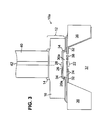
I. First Exemplary Embodiment - Configuration for Optical Modulation
In a first exemplary embodiment of an article according to the present invention
shown in FIG. 3, the fiber 40 is integrated with a micro device 10a operable to
modulate an optical signal. The fiber 40 is in optical communication with at least a
portion of a movable layer 20a. The movable layer 20a is supported at its periphery by
a support layer 36. A well 37, defined within the support layer 36, is located beneath
the movable layer 20a. In the illustrated embodiment, the bottom 38 of the well 37 is
defined by the movable layer 20a. The well 37 releases the movable layer 20a allowing
it move vertically. Additionally, the well 37 can be used for receiving a second optical
fiber, not shown, if the micro-device 10a is operated in a transmissive mode.
A nonmoving layer 26 is spaced from the movable layer 20a, creating a gap 30a
therebetween. Damping holes 24 are provided to control ringing in the movable layer
20a, especially at operating frequencies above about 1-2 MHz. In preferred
embodiments, the layer 20a has a circular shape.
Further description of design considerations for an optical modulator having a
circular shape and damping holes are provided in a U.S. Patent Application entitled
METHODS AND APPARATUS FOR AN IMPROVED MICROMECHANICAL
MODULATOR, filed February 1, 1996 as serial no. 08/565,453. Additional
description concerning the design of micromechanical optical modulators may be found
in U.S. Patent 5,500,761, and U.S. Patent Applications serial no. 08/478,590 filed June
7, 1995, serial no. 08/479,476 filed June 7, 1995 and serial no. 08/815,774. It should
be understood, moreover, that the micro-device 10a may suitably be structured, for
example, as a Fabry-Perot device having equal reflectivity mirrors. See, Aratani et al.,
"Process and Design Considerations for Surface Micromachined Beams for a Tuneable
Interferometer Array in Silicon," Proc. IEEE Micro. Electromech. Workshp., Ft.
Lauderdale, Fla, Feb. 7-10, 1993, pp. 230-235. The aforementioned patent, patent
applications and article, and any other such materials cited in this specification are
incorporated by reference herein. The modulators described in the aforementioned
patent and patent applications have a different structure than the aforedescribed
embodiment of the present invention. In view of the present teachings, those having
ordinary skill in the art will be able, as desired, to adapt the teachings of those
references to the presently disclosed device.
A voltage, delivered by a controlled voltage source, not shown, is applied to the
nonmoving layer 26 and the movable layer 20a. An electrostatic force is thereby
generated between those layers. The electrostatic force causes the movable layer 20a
to move from its quiescent or equilibrium position towards the nonmoving layer 26.
The change in position of the movable layer 20a results in a change in the size of the
gap 30a. As a result, the reflectivity of micro-device 10a changes. An optical signal
can be modulated by controlling the change in reflectivity via the controlled voltage
source.
It will be appreciated that the nonmoving layer 26 and the movable layer 20a
must be suitably conductive. If one or both of the layers 20a, 26 are not intrinsically
conductive, or not capable of being rendered conductive by doping with suitable
dopants, then an additional conductive layer is disposed adjacent to at least a portion of
one or both of the layers 20a, 26. Conductive layers 32 and 34 are shown disposed
adjacent to a portion of the respective movable and nonmoving layers. The conductive
layers may be, for example, aluminum, gold or other suitable metals, or polysilicon.
Using polysilicon as the material for the conductive layer 32 is convenient in the sense
that the support layer 36 may be polysilicon. In such a embodiment, the conductive
layer 32 can be formed by using a timed etch to prevent the etch from proceeding all
the way through the support layer during well 37 formation. A thin layer of the
support layer thus remains, serving as the conductive layer 32. As indicated above,
however, such an etch must be timed. Moreover, the optics expressions developed
herein do not allow for such a layer.
The movable and nonmoving layers must be optically transparent at the
operating wavelength(s). More particularly, region 22 of the movable layer 20a and
region 28 of the nonmoving layer 26, both in optical communication with the optical
fiber core 42, must be optically transparent. If one or both of the conductive layers 32,
34 are present, and such layers are not optically transparent at the relevant
wavelength(s), then such layers must not be present either below or above the regions
22 and 28 of the movable and nonmoving layers. The regions 22, 28 are referred to
herein as an optical window.
The micro-device 10 is fabricated using photolithographic methods. Briefly, a
first layer of silicon nitride or polysilicon is deposited on a first side of a silicon wafer.
That layer, when released, forms the movable layer 20a. A "pill" of a readily-etchable
sacrificial material, such as, without limitation, silicon dioxide, phosphoro-silicate glass
(PSG) or the like, is deposited on the first layer. A second layer, comprised of silicon
nitride or polysilicon, is deposited on top of the pill. The materials choice for the
second layer may be selected independently of the materials choice for the first layer. A
layer 16 of glass is deposited over the second layer. The wafer is etched from the
second side to the first layer. Holes 24 are etched into the first layer. Note that such
holes must be etched through the conductive layer 32, if present. Etchant is delivered,
through the holes 24, to the pill of sacrificial material sandwiched between the first and
the second layer. The sacrificial material is etched away, releasing the first layer. The
second layer is supported by the overlying layer 16 of glass. A layer 14 of cement, e.g.
epoxy, is used for attaching the fiber 40 to the layer 16.
An alternate embodiment of the integrating arrangement 12 for use with
suitably- structured micro-devices 10 does not require the layer 16 of glass. Such
suitably-structured micro-devices 10 incorporate a nonmoving layer 26 that is,
relatively speaking, thicker and/or of smaller diameter than the layer 26 present in
devices requiring the layer 16.
Additional information concerning the fabrication of micromechanical optical
modulators may be found in the above-referenced patent and patent applications.
The optical performance of the article as modulator shown in FIG. 3 and
described above can be characterized using expression [1]. Expression [1] was
developed based on the exemplary multi-layer article 4 shown in FIG. 1. The
exemplary article shown in FIG. 3 is related to the article 4 as follows: the fiber core
42 and the integrating arrangement correspond to layer a, the nonmoving layer 26
corresponds to the layer b, the gap 30a corresponds to the layer c, the movable layer
20a corresponds to the layer d, and the well 37 beneath the movable layer 20a
corresponds to the layer e.
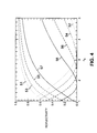
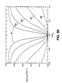
The optical performance of the first exemplary embodiment, as calculated using
expression [1], is shown in FIG. 4. That Figure shows reflectivity as a function of the
refractive index of the layer b, i.e., the nonmoving layer 26. Curves are shown for a
variety of values of the refractive index of layer d, i.e., the movable layer 20a. For
curves 51 and 52, nd = 3.0; for curves 53 and 54, nd = 2.5; for curves 55 and 56, nd =
2.0; and for curves 57 and 58, nd = 1.5. The curves are developed based on the
assumption that the refractive index of layer a, the optical core 42, is 1.467, which is a
typical value for single-mode fiber.
For curves 52, 54, 56 and 58, the thickness tc of the gap 30a is equal to mλ/
(4nc ), where m is an even integer and λ is the operating wavelength. Zero reflectivity is
observed for each of such curves at a particular value of the refractive index nb of the
layer b. For curves 51, 53, 55 and 57, the thickness tc of the gap 30a is equal to mλ/
(4nc) , where m is an odd integer. The curves 51, 53, 55 and 57 show a significantly
higher value of reflectivity at the same value of nb that resulted in zero reflectivity for
curves 52, 54, 56 and 58.
Contrast may be defined as the ratio of reflectivity at tc = mλ/ (4nc ) , where m is
an odd integer to the reflectivity at tc = mλ/(4nc ) where m is an even integer. FIG. 4
indicates that very high contrast is obtained if the refractive index nb of the nonmoving
layer 26 is an amount larger than the refractive index nd of the movable layer 20a. FIG.
4 shows, for example, that if nd = 2.0, which is the condition for curve 56, zero
reflectivity is obtained if nb is about 2.4. Both of those index values are in the
allowable range for silicon nitrate films. Such a film can be made to possess high
tensile stress, which is required for MHz-speed modulation devices.
In an exemplary design, the gap 30a is equal to 3λ/(4nc ) in the quiescent
position. Thus, there is a maxima in reflectivity at zero applied voltage. With an
applied voltage of the proper magnitude, the gap 30a spacing is reduced to about
2λ/(4nc ), which corresponds to zero reflectivity. As previously noted, the
aforedescribed embodiment of the present invention can be operated in either a
reflection mode with the single optical fiber 40, or in a transmissive mode wherein a
second fiber to receive the modulated signal that is transmitted, in varying amounts,
through the movable layer 20a. See, U.S. Patent Application 08/775,910 filed January
2, 1997.
II. Second Exemplary Embodiment - Configuration for Measuring Pressure
In a second exemplary embodiment of the present invention shown in FIG. 5,
the fiber 40 is integrated with a micro-device 10b configured for measuring pressure.
The micro-device 10b has a nonmoving layer 26 and a movable layer 20b, which layers
are spaced forming chamber 30b therebetween. The chamber 30b is analogous to the
gap 30a of the first exemplary embodiment. The movable layer 20b is supported at its
periphery by support layer 36. A well 37 is defined within the support layer 36
underneath the movable layer 20b. Fiber 40 is attached to the micro-device 10b by
integrating arrangement 12. As in the first exemplary embodiment, the integrating
arrangement preferably includes a layer 14 of cement and a layer 16 of glass. The layers
14 and 16 are index-matched to the fiber core 42.
The exemplary configuration for measuring pressure shown in FIG. 5 is
structurally similar to the configuration useful for optical signal modulation shown in
FIG. 3. There are, however, some structural differences arising from the functional
differences between those two configurations, as described below. For example, as
configured for measuring pressure, the movable layer 20b is actuated or moved from an
equilibrium position by the pressure exerted on it by a fluid in which the article is
immersed. As such, unlike the first configuration, the pressure measuring configuration
does not require any structure associated with applying a voltage to the movable and
non-moving layers.
Advantageously, and unlike prior art pressure measuring devices, the present
article, as configured for measuring pressure, is exceedingly small, e.g., as small as
about 25 microns, and more typically 100+ microns, so as to cause reduced
disturbances in the pressure-measuring environment. Moreover, the only connection to
the micro-device 10b incorporating the movable layer 20b is an optical fiber 40. This is
particularly advantageous in applications in which the present article is intended to be
placed well into a target environment, as opposed to being located along a vessel wall
or the like.
A second structural difference between the configuration for optical signal
modulation
and that for pressure measurement is that in the case of pressure measurement, there
are no damping holes 24 in the movable membrane 20b. In other words, the chamber
30b is sealed.
The operating principle underlying pressure measurement using the present
invention is described below. As the movable layer 20b is exposed to a fluid pressure,
it will move, i.e., bulge, towards the non-moving layer 26. The change in position of
the movable layer 20b results in a change in the size of the chamber 30b. As a result,
the reflectivity of micro device 10b changes. Such a change in reflectivity can be
correlated to the pressure extant on the movable layer 20b.
II.A Mechanical Response of an Article
According to the Present Invention
Configured for Measuring Pressure
The mechanical response of an article configured for measuring pressure
according to the present invention is described below. The chamber 30b is assumed to
have a cylindrical geometry for the following mathematical analysis. It should be
understood that such a geometry is not required. In cases where the geometry is not
cylindrical, the following analysis must be appropriately changed.
If the pressure Pd inside the chamber 30b is equal to the ambient pressure P, the
movable layer 20b is flat. The chamber 30b volume is then V o = πR 2 t o, where R is the
radius of the chamber 30b and to is its height. In a first embodiment, referred to herein
as a "type I pressure measuring device," the chamber 30b is assumed to be evacuated.
By definition, Pd is equal to zero for a type I pressure measuring device. In a second
embodiment, referred to herein as a "type II pressure measuring device," the chamber
30b is filled with a fixed amount of gas. For the type II pressure measuring device, the
pressure Pd inside the chamber 30b depends on the ambient temperature T and pressure
P, on the mechanical properties of the movable layer 20b, and on the amount of gas
sealed in the chamber 30b.
The equilibrium position of the membrane is determined the force equation:
[2] Etm /[12(1-σ2)] · ▿ 4 u(r) - ζ▿ 2 u(r) + f = 0
where: u(r) is the displacement of the movable layer 20b at radial distance r
from its center, tm is the thickness of the movable layer 20b, σ is Poisson's ratio, E is
Young's modulus, ζ is the stretching force per unit length along the edge of the
movable layer 20b, and f is an applied force per unit area.
For displacements u(r) that are small compared to the radius of the movable
layer 20b, membrane stress S is about constant and ζ = S tm. The expression for f is:
f = P - Pd - ρm g tm
where: ρm is the average density of movable layer 20b. Using typical numbers
for ρm and tm, e.g., ρm = 3.1 (silicon nitride) and tm = 0.2 microns (λ/4 membrane),
the quantity ρm g tm is found to be about 10-6 bar, and so will be neglected. The effect
of gravity as a contribution to the applied force f is therefore negligible. Thus, the
relative orientation of the movable layer, i.e., vertical, horizontal, etc., is not important.
In the following description, it will be assumed that the second term in
expression [2], which is proportional to the stress, is large compared to the first term
associated with bending moments. This applies if the stress S in the movable layer 20b
is greater than or equal to about 50 mega pascals (MPa).
The simplified force equation has the solution:
u(r) = [(P - Pd )(R 2 - r 2)]/(4S tm ).
The midpoint displacement ump , i.e., u(r = 0) is then given by:
ump = [R 2 /(4S tm )] · (P - Pd ).
A dimensionless parameter β is defined for use below:
β = [R 2 / (4S tm )] · (Po/2to ),
with P o defined as 1 bar. It should be understood that P o is simply a reference
parameter for use in developing the dimensionless parameter β. The expression for
midpoint displacement of the movable layer 20b may then be expressed:
[3] ump = 2β t o · (P - Pd ) / Po .
For a type I pressure measuring device, since Pd is defined to be equal to zero,
expression [3] becomes:
[4] ump = 2βt o · P/P o.
The movable layer 20b must not be allowed to contact the non-moving layer 26 over
the pressure range of the device, thus constraining the allowed values of β. If P max is
the maximum pressure to be measured, then for P < P max , ump < t o. Thus, using
expression [4]:
[5] β < ( P o / 2P max).
Thus, for example, a type I pressure device with a maximum pressure of 1 bar must
have β < 0.5.
For a type II pressure measuring device,
[6] (ump / to ) = {[1 + β (P/Pp )] - [(1- β (P/Pp ))2 + 4β (Po/Pp ) (T/Tp )]0.5 } /
(P/Po )
where: Pp is packaging pressure and Tp is the packaging temperature of the gas
in the chamber 30b at the time the chamber is sealed.
To simplify the following description, it will be assumed that Pp = 1 bar so that
Pp = P o and:
[7] (ump / to) = [1 + β (P/P o)] - [(1- β(P/P o))2 + 4β (T/Tp )]0.5
The movable layer 20b touches the non-moving layer 26 at P max. Setting (ump /
t o) = 1 at P max and T = Tp :
[8] Pmax/Po = 2 + 1/(2β).
Since β is positive, the right hand side of expression [8] is always greater than
2. As such, independent of the mechanical properties of the movable layer 20b, the
movable layer will not touch the non-moving layer 26 for pressures less than 2 bar.
That result is due to the compression of gas in the chamber 30b. That is, when the
movable layer 20b touches the non-moving layer 26, the volume of the chamber 30b
has been reduced by a factor of 2.
For Pmax/Po greater than 2, the requirement that the layers do not touch requires
that:
[9] β < 1/{2[(P max/P o)-2(T/Tp )]}.
For a high pressure gauge, i.e., P max /Po >> 1:
[10] β < P o/(2P max)
Note that expression [10] is the same as expression [5]. This result indicates that for
the stated conditions, compressing the gas in the chamber 30b generates a force that is
insignificant compared to the restoring force associated with the tension in the movable
layer 20b.
II.B Optical Response of an Article
According to the Present Invention
Configured for Measuring Pressure
The optical responses of type I and type II pressure measuring devices
according to the present invention are described below. As ambient pressure P
increases, the gap between movable layer 20b and the non-moving layer 26 decreases.
The gap size tc is given by:
[11] tc = to - ump
The midpoint displacement ump (P) is given by expression [4] for a type I
pressure measuring device and expressions [6] or [7] for a type II pressure measuring
device. Substituting tc (P) into expression [1] gives the amplitude of the reflected light
as a function of pressure.
FIGS. 6a, 6b and 7 show reflectivity versus P/Po ("the optical response")for a
type I pressure measurement device according to the present invention. For all
examples described in this Section, the pressuring measuring device is assumed to
measure the pressure of a fluid having an optical index of water, i.e., about 1.33.
FIG. 6a shows the optical response for a device with a chamber height t o = mλ
/(4nc), m = 2 and nb = nd = 2.00. As to the correspondence between the structure of
a pressure measuring device according to the present invention and the multi-layered
structure 4 shown in FIG. 1 and used in the development of expression [1], the fiber
core 42 and the integrating arrangement 12 correspond to layer a, the nonmoving layer
26 corresponds to the layer b, the chamber 30b corresponds to the layer c, the movable
layer 20b corresponds to the layer d, and the region 38 beneath the movable layer 20b
corresponds to the layer e.
The optical response shown in FIG. 6a is typical for a device in which the
nonmoving and movable layers are formed of silicon nitride, which has a refractive
index of about 2.0. In FIG. 6a, the curves numbered 60, 62, 64 and 66 show the
optical response for β = 0.5, 0.2, 0.1 and 0.05, respectively. All of the curves 60 - 66
begin at the origin since at P = 0, the movable layer is at its equilibrium position and t c
= to = λ / (2nc) implying zero reflectivity. As previously described, if β = 0.5, the
movable layer 20b touches the nonmoving layer 26 at P = 1bar. For a device operating
near 1 bar, β of 0.1 provides the highest sensitivity, i.e., the greatest change in
reflectivity for a given change in pressure, of the β values shown.
FIG. 6b shows the optical response for a device with the same chamber height
t o = mλ / (4nc ), m = 2, but nb = nd = 3.5. The refractive indices used for FIG. 6b are
typical for devices in which the nonmoving and movable layers are formed of
polysilicon. In FIG. 6b, the curves numbered 61, 63, 65 and 67 show the optical
response for β = 0.5, 0.2, 0.1 and 0.05, respectively. For a device operating near 1
bar, a β of 0.05 provides the highest sensitivity of the β values shown.
To achieve a higher sensitivity for operating near 1 bar ambient pressure, a
chamber 30b having a greater height to may suitably be used. Moreover, a device can
be designed to achieve a specific reflectivity at a particular ambient pressure by
appropriately adjusting chamber height to, as follows.
First, a desirable reflectivity Rsel is chosen from among the allowable range of
values for a given optical system. Due to the sinusoidal nature of the variation in
reflectivity with gap, the chosen value of Rsel occurs at many different values of t c.
Choosing to have device reflectivity increase with pressure, such different values of t c
are given by:
[12] tc = (m - α)λ/(4nc ),
with m being an even integer, and 0 ≤ α ≤ 1, where α is a modifier to integer
m. Combining expression [11] and [12] and using expression [4] with P equal to the
selected pressure Psel gives:
[13] t o = [(m - α)λ/(4nc )]/[1 - 2β Psel / Po ].
FIG. 7 shows the optical response of a type I pressure measuring device for
measuring pressures near 1 bar. Curves 70, 72, 74 are for β equals 0.2, 0.1 and 0.05,
respectively. The value of t o is determined from expression [13] with Psel = 1bar. Such
values are shown in TABLE 1. FIG. 7 is for the case where nb = nd = 2.0. The values
of to are calculated based on m = 2 and α = 1/3. FIG. 7 shows that sensitivity
increases with β. Sensitivity can be increased by increasing m to 4 or 6, etc.
If the product β
Psel is maintained constant,
to remains unchanged. Thus,
neglecting the rescaling of the abscissa and the β values, the optical response at another
pressure, for example,
Psel /
P o =10, would be identical to that at
Psel/Po = 1. See
TABLE 1.
| β @ Psel/Po = 1 | β @ Psel/Po = 10 | to /[λ(4nc )] | to , microns |
| 0.05 | 0.005 | 1.85 | 0.72 |
| 0.10 | 0.010 | 2.08 | 0.81 |
| 0.20 | 0.020 | 2.78 | 1.08 |
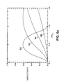
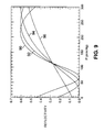
FIGS. 8a, 8b and 9 show the optical response for a type II pressure
measurement device according to the present invention. FIG. 8a and 8b show the
optical response for a device with a chamber height to = mλ / (4nc ), m = 4. For those
Figures, it is further assumed that the packaging pressure Pp = P o (= 1 atm) and the
packaging temperature Tp equals ambient temperature T. The midpoint displacement
ump (P) is thus given by expression [4] with T/TP = 1. FIG. 8a shows the optical
response for nb = nd = 2.00, i.e., silicon nitride-based movable layer 20b and
nonmoving layer 26 for a variety of β values. Curves 80, 82, 84, 86 and 88 show the
optical response for β equals 1.0, 0.5, 0.2, 0.1 and 0.05, respectively. FIG. 8b shows
the optical response for nb = nd = 2.00, i.e., polysilicon-based movable layer 20b and
nonmoving layer 26. Curves 81, 83, 85, 87 and 89 show, respectively, the optical
response for β equals 0.5, 0.2, 0.1, 0.05,and 0.02. In both Figures, at P/Po= 1,
movable layer 20b is flat so that the gap tc between the movable layer 20b and the
nonmoving layer 26 is equal to the chamber height t c. As such, reflectivity is zero.
As for a type I pressure measuring device, it is useful to set t o so that a
preselected reflectivity is obtained at a particular pressure Psel. Assuming packaging
pressure Pp equals P o (1 atm) and the temperature T equals the packaging temperature
Tp and combining expressions [6], [10] and [11] gives, for a type II pressuring
measuring device:
[14] to = [(m - α)λ/(4nc )]/{(-β Psel / P o) + [(1 - β Psel / P )2 + 4β]0.5}
One exemplary nonlimiting use of the present type II pressure measuring device
is for measuring blood pressure. The temperature control requirement is met by the
known and stable temperature of the human or other type of animal body into which
the device is inserted. For the present example, the device is assumed to function with
a midpoint pressure of 120 mm Hg. Thus,
Psel /
P o is equal to (760 + 120)/ 760 or
about 1.15. FIG 9 shows the optical response of such a device assuming
nb =
nd =
2.00,
m = 4 and α = 1/3. Curves 90, 92, 94 and 96 show the optical response for β
equals 2.0, 1.0, 0.5 and 0.2, respectively. Values of
t o calculated from expression [14]
are listed in TABLE 2.
| β | to/[λ/(4nc )] | t o, microns |
| 0.2 | 3.86 | 1.51 |
| 0.5 | 4.07 | 1.59 |
| 1.0 | 4.29 | 1.67 |
| 2.0 | 4.51 | 1.76 |
| 5.0 | 4.74 | 1.85 |
If the pressure measuring device is to useful over a range of about 50 to 300
mm Hg, then, with reference to FIG. 9, the device may be suitably constructed with a β
of 0.5. A variation in temperature of 1°C would change the pressure reading by about
0.3 percent.
In a further embodiment of an article configured for measuring pressure,
referred to herein as a type III pressure measurement device, the movable layer includes
a plurality holes of appropriate number and size. Thus, there will be gas on both sides
of the movable layer that is normally in equilibrium. If a change in pressure occurs in
the environment, and the frequency of that change is greater than 1/τ, where τ is a
characteristic time associated with the decay of pressure in the chamber, i.e., a
relaxation time, then a type III device can be used to indicate that change in pressure.
Thus, a type III pressure measurement device according to the present
invention can be used, for example, as a pressure surge indicator or microphone.
In the foregoing Figures, optical response was shown for a variety of values of
the dimensionless parameter β. The parameter β is a function of the several properties
of the movable layer 30b; in particular, its thickness, diameter and stress. The
parameter β was previously defined as:
β = [R 2 / (4S tm )] · (Po / 2to),
with P o defined as 1 bar. Expressing the stress S in MPa and substituting D/2 =
R, then:
[16] β = D 2 / (320S tm to).
Assuming, for the following illustrations, that nb = nd = 2.00 and λ = 1.56
microns, then the movable layer 30b has a thickness tm given by:
[17] tm = md λ/(4nd ) = 0.20md
with md = 1,3,5, ....
Representative values for the stress, thickness and diameter of the movable
layer 30b for some of the above-described exemplary embodiments of pressuring
measuring devices according to the present invention are provided below. The optical
response of a type I pressure measuring device was shown in FIG. 7. Selecting β =
0.2, Table 1 gives
t o = 1.08 microns. Those values of β and
t o, and expressions [16]
and [17] give:
D = 3.72 (md S)0.5.
Values of
D computed from the previous expression are listed in TABLE 3.
| S, MPa | md | D, microns |
| 150 | 1 | 46 |
| 150 | 3 | 80 |
| 150 | 5 | 102 |
| 600 | 1 | 92 |
| 600 | 3 | 160 |
| 600 | 5 | 204 |
| 1000 | 1 | 118 |
| 1000 | 3 | 204 |
| 1000 | 5 | 263 |
In preferred embodiments, the displacement of the movable layer 30b depends
linearly on the applied force. The stress due to displacement of the movable layer 30b
must therefore be small compared to the intrinsic stress of the layer. This requires that
ump be sufficiently small compared to D. The increase in stress in the movable layer 30b
is given by:
ΔS = (E/2)(πump/D)2.
Solving for D gives:
D ≈ 2.2 ump / [( S/E)(ΔS/S)]0.5
Using 3.85 x 10⁵ MPa for Young's modulus E of silicon nitride, and choosing ΔS/S <
0.1, then
D > 4300ump / S 0.5,
with S in MPa.
For the present example of a type I pressure measuring device with β = 0.2, the
device has a maximum usable pressure of about 1.3 bar. Using expression [4], the
midpoint displacement ump of the movable layer is about 0.6 microns. Thus, if S = 150
MPa, then
D ≥ 4300 · 0.6/(150)0.5 or about 200 microns. If S = 600 MPa, then D ≥ 100 microns
and if S = 1000 MPa, then D ≥ 80 microns.
Similar calculations can be performed for a type I pressure measuring device
with Psel = 10 bar. Taking β = 0.02, TABLE 1 gives t o = 1.08 microns. Those values
of β and to, and expressions [16] and [17] give D = 1.18 (md S)0.5. Likewise, for a
type II pressure measuring device with Psel = 120 mm of Hg and selecting β = 0.02,
TABLE 2 gives t o = 1.59 microns. Those values of β and to, and expressions [16] and
[17] give D = 7.13 (md S)0.5.
The movable layer 20b of type I and II pressure measuring devices do not have
damping holes, such as the damping holes 24 of the movable layer 20a of the article
configured for optical modulation. As such, a fabrication method different from that
described for the optical modulation configuration is required. Such a method is
described below.
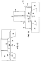
FIG. 10 shows a side view of an arrangement of various material layers that can
be used in fabricating pressure measuring devices according to the present invention.
Layers shown in FIG. 10 include the support layer 360, typically silicon or polysilicon.
A layer 200, a part of which forms the movable layer 20b after release, is deposited on
the support layer 360. A sacrificial layer is deposited on a portion of the layer 200.
The sacrificial layer is deposited to a thickness equivalent to the height t o of the
chamber 30b. The sacrificial layer is patterned, typically photolithographically, to form
a central "pill" 301 of material having four "arms" 303 depending therefrom, as shown
in FIG. 11. As described in more detail below, the arms 303 are etched away to form
access ways or channels for delivering etchant to the pill 301.
The shape of the pill 301 defines the shape of the movable layer 20b. In
preferred embodiments, the pill 301 is circularly-shaped to define a circular movable
layer 20b. It will be appreciated that while four arms 303 are shown in FIG. 11, more
or less of such arms may suitably be used for providing access channels to the pill 301.
For simplicity, the pill 301 and arms 303 are shown in FIG. 10 as a sacrificial region
305.
With continuing reference to FIG. 10, a layer 260, a part of which forms the
nonmoving layer 26b after release, is deposited over the arms 303, the pill 301 and
exposed regions of the layer 200. A layer 16 of glass, e.g., silicon oxide, which was
mentioned previously in conjunction with a description of the integrating arrangement
12, is deposited on top of the layer 260. Preferably, the layer 16 is in the range of from
about 10 to 15 microns in thickness, though greater or less thicknesses may suitably be
used. The layers 200 and 260 can be formed from materials such as, without limitation,
silicon oxide, polysilicon, or, more preferably, silicon nitride.
Access wells 307, one for each arm 303, are formed through the layer 16 and
the layer 260 to communicate with the arms 303. The access wells 307 can be formed
by etching with an appropriate wet or dry etch. An exemplary wet etch suitable for
etching the layers include HF-based solutions, and exemplary dry etches include
fluorine-containing gasses, such as, for example, sulfur hexafluoride and
carbontetrafluoride. The access wells are preferably about 3 to 10 microns in diameter.
In an alternative embodiment, the arms 303 can be accessed from the side rather than
from above.
The chamber 30b is formed by removing the pill 301. To do so, etchant is
delivered through the access wells 307 to the arms 303. Since the arms 303 and pill
301 are formed of a material that etches rapidly compared with the surrounding
material, e.g., silicon nitride, silicon oxide and the like, the arms 303 form channels in
the surrounding material as they are etched. The arms 303 may suitably be patterned to
have a width of about 5 to 10 microns and a height equivalent to the height of the pill
301. After the arms 303 are completely removed by the etchant, the channels formed
thereby lead to the pill 301. Etchant is delivered through the channels to the pill 301,
which is selectively etched in preference to the surrounding material layers 200, 260.
In preferred embodiments, the support layer 360, the pill 301 and the arms 303,
are polysilicon and the movable layer 20b is silicon nitride. Using polysilicon for both
of those layers advantageously facilitates etching them at the same time. Etchants
useful for removing polysilicon include potassium hydroxide, ethylene diamine
pyrocatechol (EDP) and hydrazine. Moreover, the aforementioned polysilicon etchants
etch polysilicon at a much faster rate than either silicon nitride or silicon oxide. Thus,
the etch to remove the pill 301 does not require careful timing. Furthermore, the layer
16, which is typically silicon oxide, can be deposited before removing the pill 301.
Depositing the layer 16 after removing the pill 301 is problematic. In less preferred
embodiments, PSG can be used for the sacrificial layer, which can be etched using
hydrofluoric acid. After removing the pill 301, the access wells 307 may be filled with
an epoxy. Alternatively, glass can be sputter deposited over the micro-device.
The well 37 is required, in conjunction with the gap 30b, for forming the
movable layer 20b. Etchant suitable for etching the support layer 360 is selected as a
function of the material used for the support layer. Such selection is within the
capabilities of those ordinarily skilled in the art. FIG. 12 shows the micro-device 10b
after gap and well formation.
III. Third Exemplary Embodiment - Configuration for Measuring
Temperature
In a third exemplary embodiment of the present invention shown in FIG. 13, the
fiber 40 is integrated with a micro-device 10c configured for measuring temperature.
The micro-device 10c has a nonmoving layer 26 and a movable layer 20c, which layers
are spaced forming chamber 30c therebetween. The movable layer- 20b is supported at
its periphery by support layer 36. Fiber 40 is attached to the micro-device 10c by
integrating arrangement 12. As in the first and second exemplary embodiments, the
integrating arrangement preferably includes a layer 14 of cement and a layer 16 of
glass. The layers 14 and 16 are index-matched to that fiber core 42, i.e., the layers and
the core have the same index of refraction.
A cavity 33 is formed within the support layer 36 beneath the movable layer
20c. The cavity 33 is evacuated. The cavity 33 isolates the chamber 30c from
variations in the ambient pressure. The movable layer 30c moves only in response to
temperature changes that alter the pressure in the gas-filled chamber 30c. The change
in position of the movable layer 20c results in a change in the size of the chamber 30c.
As a result, the reflectivity of micro device 10c changes. Such a change in reflectivity
can be correlated to the ambient temperature T.
In the description that follows, it is assumed that the chamber 30c is sealed with
gas at packaging pressure Tp packaging pressure Pp , and then cavity 33 is evacuated.
Due to the pressure differential, the movable layer 30c bulges towards the cavity 33.
The cavity 33, which corresponds to the "e" layer shown in FIG. 1, has an optical index
of 1.
The midpoint deflection of the movable layer 30c can be determined using
expression [7], and with ambient pressure P defined as zero:
[15] (ump / to ) = {[1 - [1 + 4β (Po/Pp) (T/Tp )]0.5} / (Po / Pp).
The midpoint deflection ump is always less than zero since the movable layer
20c deflects downwardly. As such, the movable layer 30c will never contact the
nonmoving layer 26. If the packaging pressure Pp is equal to P o, then expression [15]
may be written:
[16] (ump / to ) = 1 - [1 + 4β(T/Tp)]0.5.
Using expression [17] below, a device according to the present invention can be
designed to provide a preselected reflectivity for a given temperature Tsel .:
[17] t o = [(m + α)λ/(4nc )]/(1 + 4βTsel / Tp )0.5
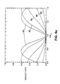
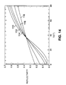
FIG. 14 shows the optical response, i.e., reflectivity vs. temperature, for a
temperature measuring device with Tsel = 310 K (37°C), nb = nd = 2.00, Tp = 300 K,
m = 6 and α = 1/3.
Chamber height t o for a variety of values of β are shown in TABLE 4. Expression [17]
was used to calculate t o and expressions [1], [11] and [16] were used to generate the
optical response curves shown in FIG. 14. Curves 110, 112, 114, 116 and 118 show
the optical response for β equals 0.1, 0.2, 0.5, 1.0 and 10.0, respectively
FIG. 15 shows the optical response for a temperature measuring device with
Tsel
= 473 K (200C),
nb =
nd = 2.00,
Tp = 300 K,
m = 4 and α = 1/3. Values for chamber
height
t o are listed in TABLE 5. Curves 120, 122, 124, 126 and 128 show the optical
response for β equals 1.0, 0.5, 0.2, 0.1 and 0.05, respectively.
| β | to /[λ/(4nc )] | t o, microns |
| 0.1 | 5.33 | 2.08 |
| 0.1 | 4.69 | 1.83 |
| 0.5 | 3.62 | 1.41 |
| 1.0 | 2.80 | 1.09 |
| 10.0 | 0.97 | 0.38 |
| β | to/[λ/(4nc )] | to, microns |
| 0.05 | 3.78 | 1.47 |
| 0.10 | 3.39 | 1.32 |
| 0.20 | 2.88 | 1.12 |
| 0.50 | 2.13 | 0.83 |
| 1.00 | 1.60 | 0.63 |
Representative values for the stress, thickness and diameter of the movable
layer 30b for some of the above-described exemplary embodiments of temperature
measuring devices according to the present invention are provided below. The optical
response of a temperature measuring device with
Tsel = 300 K was shown in FIG. 14.
Selecting β = 1.0, Table 4 gives
t o = 1.09 microns. Those values of β and
t o, and
expressions [16] and [17] give:
D = 8.35 (md S)0.5.
Values of
D computed from the previous expression are listed in TABLE 6 below.
| S, MPa | md | D, microns |
| 150 | 1 | 102 |
| 150 | 3 | 177 |
| 150 | 5 | 228 |
| 600 | 1 | 205 |
| 600 | 3 | 354 |
| 600 | 5 | 457 |
| 1000 | 1 | 264 |
| 1000 | 3 | 457 |
| 1000 | 5 | 590 |
Likewise, with (Tsel = 473K and selecting β = 0.5, TABLE 5 gives t o = 0.83
microns. Those values of β and to, and expressions [16] and [17] give D = 5.15 (md
S)0.5.
A temperature measuring device according to the present invention can be
formed using a method very similar to that used for fabricating the present type I and II
pressure measuring devices. For the temperature measuring device, the fabrication
method must be modified to provide the cavity 33. This may be simply accomplished
by forming the well 37 as described in previous embodiments and then "capping" it,
such as by bonding a silicon wafer over the mouth of the well.
The devices described in Sections I - III above can be advantageously formed
into arrays. Such arrays can be used, for example, to provide a pressure or temperature
profile of a very localized phenomenon. In one exemplary embodiment, a plurality of
pressure or temperature measuring devices are fabricated on a wafer. One or more of
such wafers are formed and embedded in, or disposed on, a surface exposed to the
environment to be measured. An optical signal reflected from the movable layer (or
transmitted through it for transmissive device) of each device is guided by the optical
fiber to a photodetector array. The photodetector array is operable to measure the
optical signal delivered from each optical fiber. An electrical signal corresponding to
measured optical signal is produced by the photodetector array and delivered to a
processor operable to convert the signal information to a temperature or pressure using
data developed according to the present invention.
In a second exemplary embodiment, at least one pressure measurement device
and one temperature measurement device according to the present invention are
fabricated in close proximity to one another on a single chip. Such an arrangement
provides the ability to measure the temperature and pressure of an environment at
nearly the same location. Fabrication of wafers possessing more than one type of
measurement device can be accomplished by cofabrication or by using flip-chip bonding
methods, which are generally well known. For a description of a flip-chip bonding
method for forming chips containing more than one type of device, see U.S. Patent
Application 08/766,214 filed December 12, 1996 and entitled HYBRID CHIP AND
METHOD THEREFOR.
Although specific embodiments of this invention have been shown and
described herein, it is to be understood that these embodiments are merely illustrative
of the many possible specific arrangements that can be devised in application of the
principles of the invention. Numerous and varied other arrangements can be devised in
accordance with these principles by those of ordinary skill in the art without departing
from the scope and spirit of the invention.