EP0889682A2 - Power bus system in a tower building block system - Google Patents
Power bus system in a tower building block system Download PDFInfo
- Publication number
- EP0889682A2 EP0889682A2 EP98110944A EP98110944A EP0889682A2 EP 0889682 A2 EP0889682 A2 EP 0889682A2 EP 98110944 A EP98110944 A EP 98110944A EP 98110944 A EP98110944 A EP 98110944A EP 0889682 A2 EP0889682 A2 EP 0889682A2
- Authority
- EP
- European Patent Office
- Prior art keywords
- printed circuit
- modular
- block
- blocks
- power
- Prior art date
- Legal status (The legal status is an assumption and is not a legal conclusion. Google has not performed a legal analysis and makes no representation as to the accuracy of the status listed.)
- Withdrawn
Links
- 239000004020 conductor Substances 0.000 description 11
- IOPBNBSKOPJKEG-UHFFFAOYSA-N 1,2-dichloro-3-(3,5-dichlorophenyl)benzene Chemical group ClC1=CC(Cl)=CC(C=2C(=C(Cl)C=CC=2)Cl)=C1 IOPBNBSKOPJKEG-UHFFFAOYSA-N 0.000 description 5
- 230000013011 mating Effects 0.000 description 5
- 230000008901 benefit Effects 0.000 description 3
- 230000007935 neutral effect Effects 0.000 description 3
- 239000002537 cosmetic Substances 0.000 description 2
- 238000010586 diagram Methods 0.000 description 2
- 150000003071 polychlorinated biphenyls Chemical class 0.000 description 2
- 230000004075 alteration Effects 0.000 description 1
- 230000008859 change Effects 0.000 description 1
- 230000008878 coupling Effects 0.000 description 1
- 238000010168 coupling process Methods 0.000 description 1
- 238000005859 coupling reaction Methods 0.000 description 1
- 238000002955 isolation Methods 0.000 description 1
- 230000007246 mechanism Effects 0.000 description 1
- 238000000034 method Methods 0.000 description 1
- 230000004048 modification Effects 0.000 description 1
- 238000012986 modification Methods 0.000 description 1
- 230000000717 retained effect Effects 0.000 description 1
- 125000006850 spacer group Chemical group 0.000 description 1
- 239000002699 waste material Substances 0.000 description 1
Images


Classifications
-
- G—PHYSICS
- G06—COMPUTING; CALCULATING OR COUNTING
- G06F—ELECTRIC DIGITAL DATA PROCESSING
- G06F1/00—Details not covered by groups G06F3/00 - G06F13/00 and G06F21/00
- G06F1/16—Constructional details or arrangements
- G06F1/18—Packaging or power distribution
- G06F1/189—Power distribution
Definitions
- This invention relates to a power bus in a tower containing computing system devices. More particularly, this invention relates to the design of such a bus as integrated into building blocks used to build the tower.
- Modular towers for storing computing system devices offer the advantage of providing only exactly the amount of space required to contain the computing system devices. As more devices are added, a module of the tower is added to accommodate the additional device.
- a modular tower system provides the ability to adjust the physical size of the computing system to the amount of space required to store the computing system devices. What is needed is a solution to the above problems of powering the computing system devices.
- the invention in its broad form, resides in an apparatus to incorporate a power bus in a modular electronic building block system as recited in claim 1.
- a modular tower system containing computing system devices have been solved by incorporating the power bus into the modules of the tower system.
- the power bus is incorporated into modular blocks of the building block system by using a printed circuit element to carry the power bus in each modular block.
- the printed circuit element is mounted and positioned in each module to electrically connect with a printed circuit element in a next adjacent modular block when two modular blocks are positioned adjacent to each other.
- the printed circuit element is precisely located in each modular block at a predetermined position relative to alignment positioning elements in the modular block.
- Positioning elements provide alignment between adjacent modular blocks to precisely position one modular block adjacent the other modular block. This aligns the printed circuit elements of the adjacent blocks for connection from the printed circuit element in one modular block to the printed circuit element in the other modular block.
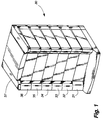
- FIG. 1 shows a tower assembly 30 of electronic modules composed of a base unit 31, five tower building block units 32-36, and a cap unit 37. Each of these units is covered by a cosmetic panel and the details of their structure hidden by those panels is discussed in greater detail below. Also, as is evident from the description presented in the copending application referenced above, the assembly 30 could include a greater or lesser number of block units similar to 32-36.
- FIG. 2 presents an arrangement 50 of three racks 51, 52 and 53 either free standing or attached to each other.
- Racks 51 and 53 are composed of ten block units in addition to their base and cap units whereas rack 53 is composed of nine block units plus the base and cap units.
- Cap units 13 and 51-53 typically include latch elements to mate with the blocks of each column and lock them in place relative to one another.
- these caps are not absolutely necessary under all circumstances. For instance, if the electronic module attached between tower block units is adequately secure to provide a cross-bracing function, such separate caps can be omitted, although use of connector covers or even cosmetic cover panels on the topmost block pair could complete EMI isolation and/or could prevent fouling of the electrical connectors or the interior of either column of blocks.
- Rack 53 includes a double sized block element 55 which is supported by four tower building blocks 56A, 56B, 56C and 56D. Such a procedure allows use of common sized tower building blocks. However, those having normal skill in the art will recognize that single tower building blocks could replace blocks 56A and 56B, as well as a single block for 56C and 56D but with those single blocks twice the size of each of blocks shown.
- the modularized power bus in the preferred embodiment is placed on a Printed Circuit Board (PCB).
- PCB Printed Circuit Board
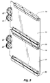
- Two printed circuit boards 10 and 12 are shown in FIG. 3. Each printed circuit board has a female connector at the top and a male connector at the bottom. The male connector has a shroud mounted around the pins, and therefore the pins are not visible in FIG. 3.
- Female connector 14 pin receptacles also not shown
- male connector 16 is at the bottom of printed circuit board 10.
- female connector 18 is at the top of printed circuit board 12
- male connector 20 is at the bottom of printed circuit board 12.
- Printed circuit board 10 is connected to printed circuit board 12 through male connector 16 and female connector 18.
- Each Printed Circuit Board is mounted in a module or building block of the tower building block system. Accordingly, when the building blocks are connected together, the connectors mate as shown in FIG. 3 between connectors 16 and 18. The alignment for obtaining proper mating of the connectors will be described hereinafter.
- the connectors used with the PCB in the particular example shown are not self-aligning connectors. Instead, the PCBs are precisely mounted in the building blocks and building blocks themselves have guide pins and receiving holes. These guide pins and receiving holes guide the tower building blocks into place and, at the same time, guide the mating of the connectors for the PCBs mounted in the building blocks. Double connectors, male and female, have been shown. Alternatively, other arrangements such as printed circuit board edge connectors could be used as shown in FIGS. 7A and 7B described hereinafter.
- Power outlets 22 and 24 on board 10 are connected to provide one phase of power from each of two power busses on board 10.
- power outlets 23 and 25 on board 10 are connected to provide one phase of power from each of two power busses on board 12.
- the tower building block system has two columns, or towers, with a shelf of computing system devices mounted between blocks at the same level between the two columns.
- the input/output bus printed circuit boards In the building blocks of one tower, are mounted the input/output bus printed circuit boards.
- the power bus printed circuit boards In the building blocks of the second tower, are mounted the power bus printed circuit boards.
- FIG. 4 is a somewhat generalized layout diagram for a printed circuit board along the lines of board 10 or 12 in FIG. 3 or board 58 in FIG. 7A.
- the board base 65 has a series of electrical conductors formed thereon as shown and also on the reverse side of the board for the purpose of effecting the electrical connections schematically illustrated in FIG. 5.
- the conductors of FIG. 4 include ground connections 66A, 66B and 66C while the primary power source neutral is connected to conductor 67A and the secondary power source neutral is connected at 67B.
- the three phases of the primary power are connected to conductor strips 71A, 71 B and 71C while the secondary three phases of power are connected to 72A, 72B and 72C.
- the conductors are likewise connected to the equipment module retained by the associated block through an IEC connector as at 70A and 70B.
- the power connections for the phase attached to the unit is transferred to the IEC connector on the reverse side of base 65 and as shown in FIG. 5.
- power from another phase or power from all three phases of either or both power sources can energize the equipment module through appropriate IEC connections and etched conductors.
- shorting of all three phase lines and introduction of a single phase power source is possible especially through the base unit in which case it is possible to employ the conductors as shown in both FIG. 4 and FIG. 5 without modification.
- FIG. 5 illustrates connection of power from phase A of both power sources to IEC connector contacts 70A and 70B.
- the reverse side of board 65 would include a conductor for coupling the neutral line of the secondary power source to the IEC connector 70B.
- the board 65 reverse side conductors likewise shift each of the three phases of both the primary and secondary power sources by one place at the output connections 73 and 74 for the next block as compared to the input connections 71 and 72. That is, the first phase at 71A is actually coupled to an output terminal via conductor strip 73A while 71B and 71C are respectively shifted into conductors 73B and 73C as shown. This facilitates automatic distribution of the loads presented by the equipment modules amongst the various phases of the different power sources.
- the board of FIG. 4 is often set up to couple a single phase of power to the equipment module held in place by the particular block retaining board 65. In many circumstances, a single phase of power is all that the equipment module demands. Typically, these modules are contemporary disk drives, tape drives, data processors, controllers, and the like.
- FIG. 6 shows one tower building block with an upper latch element and a lower latch element to fasten the building block to the next higher or lower block respectively.
- the building block is made up of walls 41 and 42 which are shown exploded apart in FIG. 6.
- Lower latch element 43 is shown fastened to wall 42.
- Upper latch element 44 is shown above wall 42.
- latch elements 43 or 44 is normally secured in place and a power bus printed circuit board is fastened to wall 42 at a precise location in the building block.
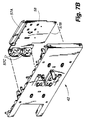
- FIG. 7A shows a power bus printed circuit board 58 exploded away from wall 42 of the building block.
- Printed circuit board 58 is attached to posts 60 molded into wall 42.
- Printed circuit board 58 is using a board edge type of electrical connector 59.
- Posts 60 have small registration posts 61 or pins at their tops that engage holes 62 in printed circuit board 58.
- the registration posts 61 snap into holes 62, or alternatively serve to register the position of PCB 58 in place until wall 41 snaps into wall 42.
- wall 41 has spacers to hold PCB 58 on posts 60 when the walls snap together.
- posts 60 with registration posts 61 engaging holes 62 serve to precisely locate PCB 58 relative to alignment posts and alignment receivers on the walls 41 and 42 of the building block.
- FIG. 7B wall 42 and PCB 58 are shown as viewed from the other side of wall 42 as shown in FIG. 7A.
- Power bus PCB 58 uses an edge connector 57A (slot in top of connector to engage edge of next board not shown).
- Edge 57B has printed circuit pads to engage and electrically connect the power bus on the board to edge connector on the next lower power PCB.
- Power outlets 57C are the power connectors for providing power to computing system devices mounted on the shelf that will be fastened to wall 42 of the tower building block.
- wall 41 of the building block has alignment posts or pins 46A, 46B and 46C at the bottom of wall 41.
- the top of wall 41 has alignment receiving holes 47A and 47C and receiving slot 47B.
- Similar alignment posts and alignment receivers are on wall 42. However, the alignment posts are at the top of wall 42, and the alignment receivers are at the bottom of wall 42. Only alignment posts 48 are visible for wall 42.
- alignment posts 46 of wall 41 in the upper block engage alignment receivers 47 in the lower block.
- alignment pins 48 of wall 42 in the lower block engage alignment receivers in the upper block. In this way, two blocks are physically mated.
- the alignment posts and alignment receivers either or both, have tapered surfaces to assist the initial alignment and mating of the posts in the receivers.
- the edge connector 57A of board 58 in the lower building block will be properly aligned with the edge 57B of the board 58 in the upper building block.
- the electrical connection elements also are aligned and mated so that the electrical connection between boards is made. If male and female connectors are used as in FIG. 3, the male connector is at the bottom of board 58 and the female connector is at the top of board 58. The connectors are guided into alignment by alignment posts and alignment receivers on the walls of the building blocks.
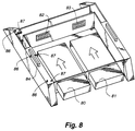
- the base 85 of the tower building block system is shown with power entry units 80 and 81.
- the power entry unit 80 provides the three phase power for one of the power buses and power entry unit 81 provides the three phase power for the other power bus.
- Each power entry unit 80 and 81 has a connector (not visible) on the back of the power entry unit that mates with connector 82 and 83, respectively.
- Conventional power cables (not shown) connect connectors 82 and 83 to power bus connector 84.
- Power bus connector 84 mates with the power bus connection on the power bus PCB in the lower most building block when the building block is stacked and latched onto the base 85.
- Alignment pins 86 and alignment receivers 87 are provided on base 85 to guide the mating of a building block to the base.
- Connector 84 is located relative to the alignment pins 86 and alignment pin receiving holes 87 so that when the building block stacks on the base, the power connection pads, or male connector, at the edge of the power bus PCB in the building block mate with edge connector 84.
- the alignment pins 86 and alignment receiving holes 87 are schematically shown in FIG. 8. This alignment and mating structure is embodied and functions in the same manner as described above in reference to FIG. 6.
Abstract
Description
- FIG. 1 is an overall isometric view of an environment of a prefered emboiment of the present invention and includes a tower composed of a base unit, five shelf units and a cap unit.
- FIG. 2 is an overall isometric view of three towers with ten modules on the outer towers and a double shelf unit in the middle tower.
- FIG. 3 shows two printed circuit boards interconnected to implement a preferred embodiment of the invention where power buses are passed up the tower building block system.
- FIG. 4 is a layout view of a printed circuit board having a pair of three phase AC power connections arrayed thereon.
- FIG. 5 is a simplified circuit diagram of the three phase connections associated with the printed circuit board of FIG. 4.
- FIG. 6 shows alignment pins and receivers in a tower building block into which a power bus printed circuit board is mounted.
- FIG. 7A shows a printed circuit board and posts on one wall of the building block for precisely locating the power bus printed circuit board.
- FIG. 7B shows the printed circuit board and wall of
FIG. 7A from the reverse side of the wall and
illustrates the power bus outlets on printed
circuit board 58. - FIG. 8 shows the base of the tower building block system with the power entry units and connectors in the base.
Claims (3)
- In a modular building block system for containing computing system devices, apparatus for incorporating a power bus in modular blocks of the building block system, said apparatus comprising:a printed circuit element carrying the power bus mounted in each modular block;said printed circuit being element positioned in each modular block to electrically connect with a printed circuit element in a next adjacent modular block when two modular blocks are positioned adjacent to each other.
- The apparatus of claim 1, wherein there are a plurality of power buses on the printed circuit elements and only one power bus is distributed from each modular block.
- The apparatus of claim 1 wherein:said printed circuit element is precisely located in each modular block at a predetermined position; andpositioning elements providing alignment between adjacent modular blocks to precisely position one modular block adjacent the other modular block and thereby connect a printed circuit element in said one modular block to the printed circuit element in the other modular block.
Applications Claiming Priority (2)
| Application Number | Priority Date | Filing Date | Title |
|---|---|---|---|
| US884938 | 1997-06-30 | ||
| US08/884,938 US5966292A (en) | 1997-06-30 | 1997-06-30 | Power bus system in a tower building block system |
Publications (2)
| Publication Number | Publication Date |
|---|---|
| EP0889682A2 true EP0889682A2 (en) | 1999-01-07 |
| EP0889682A3 EP0889682A3 (en) | 1999-09-08 |
Family
ID=25385767
Family Applications (1)
| Application Number | Title | Priority Date | Filing Date |
|---|---|---|---|
| EP98110944A Withdrawn EP0889682A3 (en) | 1997-06-30 | 1998-06-15 | Power bus system in a tower building block system |
Country Status (3)
| Country | Link |
|---|---|
| US (1) | US5966292A (en) |
| EP (1) | EP0889682A3 (en) |
| JP (1) | JPH11175195A (en) |
Cited By (1)
| Publication number | Priority date | Publication date | Assignee | Title |
|---|---|---|---|---|
| WO2001015499A1 (en) * | 1999-07-23 | 2001-03-01 | Walter Roland Chen | Parallel expansion local bus interface card-type i, ii & iii |
Families Citing this family (10)
| Publication number | Priority date | Publication date | Assignee | Title |
|---|---|---|---|---|
| US6469901B1 (en) * | 2000-05-15 | 2002-10-22 | 3C Interactive, Inc. | System and method for cartridge-based, geometry-variant scalable electronic systems |
| WO2003035484A2 (en) * | 2001-10-23 | 2003-05-01 | Norse Dairy Systems, Inc. | Sleeve for conical food product and process for producing the sleeve |
| US8107244B2 (en) | 2008-12-22 | 2012-01-31 | National Instruments Corporation | Connecting a plurality of chassis using a rigid connection |
| US9220180B2 (en) * | 2010-12-09 | 2015-12-22 | Richard Anthony Dunn, JR. | System and methods for scalable parallel data processing and process control |
| US8576570B2 (en) | 2011-03-21 | 2013-11-05 | NCS Technologies, Inc. | Adaptive computing system with modular control, switching, and power supply architecture |
| US8964396B1 (en) * | 2012-04-11 | 2015-02-24 | Google Inc. | Rack power and data bus |
| CN103979089B (en) * | 2014-05-21 | 2017-11-21 | 哈尔滨工程大学 | A kind of underwater robot electronic compartment of stack assembling structure |
| TWI566083B (en) * | 2015-04-24 | 2017-01-11 | 台達電子工業股份有限公司 | Standalone Uninterruptible Power Supply |
| US11177618B1 (en) * | 2020-05-14 | 2021-11-16 | Dell Products L.P. | Server blind-mate power and signal connector dock |
| US11749922B2 (en) | 2020-09-01 | 2023-09-05 | Ge Infrastructure Technology Llc | Dual-sided connector for printed circuit board |
Citations (5)
| Publication number | Priority date | Publication date | Assignee | Title |
|---|---|---|---|---|
| DE7113834U (en) * | 1971-04-10 | 1971-07-01 | Kolbe H & Co | Holder for several electrical device units lined up next to one another |
| US4477862A (en) * | 1982-05-19 | 1984-10-16 | Gould Inc. | Backplane connector |
| DE9104384U1 (en) * | 1991-04-10 | 1991-06-06 | Siemens Ag, 8000 Muenchen, De | |
| GB2271446A (en) * | 1992-04-29 | 1994-04-13 | Hany Neoman | User-built and upgradable personal computer |
| US5604662A (en) * | 1992-08-20 | 1997-02-18 | Streamlogic Corporation | Expandable modular data storage system |
Family Cites Families (1)
| Publication number | Priority date | Publication date | Assignee | Title |
|---|---|---|---|---|
| US4401351A (en) * | 1981-09-28 | 1983-08-30 | Advant Corporation | Expandable card cage |
-
1997
- 1997-06-30 US US08/884,938 patent/US5966292A/en not_active Expired - Lifetime
-
1998
- 1998-06-15 EP EP98110944A patent/EP0889682A3/en not_active Withdrawn
- 1998-06-30 JP JP10184880A patent/JPH11175195A/en active Pending
Patent Citations (5)
| Publication number | Priority date | Publication date | Assignee | Title |
|---|---|---|---|---|
| DE7113834U (en) * | 1971-04-10 | 1971-07-01 | Kolbe H & Co | Holder for several electrical device units lined up next to one another |
| US4477862A (en) * | 1982-05-19 | 1984-10-16 | Gould Inc. | Backplane connector |
| DE9104384U1 (en) * | 1991-04-10 | 1991-06-06 | Siemens Ag, 8000 Muenchen, De | |
| GB2271446A (en) * | 1992-04-29 | 1994-04-13 | Hany Neoman | User-built and upgradable personal computer |
| US5604662A (en) * | 1992-08-20 | 1997-02-18 | Streamlogic Corporation | Expandable modular data storage system |
Cited By (1)
| Publication number | Priority date | Publication date | Assignee | Title |
|---|---|---|---|---|
| WO2001015499A1 (en) * | 1999-07-23 | 2001-03-01 | Walter Roland Chen | Parallel expansion local bus interface card-type i, ii & iii |
Also Published As
| Publication number | Publication date |
|---|---|
| JPH11175195A (en) | 1999-07-02 |
| EP0889682A3 (en) | 1999-09-08 |
| US5966292A (en) | 1999-10-12 |
Similar Documents
| Publication | Publication Date | Title |
|---|---|---|
| US6075704A (en) | Input/output bus system in a tower building block system | |
| US8475177B2 (en) | Backplane cable interconnection | |
| US4703394A (en) | System for interconnecting orthogonally disposed printed circuit boards and switching networks employing same | |
| US5966292A (en) | Power bus system in a tower building block system | |
| EP1835794A2 (en) | Modular UPS systems and methods using modular interconnect assemblies | |
| US20050032398A1 (en) | Interconnecting module for the base of electronic equipment casing | |
| EP3301763B1 (en) | Electronic device | |
| CA1287927C (en) | Printed circuit board mounting for communication termination | |
| EP0421960B1 (en) | Function unit for electronic equipment | |
| RU2422959C2 (en) | Magazine for power supply components, power supply components, unit of power supply components and methods of assembly | |
| EP0416771B1 (en) | Circuit assembly | |
| US6317348B1 (en) | UPS chassis design having an internal support structure | |
| JP4332557B2 (en) | Interface extensions for modular platform applications | |
| JPH1197815A (en) | Device for connecting printed wiring board of another product | |
| US20010027066A1 (en) | Modular power connector system | |
| US5446621A (en) | Platform module system for a larger electronic system | |
| EP0387011A2 (en) | Modular computer and interface system | |
| US5748430A (en) | Integrated hybrid surge protector architecture configured to accomodate multiple replaceable communication signal surge protection modules in common housing with AC voltage receptacle terminal strip | |
| US20090053919A1 (en) | Connector mounting structure | |
| EP0643449A1 (en) | Cable connector for a ribbon cable | |
| US3241000A (en) | Computer patching modules | |
| US3941445A (en) | Electrical connector device | |
| US4807088A (en) | Multi-polar contactors | |
| EP0939459A2 (en) | Rigid, multiconductor power distribution bus and modular equipment rack employing the same | |
| US20060063411A1 (en) | Floating power connector mount for a power converter |
Legal Events
| Date | Code | Title | Description |
|---|---|---|---|
| PUAI | Public reference made under article 153(3) epc to a published international application that has entered the european phase |
Free format text: ORIGINAL CODE: 0009012 |
|
| AK | Designated contracting states |
Kind code of ref document: A2 Designated state(s): AT BE CH CY DE DK ES FI FR GB GR IE IT LI LU MC NL PT SE |
|
| AX | Request for extension of the european patent |
Free format text: AL;LT;LV;MK;RO;SI |
|
| PUAL | Search report despatched |
Free format text: ORIGINAL CODE: 0009013 |
|
| AK | Designated contracting states |
Kind code of ref document: A3 Designated state(s): AT BE CH CY DE DK ES FI FR GB GR IE IT LI LU MC NL PT SE |
|
| AX | Request for extension of the european patent |
Free format text: AL;LT;LV;MK;RO;SI |
|
| RIC1 | Information provided on ipc code assigned before grant |
Free format text: 6G 06F 13/40 A, 6G 06F 1/18 B, 6H 05K 7/14 B |
|
| AKX | Designation fees paid | ||
| REG | Reference to a national code |
Ref country code: DE Ref legal event code: 8566 |
|
| STAA | Information on the status of an ep patent application or granted ep patent |
Free format text: STATUS: THE APPLICATION IS DEEMED TO BE WITHDRAWN |
|
| 18D | Application deemed to be withdrawn |
Effective date: 20000309 |