EP0893915A2 - Compact image sensor with display integrally attached - Google Patents
Compact image sensor with display integrally attached Download PDFInfo
- Publication number
- EP0893915A2 EP0893915A2 EP98201979A EP98201979A EP0893915A2 EP 0893915 A2 EP0893915 A2 EP 0893915A2 EP 98201979 A EP98201979 A EP 98201979A EP 98201979 A EP98201979 A EP 98201979A EP 0893915 A2 EP0893915 A2 EP 0893915A2
- Authority
- EP
- European Patent Office
- Prior art keywords
- array
- display
- photosensor
- lenslet
- image
- Prior art date
- Legal status (The legal status is an assumption and is not a legal conclusion. Google has not performed a legal analysis and makes no representation as to the accuracy of the status listed.)
- Withdrawn
Links
- 238000003491 array Methods 0.000 claims abstract description 19
- 238000012545 processing Methods 0.000 claims abstract description 14
- 230000005855 radiation Effects 0.000 claims description 28
- 230000006870 function Effects 0.000 claims description 14
- 239000000463 material Substances 0.000 claims description 4
- 239000004065 semiconductor Substances 0.000 claims description 4
- 239000003086 colorant Substances 0.000 claims description 3
- 238000003860 storage Methods 0.000 claims description 3
- 239000000758 substrate Substances 0.000 abstract description 18
- 230000003287 optical effect Effects 0.000 description 16
- 229910052751 metal Inorganic materials 0.000 description 13
- 239000002184 metal Substances 0.000 description 13
- 238000000034 method Methods 0.000 description 11
- XUIMIQQOPSSXEZ-UHFFFAOYSA-N Silicon Chemical compound [Si] XUIMIQQOPSSXEZ-UHFFFAOYSA-N 0.000 description 10
- 230000002596 correlated effect Effects 0.000 description 10
- 238000005070 sampling Methods 0.000 description 10
- 229910052710 silicon Inorganic materials 0.000 description 10
- 239000010703 silicon Substances 0.000 description 10
- 239000011521 glass Substances 0.000 description 9
- 230000000875 corresponding effect Effects 0.000 description 7
- 230000008569 process Effects 0.000 description 7
- 230000000694 effects Effects 0.000 description 6
- AMGQUBHHOARCQH-UHFFFAOYSA-N indium;oxotin Chemical compound [In].[Sn]=O AMGQUBHHOARCQH-UHFFFAOYSA-N 0.000 description 6
- 239000002131 composite material Substances 0.000 description 5
- 230000009977 dual effect Effects 0.000 description 5
- 230000005496 eutectics Effects 0.000 description 4
- 238000001465 metallisation Methods 0.000 description 4
- 238000012552 review Methods 0.000 description 4
- 230000035945 sensitivity Effects 0.000 description 4
- 125000006850 spacer group Chemical group 0.000 description 4
- 238000012360 testing method Methods 0.000 description 4
- 238000012546 transfer Methods 0.000 description 4
- 239000012141 concentrate Substances 0.000 description 3
- 230000007423 decrease Effects 0.000 description 3
- 238000010586 diagram Methods 0.000 description 3
- 238000010348 incorporation Methods 0.000 description 3
- 230000010354 integration Effects 0.000 description 3
- 238000004519 manufacturing process Methods 0.000 description 3
- 229920002120 photoresistant polymer Polymers 0.000 description 3
- RTZKZFJDLAIYFH-UHFFFAOYSA-N Diethyl ether Chemical compound CCOCC RTZKZFJDLAIYFH-UHFFFAOYSA-N 0.000 description 2
- 239000004593 Epoxy Substances 0.000 description 2
- 230000004075 alteration Effects 0.000 description 2
- 230000003321 amplification Effects 0.000 description 2
- 230000003247 decreasing effect Effects 0.000 description 2
- 238000009792 diffusion process Methods 0.000 description 2
- 238000005530 etching Methods 0.000 description 2
- 238000002347 injection Methods 0.000 description 2
- 239000007924 injection Substances 0.000 description 2
- 238000001459 lithography Methods 0.000 description 2
- 239000011159 matrix material Substances 0.000 description 2
- 238000003199 nucleic acid amplification method Methods 0.000 description 2
- 239000010453 quartz Substances 0.000 description 2
- 230000009467 reduction Effects 0.000 description 2
- VYPSYNLAJGMNEJ-UHFFFAOYSA-N silicon dioxide Inorganic materials O=[Si]=O VYPSYNLAJGMNEJ-UHFFFAOYSA-N 0.000 description 2
- 229910000679 solder Inorganic materials 0.000 description 2
- 241000287181 Sturnus vulgaris Species 0.000 description 1
- 229910052782 aluminium Inorganic materials 0.000 description 1
- XAGFODPZIPBFFR-UHFFFAOYSA-N aluminium Chemical compound [Al] XAGFODPZIPBFFR-UHFFFAOYSA-N 0.000 description 1
- 238000004458 analytical method Methods 0.000 description 1
- 230000009286 beneficial effect Effects 0.000 description 1
- 239000011230 binding agent Substances 0.000 description 1
- 230000015572 biosynthetic process Effects 0.000 description 1
- 239000003990 capacitor Substances 0.000 description 1
- 239000004020 conductor Substances 0.000 description 1
- 238000012937 correction Methods 0.000 description 1
- 239000006059 cover glass Substances 0.000 description 1
- 238000013500 data storage Methods 0.000 description 1
- 238000000708 deep reactive-ion etching Methods 0.000 description 1
- 238000000151 deposition Methods 0.000 description 1
- 238000013461 design Methods 0.000 description 1
- 238000006073 displacement reaction Methods 0.000 description 1
- 238000009713 electroplating Methods 0.000 description 1
- 230000008030 elimination Effects 0.000 description 1
- 238000003379 elimination reaction Methods 0.000 description 1
- 238000005516 engineering process Methods 0.000 description 1
- PCHJSUWPFVWCPO-UHFFFAOYSA-N gold Chemical compound [Au] PCHJSUWPFVWCPO-UHFFFAOYSA-N 0.000 description 1
- 229910052737 gold Inorganic materials 0.000 description 1
- 239000010931 gold Substances 0.000 description 1
- 238000005286 illumination Methods 0.000 description 1
- 238000003384 imaging method Methods 0.000 description 1
- 238000005468 ion implantation Methods 0.000 description 1
- 238000013507 mapping Methods 0.000 description 1
- 238000012986 modification Methods 0.000 description 1
- 230000004048 modification Effects 0.000 description 1
- 239000002991 molded plastic Substances 0.000 description 1
- 230000003647 oxidation Effects 0.000 description 1
- 238000007254 oxidation reaction Methods 0.000 description 1
- 238000000059 patterning Methods 0.000 description 1
- 238000001020 plasma etching Methods 0.000 description 1
- 239000004033 plastic Substances 0.000 description 1
- 230000004044 response Effects 0.000 description 1
- 238000012216 screening Methods 0.000 description 1
- 238000000926 separation method Methods 0.000 description 1
- 238000005476 soldering Methods 0.000 description 1
- 238000004544 sputter deposition Methods 0.000 description 1
- XOLBLPGZBRYERU-UHFFFAOYSA-N tin dioxide Chemical compound O=[Sn]=O XOLBLPGZBRYERU-UHFFFAOYSA-N 0.000 description 1
- 229910001887 tin oxide Inorganic materials 0.000 description 1
- 238000007740 vapor deposition Methods 0.000 description 1
Images


Classifications
-
- H—ELECTRICITY
- H01—ELECTRIC ELEMENTS
- H01L—SEMICONDUCTOR DEVICES NOT COVERED BY CLASS H10
- H01L27/00—Devices consisting of a plurality of semiconductor or other solid-state components formed in or on a common substrate
- H01L27/14—Devices consisting of a plurality of semiconductor or other solid-state components formed in or on a common substrate including semiconductor components sensitive to infrared radiation, light, electromagnetic radiation of shorter wavelength or corpuscular radiation and specially adapted either for the conversion of the energy of such radiation into electrical energy or for the control of electrical energy by such radiation
- H01L27/144—Devices controlled by radiation
- H01L27/146—Imager structures
- H01L27/14601—Structural or functional details thereof
- H01L27/14625—Optical elements or arrangements associated with the device
- H01L27/14627—Microlenses
-
- G—PHYSICS
- G02—OPTICS
- G02B—OPTICAL ELEMENTS, SYSTEMS OR APPARATUS
- G02B3/00—Simple or compound lenses
- G02B3/0006—Arrays
- G02B3/0037—Arrays characterized by the distribution or form of lenses
- G02B3/0056—Arrays characterized by the distribution or form of lenses arranged along two different directions in a plane, e.g. honeycomb arrangement of lenses
-
- H—ELECTRICITY
- H04—ELECTRIC COMMUNICATION TECHNIQUE
- H04N—PICTORIAL COMMUNICATION, e.g. TELEVISION
- H04N25/00—Circuitry of solid-state image sensors [SSIS]; Control thereof
- H04N25/40—Extracting pixel data from image sensors by controlling scanning circuits, e.g. by modifying the number of pixels sampled or to be sampled
- H04N25/41—Extracting pixel data from a plurality of image sensors simultaneously picking up an image, e.g. for increasing the field of view by combining the outputs of a plurality of sensors
Definitions
- the invention is related to the field of digital cameras, and more specifically to compact digital cameras incorporating a display to allow the review of digital images which have been captured and stored in the camera's memory.
- Lenslet arrays have been used to concentrate light imaged on a photosensor plane by a photographic objective into smaller areas to allow more of the incident light to fall on the photosensitive area of the photosensor array and less on the insensitive areas between the pixels. This has been described in papers such as "Visible Array Detectors" by Timothy J. Tredwell, from HANDBOOK OF OPTICS, VOL. 1, FUNDAMENTALS, TECHNIQUES, & DESIGN, SECOND EDITION, SECOND EDITION, Chapter 22, pp. 32-34. These lenslet arrays are centered directly above the corresponding photosensor and are not designed to look at different portions of the field of view independently. Rather, they concentrate the light from an existing image, formed by the photographic objective, into the pixel aperture.
- Rostoker does not envision the use of diffractive/refractive hybrids for achromatization.
- the patent assumes the use of an array of uniformly shaped lenslets while in the present invention the utility of varying the surface profile of the lenslets as a function of their radial position in the lenslet array allows for a higher level of aberration correction.
- the lenses will be abutted to each other and an opaque baffle will be placed over the photosensor to limit the field of view of each pixel.
- the referenced patent uses one lenslet per group of three color pixels. In the current invention it is shown to be advantageous to form a small array of pixels for each lenslet if the focal length of each lenslet is adjusted appropriately or to use one lenslet per group of three colored pixels.
- the invention disclosed in U.S. Patent No. 5,471,515, to Fossum, et. al., entitled "Active Pixel Sensor with Intra-Pixel Charge Transfer,” converts the photogenerated charge, stored under the photogate of a semiconductor photosensor into a voltage by transferring the charge to a sense node (typically a capacitor) located within the active pixel unit cell.
- Fossum then utilizes dual sample correlated double sampling of the voltage based signal to reduce signal noise and eliminate the effect of dark current and flicker noise from the photosensor.
- the Fossum invention does not however allow for an increase in the overall sensitivity of the photosensor (CCD detector) elements through the use of amplification.
- Fossum is not concerned with utilization of an array optic to form an image of different segments of a field of view, although the patent does disclose the use of a lens array for concentrating light on the active pixel.
- the present invention provides for the digitization and storage of the digital image data at each photosensor site, which Fossum did not teach.
- a compact image capture and display device comprising: an array of spaced apart radiation sensors for providing output signals that are a function of the amount of incident radiation from an image onto each radiation sensor; array electronics dispersed in the spaces between the spaced apart radiation sensors for receiving and processing the provided output signals to facilitate image capture; a lens array positioned so as to focus the radiation of an image to be captured onto said radiation sensors; and a display connected in close proximity to said array electronics to receive the processed output signals from said array electronics and to display the image captured by said radiation sensors.
- the compact image capture device has greater utility and compactness since it incorporates a flat, emissive display to allow the review of images stored in the camera or to display the image currently seen by the compact image capture device. Additionally, it incorporates an array optic objective, digital capture signal processing and display driver electronics on the sensor substrate and is directly bonded to an emissive display.
- CMOS process to fabricate the photosensors and the associated signal processing electronics allows the use of a single voltage supply and allows a significant reduction in the overall power consumption of the system.
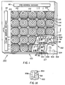
- a compact image capture and display device (digital camera) 200 are a photosensor array 100, a lenslet array 210, and a display 302.
- the lenslet array 210 is formed with achromatized refractive/diffractive lenslets 212 or refractive lenslets which are centered over photosensor sites (photosensors) 217 formed in the photosensor array 100.
- the lenslet array 210 replaces the typical single, long focal length multi-element lens that is spaced along one central axis in a camera. To be observed in Fig.
- each lenslet 212 is displaced relative to the fixed sensor-to-sensor distance as a function of its radial distance from the optical axis 213 of the central lenslet which is at the physical center of the array shown.
- the circular lines 215, appearing around the mechanical optical axis 214 of each lenslet 212, are topographical lines indicating equal changes in height of the lenslet's surface.
- An opaque mask 216 covers the areas between the lenslets 212 to prevent light from reaching the photosensor sites 217 other than by being focused by an associated lenslet.
- a typical implementation consists of 480 x 640 (or more) lenslets 212 with 3 photosensor sites 217 per lenslet, one for each of the primary colors, red, green, and blue.
- Other configurations of the lenslets may be used such as forming the outer periphery of each lenslet 212 as a square, hexagon, or circle, without detracting from the invention.
- the optical axis 214 of the lenslets 212 are located at a distance which becomes progressively larger than the center-to-center distance of the pixels generated by the photosensor array 100.
- a pixel is defined as the resultant image light focused by one lenslet 212 onto an associated one or group of photosensor sites 217.
- For a monochrome image only one photosensor is needed at one site.
- For a color image three photosensors are needed at three sites to generate the electrical signals for a pixel.
- the displacement of the lenslet's optical axis 214 increases radially from the center of the lenslet array.
- Decentering a lenslet tends to bend rays from off-axis field angles into the center of the lenslet's field of view.
- the optical axis of the lenslet By moving the optical axis of the lenslet further out radially with increasing distance from the center of the photosensor array 100, the angular location of an object at the center of the field of view for a given lenslet/photosensor pair originates from increasingly off-axis segments of the total field of view.
- the photosensor array 100 includes a silicon substrate for the photosensors and the interdispersed electronics: photosensor 20, multiplying current mirror 30, correlated double sampling circuit (CDS) 40, pixel display driver element 54, analog-to-digital converter 56, non-volatile memory 58, data bus 5O, and row and column address decoders 60 and 62, all to be described in more detail later.
- CDS correlated double sampling circuit
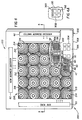
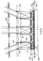
- the lenslet array 210 is located over the photosensor array 100 of photosensor sub arrays 222. Each photosensor sub arrays 222 is located at an associated photosensor site 217. Each group of photosensor sub arrays 222 is formed with red (R), green (G), and blue (B)sensors. The number of photosensor sites 217 corresponds in number to at least the number of lenslets 212 in the lenslet array 210. The lenslet array 210 is maintained a distance apart from the surfaces of the photosensors 222 by spacers 218 that serve the additional function of being light baffles.
- the opaque masks 216 on the lenslet array 210 combined with a field stop aperture plate 240 limit the field of view of any particular photosensor 222 so that it does not overlap the field of view of its neighbors by a large amount.
- the aperture plate 240 is positioned approximately O.5 mm to 2.0 mm from the surface of the lenslet array 210.
- the aperture plate 240 may be a layer of clear glass having a dyed photoresist mask pattern formed on one of it's surfaces.
- the center of the apertures in the aperture plate 240 are aligned to the center of the field of view of a corresponding lenslet.
- the spacing of the mechanical optical centers 214 increases as a function of each lenslet's position radially from the center of the array causing the aperture plate 240 to be slightly larger than the associated lenslet array 210.
- the combination of the opaque areas 216 with the aperture plate 240 and a given lenslet focal length determines the field of view for a photosensor site 217.
- the lenslet array 210 can be formed of etched quartz, or as an epoxy replica on a glass substrate or can be injection molded with plastic.
- the lenslets 212 combined with the appropriate field stop aperture plate 240, form images of a small segment of the field of view on each photosensor site 217.
- the lenslets 212 By forming the lenslets 212 with decentrations of the mechanical optical axis 214, which increase radially across the lenslet array, the angle which the axial ray incident on any particular lenslet makes with the surface normal to the plane of the lenslet array 210 will increase as a function of the particular lenslet's radial position on the array. Therefore, by appropriately forming the decenters of each lenslet each photosensor site 217 will view a different segment of a scene (image). Since each photosensor sub array 222 has its own lenslet there is no need to reinvert the image with a relay lens.
- Any camera system, incorporating the present invention, can be extremely compact and flat due to the integration of the above described circuitry which allows for the elimination of support circuit boards which in turn allows for a further decrease in the size of the camera.
- the camera can work in black and white or in color if three unit pixel subassemblies with color filters are formed at each photosensor site 217 to pass only assigned frequencies of incident radiation.
- through-holes 300 located adjacent to the photosensitive sub arrays 222 which through-holes 300 have been metalized to provide electrical contact to the emissive pixel 304.
- a transparent indium tin oxide layer 306 is the conductive layer that provides an electrical ground for all the emissive pixels 304.
- a glass layer 308 provides a transparent rigid support to the display.
- connections to the display are made by etching the through-holes 300 through the silicon substrate of the photosensor array 100 and plated through the holes using Deep Reactive Ion Etching technologies such as those implemented in the STS Systems Multiplex ICP High Density Plasma System or the Oxford Instruments Cryo-RIE unit. These new types of RIE etchers provide the ability to etch holes all the way through a silicon substrate to allow the formation of contacts through to the rear of the substrate.
- the conductive through contacts are formed by vapor depositing a metal, such as aluminum or gold, over the top and bottom of the entire silicon substrate. This is accomplished by vapor deposition, sputtering or electroplating the metal onto the silicon substrate.
- the top side of the metalization is then patterned using lithography to form traces 310A which lead from the pixel display driver element 54, on the top of the silicon substrate, to the plated through-holes 300. Since the metal has been deposited on the top and bottom of the silicon substrate, the through-holes 300 will be filled with a continuous piece of conductive metal which allows contact from the top traces 310A to the bottom metalization layer.
- traces 310B are formed from each plated through-hole 300 to a corresponding metal pad 312. Note: Fig. 1A is looking up from the bottom of the photosensor array 100.
- the bottom layer is lithographically patterned to form the metal pads 312 over the through-holes 300.
- the pads have the same (or smaller) area as the emissive pixel 304 on the display 302. In this way the metalization from an individual pixel driver circuit is connected to only one emissive pixel and is isolated from all other circuits and pixels.
- the pixel display driver 54 provides voltage signals proportional to the light emitted from the emissive pixels 304. In this fashion pixel display information can be viewed without the need to transmit data to an external display driver or external sensor clocking circuitry. Additionally only one power supply is needed to operate the CMOS based photosensor array and display as opposed to three used with standard CCD.
- the display 302 is comprised of a number of emissive pixels 304 capable of outputting either white, red, green, or blue light for presenting a Gray scale or color image of the photographic scene being captured or reviewed for capture. These emissive pixels 304 can be electroluminescent materials or organic light emitting diode materials such as those described in U.S.
- An indium tin oxide or other transparent conductor 306 is coated onto a glass substrate 308.
- the display 302 is operated by driving current through the emissive pixel 304 into the indium tin oxide 306 which is electrically grounded.
- the emissive pixels 304 are aligned to the metalized pads 312.
- a anisotropically conductive film 305 is sandwiched between the display 302 and the photosensor array 100 (as shown in Fig. 2 and Fig. 2A).
- the anisotropic conductive film 305 consists of conductive metal spheres 314 embedded in a polymeric binder. When the film 305 is subjected to pressure and an elevated temperature it will compress the metal spheres 314 into contact with each other in the area between the metalized pad 312 and the emissive pixel 304. The contacting metal spheres 314 will provide a conduction path between the pixel display driver element 54 and the emissive pixel 304. Note: in Fig. 2A the metal spheres 314 are not in contact with each other in the space between the back surface of 100 and the tin oxide layer 306.
- Suitable forms of making electrical connection between the metalized pads 312 and the emissive pixels 304 may be used, for example, in the embodiment of the invention shown in Figs. 4, 4A, and 5 low temperature eutectic bonding is used.
- Eutectic solder 307 is printed onto the metalized pads 312 and onto the back surface of the emissive pixels 304 using a silk-screening process. The electrical contact takes place when the two printed surfaces are pressed together with a uniform pressure per unit area at a slightly elevated temperature.
- an organic LED (type of display 302) can be formed on the back of the photosensor array 100 by using a lift off process (similar to the process described on pages 535-538 of Chapter 15 in "Silicon Processing for the VLSI Era” by Stanley Wolf, Ph.D and Richard N. Tauber, Ph.D., Lattice Press) to pattern the emissive pixels 304.
- the metalized and patterned photosensor array 100 is coated with photoresist on the rear surface and lithographically patterned to expose the metal pads 312 for the desired pixel.
- ITO coated cover glass is then contacted to the display using either a low temperature eutectic soldering process or an anisotropic conductive film process where temperature and pressure are applied to bond the emissive pixels 304 to the ITO coated glass.
- the pixel display driver 54 can be utilized to drive a reflective LCD type of display through the metalized through-holes 300 in the substrate.
- the resolution of the image which is displayed on the back of the camera is not necessarily the same as the resolution of the captured digital image. In some cases it is desirable to use a reduced number of pixels in the display section compared to the number of pixels in the captured image. This is due to the fact the number of pixels in the display unit (320 x 240 pixels) is relatively small compared to the number of pixels present in a high quality, high resolution digital image (640 x 480 or 1000 x 1500 pixels for example).
- the use of a reduced number of pixels in the display allows the use of a lower cost display and simplifies the data handling associated with displaying an image when the display is used as a viewfinder.
- Using a lower resolution display also allows for a more rapid update of the image on the display.
- a more rapid update eliminates the discontinuous or "jerky" display mode observed in currently produced digital cameras which utilize a display.
- the generation of the reduced size image is accomplished by binning the color pixel intensity values together and taking their mean in a smaller sub array of data used for the display. To accomplish this either the analog voltages or the digital intensity values from multiple adjacent photosensitive pixels are summed together and their mean is taken.
- the pixel display driver elements 54 which correspond in number to the number of emissive pixels then utilize the input presented from the smaller sub array of data to drive the display.
- the amplifiers and signal processing components of the compact image sensor are fabricated using CMOS type integrated circuit fabrication processes involving oxidation, diffusion, ion implantation, patterning with lithography and etching as described in Chapters 7-9, 12-13, and 15-16 of "Silicon Processing for the VLSI Era” by S. Wolf and R. Tauber.
- CMOS MOSFET used in forming amplifiers and logic circuits, and the structure of CCD and photodiode photosensors is described by Sze in Chapters 7, 8, and 13 of "Physics of Semiconductor Devices, Second Edition” (Bell Laboratories, Incorporated, Murray Hill, New Jersey, Wiley-Interscience publication).
- the circuit configurations for high sensitivity processing and data storage are described later in the specification.
- a unit pixel subassembly 10 forms part of the camera's photosensor array 100 (see array of Figs. 1 and 2).
- the unit pixel subassembly 10 is comprised of a photosensor 20, which may be, for example, a CCD device and/or a photodiode.
- the output 22 of the photosensor 20 is connected to a transfer gate 24, a reset gate 26, and a multiplying current mirror 30.
- the transfer gate 24 allows the charge, accumulated by the photosensor 20 during the exposure period, to be transferred to the multiplying current mirror 30 at the desired time.
- the reset gate 26 allows for the emptying of the photosensor's 20 accumulated charge from the previously completed exposure.
- the reset gate 26 is opened and closed when the camera's mechanical shutter is closed.
- the output 22 from the photosensor 20 is then integrated for a time equivalent to the previous exposure time so as to cancel dark current and noise. This cancellation occurs within a correlated double sampling circuit (CDS) 40.
- CDS correlated double sampling circuit
- the integrated signal from the CDS circuit 40 is digitized by an analog-to-digital converter 56 and the resulting digital value is stored in a non-volatile memory 58 which may be a SRAM memory.
- the digital value can be output to the main data bus 50 by accessing the unit pixel subassembly(s) through row and column address decoders, 60 and 62, respectively.
- the image data may be stored at site and/or downloaded after each capture.
- the photosensor array 100 is then ready for exposure to a new image.
- the output of the current mirror 30 can be a multiple of the current produced by the photosensor 20.
- the current multiplying effect is traditionally accomplished either by connecting the bases or gates of the transistors 32 1 through 32 n in parallel with each other or by making the emitter (or source) areas larger by an integral multiple of the emitter area of an input side transistor 34.
- Current mirrors of this type operate on the principle that the emitter base voltage (or the gate source voltage) for all the transistors on the output side of the current mirror are the same so that each of the collector (drain) currents is the same, and therefore the sum of the currents from the output side T o is an integral multiple of either the number of transistors in the output side or the ratio of the emitter areas.
- a transistor 36 can be added to the input side T i of the multiplying current mirror 30 to drive the bases (or gates) of the output side T o of the multiplying current mirror 30 and thereby reduce the effects of leakage current. This is known to reduce the non-ideality of the above equation to
- the output of the multiplying current mirror 30 is switched between two current amplifiers, amplifiers 42 and 44, with gains of +1 and - 1, respectively.
- amplifiers 42 and 44 When the photosensor 20 is receiving incident light its amplified current is switched through the +1 gain of amplifier 42 into an integrating amplifier 46 for a given amount of time and then after the shutter is closed the current is integrated through the -1 gain of amplifier 44 for an equal amount of time.
- This operation is known as dual slope, correlated double sampling, and it eliminates the effects of dark current and KTC noise. It differs from dual sample CDS in that the signal is switched through two different amplifiers depending on whether the signal represents the image data or the background data wherever dual time CDS uses the same amplification chain. It is another embodiment of the current invention to utilize dual sample CDS for noise reduction.
- Correlated double sampling reduces Johnson noise, flicker noise, and 1/f noise.
- a similar effect can be achieved by integrating the current from an opaquely masked photosensor through the - 1 gain of amplifier 44.
- Using an opaquely masked photosensor adjacent to the active photosensor 20 allows the correlated double sampling technique to be implemented in parallel and decreases readout time.
- the integration of the outputs of the current amplifiers 42 and 44 occurs simultaneously, thus eliminating the need to wait for two integration periods to have output data.
- small differences in dark current and noise can arise between them.
- multiplying current mirror in conjunction with the above memory and lenslet array allows for the decrease of the distance between the photosensor sites.
- larger distances between photosensor sites allows for the incorporation of more memory cells. Therefore there is a trade off between the multiplying factor associated with the multiplying current mirror and the number of images that can be stored in the compact imaging array. It is also an embodiment of the invention that the photogenerated charge of the photosensor can be stored after being multiplied by a multiplying current mirror.
- the integrated signal from the photosensors 20 is then digitized by an analog-to-digital converter (ADC) circuit 56.
- ADC analog-to-digital converter
- the output of the ADC is stored in the memory cell 58.
- there is only one memory cell at each unit pixel subassembly site it is also possible to locate multiple memory cells at each site which allows for the storage of multiple images on the photosensor array 100. This essentially allows the compact photosensor array to act as an optic array camera 200, complete with a lenslet array 210 and an emissive display 302 (see Fig. 5).
- the digital intensity data is accessed by strobing the memory cells 58 via row 60 and column 62 address decoders, in order to send data to the data bus 50.
- the incorporation of the row and column address decoder lines allows for addressing of subsections of the photosensitive array for more rapid image readout in a specific area of interest in the image.
- the pixel display driver 54 takes digital data from the non-volatile memory cell 58 and provides a voltage to an emissive pixel 304 that is proportional to the desired intensity in the captured scene.
- the emissive pixel 304 is part of a display formed as a matrix of emissive pixels 304. This configuration eliminates the need for clocking all of the digital image data out of the image capture sensor, providing it to a display driver circuit, and using row column addressing to generate the scene intensity at the emissive pixel, therefore, it is more compact and efficient.
- analog voltage generated at the correlated double sampling circuit 40 can be directly input to the pixel display driver 54 for fastest display or a simpler electronic configuration.
- Incorporating a display increases the utility of the digital camera by allowing the immediate review of images which have been captured in order to determine if the scene is to be kept or discarded. It also allows for the display of images captured earlier for viewing by others.
- the lenslet array 210 is formed with the array of achromatized refractive/diffractive lenslets 212 or refractive lenslets which are centered over photosensor sub arrays 222 formed into the photosensor array 100 (shown more clearly in Fig. 5).
- Fig. 4 To be observed in Fig. 4 is that the center of the mechanical optical axis 214 of each lenslet 212 is displaced relative to the fixed sensor-to-sensor distance as a function of its radial distance from the optical axis of the central lenslet.
- the circular lines 215 appearing around the mechanical optical axis 214 of each lenslet 212 are topographical lines indicating changes in height of the lenslet's surface.
- An opaque mask 216 fills the areas between the lenslets 212 to prevent light from reaching the photosensor array 100.
- the lenslet array 210 depicted in Fig. 4 represents only a small portion of an array that will be used in an actual camera. In an actual implementation approximately 150 X 100 lenslets are used to form the lenslet array 210.
- the photosensor sub array 222 is formed of an array of unit pixel subassemblies 10. Other configurations of the lenslets may be used such as forming the outer periphery of each lenslet as a square, hexagon, or circle, without detracting from the invention.
- Each photosensor sub array 222 has associated therewith a multiplying current mirror 30, a correlated double sampling circuit 40, an analog-to-digital converter 56, a sub array photosensor inverter 48, a non-volatile memory cell 58, and a pixel display driver 54.
- Each photosensor sub array 222 is ultimately attached to a data bus 50 which can output digital image data in response to signals from a row address decoder 60 and a column address decoder 62.
- an emissive pixel display 302 is connected to the compact digital camera as previously described.
- the lenslet array 210 is positioned over the photosensor array 100 and the photosensor sub array 222 that correspond in number to at least the number of lenslets used to form the lenslet array 210. In a three color environment up to one third of the sub array of photosensors 222 would be provided with a given color filter (red, green, or blue).
- the lenslet array 210 is maintained a distance apart from the surfaces of the photosensor sub array 222 by spacers 218 that may also serve the function of being baffles.
- the opaque masks 216 on the lenslet array 210 combined with a field stop aperture plate 240 limits the field of view of any particular photosensor sub array 222 so that it does not overlap the field of view of it neighbors by a large amount.
- the field stop aperture plate 240 is positioned approximately 0.5 mm to 3.0 mm from the surface of the lenslet array 210.
- the field stop aperture plate 240 may be a layer of clear glass having a photoresist mask pattern formed on one of it's surfaces.
- the center of the apertures in the aperture plate 240 are aligned to the center of the field of view of a corresponding lenslet.
- the spacing of the centers increases as a function of each lenslet's radial position radially from the center of the lenslet array causing the aperture plate to be slightly larger than the associated lens array.
- the combination of the opaque masks 216 with the aperture plate 240 and a given lenslet focal length determines the field of view for a photosensor sub array 222.
- the lenslet array 210 can be formed of etched quartz, injection molded plastic, or an epoxy replica on a glass substrate.
- the lenslets 212 combined with the appropriate field stop aperture plate 240, form images of a small segment of the field of view on each photosensor sub array 222.
- the lenslets 212 By forming the lenslets 212 with decentrations of the mechanical optical axis 214 which increase radially across the CCD array, the incident angle which the axial ray makes with the surface normal to the photosensor array will increase as a function of the radial position of the sub array with respect to the center of the photosensor array 100. Therefore, by appropriately adjusting the decenters of each lenslet, each photosensor sub array will view a different segment of the scene to be captured.
- the sub images from each photosensor sub array are digitally inverted and stitched with the other sub images to form a composite image. Therefore, the present inventive digital camera can be extremely compact and flat. This camera can work in black and white or in color if color filters are used on an appropriate number of photosensors in the photosensor sub array.
- the lenslet array can operate at low F/#'s (F/2.0) it is advantageous to minimize lenslet diameter (Increasing F/#) so as to minimize the space between lenslets and therefore the image sensor's overall dimensions. This may be accomplished if one incorporates circuitry to amplify the resulting signal from the photosensor.
- means for inverting the image at the sub array are incorporated in one embodiment. This means will consist of mapping the data from one photosensor to a memory location corresponding to a photosensor at a point which is a mirror image of the object reflected about the center of the sub array. It is also an embodiment of the invention to have the sub array images inverted by external circuitry or by means of digital image processing. By utilizing a multiplying current mirror to increase the photocurrent generated at each photosensor the lenslet diameter can be decreased.
- a multiplexing and clocking circuit 80 samples, in turn, the output from each pixel subassembly 10 in an associated photosensor sub array 222, and passes the output 22 to multiplying current mirror 30.
- the photosensor current from the multiplying current mirror 30 is integrated by the CDS circuit 40 and then digitized by the analog-to-digital converter 56.
- the sub array photosensor inverter 48 takes data from a given photosensor and maps it to a memory location where an equivalent inverted photosensor would lie. This allows the resulting sub images from each sub array of photosensors to be stitched together to form a larger composite image.
- the invention utilizes digital image capture and processing to eliminate the need for an additional array of relay lenslets to invert the sub images formed by each objective lenslet 212. It also eliminates the need for a third array of field lenses which may be utilized to maintain illumination uniformity across the lenslet's field of view.
- the output of the analog-to-digital converter 56 is stored in the memory cells 58 after inversion by the sub array photosensor Inverter 48. It is also possible to assign a group of memory cells to each photosensor sub array 222. This would allow the compact photosensor array 210 to act as a digital camera.
- the digital intensity data is accessed by strobing the memory cells 58 via row and column address decoder lines 60 and 62, respectively, in order to send data to the data bus 50.
- the incorporation of the row and column address decoder allows for the addressing of subsections of the photosensor array 100 for more rapid image readout in a specific area of interest in the image
- Display data from the non-volatile memory 58 is used to generate a voltage which is driven through the metalization in the through-holes 300 to the emissive pixels 304 to form an image of the data stored in memory on the display 302.
- the display 302 is comprised of a series of emissive pixels 304 coated onto a layer of electrically grounded indium tin oxide 306 on a glass substrate 308.
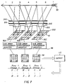
- an object 90 (arrow) is imaged onto photosensor sub arrays 222.
- Each lenslet 212 views a different segment of the field of view.
- the segment 1-3 of the arrow forms an inverted image 92A that impinges on its respective photosensor sub array 222.
- the segment 3-5 of the arrow 90 forms an inverted image 92B that impinges on its respective photosensor sub array 222.
- the segment 5-7 forming the inverted image 92C. Noted in the drawing is that the images 92A through 92C do not form, from left to right, a continuous image of the arrow 90.
- point 1 is adjacent point 5 and that point 3 is adjacent point 7 at the surfaces of the photosensor sub array 222. That is, if the sub-images of the arrow 90 were simply stitched together, the overall mosaic (composite) image would be scrambled and unusable.
- each photosensor sub array 222 To arrange the pixel image data in proper order the charges from the matrix of photosensors 20 In each photosensor sub array 222 are first clocked out and multiplexed through their respective current multiplying circuit, correlated double sampling circuitry, and digitised by the ADC.
- the digital data from a pixel, representing an image, in each photosensor sub array 222 is positionally inverted with respect to the center of each photosensor sub array 222. Therefore, a sub array photosensor inverter 48 is needed to take the pixel data from a pixel located at point A and to store it in a memory cell 58 which is inverted with respect to the central pixel of the photosensor sub array.
- pixel A would be stored in the memory 58 at a location corresponding to D.
- the overall mosaic composite image is then built up for use by an output device 110 which is for this instance the emissive display 302.
- a computer and/or a digital printer may also be used to form the output image.
- overall image pixel data is generated from the photosensor sub array by digitally stitching the sub-images back together to form a composite image. This is accomplished by taking the row data from each sub array in turn and adding it to the row data for the next sub array until the end of the array is reached. Then the address for the next column of row data, at the farthest point on the array, is used to start building the next row of image data by adding the row data from the next sub array until the end of the line of sub arrays is reached, at which point the address pointer moves to the beginning of the next column. In some embodiments it may be useful to have some image overlap from one sub array to the next. This would require the address decoding technique to be able to determine which location in a sub array row is to be used as the first pixel from that row.
Abstract
Description
n = number of transistors on the output side "To" of the current mirror, or
β = transistor current gain (typically between 50 and 200 for bipolar transistors).

- 10
- unit pixel subassembly
- 20
- photosensor
- 22
- output
- 24
- transfer gate
- 26
- reset gate
- 30
- multiplying current mirror
- 321 -32n
- transistors
- 34
- input side transistor
- 36
- transistor
- 40
- correlated double sampling circuit (CDS)
- 42
- current amplifiers
- 44
- current amplifiers
- 46
- integrating amplifier
- 48
- sub array photosensor inverter
- 50
- data bus
- 54
- pixel display driver element
- 56
- analog-to-digital converter
- 58
- memory
- 60
- row address decoder line
- 62
- column address decoder line
- 80
- multiplexing and clocking circuit
- 90
- object (arrow)
- 100
- photosensor array
- 200
- compact image capture and display device (digital camera)
- 210
- lenslet array
- 212
- lenslets
- 213
- optical axis
- 214
- mechanical optical axis
- 215
- circular lines
- 216
- opaque mask
- 217
- photosensor sites
- 218
- spacers
- 222
- photosensor sub array
- 300
- through-holes
- 302
- display
- 304
- emissive pixel
- 305
- anisotropically conductive film
- 306
- transparent indium tin oxide layer
- 307
- eutectic solder
- 308
- glass layer
- 310A
- traces
- 310B
- traces
- 312
- metal pad
- 314
- conductive metal spheres
Claims (10)
- A compact image capture and display device, comprising:an array of spaced apart radiation sensors for providing output signals that are a function of the amount of incident radiation from an image onto each radiation sensor;array electronics dispersed in the spaces between the spaced apart radiation sensors for receiving and processing the provided output signals to facilitate image capture;a lens array positioned so as to focus the radiation of an image to be captured onto said radiation sensors; anda display connected in close proximity to said array electronics to receive the processed output signals from said array electronics and to display the image captured by said radiation sensors.
- The compact image capture and display device according to Claim 1 and further comprising:a planar support member having said array of radiation sensors formed on one surface and said display formed on an opposite surface and having connections passing through said planar support member to connect said display to said array electronics.
- The compact image capture and display device according to Claim 2 wherein said support member is a semiconductor material having said array of radiation sensors formed integrally therein.
- The compact image capture and display device according to Claim 1 wherein said display is an array of LEDs.
- The compact image capture and display device according to Claim 1 wherein said display is an array of organic LEDs.
- An image capture and display device comprising:an array of spaced apart groups of radiation sensors for providing output signals that are a function of the color of incident radiation from an image onto each radiation sensor;array electronics dispersed in the spaces between the spaced apart groups of radiation sensors for receiving and processing the provided output signals;a lens array positioned so as to focus the wavelengths of radiation from an image to be captured onto associated radiation sensors in each of the groups of said radiation sensors such that each radiation sensor in a group provides an output signal that is stored as a function of its colors; anda display means for receiving the processed output signals from said array electronics and for visually displaying the images captured onto the radiation sensors.
- The image capture and display device according to Claim 6 and further comprising:a planar support member having said array of radiation sensors formed on one surface and said display formed on an opposite surface and having connections passing through said planar support member to connect said display to said array electronics.
- The image capture and display device according to Claim 7 wherein said support member is a semiconductor material having said array of radiation sensors formed integrally therein.
- A compact image capture and display device, comprising:a photosensor array of current generating photosensors each in combination with an associated multiplying current mirror located adjacent thereto and comprised of one input transistor and at least two output transistors where the generated photocurrent from each photosensor is multiplied by an integer equal to the number of output transistors in the associated multiplying current mirror with the output of the current mirror being forwarded to a digitizing and memory means located adjacent to an associated current mirror for storage, a display connected to display the digitized output of the current mirrors.
- A compact digital camera, comprising:a lenslet array comprised of a plurality of lenslets, each lenslet having a decentration corresponding to its radial position in the lenslet array so that the axial ray of each lenslet views a different segment of a total field of view;a color photosensor array comprised of a plurality of sub arrays of photosensors wherein each sub array of photosensors is comprised of sets of Red, Green, and Blue color sensitive photosensors, each sub array of photosensors being positioned along the axial ray of a respective lenslet;a field limiting baffle comprised of at least one aperture plate where the center of the apertures are positioned to lie along the axial ray of a respective lenslet; anda color display for displaying the colors sensed said color photosensor array.
Applications Claiming Priority (2)
| Application Number | Priority Date | Filing Date | Title |
|---|---|---|---|
| US88244697A | 1997-06-25 | 1997-06-25 | |
| US882446 | 1997-06-25 |
Publications (2)
| Publication Number | Publication Date |
|---|---|
| EP0893915A2 true EP0893915A2 (en) | 1999-01-27 |
| EP0893915A3 EP0893915A3 (en) | 2000-01-05 |
Family
ID=25380590
Family Applications (1)
| Application Number | Title | Priority Date | Filing Date |
|---|---|---|---|
| EP98201979A Withdrawn EP0893915A3 (en) | 1997-06-25 | 1998-06-12 | Compact image sensor with display integrally attached |
Country Status (2)
| Country | Link |
|---|---|
| EP (1) | EP0893915A3 (en) |
| JP (1) | JPH11127390A (en) |
Cited By (19)
| Publication number | Priority date | Publication date | Assignee | Title |
|---|---|---|---|---|
| EP1206126A2 (en) * | 2000-10-13 | 2002-05-15 | Canon Kabushiki Kaisha | Image pickup apparatus |
| EP1215729A2 (en) * | 2000-12-18 | 2002-06-19 | Canon Kabushiki Kaisha | Image pickup apparatus |
| EP1377039A2 (en) * | 2002-06-24 | 2004-01-02 | Canon Kabushiki Kaisha | Compound eye image pickup apparatus and electronic apparatus equipped therewith |
| GB2409944A (en) * | 2004-01-09 | 2005-07-13 | Agilent Technologies Inc | Photo-array layout for monitoring image statistics |
| US6975355B1 (en) | 2000-02-22 | 2005-12-13 | Pixim, Inc. | Multiple sampling via a time-indexed method to achieve wide dynamic ranges |
| WO2006131889A2 (en) * | 2005-06-10 | 2006-12-14 | Universita' Degli Studi Di Pavia | Image-taking optimisation device, method and optical component therefor |
| WO2007005688A1 (en) * | 2005-06-30 | 2007-01-11 | Agc Flat Glass North America, Inc. | Monolithic image perception device and method |
| WO2010078563A1 (en) * | 2009-01-05 | 2010-07-08 | Applied Quantum Technologies, Inc. | Multiscale optical system using a lens array |
| EP2561547A1 (en) * | 2010-04-20 | 2013-02-27 | Bae Systems Australia Limited | Directed infra-red countermeasure system |
| US8478081B2 (en) | 2005-06-30 | 2013-07-02 | Agc Flat Glass North America, Inc. | Monolithic image perception device and method |
| US8629930B2 (en) | 2009-10-14 | 2014-01-14 | Fraunhofer-Gesellschaft Zur Foerderung Der Angewandten Forschung E.V. | Device, image processing device and method for optical imaging |
| US8830377B2 (en) | 2010-01-04 | 2014-09-09 | Duke University | Monocentric lens-based multi-scale optical systems and methods of use |
| US9395617B2 (en) | 2009-01-05 | 2016-07-19 | Applied Quantum Technologies, Inc. | Panoramic multi-scale imager and method therefor |
| US9432591B2 (en) | 2009-01-05 | 2016-08-30 | Duke University | Multiscale optical system having dynamic camera settings |
| US9494771B2 (en) | 2009-01-05 | 2016-11-15 | Duke University | Quasi-monocentric-lens-based multi-scale optical system |
| US9635253B2 (en) | 2009-01-05 | 2017-04-25 | Duke University | Multiscale telescopic imaging system |
| US10725280B2 (en) | 2009-01-05 | 2020-07-28 | Duke University | Multiscale telescopic imaging system |
| CN114323310A (en) * | 2021-12-28 | 2022-04-12 | 中国科学院光电技术研究所 | High-resolution Hartmann wavefront sensor |
| US11630339B2 (en) | 2019-01-16 | 2023-04-18 | Sony Semiconductor Solutions Corporation | Display element and projection type display apparatus |
Families Citing this family (3)
| Publication number | Priority date | Publication date | Assignee | Title |
|---|---|---|---|---|
| US7511749B2 (en) * | 2003-12-18 | 2009-03-31 | Aptina Imaging Corporation | Color image sensor having imaging element array forming images on respective regions of sensor elements |
| JP2007304324A (en) * | 2006-05-11 | 2007-11-22 | Konica Minolta Holdings Inc | Display panel |
| JP5463718B2 (en) * | 2009-04-16 | 2014-04-09 | ソニー株式会社 | Imaging device |
Citations (6)
| Publication number | Priority date | Publication date | Assignee | Title |
|---|---|---|---|---|
| US5340978A (en) * | 1992-09-30 | 1994-08-23 | Lsi Logic Corporation | Image-sensing display panels with LCD display panel and photosensitive element array |
| US5461425A (en) * | 1994-02-15 | 1995-10-24 | Stanford University | CMOS image sensor with pixel level A/D conversion |
| US5471515A (en) * | 1994-01-28 | 1995-11-28 | California Institute Of Technology | Active pixel sensor with intra-pixel charge transfer |
| US5610390A (en) * | 1994-10-03 | 1997-03-11 | Fuji Photo Optical Co., Ltd. | Solid-state image pickup device having microlenses each with displaced optical axis |
| EP0833502A2 (en) * | 1996-09-26 | 1998-04-01 | Eastman Kodak Company | Compact image capture device with local image storage |
| EP0840502A2 (en) * | 1996-11-04 | 1998-05-06 | Eastman Kodak Company | Compact digital camera with segmented fields of view |
-
1998
- 1998-06-12 EP EP98201979A patent/EP0893915A3/en not_active Withdrawn
- 1998-06-24 JP JP10176889A patent/JPH11127390A/en active Pending
Patent Citations (6)
| Publication number | Priority date | Publication date | Assignee | Title |
|---|---|---|---|---|
| US5340978A (en) * | 1992-09-30 | 1994-08-23 | Lsi Logic Corporation | Image-sensing display panels with LCD display panel and photosensitive element array |
| US5471515A (en) * | 1994-01-28 | 1995-11-28 | California Institute Of Technology | Active pixel sensor with intra-pixel charge transfer |
| US5461425A (en) * | 1994-02-15 | 1995-10-24 | Stanford University | CMOS image sensor with pixel level A/D conversion |
| US5610390A (en) * | 1994-10-03 | 1997-03-11 | Fuji Photo Optical Co., Ltd. | Solid-state image pickup device having microlenses each with displaced optical axis |
| EP0833502A2 (en) * | 1996-09-26 | 1998-04-01 | Eastman Kodak Company | Compact image capture device with local image storage |
| EP0840502A2 (en) * | 1996-11-04 | 1998-05-06 | Eastman Kodak Company | Compact digital camera with segmented fields of view |
Cited By (40)
| Publication number | Priority date | Publication date | Assignee | Title |
|---|---|---|---|---|
| US6975355B1 (en) | 2000-02-22 | 2005-12-13 | Pixim, Inc. | Multiple sampling via a time-indexed method to achieve wide dynamic ranges |
| US7639297B2 (en) | 2000-10-13 | 2009-12-29 | Canon Kabushiki Kaisha | Image pickup apparatus |
| EP1206126A3 (en) * | 2000-10-13 | 2004-07-14 | Canon Kabushiki Kaisha | Image pickup apparatus |
| EP1206126A2 (en) * | 2000-10-13 | 2002-05-15 | Canon Kabushiki Kaisha | Image pickup apparatus |
| US6952228B2 (en) | 2000-10-13 | 2005-10-04 | Canon Kabushiki Kaisha | Image pickup apparatus |
| EP1215729A2 (en) * | 2000-12-18 | 2002-06-19 | Canon Kabushiki Kaisha | Image pickup apparatus |
| EP1215729A3 (en) * | 2000-12-18 | 2004-01-14 | Canon Kabushiki Kaisha | Image pickup apparatus |
| EP1377039A2 (en) * | 2002-06-24 | 2004-01-02 | Canon Kabushiki Kaisha | Compound eye image pickup apparatus and electronic apparatus equipped therewith |
| EP1377039A3 (en) * | 2002-06-24 | 2005-09-21 | Canon Kabushiki Kaisha | Compound eye image pickup apparatus and electronic apparatus equipped therewith |
| GB2409944A (en) * | 2004-01-09 | 2005-07-13 | Agilent Technologies Inc | Photo-array layout for monitoring image statistics |
| GB2409944B (en) * | 2004-01-09 | 2009-02-18 | Agilent Technologies Inc | Photo-array layout for monitoring image statistics |
| WO2006131889A3 (en) * | 2005-06-10 | 2007-04-12 | Univ Pavia | Image-taking optimisation device, method and optical component therefor |
| WO2006131889A2 (en) * | 2005-06-10 | 2006-12-14 | Universita' Degli Studi Di Pavia | Image-taking optimisation device, method and optical component therefor |
| WO2007005688A1 (en) * | 2005-06-30 | 2007-01-11 | Agc Flat Glass North America, Inc. | Monolithic image perception device and method |
| JP2009524120A (en) * | 2005-06-30 | 2009-06-25 | エージーシー フラット グラス ノース アメリカ,インコーポレイテッド | Integrated image recognition apparatus and method |
| US8478081B2 (en) | 2005-06-30 | 2013-07-02 | Agc Flat Glass North America, Inc. | Monolithic image perception device and method |
| US7796841B2 (en) | 2005-06-30 | 2010-09-14 | Agc Flat Glass North America, Inc. | Monolithic image perception device and method |
| RU2444059C2 (en) * | 2005-06-30 | 2012-02-27 | Эй-Джи-Си Флэт Гласс Норт Америкэ, Инк. | Integrated device and method of reading images |
| US9092689B2 (en) | 2005-06-30 | 2015-07-28 | Agc Flat Glass North America, Inc. | Monolithic image perception device and method |
| CN101253515B (en) * | 2005-06-30 | 2012-09-26 | 北美Agc平板玻璃公司 | Monolithic image perception device and method |
| US9432591B2 (en) | 2009-01-05 | 2016-08-30 | Duke University | Multiscale optical system having dynamic camera settings |
| US9635253B2 (en) | 2009-01-05 | 2017-04-25 | Duke University | Multiscale telescopic imaging system |
| US10725280B2 (en) | 2009-01-05 | 2020-07-28 | Duke University | Multiscale telescopic imaging system |
| EP3264756A1 (en) * | 2009-01-05 | 2018-01-03 | Applied Quantum Technologies, Inc. | Multiscale optical system |
| US9762813B2 (en) | 2009-01-05 | 2017-09-12 | Duke University | Monocentric lens-based multi-scale optical systems and methods of use |
| US9494771B2 (en) | 2009-01-05 | 2016-11-15 | Duke University | Quasi-monocentric-lens-based multi-scale optical system |
| WO2010078563A1 (en) * | 2009-01-05 | 2010-07-08 | Applied Quantum Technologies, Inc. | Multiscale optical system using a lens array |
| US8259212B2 (en) | 2009-01-05 | 2012-09-04 | Applied Quantum Technologies, Inc. | Multiscale optical system |
| US9256056B2 (en) | 2009-01-05 | 2016-02-09 | Duke University | Monocentric lens-based multi-scale optical systems and methods of use |
| US9395617B2 (en) | 2009-01-05 | 2016-07-19 | Applied Quantum Technologies, Inc. | Panoramic multi-scale imager and method therefor |
| US8629930B2 (en) | 2009-10-14 | 2014-01-14 | Fraunhofer-Gesellschaft Zur Foerderung Der Angewandten Forschung E.V. | Device, image processing device and method for optical imaging |
| US8830377B2 (en) | 2010-01-04 | 2014-09-09 | Duke University | Monocentric lens-based multi-scale optical systems and methods of use |
| EP2561547A1 (en) * | 2010-04-20 | 2013-02-27 | Bae Systems Australia Limited | Directed infra-red countermeasure system |
| EP2561547A4 (en) * | 2010-04-20 | 2013-12-04 | Bae Systems Australia Ltd | Directed infra-red countermeasure system |
| CN103221966B (en) * | 2010-09-13 | 2016-08-31 | 北美Agc平板玻璃公司 | Monolithic image perception apparatus and method |
| CN103221966A (en) * | 2010-09-13 | 2013-07-24 | 北美Agc平板玻璃公司 | Monolithic image perception device and method |
| EP2616994A1 (en) * | 2010-09-13 | 2013-07-24 | AGC Flat Glass North America, Inc. | Monolithic image perception device and method |
| US11630339B2 (en) | 2019-01-16 | 2023-04-18 | Sony Semiconductor Solutions Corporation | Display element and projection type display apparatus |
| CN114323310A (en) * | 2021-12-28 | 2022-04-12 | 中国科学院光电技术研究所 | High-resolution Hartmann wavefront sensor |
| CN114323310B (en) * | 2021-12-28 | 2023-05-26 | 中国科学院光电技术研究所 | High-resolution Hartmann wavefront sensor |
Also Published As
| Publication number | Publication date |
|---|---|
| EP0893915A3 (en) | 2000-01-05 |
| JPH11127390A (en) | 1999-05-11 |
Similar Documents
| Publication | Publication Date | Title |
|---|---|---|
| EP0893915A2 (en) | Compact image sensor with display integrally attached | |
| US6141048A (en) | Compact image capture device | |
| US6137535A (en) | Compact digital camera with segmented fields of view | |
| US11720059B2 (en) | Method, apparatus and system providing holographic layer as micro-lens and color filter array in an imager | |
| EP1031239B1 (en) | Optoelectronic camera and method for image formatting in the same | |
| US6124974A (en) | Lenslet array systems and methods | |
| KR100263579B1 (en) | Solid state image pick-up device equipped with charge coupled device having incident surface alignable with focal plane | |
| US5973844A (en) | Lenslet array systems and methods | |
| JP3028185U (en) | X-ray diagnostic device | |
| JP2003318381A (en) | Solid-state imaging device and camera | |
| US9661241B2 (en) | Solid-state imaging device and electronic apparatus | |
| JP3478796B2 (en) | Solid-state imaging device | |
| US6753915B1 (en) | Photoelectric Conversion Apparatus and Image Pickup Apparatus having an Optimally Positioned Driving Wire | |
| JPH0730089A (en) | Image sensor | |
| EP0833502A2 (en) | Compact image capture device with local image storage | |
| Graeve et al. | Amorphous silicon image sensor for x-ray applications | |
| US6545711B1 (en) | Photo diode pixel sensor array having a guard ring | |
| US5864132A (en) | Full image optical detector with spaced detector pixels | |
| CN1448696A (en) | Photometry/ranging solid state image pick-up device and image pick-up apparatus using such device | |
| Duparré et al. | Latest developments in micro-optical artificial compound eyes: a promising approach for next generation ultracompact machine vision | |
| KR100355992B1 (en) | A digital radiation image processing system | |
| Gilmore et al. | The LSST camera system overview | |
| US6281486B1 (en) | Off-axis image correction with spaced photodetectors | |
| TW432872B (en) | Imaging circuit and method of spatial compensation | |
| JPH06339084A (en) | Solid-state image pickup element |
Legal Events
| Date | Code | Title | Description |
|---|---|---|---|
| PUAI | Public reference made under article 153(3) epc to a published international application that has entered the european phase |
Free format text: ORIGINAL CODE: 0009012 |
|
| AK | Designated contracting states |
Kind code of ref document: A2 Designated state(s): AT BE CH CY DE DK ES FI FR GB GR IE IT LI LU MC NL PT SE |
|
| AX | Request for extension of the european patent |
Free format text: AL;LT;LV;MK;RO;SI |
|
| PUAL | Search report despatched |
Free format text: ORIGINAL CODE: 0009013 |
|
| AK | Designated contracting states |
Kind code of ref document: A3 Designated state(s): AT BE CH CY DE DK ES FI FR GB GR IE IT LI LU MC NL PT SE |
|
| AX | Request for extension of the european patent |
Free format text: AL;LT;LV;MK;RO;SI |
|
| AKX | Designation fees paid | ||
| REG | Reference to a national code |
Ref country code: DE Ref legal event code: 8566 |
|
| STAA | Information on the status of an ep patent application or granted ep patent |
Free format text: STATUS: THE APPLICATION IS DEEMED TO BE WITHDRAWN |
|
| 18D | Application deemed to be withdrawn |
Effective date: 20000706 |