EP0897616B1 - Frequency synthesizer with temperature compensation and frequency multiplication and method of providing the same - Google Patents
Frequency synthesizer with temperature compensation and frequency multiplication and method of providing the same Download PDFInfo
- Publication number
- EP0897616B1 EP0897616B1 EP97904231.4A EP97904231A EP0897616B1 EP 0897616 B1 EP0897616 B1 EP 0897616B1 EP 97904231 A EP97904231 A EP 97904231A EP 0897616 B1 EP0897616 B1 EP 0897616B1
- Authority
- EP
- European Patent Office
- Prior art keywords
- frequency
- temperature
- oscillator
- modulus
- coupled
- Prior art date
- Legal status (The legal status is an assumption and is not a legal conclusion. Google has not performed a legal analysis and makes no representation as to the accuracy of the status listed.)
- Expired - Lifetime
Links
Images


Classifications
-
- H—ELECTRICITY
- H03—ELECTRONIC CIRCUITRY
- H03L—AUTOMATIC CONTROL, STARTING, SYNCHRONISATION, OR STABILISATION OF GENERATORS OF ELECTRONIC OSCILLATIONS OR PULSES
- H03L7/00—Automatic control of frequency or phase; Synchronisation
- H03L7/06—Automatic control of frequency or phase; Synchronisation using a reference signal applied to a frequency- or phase-locked loop
- H03L7/16—Indirect frequency synthesis, i.e. generating a desired one of a number of predetermined frequencies using a frequency- or phase-locked loop
- H03L7/18—Indirect frequency synthesis, i.e. generating a desired one of a number of predetermined frequencies using a frequency- or phase-locked loop using a frequency divider or counter in the loop
- H03L7/197—Indirect frequency synthesis, i.e. generating a desired one of a number of predetermined frequencies using a frequency- or phase-locked loop using a frequency divider or counter in the loop a time difference being used for locking the loop, the counter counting between numbers which are variable in time or the frequency divider dividing by a factor variable in time, e.g. for obtaining fractional frequency division
-
- H—ELECTRICITY
- H03—ELECTRONIC CIRCUITRY
- H03L—AUTOMATIC CONTROL, STARTING, SYNCHRONISATION, OR STABILISATION OF GENERATORS OF ELECTRONIC OSCILLATIONS OR PULSES
- H03L1/00—Stabilisation of generator output against variations of physical values, e.g. power supply
- H03L1/02—Stabilisation of generator output against variations of physical values, e.g. power supply against variations of temperature only
- H03L1/022—Stabilisation of generator output against variations of physical values, e.g. power supply against variations of temperature only by indirect stabilisation, i.e. by generating an electrical correction signal which is a function of the temperature
- H03L1/026—Stabilisation of generator output against variations of physical values, e.g. power supply against variations of temperature only by indirect stabilisation, i.e. by generating an electrical correction signal which is a function of the temperature by using a memory for digitally storing correction values
-
- H—ELECTRICITY
- H03—ELECTRONIC CIRCUITRY
- H03L—AUTOMATIC CONTROL, STARTING, SYNCHRONISATION, OR STABILISATION OF GENERATORS OF ELECTRONIC OSCILLATIONS OR PULSES
- H03L7/00—Automatic control of frequency or phase; Synchronisation
- H03L7/06—Automatic control of frequency or phase; Synchronisation using a reference signal applied to a frequency- or phase-locked loop
- H03L7/16—Indirect frequency synthesis, i.e. generating a desired one of a number of predetermined frequencies using a frequency- or phase-locked loop
- H03L7/18—Indirect frequency synthesis, i.e. generating a desired one of a number of predetermined frequencies using a frequency- or phase-locked loop using a frequency divider or counter in the loop
- H03L7/183—Indirect frequency synthesis, i.e. generating a desired one of a number of predetermined frequencies using a frequency- or phase-locked loop using a frequency divider or counter in the loop a time difference being used for locking the loop, the counter counting between fixed numbers or the frequency divider dividing by a fixed number
- H03L7/185—Indirect frequency synthesis, i.e. generating a desired one of a number of predetermined frequencies using a frequency- or phase-locked loop using a frequency divider or counter in the loop a time difference being used for locking the loop, the counter counting between fixed numbers or the frequency divider dividing by a fixed number using a mixer in the loop
-
- H—ELECTRICITY
- H03—ELECTRONIC CIRCUITRY
- H03L—AUTOMATIC CONTROL, STARTING, SYNCHRONISATION, OR STABILISATION OF GENERATORS OF ELECTRONIC OSCILLATIONS OR PULSES
- H03L7/00—Automatic control of frequency or phase; Synchronisation
- H03L7/06—Automatic control of frequency or phase; Synchronisation using a reference signal applied to a frequency- or phase-locked loop
- H03L7/16—Indirect frequency synthesis, i.e. generating a desired one of a number of predetermined frequencies using a frequency- or phase-locked loop
- H03L7/18—Indirect frequency synthesis, i.e. generating a desired one of a number of predetermined frequencies using a frequency- or phase-locked loop using a frequency divider or counter in the loop
- H03L7/197—Indirect frequency synthesis, i.e. generating a desired one of a number of predetermined frequencies using a frequency- or phase-locked loop using a frequency divider or counter in the loop a time difference being used for locking the loop, the counter counting between numbers which are variable in time or the frequency divider dividing by a factor variable in time, e.g. for obtaining fractional frequency division
- H03L7/1974—Indirect frequency synthesis, i.e. generating a desired one of a number of predetermined frequencies using a frequency- or phase-locked loop using a frequency divider or counter in the loop a time difference being used for locking the loop, the counter counting between numbers which are variable in time or the frequency divider dividing by a factor variable in time, e.g. for obtaining fractional frequency division for fractional frequency division
- H03L7/1976—Indirect frequency synthesis, i.e. generating a desired one of a number of predetermined frequencies using a frequency- or phase-locked loop using a frequency divider or counter in the loop a time difference being used for locking the loop, the counter counting between numbers which are variable in time or the frequency divider dividing by a factor variable in time, e.g. for obtaining fractional frequency division for fractional frequency division using a phase accumulator for controlling the counter or frequency divider
-
- H—ELECTRICITY
- H03—ELECTRONIC CIRCUITRY
- H03L—AUTOMATIC CONTROL, STARTING, SYNCHRONISATION, OR STABILISATION OF GENERATORS OF ELECTRONIC OSCILLATIONS OR PULSES
- H03L1/00—Stabilisation of generator output against variations of physical values, e.g. power supply
- H03L1/02—Stabilisation of generator output against variations of physical values, e.g. power supply against variations of temperature only
- H03L1/022—Stabilisation of generator output against variations of physical values, e.g. power supply against variations of temperature only by indirect stabilisation, i.e. by generating an electrical correction signal which is a function of the temperature
- H03L1/027—Stabilisation of generator output against variations of physical values, e.g. power supply against variations of temperature only by indirect stabilisation, i.e. by generating an electrical correction signal which is a function of the temperature by using frequency conversion means which is variable with temperature, e.g. mixer, frequency divider, pulse add/substract logic circuit
Definitions
- the present invention relates generally to frequency synthesizers used in conjunction with piezoelectric frequency oscillators in a multi-channel radio and, in particular, to a frequency synthesizer with temperature compensation and frequency multiplication and method of providing the same.
- Frequency synthesizers have typically been provided with reference frequency signals from crystal controlled frequency oscillators having temperature compensation circuits for use in frequency stabilized radio communications. These compensation circuits may be composed of analog or digital devices and are used to provide a relatively flat frequency output over temperature.
- a capacitive element is provided to allow absolute adjustment of the final frequency of the oscillator. This capacitive element is generally either in the form of a trim capacitor or an analog varactor controlled by an applied DC voltage. By adjusting this capacitance, the user is able to adjust (warp) the oscillator onto a desired final frequency.
- the frequency adjustment range (warpability) of a crystal controlled frequency oscillator is limited by the physical size of the crystal and its electrodes.
- An increase in warpability necessitates the use of a crystal with an increased width-to-thickness ratio.
- an increase of width-to-thickness ratio causes a crystal to be more fragile and more costly than a crystal without a higher warpability requirement.
- the long term stability of a highly warpable crystal is compromised due to its more sensitive nature.
- Warpability may also be increased by the use of a capacitive element having a larger tuning range.
- this typically requires that the element be of a physically larger size.
- the size of the element may bring other problems.
- analog varactors are necessarily large and do not scale as well with integrated circuit process shrinks as do digital circuits.
- these reactive elements have their own variation with temperature, outside of the crystal temperature variation, which must be controlled by an applied voltage, as well as being compensated along with the crystal temperature variation.
- a high supply voltage is needed for bias.
- this restricts the use of a lower voltage, single-supply operated frequency oscillator.
- the oscillator AC voltage output swing must also be controlled to prevent the varactor from conducting.
- the frequency is manipulated three or more times.
- a crystal controlled frequency oscillator has temperature compensation circuitry applied to provide a relatively flat frequency output over temperature.
- the oscillator is warped onto a desired frequency.
- this corrected oscillator frequency is multiplied in a phase locked loop (PLL) to produce the higher frequencies required in local oscillators in radio communications equipment. It would be advantageous to temperature compensate a synthesizer output frequency with a single element without incorporating additional synthesizer elements.
- PLL phase locked loop
- a temperature compensated frequency oscillator using a PLL frequency synthesizer which: achieves more accurate, linear and repeatable temperature compensation with more simplified circuitry; does not need tunable reactive elements to warp the oscillator onto the desired frequency thereby allowing smaller, less expensive elements to be used; provides a temperature-dependent frequency multiplying element whereby temperature compensation of the crystal oscillator and other circuit elements in the frequency synthesizer is achieved,
- the present invention provides a frequency synthesizer with temperature compensation and frequency multiplication, as claimed in claim 1.
- the present invention provides a method of temperature compensating and multiplying a frequency output in a frequency synthesizer, as claimed in claim 8.
- FIG. 1 shows a prior art frequency source 10 providing a multiplied and temperature compensated frequency output 12.
- a temperature compensated frequency oscillator 14 is coupled to a temperature-independent frequency multiplier 16 which provides the desired frequency output 12.
- the frequency oscillator 14 includes a crystal oscillator 18, at least one frequency warp element 20 which is typically a varactor, a temperature compensation controller 22, a temperature sensor 24, and a memory 26.
- the memory 26 contains a preprogrammed lookup table of temperature compensating data for the crystal that correspond to predetermined temperature varying voltage signals provided by the temperature sensor 24.
- the sensor 24 is located in proximity to the crystal to reduce errors which may arise due to temperature gradients across the frequency oscillator 14.
- the sensor 24 provides a temperature indicating signal 28 to the controller 22 which directs the controller 22 to look-up the crystal compensation data in the memory 26 corresponding to the sensor signal 28.
- the controller 22 then directs a corresponding adjustment voltage signal 30 to the warp elements 20 to change their capacitance.
- the warp elements 20 are coupled to the frequency oscillator circuit 18 such that a change in capacitance will cause a corresponding change in the frequency output 32 of the frequency oscillator 14.
- the frequency oscillator 14 provides a relatively stable temperature compensated frequency output 32 to couple to the frequency multiplier 16.
- the frequency oscillator 14 may also include an external DC voltage warp signal (not shown) to allow the adjustment of the frequency oscillator 14 to a particular output frequency 32.
- the frequency multiplier 16 is typically a frequency synthesizer incorporating a phase locked loop (PLL).
- PLL frequency synthesizers based on approaches such as fractional division or sigma-delta modulation are devices known in the art to realize temperature-independent frequency multiplication greater than one.
- frequency dividers are devices known in the art to realize temperature-independent frequency multiplication less than one.
- the frequency multiplier 16 takes the temperature compensated frequency output 32 from the frequency oscillator 14 and multiplies it to output another, usually higher, frequency 12 for use as a local oscillator in radio communications equipment.
- the disadvantage of this prior art frequency source 10 is that multiple adjustments of frequency occur in the circuit, each adjustment requiring particular additional circuitry of its own.
- the frequency oscillator 14 requires warp elements 20 to provide temperature compensation of the crystal, and the frequency source 10 requires a multiplier circuit 16 to translate the output frequency 12.
- the warp elements 20 typically include large non-linear analog varactors which require a particular crystal design that is more sensitive to capacitive load changes. Further, the more sensitive crystal design also makes the crystal more sensitive to temperature variations and aging. In addition, the temperature variations of the other components in the frequency source are not compensated.
- FIG. 2 shows another prior art frequency source 50 that utilizes a frequency oscillator 52 that is allowed to vary frequency over temperature.
- the oscillator output 54 is temperature dependent, but is subsequently compensated by a pulse deletion circuit 56 to provide temperature correction of the output 54 before being coupled to a PLL 58.
- the PLL 58 includes a first divider 60, a second divider 62, a phase detector 64, a low-pass loop filter 66, and a voltage controlled oscillator (VCO) 68.
- the source includes a temperature compensation control circuit 72 for controlling the pulse deletion circuit 56.
- the output 54 of the frequency oscillator 52 is a temperature-varying square wave pulse train which is coupled through the pulse deletion circuitry 56 to the PLL 58.
- the control circuit 72 directs the pulse deletion circuitry 56 to delete pulses from the pulse train to lower the frequency in accordance with temperature variations of the frequency oscillator 52. In this way, a relatively stable temperature compensated frequency output 76 is coupled to the PLL 58.
- the output from the pulse deletion circuitry 76 is frequency divided by the first divider 60 and input to a phase detector 64 as a reference signal.
- An output from the VCO 68 for outputting a desired frequency is divided by the second divider 62 and input into the phase detector 64.
- the phase detector 64 outputs a phase difference signal 78 through the loop filter 66 to a control terminal 80 of the VCO 68.
- the loop filter 66 reduces switching transients generated in the phase detector 64 by missing pulses in the pulse train.
- the disadvantage of this prior art frequency source 50 is that pulse deletion forces the phase detector 64 to generate a long phase difference signal 78 to the VCO 68 over any time period where a pulse is missing.
- This switching between long and short phase difference signals 78 generates sideband signals in the VCO 68 which may cause radio communication transceivers to receive or transmit on an incorrect frequency.
- a 1 ppm correction in a 15 MHz reference signal requires the deletion of 15 pulse/second from the pulse train, which causes 15 Hz phase difference signals 78 at the loop filter 66.
- the loop filter 66 needs to reject the 15 Hz signals 78 to be effective.
- a 15 Hz filter typically requires large components which is a disadvantage.
- FIG. 3 shows another prior art frequency source 100 that has very similar circuitry to the source of FIG. 2 , but utilizes a direct digital synthesizer (DDS) 102 in place of the pulse deletion circuit of FIG. 2 .
- the DDS 102 is clocked by the signal from the temperature-dependent frequency oscillator 104, a micro-controller 106 performs a temperature compensating bit correction, and a D-A converter in the DDS 102 converts the corrected data 108 into an temperature compensated frequency output 110.
- This source 100 has the advantage of generating a regular pulse train which reduces sideband signals, but at the expense of large current drain in the D-A converter. Further, this source 100 has the disadvantage of requiring additional frequency multiplication elements 112 in the circuit to obtain a desired multiplied output, and the temperature variations of the other components in the source are not compensated.
- FIG. 4 shows another prior art frequency source 150 that utilizes a DDS accumulator 152 to provide temperature compensation of a frequency oscillator 156 and to achieve fine frequency resolution.
- This source 150 has the disadvantage of poor spurious performance at an output 154 of the accumulator 152 due to the use of a single accumulator which takes its output from the high bit of an accumulator register. It should be recognized that accumulators are well known in the art. This approach requires significant filtering similar to that required by the pulse deletion circuit 56 of FIG. 2 .
- FIG. 5 shows a general implementation of a frequency synthesizer 200 in accordance with the present invention.
- a signal 204 from an uncompensated, temperature-dependent reference frequency oscillator 202 is input to a locked loop circuit 206 which contains a temperature-dependent frequency multiplying element 208.
- the locked loop circuit 206 may be a phase locked loop, a frequency locked loop.
- a phase locked loop circuit would include a phase detector
- a frequency locked loop circuit would include a frequency detector.
- the locked loop circuit 206 is a phase locked loop and the element 208 is a multi-modulus divider, preferably adjusted by a noise shaping digital modulator to permit fractional division of a frequency, allowing finer resolution than integer dividers.
- the element 208 is a dual-modulus divider and is varied, dependent upon temperature, to temperature compensate the frequency oscillator 202. This is achieved by a temperature compensation control circuit 210 which applies a temperature-dependent control signal 212 to the element 208.
- the element 208 is used, not only to temperature compensate the frequency oscillator 202, but also to multiply the oscillator frequency and provide frequency synthesis.
- the element 208 may also be used to temperature compensate all of the components of the frequency synthesizer circuit 200. This is advantageous over the prior art where temperature-dependent components are independently temperature compensated.
- the use of a single temperature compensating element 208 provides a great simplification over prior art synthesizers, in addition to the corresponding lower cost and lower current drain.
- the present invention provides another advantage in that the frequency oscillator is no longer required to provide a crystal with a particular sensitivity. This is because the crystal oscillator does not need an expansive warp range to be warped onto a nominal frequency. This frequency adjustment function can now be performed in conjunction with the multiplying function of the element 208. Therefore, a less sensitive and more robust crystal can be used which lowers cost. Also, a less sensitive crystal has better long term stability (aging). In addition, there is no longer a need for large tunable reactive elements such as varactors to warp the oscillator onto a desired frequency.
- FIG. 6 shows one embodiment of the present invention including a temperature dependent frequency oscillator 202, a locked loop circuit 206, shown as a PLL, a noise-shaping digital modulator 214, and a temperature compensation control circuit 210.
- the locked loop circuit 206 includes a phase detector 216 having an output coupled to a loop filter 218 having an output coupled to a voltage controlled oscillator 220 having an output coupled back through a multi-modulus divider 222 in a feedback path 240 of the locked loop circuit 206 to a first input of the phase detector 216.
- the frequency oscillator 202 applies a frequency to a second input of the phase detector 216 through a signal path 242.
- the oscillator provides a frequency signal through a temperature-independent second divider 224 which improves flexibility in frequency output 238 selection.
- the control circuit 210 includes a temperature ⁇ sensor 226 and a memory 230 being coupled to a temperature compensation controller 228, the controller 228 -of the control circuit 210 being coupled to the divider 222 and for controlling the divider 222.
- the temperature compensation control circuit 210 monitors a temperature signal 232 from a connecting temperature sensor 226 and uses the temperature signal 232 to look up a value corresponding to the temperature signal 232 in a connecting memory 230.
- the memory 230 is stored with values predetermined from previous temperature training of the synthesizer. The values have been computed to compensate for output frequency errors produced as the elements of the synthesizer circuit are subjected to varying temperature.
- the temperature compensating procedure can use a lookup table, a calculation or a combination of the two equally well for determining the appropriate temperature compensating value. As the sensor 226 indicates a change in ambient temperature, the memory 230 supplies the appropriate corresponding compensation value 234 to the temperature compensation controller 228.
- the controller 228 produces an appropriate temperature-dependent modulator control signal 212 along with a desired PLL multiplication factor to the divider 222.
- the control signal 212 is applied through a noise-shaping digital modulator 214 such that a noise reducing temperature-dependent divider modulus control signal 236 is applied to the divider 222 whereby a multiplied and temperature compensated frequency synthesizer output is achieved.
- a noise-shaping digital modulator 214 is connected in the control signal path 212 from the controller 228 to the multi-modulus divider 222 to control the divider 222 such that the PLL can achieve good frequency resolution while reducing spurious frequencies.
- the output of the noise-shaping modulator 214 is made temperature dependent by the temperature compensation control circuit 210.
- the modulator 214 increments and decrements the modulus of the multi-modulus divider 222 over a particular time period such that an averaged fractional modulus is obtained. It should be recognized that faster switching provides a better averaged modulus.
- the modulator 214 varies the frequency division factor of the multi-modulus divider 222 as a function of temperature through the temperature-dependent divider modulus control 236 such that a multiplied and temperature compensated synthesizer frequency output 238 is obtained.
- the noise-shaping digital modulator 214 can be implemented in various ways.
- digital modulators in the prior art are fractional-division and sigma-delta modulators, both of which can provide adequate noise-shaping of their outputs.
- a sigma-delta modulator with a one bit output achieves fine resolution of the divider and therefore fine resolution of the synthesizer frequency output.
- These modulators serve to create an average divider modulus by varying the divider modulus in such a manner as to shape the noise created as the divider modulus is varied and translate the noise away from a nominal output frequency of the divider.
- FIG. 7 shows an alternative embodiment of the synthesizer of FIG. 6 where the temperature dependent multi-modulus divider 222 is placed in the signal path 242 of the oscillator 202 and the temperature independent divider 224 is place in the feedback path 240 of the locked loop circuit 206 which is preferably a PLL. It should be recognized that any or all of the dividers in the synthesizer may be controlled with a temperature-dependent signal, but unless the system performance warrants the additional complexity this would be redundant, inefficient and not cost effective.
- FIG. 8 shows an alternative embodiment of the synthesizer of FIG. 7 where a mixer 244 is connected in the feedback path 240 and coupled to a feed forward path connecting from the oscillator signal path 242. The additional of the mixer 244 is used to increase the resolution of the locked loop circuit 206.
- FIG. 9 shows another embodiment of the present invention where a third temperature independent divider 246 is connected in a feed forward path connecting from the oscillator signal path 242, and a temperature independent divider 224 is connected in the feedback path 240 of the locked loop circuit 206 which is preferably a PLL.
- a mixer 248 is connected in the feedback path 240 and is coupled to the signal path 242 through a multi-modulus divider 222.
- the synthesizer may include more than one each of a feedback path, an oscillator signal path and a feed forward path depending on the resolution or complexity required.
- multiple independent locked loop circuits may be controlled in parallel with a control circuit, the independent locked loop signals being combined by a mixer to provide improved resolution. Any or all of these paths may incorporated a temperature dependent multi-modulus divider controlling both temperature compensation and frequency multiplication.
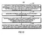
- FIG. 10 shows a flow diagram of a method 300 to provide a multiplied and temperature compensated synthesizer frequency output through the use of a temperature-dependent frequency multiplying element, in accordance with the present invention.
- This method 300 includes a first step 302 of providing a temperature dependent frequency oscillator and at least one frequency multiplication element in a locked loop circuit being programmed both to vary as a function of a temperature variation of the frequency oscillator and to vary as a function of a frequency multiplication factor.
- the frequency multiplication element provided is a multi-modulus divider and the locked loop circuit is a phase locked loop.
- a second step 304 includes measuring an ambient temperature in proximity to the oscillator and producing an ambient temperature value.
- a third step 306 includes searching a lookup table for a predetermined temperature dependent control signal corresponding to the ambient temperature value and the desired frequency multiplication factor. Alternatively, this step 306 may include calculating the temperature dependent control signal or a combination of searching and calculating the control signal.
- a last step 308 includes applying the control signal to the at least one frequency multiplication element such that a desired temperature compensated and multiplied output frequency is obtained from the synthesizer.
- Temperature compensation schemes often have the option of correcting for aging in the temperature-dependent frequency oscillator.
- a linear step size compensation is desirable for aging correction since the training of the temperature compensation is typically done before aging. If the step size of the compensation scheme is non-linear, the aging compensation cannot be added linearly to the temperature compensation. This situation requires the use of non-linear extrapolation circuitry to correctly compensate aging.
- the use of a noise-shaping digital modulator in the present invention provides additional linearity which is advantageous for use with aging compensation.
- N the integer smallest allowable change in frequency in this example occurs when the integer N changes by 1. This represents the smallest possible frequency resolution at F out .
- N the integer smallest possible frequency resolution at F out .
- the frequency change per single step in N changes at each extreme.
- the integral non-linearity for 500 equal steps of N, both up and down, is -6.8 ppm and +9.4 ppm. At the extremes of the desired ⁇ 50 ppm range this corresponds to an error of -14% and +19%, respectively.
- aging compensation using simple linear addition is substantially impossible when an accuracy of better than ⁇ 10 ppm is required.
- the present invention provides improved linear compensation performance by using a multi-modulus divider (shown as 222 in FIG. 8 ) controlled by a noise-shaping digital modulator, thereby reducing the complexity of aging compensation.
- the noise-shaping digital modulator used in the present invention provides a means of controlling the multi-modulus divider such that it can effectively provide a fractional, non-integer divide value such as N plus a fraction.
- the digital modulator does this by controlling the multi-modulus divider to divide by more than one value over a specified time interval. Over the specified time interval the effective divide value is a weighted average of the more than one divide values.
- the effective divide value of the divider is (N +1/100). This technique allows higher resolution with a small value of N.
- noise-shaping digital modulators have a fundamental frequency and noise sidebands about the fundamental frequency.
- Noise shaping in a digital modulator is a technique whereby the oversampled output of the digital modulator has its noise shaped in the frequency domain away from the fundamental frequency. This results in the invention having improved noise sidebands and a purer synthesized output frequency.
- the use of the noise-shaping digital modulator in the present invention reduces the complexity of aging compensation by providing a substantially linear operation of temperature compensation than is possible using only integer values for the multi-modulus divider. The substantially linear operation is described below for comparison with the foregoing integer-only operation.
- F out F osc ⁇ 1 + 1 N + Num / Den
- the smallest resolution possible with the dual-modulus divider comes with a numerator step of 1.
- the resolution is 0.099 ppm
- the resolution is 0.098 ppm
- the resolution is 0.100 ppm.
- the dual-modulus divider controlled by a fractional-division noise-shaping digital modulator gives a surprising result of a differential non-linearity of about ⁇ 1% which is much improved over the differential non-linearity of about ⁇ 30% resulting from the use of a fixed integer for N.
- the integral non-linearity of the invention is unexpectedly about ⁇ 0.5% which reduces error at the extremes of the desired ⁇ 50 ppm range to about 0.25 ppm. Therefore, the dual-modulus divider has the advantage of making aging compensation possible using simple linear addition when an accuracy of better than 0.5 ppm is required.
Description
- The present invention relates generally to frequency synthesizers used in conjunction with piezoelectric frequency oscillators in a multi-channel radio and, in particular, to a frequency synthesizer with temperature compensation and frequency multiplication and method of providing the same.
- Frequency synthesizers have typically been provided with reference frequency signals from crystal controlled frequency oscillators having temperature compensation circuits for use in frequency stabilized radio communications. These compensation circuits may be composed of analog or digital devices and are used to provide a relatively flat frequency output over temperature. Typically, a capacitive element is provided to allow absolute adjustment of the final frequency of the oscillator. This capacitive element is generally either in the form of a trim capacitor or an analog varactor controlled by an applied DC voltage. By adjusting this capacitance, the user is able to adjust (warp) the oscillator onto a desired final frequency.
- As should be recognized by those skilled in the prior art, the frequency adjustment range (warpability) of a crystal controlled frequency oscillator is limited by the physical size of the crystal and its electrodes. An increase in warpability necessitates the use of a crystal with an increased width-to-thickness ratio. However, an increase of width-to-thickness ratio causes a crystal to be more fragile and more costly than a crystal without a higher warpability requirement. Further, the long term stability of a highly warpable crystal is compromised due to its more sensitive nature.
- Warpability may also be increased by the use of a capacitive element having a larger tuning range. However, this typically requires that the element be of a physically larger size. Along with increasing the cost and size of the oscillator, the size of the element may bring other problems. In particular, analog varactors are necessarily large and do not scale as well with integrated circuit process shrinks as do digital circuits. Additionally, these reactive elements have their own variation with temperature, outside of the crystal temperature variation, which must be controlled by an applied voltage, as well as being compensated along with the crystal temperature variation. For good temperature performance of a varactor, a high supply voltage is needed for bias. However, this restricts the use of a lower voltage, single-supply operated frequency oscillator. Further, the oscillator AC voltage output swing must also be controlled to prevent the varactor from conducting.
- In typical frequency synthesizer applications, the frequency is manipulated three or more times. First, a crystal controlled frequency oscillator has temperature compensation circuitry applied to provide a relatively flat frequency output over temperature. Second, the oscillator is warped onto a desired frequency. Third, this corrected oscillator frequency is multiplied in a phase locked loop (PLL) to produce the higher frequencies required in local oscillators in radio communications equipment. It would be advantageous to temperature compensate a synthesizer output frequency with a single element without incorporating additional synthesizer elements.
- Yamashita K et al; "Frequency Stabilizing Method Using PSCL (Phase Slip-Controlled Loop)" 39th IEEE Vehicular Technology Conference, San Francisco, May 1-3,1989, vol. 1, 1 May 1989, pages 215-219, XP000076304 Institute of Electrical and Electronics Engineers discloses a circuit corresponding to circuit shown in
FIG. 4 of the present application and described herein in relation to that FIG. - There is a need for a temperature compensated frequency oscillator using a PLL frequency synthesizer which: achieves more accurate, linear and repeatable temperature compensation with more simplified circuitry; does not need tunable reactive elements to warp the oscillator onto the desired frequency thereby allowing smaller, less expensive elements to be used; provides a temperature-dependent frequency multiplying element whereby temperature compensation of the crystal oscillator and other circuit elements in the frequency synthesizer is achieved, In addition, it is desirable to provide a low cost, small sized, low current drain, high yield oscillator and PLL that allows control of the temperature compensation of the crystal oscillator and other circuit elements, warping, and frequency multiplication of the PLL without incurring any detrimental spurious frequency responses.
- In a first aspect, the present invention provides a frequency synthesizer with temperature compensation and frequency multiplication, as claimed in
claim 1. - In a further aspect, the present invention provides a method of temperature compensating and multiplying a frequency output in a frequency synthesizer, as claimed in claim 8.
-
-
FIG. 1 is a block diagram of a prior art circuit which provides a temperature compensated reference frequency signal to a temperature-independent frequency multiplier; -
FIG. 2 is a block diagram of a prior art circuit which provides pulse deletion circuitry to temperature compensate a temperature-dependent frequency signal which is then applied to a temperature-independent PLL; -
FIG. 3 is a block diagram of a prior art circuit which utilizes a direct digital synthesizer to temperature compensate a temperature-dependent frequency signal which is then applied to a temperature-independent PLL; -
FIG. 4 is a block diagram of a prior art circuit which provides a temperature compensating signal to a direct digital synthesizer (DDS) accumulator in a PLL to correct for a temperature-dependent frequency oscillator; -
FIG. 5 is a block diagram of a circuit which provides a temperature-dependent element coupled to a locked loop circuit used to temperature compensate a signal from a temperature-dependent frequency oscillator and to give the locked loop circuit a temperature-dependent multiplication factor, in accordance with the present invention; -
FIG. 6 is one embodiment of the circuit ofFIG. 5 wherein the locked loop circuit is a PLL and the temperature-dependent multiplication element is a multi-modulus frequency divider being fed by a noise-shaping digital modulator signal, in accordance with the present invention; -
FIG. 7 is a block diagram of a circuit which provides a multi-modulus frequency divider within a PLL to temperature compensate a temperature-dependent frequency oscillator signal which is applied to a PLL to provide a temperature-dependent multiplication factor, in accordance with the present invention; -
FIG. 8 is a preferred embodiment of the circuit ofFIG. 7 wherein an additional mixer in used to increase the resolution of the PLL, in accordance with the present invention; -
FIG. 9 is a block diagram of a circuit which provides a multi-modulus frequency divider and control circuitry to produce a temperature-dependent frequency signal which is mixed into a PLL loop at a VCO output to provide a temperature-dependent multiplication factor, in accordance with the present invention; and -
FIG. 10 is a flow diagram of a method to provide a multiplied and temperature compensated frequency output through the use of a temperature-dependent PLL element. -
FIG. 1 shows a priorart frequency source 10 providing a multiplied and temperature compensatedfrequency output 12. In this device a temperature compensatedfrequency oscillator 14 is coupled to a temperature-independent frequency multiplier 16 which provides the desiredfrequency output 12. - The
frequency oscillator 14 includes acrystal oscillator 18, at least onefrequency warp element 20 which is typically a varactor, atemperature compensation controller 22, atemperature sensor 24, and amemory 26. Thememory 26 contains a preprogrammed lookup table of temperature compensating data for the crystal that correspond to predetermined temperature varying voltage signals provided by thetemperature sensor 24. Typically, thesensor 24 is located in proximity to the crystal to reduce errors which may arise due to temperature gradients across thefrequency oscillator 14. Thesensor 24 provides atemperature indicating signal 28 to thecontroller 22 which directs thecontroller 22 to look-up the crystal compensation data in thememory 26 corresponding to thesensor signal 28. Thecontroller 22 then directs a correspondingadjustment voltage signal 30 to thewarp elements 20 to change their capacitance. Thewarp elements 20 are coupled to thefrequency oscillator circuit 18 such that a change in capacitance will cause a corresponding change in thefrequency output 32 of thefrequency oscillator 14. In this way, thefrequency oscillator 14 provides a relatively stable temperature compensatedfrequency output 32 to couple to thefrequency multiplier 16. Thefrequency oscillator 14 may also include an external DC voltage warp signal (not shown) to allow the adjustment of thefrequency oscillator 14 to aparticular output frequency 32. - The
frequency multiplier 16 is typically a frequency synthesizer incorporating a phase locked loop (PLL). PLL frequency synthesizers based on approaches such as fractional division or sigma-delta modulation are devices known in the art to realize temperature-independent frequency multiplication greater than one. Similarly, frequency dividers are devices known in the art to realize temperature-independent frequency multiplication less than one. Typically, thefrequency multiplier 16 takes the temperature compensatedfrequency output 32 from thefrequency oscillator 14 and multiplies it to output another, usually higher,frequency 12 for use as a local oscillator in radio communications equipment. - The disadvantage of this prior
art frequency source 10 is that multiple adjustments of frequency occur in the circuit, each adjustment requiring particular additional circuitry of its own. Thefrequency oscillator 14 requireswarp elements 20 to provide temperature compensation of the crystal, and thefrequency source 10 requires amultiplier circuit 16 to translate theoutput frequency 12. Thewarp elements 20 typically include large non-linear analog varactors which require a particular crystal design that is more sensitive to capacitive load changes. Further, the more sensitive crystal design also makes the crystal more sensitive to temperature variations and aging. In addition, the temperature variations of the other components in the frequency source are not compensated. -
FIG. 2 shows another priorart frequency source 50 that utilizes afrequency oscillator 52 that is allowed to vary frequency over temperature. In thissource 50, theoscillator output 54 is temperature dependent, but is subsequently compensated by apulse deletion circuit 56 to provide temperature correction of theoutput 54 before being coupled to aPLL 58. ThePLL 58 includes afirst divider 60, asecond divider 62, aphase detector 64, a low-pass loop filter 66, and a voltage controlled oscillator (VCO) 68. Also, the source includes a temperaturecompensation control circuit 72 for controlling thepulse deletion circuit 56. - The
output 54 of thefrequency oscillator 52 is a temperature-varying square wave pulse train which is coupled through thepulse deletion circuitry 56 to thePLL 58. Thecontrol circuit 72 directs thepulse deletion circuitry 56 to delete pulses from the pulse train to lower the frequency in accordance with temperature variations of thefrequency oscillator 52. In this way, a relatively stable temperature compensatedfrequency output 76 is coupled to thePLL 58. - The output from the
pulse deletion circuitry 76 is frequency divided by thefirst divider 60 and input to aphase detector 64 as a reference signal. An output from theVCO 68 for outputting a desired frequency is divided by thesecond divider 62 and input into thephase detector 64. Thephase detector 64 outputs aphase difference signal 78 through theloop filter 66 to acontrol terminal 80 of theVCO 68. Theloop filter 66 reduces switching transients generated in thephase detector 64 by missing pulses in the pulse train. - The disadvantage of this prior
art frequency source 50 is that pulse deletion forces thephase detector 64 to generate a longphase difference signal 78 to theVCO 68 over any time period where a pulse is missing. This switching between long and short phase difference signals 78 generates sideband signals in theVCO 68 which may cause radio communication transceivers to receive or transmit on an incorrect frequency. This necessitates the use of a very low frequency low-pass loop filter 66 which requires large filter components and causes slow lock times. For example, a 1 ppm correction in a 15 MHz reference signal requires the deletion of 15 pulse/second from the pulse train, which causes 15 Hz phase difference signals 78 at theloop filter 66. Theloop filter 66 needs to reject the 15 Hzsignals 78 to be effective. A 15 Hz filter typically requires large components which is a disadvantage. -
FIG. 3 shows another priorart frequency source 100 that has very similar circuitry to the source ofFIG. 2 , but utilizes a direct digital synthesizer (DDS) 102 in place of the pulse deletion circuit ofFIG. 2 . TheDDS 102 is clocked by the signal from the temperature-dependent frequency oscillator 104, amicro-controller 106 performs a temperature compensating bit correction, and a D-A converter in theDDS 102 converts the correcteddata 108 into an temperature compensatedfrequency output 110. Thissource 100 has the advantage of generating a regular pulse train which reduces sideband signals, but at the expense of large current drain in the D-A converter. Further, thissource 100 has the disadvantage of requiring additionalfrequency multiplication elements 112 in the circuit to obtain a desired multiplied output, and the temperature variations of the other components in the source are not compensated. -
FIG. 4 shows another priorart frequency source 150 that utilizes aDDS accumulator 152 to provide temperature compensation of a frequency oscillator 156 and to achieve fine frequency resolution. Thissource 150 has the disadvantage of poor spurious performance at anoutput 154 of theaccumulator 152 due to the use of a single accumulator which takes its output from the high bit of an accumulator register. It should be recognized that accumulators are well known in the art. This approach requires significant filtering similar to that required by thepulse deletion circuit 56 ofFIG. 2 . -
FIG. 5 shows a general implementation of afrequency synthesizer 200 in accordance with the present invention. Asignal 204 from an uncompensated, temperature-dependentreference frequency oscillator 202 is input to a lockedloop circuit 206 which contains a temperature-dependentfrequency multiplying element 208. The lockedloop circuit 206 may be a phase locked loop, a frequency locked loop. In particular, a phase locked loop circuit would include a phase detector, a frequency locked loop circuit would include a frequency detector. In one embodiment, the lockedloop circuit 206 is a phase locked loop and theelement 208 is a multi-modulus divider, preferably adjusted by a noise shaping digital modulator to permit fractional division of a frequency, allowing finer resolution than integer dividers. - In a preferred embodiment, the
element 208 is a dual-modulus divider and is varied, dependent upon temperature, to temperature compensate thefrequency oscillator 202. This is achieved by a temperaturecompensation control circuit 210 which applies a temperature-dependent control signal 212 to theelement 208. Theelement 208 is used, not only to temperature compensate thefrequency oscillator 202, but also to multiply the oscillator frequency and provide frequency synthesis. Theelement 208 may also be used to temperature compensate all of the components of thefrequency synthesizer circuit 200. This is advantageous over the prior art where temperature-dependent components are independently temperature compensated. The use of a singletemperature compensating element 208, provides a great simplification over prior art synthesizers, in addition to the corresponding lower cost and lower current drain. - The present invention provides another advantage in that the frequency oscillator is no longer required to provide a crystal with a particular sensitivity. This is because the crystal oscillator does not need an expansive warp range to be warped onto a nominal frequency. This frequency adjustment function can now be performed in conjunction with the multiplying function of the
element 208. Therefore, a less sensitive and more robust crystal can be used which lowers cost. Also, a less sensitive crystal has better long term stability (aging). In addition, there is no longer a need for large tunable reactive elements such as varactors to warp the oscillator onto a desired frequency. -
FIG. 6 shows one embodiment of the present invention including a temperaturedependent frequency oscillator 202, a lockedloop circuit 206, shown as a PLL, a noise-shapingdigital modulator 214, and a temperaturecompensation control circuit 210. The lockedloop circuit 206 includes aphase detector 216 having an output coupled to aloop filter 218 having an output coupled to a voltage controlledoscillator 220 having an output coupled back through amulti-modulus divider 222 in afeedback path 240 of the lockedloop circuit 206 to a first input of thephase detector 216. Thefrequency oscillator 202 applies a frequency to a second input of thephase detector 216 through asignal path 242. Preferably, the oscillator provides a frequency signal through a temperature-independentsecond divider 224 which improves flexibility infrequency output 238 selection. Thecontrol circuit 210 includes a temperature·sensor 226 and amemory 230 being coupled to a temperature compensation controller 228, the controller 228 -of thecontrol circuit 210 being coupled to thedivider 222 and for controlling thedivider 222. - The temperature
compensation control circuit 210 monitors atemperature signal 232 from a connectingtemperature sensor 226 and uses thetemperature signal 232 to look up a value corresponding to thetemperature signal 232 in a connectingmemory 230. Thememory 230 is stored with values predetermined from previous temperature training of the synthesizer. The values have been computed to compensate for output frequency errors produced as the elements of the synthesizer circuit are subjected to varying temperature. The temperature compensating procedure can use a lookup table, a calculation or a combination of the two equally well for determining the appropriate temperature compensating value. As thesensor 226 indicates a change in ambient temperature, thememory 230 supplies the appropriatecorresponding compensation value 234 to the temperature compensation controller 228. The controller 228 produces an appropriate temperature-dependentmodulator control signal 212 along with a desired PLL multiplication factor to thedivider 222. In a preferred embodiment, thecontrol signal 212 is applied through a noise-shapingdigital modulator 214 such that a noise reducing temperature-dependent dividermodulus control signal 236 is applied to thedivider 222 whereby a multiplied and temperature compensated frequency synthesizer output is achieved. - This is different from the prior art (as shown in
FIG. 1 ) where separate synthesizer elements such as the reference frequency oscillator are independently temperature compensated. Also, in the case of the prior art oscillator, frequency warp elements are used to provide temperature compensation which does not include temperature compensation of all the elements of a synthesizer. The present invention has the advantage of supplying all temperature compensation and frequency multiplication in a single temperature compensating element without the use of additional frequency warp elements. - In a preferred embodiment, a noise-shaping
digital modulator 214 is connected in thecontrol signal path 212 from the controller 228 to themulti-modulus divider 222 to control thedivider 222 such that the PLL can achieve good frequency resolution while reducing spurious frequencies. The output of the noise-shapingmodulator 214 is made temperature dependent by the temperaturecompensation control circuit 210. Themodulator 214 increments and decrements the modulus of themulti-modulus divider 222 over a particular time period such that an averaged fractional modulus is obtained. It should be recognized that faster switching provides a better averaged modulus. Further, themodulator 214 varies the frequency division factor of themulti-modulus divider 222 as a function of temperature through the temperature-dependentdivider modulus control 236 such that a multiplied and temperature compensatedsynthesizer frequency output 238 is obtained. - The noise-shaping
digital modulator 214 can be implemented in various ways. Known implementations of digital modulators in the prior art are fractional-division and sigma-delta modulators, both of which can provide adequate noise-shaping of their outputs. A sigma-delta modulator with a one bit output achieves fine resolution of the divider and therefore fine resolution of the synthesizer frequency output. These modulators serve to create an average divider modulus by varying the divider modulus in such a manner as to shape the noise created as the divider modulus is varied and translate the noise away from a nominal output frequency of the divider. -
FIG. 7 shows an alternative embodiment of the synthesizer ofFIG. 6 where the temperature dependentmulti-modulus divider 222 is placed in thesignal path 242 of theoscillator 202 and the temperatureindependent divider 224 is place in thefeedback path 240 of the lockedloop circuit 206 which is preferably a PLL. It should be recognized that any or all of the dividers in the synthesizer may be controlled with a temperature-dependent signal, but unless the system performance warrants the additional complexity this would be redundant, inefficient and not cost effective. -
FIG. 8 shows an alternative embodiment of the synthesizer ofFIG. 7 where amixer 244 is connected in thefeedback path 240 and coupled to a feed forward path connecting from theoscillator signal path 242. The additional of themixer 244 is used to increase the resolution of the lockedloop circuit 206. -
FIG. 9 shows another embodiment of the present invention where a third temperatureindependent divider 246 is connected in a feed forward path connecting from theoscillator signal path 242, and a temperatureindependent divider 224 is connected in thefeedback path 240 of the lockedloop circuit 206 which is preferably a PLL. Amixer 248 is connected in thefeedback path 240 and is coupled to thesignal path 242 through amulti-modulus divider 222. It should be recognized that various other locked loop configurations are possible using a temperature dependentmulti-modulus divider 222. For example, the synthesizer may include more than one each of a feedback path, an oscillator signal path and a feed forward path depending on the resolution or complexity required. In addition, multiple independent locked loop circuits may be controlled in parallel with a control circuit, the independent locked loop signals being combined by a mixer to provide improved resolution. Any or all of these paths may incorporated a temperature dependent multi-modulus divider controlling both temperature compensation and frequency multiplication. -
FIG. 10 shows a flow diagram of amethod 300 to provide a multiplied and temperature compensated synthesizer frequency output through the use of a temperature-dependent frequency multiplying element, in accordance with the present invention. Thismethod 300 includes afirst step 302 of providing a temperature dependent frequency oscillator and at least one frequency multiplication element in a locked loop circuit being programmed both to vary as a function of a temperature variation of the frequency oscillator and to vary as a function of a frequency multiplication factor. In a preferred embodiment, the frequency multiplication element provided is a multi-modulus divider and the locked loop circuit is a phase locked loop. - A
second step 304 includes measuring an ambient temperature in proximity to the oscillator and producing an ambient temperature value. Athird step 306 includes searching a lookup table for a predetermined temperature dependent control signal corresponding to the ambient temperature value and the desired frequency multiplication factor. Alternatively, thisstep 306 may include calculating the temperature dependent control signal or a combination of searching and calculating the control signal. Alast step 308 includes applying the control signal to the at least one frequency multiplication element such that a desired temperature compensated and multiplied output frequency is obtained from the synthesizer. - Temperature compensation schemes often have the option of correcting for aging in the temperature-dependent frequency oscillator. A linear step size compensation is desirable for aging correction since the training of the temperature compensation is typically done before aging. If the step size of the compensation scheme is non-linear, the aging compensation cannot be added linearly to the temperature compensation. This situation requires the use of non-linear extrapolation circuitry to correctly compensate aging. The use of a noise-shaping digital modulator in the present invention provides additional linearity which is advantageous for use with aging compensation.
- The linearity advantage of using a noise-shaping digital modulator in the present invention can be shown by example, with reference to the invention of
FIG. 8 . First, let themulti-modulus divider 222 be controlled by other than a noise-shaping digital modulator. This means that N is a fixed integer value at a given temperature. Let Fout be the multiplied and temperature-compensated output frequency and let Fosc be the frequency of the temperature dependent frequency oscillator. For asecond divider 224 value of M=1:
- The change in the multiplied and temperature-compensated output frequency, Fout, with respect to a change in N is:

- When normalized to Fosc this equation becomes:

- The smallest allowable change in frequency in this example occurs when the integer N changes by 1. This represents the smallest possible frequency resolution at Fout. In order to change a frequency at Fout by 0.1 ppm using only one step in N, it is necessary that N be about 3200, as follows:
- For

- To change frequency by 50 ppm N should range from about 2730 to about 3756 as follows:


- However, the frequency change per single step in N changes at each extreme. At N=2730, the frequency change per step is:

which equals a resolution of 0.134 ppm. At the nominal N=3162 the resolution is 0.100 ppm, while at N=3756 the resolution is 0.071 ppm. Therefore, using an integer divider with a nominal 0.1 ppm frequency resolution results in a differential non-linearity of about ±30%. - An attempt to adjust frequency ±50 ppm using the given frequency resolution at N=3162, 0.100 ppm, will produce serious errors. For example, in a linear system ±500 steps (50 ppm/0.100 ppm/step) would be needed to achieve ±50 ppm frequency adjustment. However, due to the non-linearity of frequency resolution, the following frequency changes result;


- The integral non-linearity for 500 equal steps of N, both up and down, is -6.8 ppm and +9.4 ppm. At the extremes of the desired ±50 ppm range this corresponds to an error of -14% and +19%, respectively. For the invention of
FIG. 8 , when only integer steps are used in the multi-modulus divider, aging compensation using simple linear addition is substantially impossible when an accuracy of better than ±10 ppm is required. - The present invention provides improved linear compensation performance by using a multi-modulus divider (shown as 222 in
FIG. 8 ) controlled by a noise-shaping digital modulator, thereby reducing the complexity of aging compensation. The noise-shaping digital modulator used in the present invention provides a means of controlling the multi-modulus divider such that it can effectively provide a fractional, non-integer divide value such as N plus a fraction. The digital modulator does this by controlling the multi-modulus divider to divide by more than one value over a specified time interval. Over the specified time interval the effective divide value is a weighted average of the more than one divide values. For example, if the multi-modulus divider is controlled to divide by N for 99% of the time interval and N+1 for 1% of the time interval, the effective divide value of the divider is (N +1/100). This technique allows higher resolution with a small value of N. - The output frequencies of noise-shaping digital modulators have a fundamental frequency and noise sidebands about the fundamental frequency. Noise shaping in a digital modulator is a technique whereby the oversampled output of the digital modulator has its noise shaped in the frequency domain away from the fundamental frequency. This results in the invention having improved noise sidebands and a purer synthesized output frequency. The use of the noise-shaping digital modulator in the present invention reduces the complexity of aging compensation by providing a substantially linear operation of temperature compensation than is possible using only integer values for the multi-modulus divider. The substantially linear operation is described below for comparison with the foregoing integer-only operation.
- In a preferred embodiment, the present invention, as shown in
FIG. 8 for example, to satisfy the same 0.1 ppm step size requirement and ±50 ppm range, uses a dual-modulus divider of value N=100/101 in conjunction with a fractional-N step size of Num/Den (numerator/denominator). More preferably, a fractional-division noise-shaping modulator is connected in the control signal path of the dual-modulus divider. The noise-shaping modulator uses accumulator lengths of Den=1000 with Num varying from 0 to 1000. With reference toFIG. 8 ;
- The resulting change in temperature-compensated output frequency, Fout, with respect to a fractional change in the effective N for a dual-modulus divider due to a change in Num is:

- The smallest resolution possible with the dual-modulus divider comes with a numerator step of 1. At a nominal Num/Den=500/1000 the resolution is 0.099 ppm, while at Num/Den=1000/1000 the resolution is 0.098 ppm and at Num/Den=0/1000 the resolution is 0.100 ppm. In this example, the dual-modulus divider controlled by a fractional-division noise-shaping digital modulator gives a surprising result of a differential non-linearity of about ±1% which is much improved over the differential non-linearity of about ±30% resulting from the use of a fixed integer for N. In addition, the integral non-linearity of the invention is unexpectedly about ±0.5% which reduces error at the extremes of the desired ±50 ppm range to about 0.25 ppm. Therefore, the dual-modulus divider has the advantage of making aging compensation possible using simple linear addition when an accuracy of better than 0.5 ppm is required.
- Although various embodiments of this invention have been shown and described, it should be understood that various modifications and substitutions, as well as rearrangements and combinations of the preceding embodiments, can be made by those skilled in the art, without departing from the novel scope of this invention.
Claims (8)
- A frequency synthesizer with temperature compensation and frequency multiplication, comprising:a temperature dependent frequency oscillator (202);at least one locked loop circuit (206) coupled to the oscillator (202) and chosen from the group consisting of a phase locked loop and a frequency locked loop;at least one frequency division element (208, 222) in or coupled to the locked loop circuit, the element programmed to vary as a function of a temperature variation of the frequency oscillator (202) and to vary as a function of a frequency multiplication factor, wherein the at least one frequency division element is a multi-modulus divider;a control circuit (210) including a temperature sensor (226) coupled to a temperature compensation controller (228), the controller is configured to provide a temperature-dependent modulator control signal based on a temperature measured by the temperature sensor;a noise-shaping digital modulator (214) connected to the control circuit and the at least one division element (208, 222), the noise-shaping digital modulator in a control signal path of the control circuit (210) and responsive to the temperature-dependent modulator control signal provided by the controller to generate a temperature dependent divider control input to the at least one division element, the noise-shaping digital modulator being configured to vary the modulus of the at least one division element as a function of temperature by varying the temperature dependent divider control input so as to temperature compensate the frequency oscillator, wherein the noise-shaping digital modulator is configured to create an average divider modulus by varying the modulus in such a manner as to shape noise created as the modulus is varied ; andthe oscillator (202), noise-shaping digital modulator (214) and the at least one division element (208, 222) being coupled such that a temperature independent multiplied frequency synthesizer output (238) is provided.
- The frequency synthesizer of claim 1, wherein the at least one frequency division element (208, 222) is a dual-modulus divider.
- The frequency synthesizer of claim 2, wherein the at least one frequency division element (222) is connected in at least one of a feedback path (240) of the loop circuit (206) and a signal path (242) between the oscillator (202) and the loop circuit (206).
- The frequency synthesizer of claim 3, further comprising at least one mixer (244), the at least one mixer (244) being coupled to the at least one feedback path (240), and wherein the at least one frequency division element (222) is connected in an electrical path selected from one of the group of at least one signal path between the oscillator and the at least one mixer, the at least one feedback path of the phase locked loop and the at least one signal path between the oscillator and the loop circuit (206).
- The frequency synthesizer of claim 1, wherein the at least one frequency division element (222) is programmed to obtain an averaged fractional modulus.
- The frequency synthesizer of claim 1, wherein the locked loop circuit (206) includes an associated detector (216) being coupled to a loop filter (218) which is coupled to a voltage controlled oscillator (220) having an output coupled back to a first input of the detector (216) through the element (222), the oscillator (202) being coupled to a second input of the detector (216).
- The frequency synthesizer of claim 1, further comprising at least one mixer (244), the at least one mixer (244) being coupled to the at least one feedback path (240), and wherein the at least one frequency division element (222) is connected in at least one signal path between the oscillator and the at least one mixer.
- A method of temperature compensating and multiplying a frequency output in a frequency synthesizer, comprising the steps of:providing (302) a temperature dependent frequency oscillator coupled to at least one frequency division element being programmed to vary as a function of a temperature variation of the frequency oscillator and to vary as a function of a frequency multiplication factor, the frequency division element being connected to a noise-shaping digital modulator and being in or coupled to at least one locked loop circuit selected from the group consisting of a phase locked loop, and a frequency locked loop, wherein the frequency division element is a multi-modulus divider, wherein the noise-shaping digital modulator is configured to create an average divider modulus by varying the modulus in such a manner as to shape noise created as the modulus is varied;measuring (304) an ambient temperature value in proximity to the oscillator;searching (306) a lookup table for a predetermined temperature dependent modulator control signal corresponding to the ambient temperature value and the frequency multiplication factor; andapplying (308) the modulator control signal to the noise-shaping digital modulator to generate a temperature dependent divider control applied to the at least one frequency division element, the temperature dependent divider control varying the Modulus of the at least one division element as a function of temperature such that a desired temperature compensated and multiplied output frequency is obtained from the synthesizer.
Applications Claiming Priority (3)
| Application Number | Priority Date | Filing Date | Title |
|---|---|---|---|
| US635487 | 1996-04-22 | ||
| US08/635,487 US5604468A (en) | 1996-04-22 | 1996-04-22 | Frequency synthesizer with temperature compensation and frequency multiplication and method of providing the same |
| PCT/US1997/001824 WO1997040580A1 (en) | 1996-04-22 | 1997-01-31 | Frequency synthesizer with temperature compensation and frequency multiplication and method of providing the same |
Publications (3)
| Publication Number | Publication Date |
|---|---|
| EP0897616A1 EP0897616A1 (en) | 1999-02-24 |
| EP0897616A4 EP0897616A4 (en) | 1999-07-07 |
| EP0897616B1 true EP0897616B1 (en) | 2014-04-23 |
Family
ID=24547989
Family Applications (1)
| Application Number | Title | Priority Date | Filing Date |
|---|---|---|---|
| EP97904231.4A Expired - Lifetime EP0897616B1 (en) | 1996-04-22 | 1997-01-31 | Frequency synthesizer with temperature compensation and frequency multiplication and method of providing the same |
Country Status (6)
| Country | Link |
|---|---|
| US (1) | US5604468A (en) |
| EP (1) | EP0897616B1 (en) |
| JP (1) | JP2000509219A (en) |
| KR (1) | KR100292965B1 (en) |
| CN (1) | CN1161882C (en) |
| WO (1) | WO1997040580A1 (en) |
Families Citing this family (124)
| Publication number | Priority date | Publication date | Assignee | Title |
|---|---|---|---|---|
| US7525392B2 (en) * | 2006-08-05 | 2009-04-28 | Tang System | XtalClkChip: trimming-free crystal-free precision reference clock oscillator IC chip |
| US5848355A (en) * | 1993-07-07 | 1998-12-08 | Motorola, Inc. | Frequency synthesizer correction using a temperature responsive divisor control |
| US5781073A (en) * | 1996-07-24 | 1998-07-14 | Mii; Adam | Temperature compensation method for an output frequency drift of an oscillator |
| US5883844A (en) * | 1997-05-23 | 1999-03-16 | Stmicroelectronics, Inc. | Method of stress testing integrated circuit having memory and integrated circuit having stress tester for memory thereof |
| US5856766A (en) * | 1997-06-30 | 1999-01-05 | Motorola Inc. | Communication device with a frequency compensating synthesizer and method of providing same |
| US6282247B1 (en) * | 1997-09-12 | 2001-08-28 | Ericsson Inc. | Method and apparatus for digital compensation of radio distortion over a wide range of temperatures |
| JP3419274B2 (en) * | 1997-10-03 | 2003-06-23 | 富士電機株式会社 | Sensor output compensation circuit |
| JP3717289B2 (en) * | 1997-10-20 | 2005-11-16 | 富士通株式会社 | Integrated circuit device |
| US6400930B1 (en) * | 1998-11-06 | 2002-06-04 | Dspc Israel, Ltd. | Frequency tuning for radio transceivers |
| US6278867B1 (en) * | 1998-11-25 | 2001-08-21 | Ericsson Inc. | Methods and systems for frequency generation for wireless devices |
| KR100303781B1 (en) | 1998-12-30 | 2001-09-24 | 박종섭 | DL Clock Generator with Unlock Compensation Circuit for Solving Unlock Problems in Register-Controlled Digital DLs |
| US6321074B1 (en) * | 1999-02-18 | 2001-11-20 | Itron, Inc. | Apparatus and method for reducing oscillator frequency pulling during AM modulation |
| US6690215B2 (en) * | 1999-03-17 | 2004-02-10 | Tropian, Inc. | Sigma-delta-based frequency synthesis |
| US7072415B2 (en) * | 1999-10-19 | 2006-07-04 | Rambus Inc. | Method and apparatus for generating multi-level reference voltage in systems using equalization or crosstalk cancellation |
| US6396329B1 (en) * | 1999-10-19 | 2002-05-28 | Rambus, Inc | Method and apparatus for receiving high speed signals with low latency |
| US7124221B1 (en) | 1999-10-19 | 2006-10-17 | Rambus Inc. | Low latency multi-level communication interface |
| US7161513B2 (en) * | 1999-10-19 | 2007-01-09 | Rambus Inc. | Apparatus and method for improving resolution of a current mode driver |
| CA2288495A1 (en) * | 1999-11-02 | 2001-05-02 | Seste Dell'aera | Radio calibration by correcting the crystal frequency |
| US6396355B1 (en) * | 2000-04-12 | 2002-05-28 | Rockwell Collins, Inc. | Signal generator having fine resolution and low phase noise |
| US6928275B1 (en) * | 2000-05-08 | 2005-08-09 | Qualcomm Incorporated | Method and apparatus for compensating local oscillator frequency error |
| US6522871B1 (en) * | 2000-05-09 | 2003-02-18 | Qualcomm, Incorporated | Method and apparatus for compensating local oscillator frequency error through environmental control |
| EP1168634B1 (en) * | 2000-06-28 | 2007-06-13 | STMicroelectronics N.V. | Method for reducing the electricity consumption of a mobile cellular telephone |
| US6420938B1 (en) | 2000-08-30 | 2002-07-16 | Lawrence Hoff | Software controlled crystal oscillator |
| FI109626B (en) * | 2000-11-08 | 2002-09-13 | Nokia Corp | Synthesizer arrangement and method for generating signals, in particular for multimode radiotelephone equipment |
| US6456164B1 (en) | 2001-03-05 | 2002-09-24 | Koninklijke Philips Electronics N.V. | Sigma delta fractional-N frequency divider with improved noise and spur performance |
| WO2002082656A2 (en) * | 2001-04-09 | 2002-10-17 | Cts Corporation | High frequency vcxo structure |
| US6946919B2 (en) * | 2002-01-14 | 2005-09-20 | Cts Corporation | Controllable crystal oscillator component |
| US20030007585A1 (en) * | 2001-06-28 | 2003-01-09 | Dalton Declan M. | Fractional-n frequency synthesizer |
| JP3869699B2 (en) * | 2001-10-24 | 2007-01-17 | 株式会社アドバンテスト | Timing generator, semiconductor test apparatus, and timing generation method |
| JP3973910B2 (en) * | 2002-01-21 | 2007-09-12 | シチズンホールディングス株式会社 | Method for manufacturing temperature compensated oscillator |
| US7546097B2 (en) * | 2002-03-06 | 2009-06-09 | Qualcomm Incorporated | Calibration techniques for frequency synthesizers |
| US6946884B2 (en) | 2002-04-25 | 2005-09-20 | Agere Systems Inc. | Fractional-N baseband frequency synthesizer in bluetooth applications |
| US7292629B2 (en) * | 2002-07-12 | 2007-11-06 | Rambus Inc. | Selectable-tap equalizer |
| US8861667B1 (en) | 2002-07-12 | 2014-10-14 | Rambus Inc. | Clock data recovery circuit with equalizer clock calibration |
| US7362800B1 (en) | 2002-07-12 | 2008-04-22 | Rambus Inc. | Auto-configured equalizer |
| US7791424B2 (en) * | 2002-10-15 | 2010-09-07 | Marvell World Trade Ltd. | Crystal oscillator emulator |
| US7760039B2 (en) * | 2002-10-15 | 2010-07-20 | Marvell World Trade Ltd. | Crystal oscillator emulator |
| US20060113639A1 (en) * | 2002-10-15 | 2006-06-01 | Sehat Sutardja | Integrated circuit including silicon wafer with annealed glass paste |
| US7768360B2 (en) * | 2002-10-15 | 2010-08-03 | Marvell World Trade Ltd. | Crystal oscillator emulator |
| US20060262623A1 (en) | 2002-10-15 | 2006-11-23 | Sehat Sutardja | Phase locked loop with temperature compensation |
| US6831491B2 (en) * | 2002-12-23 | 2004-12-14 | Agilent Technologies, Inc. | Systems and methods for correcting phase locked loop tracking error using feed-forward phase modulation |
| US7003274B1 (en) * | 2003-03-05 | 2006-02-21 | Cisco Systems Wireless Networking (Australia) Pty Limited | Frequency synthesizer and synthesis method for generating a multiband local oscillator signal |
| US7315601B2 (en) * | 2003-03-13 | 2008-01-01 | Texas Instruments Incorporated | Low-noise sigma-delta frequency synthesizer |
| US7064617B2 (en) * | 2003-05-02 | 2006-06-20 | Silicon Laboratories Inc. | Method and apparatus for temperature compensation |
| US20050068118A1 (en) * | 2003-09-30 | 2005-03-31 | Silicon Laboratories, Inc. | Reconfigurable terminal |
| US7295077B2 (en) * | 2003-05-02 | 2007-11-13 | Silicon Laboratories Inc. | Multi-frequency clock synthesizer |
| US7436227B2 (en) * | 2003-05-02 | 2008-10-14 | Silicon Laboratories Inc. | Dual loop architecture useful for a programmable clock source and clock multiplier applications |
| US7288998B2 (en) * | 2003-05-02 | 2007-10-30 | Silicon Laboratories Inc. | Voltage controlled clock synthesizer |
| US7187241B2 (en) * | 2003-05-02 | 2007-03-06 | Silicon Laboratories Inc. | Calibration of oscillator devices |
| EP1623503B1 (en) * | 2003-05-02 | 2012-03-14 | Silicon Laboratories, Inc. | Method and apparatus for a low jitter dual-loop fractional -n synthesizer |
| US20050036580A1 (en) * | 2003-08-12 | 2005-02-17 | Rana Ram Singh | Programmable phase-locked loop fractional-N frequency synthesizer |
| US7167058B2 (en) * | 2003-12-11 | 2007-01-23 | Seiko Epson Corporation | Temperature compensation for a variable frequency oscillator without reducing pull range |
| US7161440B2 (en) * | 2003-12-11 | 2007-01-09 | Seiko Epson Corporation | Temperature compensation circuit |
| US6995622B2 (en) * | 2004-01-09 | 2006-02-07 | Robert Bosh Gmbh | Frequency and/or phase compensated microelectromechanical oscillator |
| JP4094576B2 (en) * | 2004-03-26 | 2008-06-04 | エルピーダメモリ株式会社 | Oscillator circuit |
| EP1762004B1 (en) | 2004-06-24 | 2011-01-05 | Nokia Siemens Networks Oy | Frequency synthesizer |
| US7068110B2 (en) * | 2004-06-28 | 2006-06-27 | Silicon Laboratories Inc. | Phase error cancellation |
| US7253671B2 (en) * | 2004-06-28 | 2007-08-07 | Intelliserv, Inc. | Apparatus and method for compensating for clock drift in downhole drilling components |
| KR100584602B1 (en) * | 2004-07-20 | 2006-05-30 | 삼성전자주식회사 | Apparatus and method for setting a ring oscillator responding to environmental change of an image forming apparatus |
| US20060095221A1 (en) * | 2004-11-03 | 2006-05-04 | Teradyne, Inc. | Method and apparatus for controlling variable delays in electronic circuitry |
| US7327172B2 (en) * | 2005-06-27 | 2008-02-05 | Lsi Corporation | Integrated clock generator with programmable spread spectrum using standard PLL circuitry |
| WO2007000712A1 (en) * | 2005-06-29 | 2007-01-04 | Nxp B.V. | Synchronization scheme with adaptive reference frequency correction |
| US7539277B2 (en) * | 2005-09-09 | 2009-05-26 | Freescale Semiconductor, Inc. | Binary stream switching controlled modulus divider for fractional frequency synthesis |
| US20070057737A1 (en) * | 2005-09-14 | 2007-03-15 | Freescale Semiconductor, Inc. | Compensation for modulation distortion |
| CN100547905C (en) * | 2005-11-17 | 2009-10-07 | 中国科学院半导体研究所 | Circulation circuit voltage-controlled oscillator with temperature compensation effect |
| US7541883B2 (en) * | 2005-11-17 | 2009-06-02 | Cts Corporation | Coaxial resonator based voltage controlled oscillator/phased locked loop synthesizer module |
| US7482885B2 (en) * | 2005-12-29 | 2009-01-27 | Orca Systems, Inc. | Method of frequency synthesis for fast switching |
| JP4487937B2 (en) * | 2006-01-17 | 2010-06-23 | 株式会社デンソー | Microcomputer |
| JP4459911B2 (en) * | 2006-02-08 | 2010-04-28 | 富士通株式会社 | DPLL circuit with holdover function |
| US7519349B2 (en) * | 2006-02-17 | 2009-04-14 | Orca Systems, Inc. | Transceiver development in VHF/UHF/GSM/GPS/bluetooth/cordless telephones |
| JP2007243586A (en) * | 2006-03-08 | 2007-09-20 | Oki Electric Ind Co Ltd | Circuit and method for correcting clock, mobile body terminal, and base station device |
| US7742785B2 (en) * | 2006-08-09 | 2010-06-22 | Qualcomm Incorporated | Reference signal generation for multiple communication systems |
| US7649426B2 (en) * | 2006-09-12 | 2010-01-19 | Cts Corporation | Apparatus and method for temperature compensation of crystal oscillators |
| TWI424680B (en) * | 2006-10-17 | 2014-01-21 | Marvell World Trade Ltd | Crystal oscillator emulator |
| WO2008048644A2 (en) * | 2006-10-17 | 2008-04-24 | Marvell World Trade Ltd. | Crystal oscillator emulator |
| KR100895029B1 (en) | 2007-01-17 | 2009-04-24 | 노키아 코포레이션 | Frequency synthesizer |
| KR100861966B1 (en) * | 2007-02-02 | 2008-10-07 | 엘아이지넥스원 주식회사 | Apparatus for stability of yig osc in pll |
| JP4656103B2 (en) * | 2007-07-31 | 2011-03-23 | パナソニック株式会社 | Oscillator, and receiver and electronic apparatus using the same |
| US7545228B1 (en) * | 2007-09-12 | 2009-06-09 | Sitime Inc. | Dynamic temperature compensation for a digitally controlled oscillator using dual MEMS resonators |
| US8094022B2 (en) * | 2007-09-25 | 2012-01-10 | Infinid Technologies, Inc | Active ID tags for increased range and functionality |
| GB2455717A (en) * | 2007-12-17 | 2009-06-24 | Ubiquisys Ltd | Frequency synthesis in a wireless basestation |
| JP4835596B2 (en) * | 2008-01-10 | 2011-12-14 | パナソニック株式会社 | Synthesizer or oscillator module, and synthesizer module, receiver, and electronic device using the synthesizer |
| JP4811417B2 (en) * | 2008-02-14 | 2011-11-09 | パナソニック株式会社 | Receiving device and electronic device |
| JP4524326B2 (en) * | 2008-05-13 | 2010-08-18 | 日本電波工業株式会社 | Crystal oscillator |
| CN101272142B (en) * | 2008-05-20 | 2011-05-18 | 曹秀娟 | Frequency synthesizer |
| WO2010023883A1 (en) * | 2008-08-28 | 2010-03-04 | パナソニック株式会社 | Synthesizer and reception device and electronic device using the same |
| US7764131B1 (en) | 2008-09-23 | 2010-07-27 | Silicon Labs Sc, Inc. | Precision, temperature stable clock using a frequency-control circuit and dual oscillators |
| US7830216B1 (en) * | 2008-09-23 | 2010-11-09 | Silicon Labs Sc, Inc. | Precision, temperature stable clock using a frequency-control circuit and a single oscillator |
| US7812682B2 (en) * | 2009-03-05 | 2010-10-12 | Nel Frequency Controls, Inc. | Crystal-based oscillator for use in synchronized system |
| US8072273B2 (en) * | 2009-03-05 | 2011-12-06 | Nel Frequency Controls, Inc. | System employing synchronized crystal oscillator-based clock, to be used in either discrete or integrated applications |
| JP5424473B2 (en) * | 2009-08-31 | 2014-02-26 | 京セラクリスタルデバイス株式会社 | Oscillator circuit |
| JP5426316B2 (en) * | 2009-10-21 | 2014-02-26 | 日本電波工業株式会社 | Frequency synthesizer |
| US8975970B2 (en) * | 2010-02-01 | 2015-03-10 | Silicon Laboratories Inc. | Producing a desired frequency using a controlled oscillator with known temperature sensitivity |
| US8248113B2 (en) * | 2010-08-23 | 2012-08-21 | Realtek Semiconductor Corp. | Method and apparatus for accurate clock synthesis |
| DE102010041999A1 (en) * | 2010-10-05 | 2012-04-05 | Robert Bosch Gmbh | Method for correcting actual position of sensor parameter e.g. charge pressure sensor, for detecting pressure of gaseous or liquid medium in air system of motor car, involves correcting parameter by pressurizing with compensation parameter |
| CN102571035B (en) * | 2010-12-31 | 2016-05-18 | 意法半导体(中国)投资有限公司 | For generation of circuit and the method for clock signal |
| CN102141771B (en) * | 2011-03-08 | 2013-10-02 | 无锡辐导微电子有限公司 | Frequency correction method and device |
| JP6092540B2 (en) * | 2011-08-01 | 2017-03-08 | 日本電波工業株式会社 | Crystal oscillator |
| CN102508199A (en) * | 2011-11-12 | 2012-06-20 | 太原理工大学 | Positioning method based on radio phase discriminating technology |
| JP5872493B2 (en) * | 2012-06-13 | 2016-03-01 | 株式会社東芝 | Oscillation frequency adjustment circuit |
| CN103916150B (en) * | 2013-01-07 | 2016-09-14 | 深圳市锐迪芯电子有限公司 | A kind of wireless receiver of non-crystal oscillator |
| US9281823B2 (en) * | 2013-02-20 | 2016-03-08 | Si-Ware Systems | Single insertion trimming of highly accurate reference oscillators |
| RU2523188C1 (en) * | 2013-04-09 | 2014-07-20 | Закрытое акционерное общество "Научно-производственная фирма "Микран" | Frequency synthesiser |
| JP2015061171A (en) * | 2013-09-18 | 2015-03-30 | 日本電波工業株式会社 | Oscillation device |
| EP3072240B1 (en) * | 2013-11-25 | 2019-06-12 | Nanowave Technologies Inc. | Digitally compensated phase locked oscillator |
| NL2011982C2 (en) * | 2013-12-18 | 2015-06-22 | Frapinv S B V | System and method for operating a mechanical resonator in an electronic oscillator. |
| US9537493B2 (en) * | 2014-05-21 | 2017-01-03 | Robert Bosch Gmbh | Phase lock loop circuit having a wide bandwidth |
| US9356606B2 (en) * | 2014-07-23 | 2016-05-31 | Silicon Laboratories Inc. | Clock generator using free-running oscillator and method therefor |
| US9548744B2 (en) | 2014-08-18 | 2017-01-17 | Qualcomm Incorporated | Compensating for hysteretic characteristics of crystal oscillators |
| JP2016063392A (en) * | 2014-09-18 | 2016-04-25 | セイコーエプソン株式会社 | Reference signal generator |
| JP2016072912A (en) * | 2014-10-01 | 2016-05-09 | 富士通株式会社 | Control device for clock signal generating device, control method for clock signal generating device, control program, and clock signal generating device |
| JP6561568B2 (en) * | 2015-05-08 | 2019-08-21 | セイコーエプソン株式会社 | Wireless transmission device |
| CN105242541B (en) * | 2015-10-27 | 2018-08-14 | 上海航天精密机械研究所 | Temperature compensation control method towards the sluggish process of response |
| CN105471455B (en) * | 2015-11-11 | 2018-10-12 | 中国电子科技集团公司第四十一研究所 | The compensation method of signal receiving channel frequency response under the conditions of a kind of width is warm |
| JP6627489B2 (en) * | 2015-12-21 | 2020-01-08 | セイコーエプソン株式会社 | Timing signal generator and electronic equipment |
| JP6750320B2 (en) * | 2016-06-07 | 2020-09-02 | セイコーエプソン株式会社 | Temperature-compensated oscillator circuit, oscillator, electronic device, moving body, and oscillator manufacturing method |
| CN106774630B (en) * | 2017-01-18 | 2019-07-26 | 西华大学 | A kind of compensation Direct Digital Frequency Synthesizers |
| US10749534B2 (en) | 2017-06-28 | 2020-08-18 | Analog Devices, Inc. | Apparatus and methods for system clock compensation |
| US11038511B2 (en) | 2017-06-28 | 2021-06-15 | Analog Devices International Unlimited Company | Apparatus and methods for system clock compensation |
| US20200295768A1 (en) | 2017-12-01 | 2020-09-17 | Novo Nordisk A/S | Crystal-free oscillator for channel-based high-frequency radio communication |
| JP7124417B2 (en) * | 2018-04-24 | 2022-08-24 | セイコーエプソン株式会社 | Circuit devices, oscillators, electronic devices and moving bodies |
| US10985762B2 (en) * | 2018-06-06 | 2021-04-20 | Microchip Technology Incorporated | Compensating for frequency variation of a crystal oscillator and related systems, methods and devices |
| US11042140B2 (en) * | 2018-06-26 | 2021-06-22 | Mks Instruments, Inc. | Adaptive control for a power generator |
| CN110289857B (en) * | 2019-05-20 | 2022-11-29 | 昇显微电子(苏州)有限公司 | Clock generating circuit |
Citations (1)
| Publication number | Priority date | Publication date | Assignee | Title |
|---|---|---|---|---|
| GB2024546A (en) * | 1978-05-26 | 1980-01-09 | Racal Group Services Ltd | Frequency Synthesisers |
Family Cites Families (8)
| Publication number | Priority date | Publication date | Assignee | Title |
|---|---|---|---|---|
| US4454483A (en) * | 1982-03-25 | 1984-06-12 | Cubic Corporation | Temperature compensation of an oscillator by fractional cycle synthesis |
| US4644297A (en) * | 1986-03-03 | 1987-02-17 | Motorola, Inc. | Frequency locked loop for the temperature compensation of phase coded surface acoustic wave devices |
| JPS6335017A (en) * | 1986-07-30 | 1988-02-15 | Japan Radio Co Ltd | Radio frequency stabilizing device |
| US5126699A (en) * | 1991-09-27 | 1992-06-30 | Allied-Signal Inc. | Digitally compensated modulation system for frequency synthesizers |
| US5216389A (en) * | 1992-01-31 | 1993-06-01 | Motorola, Inc. | Temperature compensation of a crystal reference using direct digital synthesis |
| JPH05304467A (en) * | 1992-04-24 | 1993-11-16 | Ricoh Co Ltd | Oscillation circuit |
| JP2581398B2 (en) * | 1993-07-12 | 1997-02-12 | 日本電気株式会社 | PLL frequency synthesizer |
| WO1996025796A1 (en) * | 1995-02-17 | 1996-08-22 | Intel Corporation | Power dissipation control system for vlsi chips |
-
1996
- 1996-04-22 US US08/635,487 patent/US5604468A/en not_active Expired - Lifetime
-
1997
- 1997-01-31 WO PCT/US1997/001824 patent/WO1997040580A1/en active IP Right Grant
- 1997-01-31 EP EP97904231.4A patent/EP0897616B1/en not_active Expired - Lifetime
- 1997-01-31 KR KR1019980708426A patent/KR100292965B1/en not_active IP Right Cessation
- 1997-01-31 CN CNB971929939A patent/CN1161882C/en not_active Expired - Fee Related
- 1997-01-31 JP JP9538033A patent/JP2000509219A/en not_active Ceased
Patent Citations (1)
| Publication number | Priority date | Publication date | Assignee | Title |
|---|---|---|---|---|
| GB2024546A (en) * | 1978-05-26 | 1980-01-09 | Racal Group Services Ltd | Frequency Synthesisers |
Non-Patent Citations (2)
| Title |
|---|
| "A new approch to fractional-N synthesis", ELECTRONIC ENGINEERING, vol. 62, no. 759, March 1990 (1990-03-01), WOOLWICH, LONDON, GB, pages 35 - 38 * |
| KOSIKH A. ET AL: "THE NEW METHODE STATISTIC PIECEWISE-LINEAR INTERPOLATION AND ITS APPLICATION TO DTCXO CREATION", 1993 IEEE INTERNATIONAL FREQUENCY CONTROL SYMPOSIUM, 1993, pages 687 - 697, XP010126164, DOI: doi:10.1109/FREQ.1993.367463 * |
Also Published As
| Publication number | Publication date |
|---|---|
| US5604468A (en) | 1997-02-18 |
| EP0897616A4 (en) | 1999-07-07 |
| CN1213468A (en) | 1999-04-07 |
| JP2000509219A (en) | 2000-07-18 |
| KR20000010569A (en) | 2000-02-15 |
| CN1161882C (en) | 2004-08-11 |
| EP0897616A1 (en) | 1999-02-24 |
| KR100292965B1 (en) | 2001-06-15 |
| WO1997040580A1 (en) | 1997-10-30 |
Similar Documents
| Publication | Publication Date | Title |
|---|---|---|
| EP0897616B1 (en) | Frequency synthesizer with temperature compensation and frequency multiplication and method of providing the same | |
| US5856766A (en) | Communication device with a frequency compensating synthesizer and method of providing same | |
| US5576666A (en) | Fractional-N frequency synthesizer with temperature compensation | |
| US4313209A (en) | Phase-locked loop frequency synthesizer including compensated phase and frequency modulation | |
| JPS61245629A (en) | N fraction type frequency synthesizer | |
| US4940950A (en) | Frequency synthesis method and apparatus using approximation to provide closely spaced discrete frequencies over a wide range with rapid acquisition | |
| JP4496322B2 (en) | Jitter-compensated N-divided frequency synthesizer | |
| US5774023A (en) | Adaptive phase locked loop system with charge pump having dual current output | |
| US6542044B1 (en) | Integrated frequency source | |
| US4024464A (en) | Frequency synthesizer of the phase lock loop type | |
| KR101035827B1 (en) | Voltage-controlled oscillator presetting circuit | |
| EP0563945A1 (en) | Phase locked loop | |
| US6342798B1 (en) | PLL circuit used temperature compensated VCO | |
| EP1371167B1 (en) | Fractional-n frequency synthesizer with fractional compensation method | |
| US7391270B2 (en) | Phase locked loop and method for phase correction of a frequency controllable oscillator | |
| KR20010040162A (en) | Method and apparatus for a calibrated frequency modulation phase locked loop | |
| EP0557799B1 (en) | Digital error corrected fractional-N synthesizer | |
| US6091281A (en) | High precision reference voltage generator | |
| US5267189A (en) | Rational fraction synthesizer | |
| US10862487B2 (en) | Locked loop circuit with reference signal provided by un-trimmed oscillator | |
| US5216374A (en) | Frequency synthesizer utilizing pulse-width modulation of digital VCO control signal | |
| US7196587B2 (en) | Waveform lineariser | |
| US4816782A (en) | Modulation sensitivity correction circuit for voltage-controlled oscillator | |
| US4518929A (en) | Frequency synthesizer having overtone crystal oscillator | |
| JPH098551A (en) | Highly stabilized oscillation circuit |
Legal Events
| Date | Code | Title | Description |
|---|---|---|---|
| PUAI | Public reference made under article 153(3) epc to a published international application that has entered the european phase |
Free format text: ORIGINAL CODE: 0009012 |
|
| 17P | Request for examination filed |
Effective date: 19981123 |
|
| AK | Designated contracting states |
Kind code of ref document: A1 Designated state(s): DE DK FR GB IE IT NL |
|
| A4 | Supplementary search report drawn up and despatched |
Effective date: 19990521 |
|
| AK | Designated contracting states |
Kind code of ref document: A4 Designated state(s): DE DK FR GB IE IT NL |
|
| 17Q | First examination report despatched |
Effective date: 20011221 |
|
| APBK | Appeal reference recorded |
Free format text: ORIGINAL CODE: EPIDOSNREFNE |
|
| APBN | Date of receipt of notice of appeal recorded |
Free format text: ORIGINAL CODE: EPIDOSNNOA2E |
|
| APBR | Date of receipt of statement of grounds of appeal recorded |
Free format text: ORIGINAL CODE: EPIDOSNNOA3E |
|
| APAF | Appeal reference modified |
Free format text: ORIGINAL CODE: EPIDOSCREFNE |
|
| RAP1 | Party data changed (applicant data changed or rights of an application transferred) |
Owner name: MOTOROLA MOBILITY, INC. |
|
| RAP1 | Party data changed (applicant data changed or rights of an application transferred) |
Owner name: WI-LAN INC. |
|
| APBT | Appeal procedure closed |
Free format text: ORIGINAL CODE: EPIDOSNNOA9E |
|
| GRAP | Despatch of communication of intention to grant a patent |
Free format text: ORIGINAL CODE: EPIDOSNIGR1 |
|
| INTG | Intention to grant announced |
Effective date: 20131105 |
|
| GRAS | Grant fee paid |
Free format text: ORIGINAL CODE: EPIDOSNIGR3 |
|
| GRAA | (expected) grant |
Free format text: ORIGINAL CODE: 0009210 |
|
| AK | Designated contracting states |
Kind code of ref document: B1 Designated state(s): DE DK FR GB IE IT NL |
|
| REG | Reference to a national code |
Ref country code: GB Ref legal event code: FG4D |
|
| REG | Reference to a national code |
Ref country code: IE Ref legal event code: FG4D |
|
| REG | Reference to a national code |
Ref country code: DE Ref legal event code: R096 Ref document number: 69740707 Country of ref document: DE Effective date: 20140528 |
|
| REG | Reference to a national code |
Ref country code: NL Ref legal event code: VDEP Effective date: 20140423 |
|
| PG25 | Lapsed in a contracting state [announced via postgrant information from national office to epo] |
Ref country code: NL Free format text: LAPSE BECAUSE OF FAILURE TO SUBMIT A TRANSLATION OF THE DESCRIPTION OR TO PAY THE FEE WITHIN THE PRESCRIBED TIME-LIMIT Effective date: 20140423 |
|
| REG | Reference to a national code |
Ref country code: DE Ref legal event code: R097 Ref document number: 69740707 Country of ref document: DE |
|
| PG25 | Lapsed in a contracting state [announced via postgrant information from national office to epo] |
Ref country code: DK Free format text: LAPSE BECAUSE OF FAILURE TO SUBMIT A TRANSLATION OF THE DESCRIPTION OR TO PAY THE FEE WITHIN THE PRESCRIBED TIME-LIMIT Effective date: 20140423 |
|
| PLBE | No opposition filed within time limit |
Free format text: ORIGINAL CODE: 0009261 |
|
| STAA | Information on the status of an ep patent application or granted ep patent |
Free format text: STATUS: NO OPPOSITION FILED WITHIN TIME LIMIT |
|
| PG25 | Lapsed in a contracting state [announced via postgrant information from national office to epo] |
Ref country code: IT Free format text: LAPSE BECAUSE OF FAILURE TO SUBMIT A TRANSLATION OF THE DESCRIPTION OR TO PAY THE FEE WITHIN THE PRESCRIBED TIME-LIMIT Effective date: 20140423 |
|
| 26N | No opposition filed |
Effective date: 20150126 |
|
| PGFP | Annual fee paid to national office [announced via postgrant information from national office to epo] |
Ref country code: IE Payment date: 20150112 Year of fee payment: 19 Ref country code: DE Payment date: 20150127 Year of fee payment: 19 |
|
| REG | Reference to a national code |
Ref country code: DE Ref legal event code: R097 Ref document number: 69740707 Country of ref document: DE Effective date: 20150126 |
|
| PGFP | Annual fee paid to national office [announced via postgrant information from national office to epo] |
Ref country code: GB Payment date: 20150128 Year of fee payment: 19 |
|
| REG | Reference to a national code |
Ref country code: FR Ref legal event code: PLFP Year of fee payment: 20 |
|
| PGFP | Annual fee paid to national office [announced via postgrant information from national office to epo] |
Ref country code: FR Payment date: 20151208 Year of fee payment: 20 |
|
| REG | Reference to a national code |
Ref country code: DE Ref legal event code: R119 Ref document number: 69740707 Country of ref document: DE |
|
| GBPC | Gb: european patent ceased through non-payment of renewal fee |
Effective date: 20160131 |
|
| PG25 | Lapsed in a contracting state [announced via postgrant information from national office to epo] |
Ref country code: DE Free format text: LAPSE BECAUSE OF NON-PAYMENT OF DUE FEES Effective date: 20160802 Ref country code: GB Free format text: LAPSE BECAUSE OF NON-PAYMENT OF DUE FEES Effective date: 20160131 |
|
| REG | Reference to a national code |
Ref country code: IE Ref legal event code: MM4A |
|
| PG25 | Lapsed in a contracting state [announced via postgrant information from national office to epo] |
Ref country code: IE Free format text: LAPSE BECAUSE OF NON-PAYMENT OF DUE FEES Effective date: 20160131 |