EP0902477A1 - Dual mode memory with embedded rom - Google Patents
Dual mode memory with embedded rom Download PDFInfo
- Publication number
- EP0902477A1 EP0902477A1 EP97307414A EP97307414A EP0902477A1 EP 0902477 A1 EP0902477 A1 EP 0902477A1 EP 97307414 A EP97307414 A EP 97307414A EP 97307414 A EP97307414 A EP 97307414A EP 0902477 A1 EP0902477 A1 EP 0902477A1
- Authority
- EP
- European Patent Office
- Prior art keywords
- memory cells
- array
- memory
- integrated circuit
- channel regions
- Prior art date
- Legal status (The legal status is an assumption and is not a legal conclusion. Google has not performed a legal analysis and makes no representation as to the accuracy of the status listed.)
- Granted
Links
Images


Classifications
-
- G—PHYSICS
- G11—INFORMATION STORAGE
- G11C—STATIC STORES
- G11C11/00—Digital stores characterised by the use of particular electric or magnetic storage elements; Storage elements therefor
- G11C11/005—Digital stores characterised by the use of particular electric or magnetic storage elements; Storage elements therefor comprising combined but independently operative RAM-ROM, RAM-PROM, RAM-EPROM cells
-
- G—PHYSICS
- G11—INFORMATION STORAGE
- G11C—STATIC STORES
- G11C11/00—Digital stores characterised by the use of particular electric or magnetic storage elements; Storage elements therefor
- G11C11/56—Digital stores characterised by the use of particular electric or magnetic storage elements; Storage elements therefor using storage elements with more than two stable states represented by steps, e.g. of voltage, current, phase, frequency
- G11C11/5621—Digital stores characterised by the use of particular electric or magnetic storage elements; Storage elements therefor using storage elements with more than two stable states represented by steps, e.g. of voltage, current, phase, frequency using charge storage in a floating gate
- G11C11/5642—Sensing or reading circuits; Data output circuits
-
- G—PHYSICS
- G11—INFORMATION STORAGE
- G11C—STATIC STORES
- G11C11/00—Digital stores characterised by the use of particular electric or magnetic storage elements; Storage elements therefor
- G11C11/56—Digital stores characterised by the use of particular electric or magnetic storage elements; Storage elements therefor using storage elements with more than two stable states represented by steps, e.g. of voltage, current, phase, frequency
- G11C11/5692—Digital stores characterised by the use of particular electric or magnetic storage elements; Storage elements therefor using storage elements with more than two stable states represented by steps, e.g. of voltage, current, phase, frequency read-only digital stores using storage elements with more than two stable states
-
- G—PHYSICS
- G11—INFORMATION STORAGE
- G11C—STATIC STORES
- G11C16/00—Erasable programmable read-only memories
- G11C16/02—Erasable programmable read-only memories electrically programmable
- G11C16/06—Auxiliary circuits, e.g. for writing into memory
- G11C16/26—Sensing or reading circuits; Data output circuits
-
- H—ELECTRICITY
- H10—SEMICONDUCTOR DEVICES; ELECTRIC SOLID-STATE DEVICES NOT OTHERWISE PROVIDED FOR
- H10B—ELECTRONIC MEMORY DEVICES
- H10B20/00—Read-only memory [ROM] devices
-
- H—ELECTRICITY
- H10—SEMICONDUCTOR DEVICES; ELECTRIC SOLID-STATE DEVICES NOT OTHERWISE PROVIDED FOR
- H10B—ELECTRONIC MEMORY DEVICES
- H10B41/00—Electrically erasable-and-programmable ROM [EEPROM] devices comprising floating gates
- H10B41/30—Electrically erasable-and-programmable ROM [EEPROM] devices comprising floating gates characterised by the memory core region
-
- H—ELECTRICITY
- H10—SEMICONDUCTOR DEVICES; ELECTRIC SOLID-STATE DEVICES NOT OTHERWISE PROVIDED FOR
- H10B—ELECTRONIC MEMORY DEVICES
- H10B69/00—Erasable-and-programmable ROM [EPROM] devices not provided for in groups H10B41/00 - H10B63/00, e.g. ultraviolet erasable-and-programmable ROM [UVEPROM] devices
Definitions
- the present invention relates to integrated circuit memories, and more particularly to a dual mode memory cell, having for example a read only mode and another mode, an erasable and programmable mode.
- the cost of integrated circuit memory devices is closely related to the amount of area on an integrated circuit that is required to store a given amount of data, a parameter often referred to as the density of the device.
- a manufacturer is able to make more chips with a given wafer in the fabrication factory. More chips per wafer translates directly to cost savings which can then be passed on to the consumers of the memory devices.
- One avenue for increasing the density of memory devices involves storing more than one bit per memory cell.
- the ability to store two bits per cell allows twice the data density on an integrated circuit.
- Another technique for increasing the density of memory devices involves multiple layers of memory cells in a given area on the device. This is typically implemented using thin film techniques in which transistors are stacked on top of one another, creating more than one memory cell per unit area.
- Typical prior art in this area includes U.S. Patent No. 5,358,887 invented by Hong.
- the multi-layer approach requires special manufacturing steps, and special decoding circuitry which increase cost and reduce reliability.
- boot code which need not be changed in a system
- flash memory Because of the low cost.
- designers are required to include more than one memory chip on the system.
- an integrated circuit memory comprising:
- an integrated circuit memory comprising:
- a dual mode memory cell and integrated circuit including a ROM mode and a native mode is provided.
- ROM code implants are incorporated into a memory array designed for a native mode of operation.
- the implants are deep implants which do not have a large effect on the threshold of the cell under normal substrate bias conditions. However, as the substrate bias is increased, they have an increasing effect on the cell threshold.
- the cells in one embodiment of the invention comprise floating gate memory cells that can be read in a flash mode, in which the threshold of the cell is determined predominantly by charge stored in the floating gate of the cell, and in a read only mode during which a substrate bias is applied, the charge stored in the floating gates in the sector to be read are equalized or otherwise compensated for, and the threshold of the cell is determined predominately by the ROM code implants.
- more than one bit per cell is stored in the device, where one bit is stored in a read only mode and another bit is stored in a programmable and erasable mode in each cell in at least one sector of the memory device.
- Other memory device native modes to which embodiments of the present invention are applied include static random access memory SRAM, dynamic random access memory DRAM, ferro-electric random access memory FRAM, EPROM, and others.
- a preferred embodiment of the present invention can be characterized as an integrated circuit memory that comprises an array of floating gate memory cells.
- the memory cells comprise floating gate transistors having channel regions in a semiconductor substrate and having threshold voltages dependent on a dope concentration in the channel regions and on charge in the floating gates.
- the array includes a first set of memory cells with a base dope concentration in the channel regions, and a second set of memory cells in the array with code implants which change the dope concentrations in the channel regions.
- a plurality of wordlines and bitlines are coupled respectively with rows and columns of memory cells in the array by which to read data stored in the array, and by which to charge and discharge the floating gates of memory cells in the array.
- Resources on the chip are provided to apply a first bias potential to the channel regions of memory cells in the array at which the memory cells have a particular threshold voltages, and to apply a second bias potential to channel regions of memory cells to induce a shift in the threshold voltages in the memory cells by the body effect.
- the shift due to the body effect is greater in the second set of memory cells than in the first set of memory cells due to the code implants.
- the integrated circuit memory preferably also includes resources to read memory cells in the array in a first mode during which the first bias potential is applied to the channel regions, and the threshold voltages of the memory cells are determined predominately by charge in the floating gates. Also, the resources include circuitry to read the cells in a second mode during which the second bias potential is applied to the channel regions and charge in the floating gates to be read in the array is equalized. In the second mode, the threshold voltages of the memory cells are determined predominately by the presence or absence of code implants.
- the code implants in a preferred embodiment comprise boron and have a depth in the channel regions of the second set of memory cells according to an implantation with an ion implantation process at an energy which is high enough to create deep implants allowing for the threshold conditions outlined above.
- the ion implantation process of boron in a silicon substrate has an energy in the range of 175 to 500 keV, and more preferably in the range of 200 to 250 keV.
- the array of floating gate memory cells includes a plurality of sectors.
- the resources are operable to read in the ROM mode on a sector by sector basis.
- the ROM code implants are implanted in only one sector of the plurality of sectors in the device.
- a flexible integrated circuit memory device may be provided having a read only memory mode and a native mode, such as an erasable and programmable mode, for a single cell or a single array on the device.
- a native mode such as an erasable and programmable mode
- This enables storing persistent data in the ROM mode on the device, while providing the ability to use the same memory cells for erasable and programmable operation.
- This multiple bit per cell approach based on two read modes vastly saves in board space and increases memory density in a unique way.
- FIG. 1-8 A detailed description of preferred embodiments of the present invention is provided with respect to Figs. 1-8.
- a cell structure for implementing the dual mode cell is described with reference to Figs. 1 and 2.
- a manufacturing process, architecture for integrated circuits, and a reading technique are described with respect to Figs. 3-8.
- Fig. 1 shows two floating gate/ROM cells having the two ROM code implant states according to preferred embodiments of the present invention.
- cell 1 is a n-channel floating gate transistor formed in a semiconductor substrate 10.
- the n-channel transistor includes a control gate 11, such as formed by a wordline in a memory array, a floating gate 11A, a drain 12 formed by a n-type implant in the substrate 10, and a source 13 formed by a n-type implant in the substrate 10.
- the n-channel cell according to the present invention is formed in a channel well 14.
- the channel well 14 itself is implemented inside an isolation well 15.
- the isolation well 15 is formed in a p-type semiconductor substrate 16.
- the channel well 14 is coupled to a substrate bias terminal 17 by which a substrate bias potential is applied to the channel regions of the n-channel transistor.
- the channel region is formed with a p - implant referred to as a V T adjustment implant used to raise the threshold voltage of the n-channel transistor relative to that of a cell not having the implant.
- This base implant may or may not be necessary depending on the concentration of the channel well 14.
- cell 1 in Fig. 1 corresponds to a dual mode cell having only the V T adjust implant 18, and no code implant.
- Cell 2 in Fig. 1 illustrates a deep code implant according to preferred embodiments of the present invention.
- the elements of cell 2 which correspond to the same elements in cell 1 have like reference numbers.
- cell 2 includes the V T adjust implant, represented by the region 18, and a deep implant represented by the region 20.
- the deep implant 20 will have a concentration of dopants greater than the V T adjust implant in region 18, and be implanted with a higher energy such that its depth is greater than the V T adjust implant.
- the threshold voltage V T that is the voltage between the control gate 11 and the source 13 at which current is conducted in the transistor, is determined predominantly by a combination of the charge in the floating gate 11A, the dope concentrations in the channel of the cell, and by the substrate bias potential 17 applied to the channel well 14.
- Fig. 2 is a simplified graph showing the relationship of threshold voltage V T to substrate bias voltage V SB , assuming equal charges on the floating gates.
- a threshold voltage V T01 at point 50 is determined predominately by the V T adjust implant.
- the threshold of cell 1 increases as well.
- the threshold of cell 1 is seen at point 51.
- the threshold voltage V T02 is found at point 52, and at the substrate bias V SBC , threshold voltage is found at point 53.
- the shift in threshold voltage induced by the increasing substrate bias potential is greater in cell 2 than it is in cell 1 due to the deep implant 20.
- a reading circuit in a ROM mode can discriminate between cells 1 and 2, after applying the critical substrate bias potential V SBC by a wordline potential V WLR at point 61, so long as the floating gate charge is first equalized such as by an erase operation (or a program operation) on the cells to be read in the ROM mode.
- the substrate potential V SB in Fig. 2 is negative for a n-channel device such as cells 1-2 in Fig. 1.
- the substrate potential is positive.
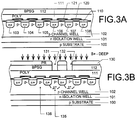
- Figs. 3A-3B illustrate a process for implanting the code implants according to preferred embodiments of the present invention.
- Fig. 3A illustrates a typical floating gate memory array in cross section prior to code implants.
- the array is formed on a p-type substrate 100.
- a n-type isolation well 101 is formed in the substrate 100.
- a p-type channel well 102 is formed in the isolation well.
- Buried diffusion bit lines 103-108 are formed in the channel well.
- Dielectric layer 110 is formed over the semiconductor substrate. The dielectric layer 110 is thinner over the channel regions of the cells between the bit line diffusions than over the diffusions themselves, forming a tunnel dielectric for the cells.
- a floating gate 120 is formed over the tunnel dielectric in each cell, which is covered by an interpoly dielectric 121.
- a polysilicon wordline 111 is formed over the interpoly dielectric 121 to create a row of floating gate cells.
- a passivation layer 112 such as borophosophosilicate glass
- the deep n-type isolation well 110 is formed in one embodiment as an early step in the integrated circuit manufacturing process, during which the n-type isolation well is patterned, and a phosphorous implant for example 6 x 10 12 /cm 2 is made at about 120 keV and yield at about 1050°C for about 12 hours.
- the p-type channel well 102 is implemented in this embodiment by patterning the p-type well, and executing a 7 x 10 12 /cm 2 boron implant at about 100 keV followed by an anneal at about 1050°C for about 3 hours and 10 minutes.
- n-type well in selected areas with a depth of about 6 microns, and a p-type well within selected areas of the n-type well with a depth of about 3 microns.
- the parameters of the process for forming the n-type and p-type wells will vary from embodiment to embodiment, to suit particular design needs.
- the floating gate cell manufacturing steps in Fig. 3A can be done in a variety of technologies as well. See for example U.S. Patent No. 5,526,707 entitled FLASH EPROM INTEGRATED CIRCUIT ARCHITECTURE invented by Tom D.H. Yiu, et al.
- a deep implant step as illustrated in Fig. 3B is executed.
- Fig. 3B illustrates the implementation of a photo resist mask 130 over the passivation layer 112.
- the photo resist mask is used to expose channel regions 131, 132 of selected cells in the array.
- a deep boron implant in this embodiment is implanted with an ion implantation process with an energy in a range of 175-500 keV, more preferably in a range of 200-250 keV.
- the ROM code implant step results in cells storing ROM mode data. For example, cell 135 stores the bit (0). Cell 136 stores the bit (1).
- Fig. 4 is a simplified diagram of an integrated circuit memory device according to preferred embodiments of the present invention.
- the integrated circuit memory includes an array of flash memory/ROM cells 300 such as that illustrated with respect to Figs. 1 and 3A-3B.
- the array of cells 300 is formed in a channel well 301.
- a row decoder 302 and a column decoder 303 are coupled with the array 300.
- An address is supplied on line 304 to the row decoder and column decoder to select a particular cell.
- the data of the accessed cell is supplied through the column decoder circuitry into a read state machine 305 through which the output data 306 is supplied.
- the read state machine 305 is coupled to well bias circuits 307 controlling the substrate bias in the channel well 301 as discussed above.
- the device also includes program, erase state machine 310, which is coupled to the array, the row decoder and the column decoder as known in the art.
- program, erase state machine 310 which is coupled to the array, the row decoder and the column decoder as known in the art.
- the floating gate memory array is implemented with a sector architecture allowing sector by sector erase operation, such as described in U.S. Patent No. 5,414,664, entitled FLASH EPROM WITH BLOCK ERASE FLAGS FOR OVER-ERASE PROTECTION.
- the state machine is programmed to execute a process which involves first receiving a read data command (step 400).
- the read data command is interpreted to determine whether a flash or ROM mode read is demanded (step 401). If a flash mode read is selected, the channel well is set to a first level, such as ground, (step 402) and the data is read (step 403).
- the program and erase algorithms operate to set the thresholds of the cells with and without the deep implants according to standard program/verify/retry algorithms. See for example U.S. Patent No 5,463,586, entitled ERASE AND PROGRAM VERIFICATION CIRCUIT FOR NON-VOLATILE MEMORY.
- the read state machine initiates a sector erase operation for the sector to be read, compensating for the charge on the floating gates by erasing the sector before the read process (step 404).
- the process involves setting the channel well to a ROM mode bias level, such as -2 volts (step 405).
- the wordline decoder is used to select a wordline and set it to a ROM mode read voltage and the data is read (step 406).
- the ROM mode read voltage corresponds to the voltage V WLR 60 of Fig. 2.
- the state machine is programmed to execute a process which involves first receiving a read data command (step 410).
- the read data command is interpreted to determine whether a flash or ROM mode read is demanded (step 411). If a flash mode read is selected, the channel well is set to a first level, such as ground, (step 412) and the data is read (step 413).
- the flash mode the data in the cell is determined predominantly by the charge in the floating gate of the cells.
- the deep implants do not significantly affect the thresholds.
- the program and erase algorithms operate to set the thresholds of the cells with and without the deep implants according to standard program/verify/retry algorithms, as mentioned above..
- the read state machine initiates a first read to determine the threshold of the cells being read under the normal substrate bias, in order to compensate for the charge on the floating gates (step 414).
- the process involves setting the channel well to a ROM mode bias level, such as -2 volts (step 415).
- the wordline decoder is used to select a wordline and set it to a ROM mode read voltage which has a first level for cells having a high threshold state due to charge in the floating gate, such as at a level above point 53 in Fig. 2, and a second level for cells having a low threshold state due to charge in the floating gate, such as at a level above point 51 in Fig. 2, and the data is read (step 416).
- the charge stored on the floating gate is compensated for by first sensing the threshold of the cell without substrate bias, and then with substrate bias, in order to determine whether a ROM code implant has been made in the cell, using for example a binary search method in the sensing circuitry to sense the data. This way, the sector subject of the ROM mode read operation need not be erased to compensate for charge in the floating gates of cells.
- FIG. 7 illustrates an embodiment in which there are a plurality of channel wells along with a corresponding plurality of separate arrays of floating gate memory cells.
- the semiconductor substrate is represented by the outer box 600.
- the isolation well is shaded box 601.
- the channel wells in the figure include channel well 602, channel well 603 and channel well 604.
- the arrays of floating gate memory cells in the device of Fig. 7 are illustrated in a simplified format, with the drain and source diffusion regions and word lines shown.
- drain-source-drain structure of Figs. 7 and 8 are presently preferred, other architectures are suitable, such as a virtual ground architecture with continuous arrays.
- drain-source-drain structures are shown in channel well 602, in which a drain diffusion 606, a source diffusion 607 and a drain diffusion 608 define two columns of cells, and in which word lines 610, 611, 612, 613 intersect the drain diffusion 606, source diffusion 607, and drain diffusion 608 over memory cells.
- additional drain-source-drain structures 615, 616 are included to provide an array within the channel well 602.
- the isolation well 601, the drama diffusion regions 606 and 608, and the source diffusion regions 607 all have the same conductivity type, preferably n-type.
- the substrate 600 and the channel region 602 are both of the same conductivity type, preferably p-type.
- the arrays in other channel wells 603 and 604 are configured with a similar structure.
- a plurality of word lines 620 is included for channel well 603. Drain-source-drain structures 621, 622, 623 within channel well 603 intersected by the word lines 620 form the array of flash memory cells.
- the channel well 604 includes an array of flash memory cells composed of the word lines 630, and the drain-source-drain structures 631, 632 and 633.
- This architecture is suitable for systems in which it is desirable to erase arrays having a block size equal to that of the channel well, such as the channel well 603.
- the channel wells can be individually biased to avoid disturbance of unselected cells, and to reduce stress on peripheral devices outside of the array on the substrate.
- Fig. 7 the deep implants established by the masking operation of Figs. 3A-3B, for ROM mode reading, are represented by the "X" symbols in the channels of the cells of channel well 603 for example.
- a first block includes a set of drain-source-drain structures 710, 711, 712 and a set of word lines 713.
- the individual flash memory cells reside between the source and drain diffusions and underneath the word lines in the array.
- a second block of cells is based on drain-source-drain structures 720, 721 and 722 with word lines 723.
- a third set of cells is based on drain-source-drain structures 730, 731 and 732, with word lines 733.
- Fig. 8 as in Fig. 7, the deep implants established by the masking operation of Figs. 3A-3B, for ROM mode reading, are represented by the "X" symbols in the channels of the cells in one sector for example.
Abstract
Description
- The present invention relates to integrated circuit memories, and more particularly to a dual mode memory cell, having for example a read only mode and another mode, an erasable and programmable mode.
- The cost of integrated circuit memory devices is closely related to the amount of area on an integrated circuit that is required to store a given amount of data, a parameter often referred to as the density of the device. By saving area on an integrated circuit, a manufacturer is able to make more chips with a given wafer in the fabrication factory. More chips per wafer translates directly to cost savings which can then be passed on to the consumers of the memory devices.
- One avenue for increasing the density of memory devices involves storing more than one bit per memory cell. Thus for example, the ability to store two bits per cell allows twice the data density on an integrated circuit.
- Multiple bit per cell technologies have been developed for floating gate memory devices. See U.S. Patent No. 5,163,021 to Mehrotra, et al. However, the floating gate memory approach involves complex charging and discharging of the floating gates, and difficult sensing technology, which increases the complexity and reduces the reliability of the devices.
- Another technique for increasing the density of memory devices involves multiple layers of memory cells in a given area on the device. This is typically implemented using thin film techniques in which transistors are stacked on top of one another, creating more than one memory cell per unit area. Typical prior art in this area includes U.S. Patent No. 5,358,887 invented by Hong. The multi-layer approach requires special manufacturing steps, and special decoding circuitry which increase cost and reduce reliability.
- Another characteristic of memory devices arises from the type of data to be stored in them. Some data, such as boot code and initialization parameters are read only rarely during operation of a circuit in which the data is stored. Other data is read often, but not changed. For other kinds of data, it is important to be able to dynamically change it, yet maintain it in a non-volatile form. These different kinds of data are often kept in different memory devices designed for the particular use pattern. Thus, for example, boot code which need not be changed in a system, is often stored in read only memory, because of the low cost. Other kinds of more fluid programs are often stored in flash memory. However, to accommodate the different kinds of storage, designers are required to include more than one memory chip on the system.
- Accordingly, there is a need for a simpler, low cost technique for implementing multiple bits per cell in a memory device, and providing for read only and programmable modes in a single device.
- Viewed from a first aspect, the present invention provides an integrated circuit memory, comprising:
- an array of memory cells storing data according to a first storage mode, the memory cells comprising transistors having channels in channel regions of a semiconductor substrate, and having threshold voltages dependent on a dope concentration in the channel regions, the array including a first set of memory cells with a base dope concentration in the channel regions, and a second set of memory cells in the array with code implants which change dope concentrations in the channel regions;
- a plurality of word lines and bit lines coupled respectively with rows and columns of memory cells in the array by which to read data stored in the array; and
- resources to apply a first bias potential to channel regions of transistors in the memory cells in the array during a first read mode at which the memory cells have particular threshold voltages and to sense data stored according to the first storage mode, and to apply a second bias potential to channel regions of memory cells in the array during a second read mode to induce a shift in the threshold voltages in the memory cells, the shift being different in the second set of memory cells than in the first set of memory cells, due to the code implants, and to sense data stored by the code implants.
-
- Viewed from a second aspect, the present invention provides an integrated circuit memory, comprising:
- an array of floating gate memory cells, the memory cells comprising floating gate transistors having channels in channel regions of a semiconductor substrate, and having threshold voltages dependent on a dope concentration in the channel regions and on charge in the floating gates, the array including a first set of memory cells with a base dope concentration in the channel regions, and a second set of memory cells in the array with code implants which change dope concentrations in the channel regions;
- a plurality of word lines and bit lines coupled respectively with rows and columns of memory cells in the array by which to read data stored in the array, and by which to charge and discharge the floating gates of memory cells in the array; and
- resources to apply a first bias potential to channel regions of memory cells in the array at which the memory cells have particular threshold voltages, and to apply a second bias potential to channel regions of memory cells to induce a shift in the threshold voltages in the memory cells, the shift being different in the second set of memory cells than in the first set of memory cells, due to the code implants.
-
- In accordance with preferred embodiments of the present invention, a dual mode memory cell and integrated circuit including a ROM mode and a native mode is provided. According to preferred embodiments of the present invention, ROM code implants are incorporated into a memory array designed for a native mode of operation. The implants are deep implants which do not have a large effect on the threshold of the cell under normal substrate bias conditions. However, as the substrate bias is increased, they have an increasing effect on the cell threshold. Thus, the cells in one embodiment of the invention comprise floating gate memory cells that can be read in a flash mode, in which the threshold of the cell is determined predominantly by charge stored in the floating gate of the cell, and in a read only mode during which a substrate bias is applied, the charge stored in the floating gates in the sector to be read are equalized or otherwise compensated for, and the threshold of the cell is determined predominately by the ROM code implants. Thus, more than one bit per cell is stored in the device, where one bit is stored in a read only mode and another bit is stored in a programmable and erasable mode in each cell in at least one sector of the memory device. Other memory device native modes to which embodiments of the present invention are applied include static random access memory SRAM, dynamic random access memory DRAM, ferro-electric random access memory FRAM, EPROM, and others.
- A preferred embodiment of the present invention can be characterized as an integrated circuit memory that comprises an array of floating gate memory cells. The memory cells comprise floating gate transistors having channel regions in a semiconductor substrate and having threshold voltages dependent on a dope concentration in the channel regions and on charge in the floating gates. The array includes a first set of memory cells with a base dope concentration in the channel regions, and a second set of memory cells in the array with code implants which change the dope concentrations in the channel regions. A plurality of wordlines and bitlines are coupled respectively with rows and columns of memory cells in the array by which to read data stored in the array, and by which to charge and discharge the floating gates of memory cells in the array. Resources on the chip are provided to apply a first bias potential to the channel regions of memory cells in the array at which the memory cells have a particular threshold voltages, and to apply a second bias potential to channel regions of memory cells to induce a shift in the threshold voltages in the memory cells by the body effect. The shift due to the body effect is greater in the second set of memory cells than in the first set of memory cells due to the code implants.
- The integrated circuit memory preferably also includes resources to read memory cells in the array in a first mode during which the first bias potential is applied to the channel regions, and the threshold voltages of the memory cells are determined predominately by charge in the floating gates. Also, the resources include circuitry to read the cells in a second mode during which the second bias potential is applied to the channel regions and charge in the floating gates to be read in the array is equalized. In the second mode, the threshold voltages of the memory cells are determined predominately by the presence or absence of code implants.
- The code implants in a preferred embodiment comprise boron and have a depth in the channel regions of the second set of memory cells according to an implantation with an ion implantation process at an energy which is high enough to create deep implants allowing for the threshold conditions outlined above. Thus for example the ion implantation process of boron in a silicon substrate has an energy in the range of 175 to 500 keV, and more preferably in the range of 200 to 250 keV.
- According to another aspect of preferred embodiments of the invention, the array of floating gate memory cells includes a plurality of sectors. The resources are operable to read in the ROM mode on a sector by sector basis. According to another aspect, the ROM code implants are implanted in only one sector of the plurality of sectors in the device.
- Accordingly, a flexible integrated circuit memory device may be provided having a read only memory mode and a native mode, such as an erasable and programmable mode, for a single cell or a single array on the device. This enables storing persistent data in the ROM mode on the device, while providing the ability to use the same memory cells for erasable and programmable operation. This multiple bit per cell approach based on two read modes vastly saves in board space and increases memory density in a unique way.
- Other aspects and advantages of the present invention can be seen upon review of the figures, the detailed description, and the claims which follow.
-
- Fig. 1 illustrates the dual mode, floating gate memory, mask ROM cell according to preferred embodiments of the present invention in two coding states for the ROM mode, according to preferred embodiments of the present invention.
- Fig. 2 is a graph illustrating the threshold voltage shift induced by increasing substrate bias.
- Fig. 3A - 3B illustrate the code implant process according to preferred embodiments of the present invention for the dual mode device of preferred embodiments of the present invention.
- Fig. 4 is a simplified block diagram of an integrated circuit memory including an array of dual mode memory cells according to preferred embodiments of the present invention.
- Fig. 5 is a flow chart illustrating a read process for the integrated circuit memory of Fig. 4.
- Fig. 6 is a flow chart illustrating another read process for the integrated circuit memory of Fig. 4.
- Fig. 7 illustrates a triple well architecture for a dual mode array, with sector by sector channel wells.
- Fig. 8 illustrates a triple well architecture for a dual mode array, with a single channel well.
-
- A detailed description of preferred embodiments of the present invention is provided with respect to Figs. 1-8. A cell structure for implementing the dual mode cell is described with reference to Figs. 1 and 2. A manufacturing process, architecture for integrated circuits, and a reading technique are described with respect to Figs. 3-8.
- Fig. 1 shows two floating gate/ROM cells having the two ROM code implant states according to preferred embodiments of the present invention. Thus,
cell 1 is a n-channel floating gate transistor formed in asemiconductor substrate 10. The n-channel transistor includes acontrol gate 11, such as formed by a wordline in a memory array, a floatinggate 11A, adrain 12 formed by a n-type implant in thesubstrate 10, and asource 13 formed by a n-type implant in thesubstrate 10. The n-channel cell according to the present invention is formed in achannel well 14. The channel well 14 itself is implemented inside anisolation well 15. The isolation well 15 is formed in a p-type semiconductor substrate 16. The channel well 14 is coupled to asubstrate bias terminal 17 by which a substrate bias potential is applied to the channel regions of the n-channel transistor. In a preferred embodiment, the channel region is formed with a p- implant referred to as a VT adjustment implant used to raise the threshold voltage of the n-channel transistor relative to that of a cell not having the implant. This base implant may or may not be necessary depending on the concentration of thechannel well 14. Thus,cell 1 in Fig. 1 corresponds to a dual mode cell having only the VT adjustimplant 18, and no code implant. -
Cell 2 in Fig. 1 illustrates a deep code implant according to preferred embodiments of the present invention. The elements ofcell 2 which correspond to the same elements incell 1 have like reference numbers. Thus,cell 2 includes the VT adjust implant, represented by theregion 18, and a deep implant represented by theregion 20. Thedeep implant 20 will have a concentration of dopants greater than the VT adjust implant inregion 18, and be implanted with a higher energy such that its depth is greater than the VT adjust implant. - In cells 1-2, the threshold voltage VT, that is the voltage between the
control gate 11 and thesource 13 at which current is conducted in the transistor, is determined predominantly by a combination of the charge in the floatinggate 11A, the dope concentrations in the channel of the cell, and by the substrate bias potential 17 applied to thechannel well 14. - Fig. 2 is a simplified graph showing the relationship of threshold voltage VT to substrate bias voltage VSB, assuming equal charges on the floating gates. For
cell 1, a threshold voltage VT01 atpoint 50 is determined predominately by the VT adjust implant. As the substrate bias potential VSB increases, the threshold ofcell 1 increases as well. At a critical substrate bias potential VSBC, the threshold ofcell 1 is seen atpoint 51. - For
cell 2, the threshold voltage VT02 is found atpoint 52, and at the substrate bias VSBC, threshold voltage is found atpoint 53. As can be seen, the shift in threshold voltage induced by the increasing substrate bias potential is greater incell 2 than it is incell 1 due to thedeep implant 20. - Accordingly, as can be seen in Fig. 2 a reading circuit in a ROM mode, can discriminate between
cells point 61, so long as the floating gate charge is first equalized such as by an erase operation (or a program operation) on the cells to be read in the ROM mode. - The substrate potential VSB in Fig. 2 is negative for a n-channel device such as cells 1-2 in Fig. 1. For a p-channel device, the substrate potential is positive.
- Figs. 3A-3B illustrate a process for implanting the code implants according to preferred embodiments of the present invention. Fig. 3A illustrates a typical floating gate memory array in cross section prior to code implants. Thus the array is formed on a p-
type substrate 100. A n-type isolation well 101 is formed in thesubstrate 100. A p-type channel well 102 is formed in the isolation well. Buried diffusion bit lines 103-108 are formed in the channel well.Dielectric layer 110 is formed over the semiconductor substrate. Thedielectric layer 110 is thinner over the channel regions of the cells between the bit line diffusions than over the diffusions themselves, forming a tunnel dielectric for the cells. A floatinggate 120, is formed over the tunnel dielectric in each cell, which is covered by aninterpoly dielectric 121. Apolysilicon wordline 111 is formed over theinterpoly dielectric 121 to create a row of floating gate cells. Apassivation layer 112 such as borophosophosilicate glass BPSG is formed over the wordline. - The deep n-
type isolation well 110 is formed in one embodiment as an early step in the integrated circuit manufacturing process, during which the n-type isolation well is patterned, and a phosphorous implant for example 6 x 10¹²/cm2 is made at about 120 keV and yield at about 1050°C for about 12 hours. The p-type channel well 102 is implemented in this embodiment by patterning the p-type well, and executing a 7 x 10¹²/cm2 boron implant at about 100 keV followed by an anneal at about 1050°C for about 3 hours and 10 minutes. This processing results in a n-type well in selected areas with a depth of about 6 microns, and a p-type well within selected areas of the n-type well with a depth of about 3 microns. The parameters of the process for forming the n-type and p-type wells will vary from embodiment to embodiment, to suit particular design needs. The floating gate cell manufacturing steps in Fig. 3A can be done in a variety of technologies as well. See for example U.S. Patent No. 5,526,707 entitled FLASH EPROM INTEGRATED CIRCUIT ARCHITECTURE invented by Tom D.H. Yiu, et al. - To implement the code implants according to preferred embodiments of the present invention a deep implant step as illustrated in Fig. 3B is executed.
- Fig. 3B illustrates the implementation of a photo resist
mask 130 over thepassivation layer 112. The photo resist mask is used to exposechannel regions cell 135 stores the bit (0).Cell 136 stores the bit (1). - Fig. 4 is a simplified diagram of an integrated circuit memory device according to preferred embodiments of the present invention. The integrated circuit memory includes an array of flash memory/
ROM cells 300 such as that illustrated with respect to Figs. 1 and 3A-3B. The array ofcells 300 is formed in achannel well 301. Arow decoder 302 and acolumn decoder 303 are coupled with thearray 300. An address is supplied online 304 to the row decoder and column decoder to select a particular cell. The data of the accessed cell is supplied through the column decoder circuitry into aread state machine 305 through which theoutput data 306 is supplied. The readstate machine 305 is coupled towell bias circuits 307 controlling the substrate bias in the channel well 301 as discussed above. The device also includes program, erasestate machine 310, which is coupled to the array, the row decoder and the column decoder as known in the art. In a preferred embodiment, the floating gate memory array is implemented with a sector architecture allowing sector by sector erase operation, such as described in U.S. Patent No. 5,414,664, entitled FLASH EPROM WITH BLOCK ERASE FLAGS FOR OVER-ERASE PROTECTION. - The operation of the read
state machine 305 can be understood with reference to Fig. 5 according to one example. According to the technique shown in Fig. 5, the state machine is programmed to execute a process which involves first receiving a read data command (step 400). The read data command is interpreted to determine whether a flash or ROM mode read is demanded (step 401). If a flash mode read is selected, the channel well is set to a first level, such as ground, (step 402) and the data is read (step 403). In the flash mode, the data in the cell is determined predominantly by the charge in the floating gate of the cells. The deep implants do not significantly affect the thresholds. Further, the program and erase algorithms operate to set the thresholds of the cells with and without the deep implants according to standard program/verify/retry algorithms. See for example U.S. Patent No 5,463,586, entitled ERASE AND PROGRAM VERIFICATION CIRCUIT FOR NON-VOLATILE MEMORY. - If at
step 401, the ROM mode is selected, the read state machine initiates a sector erase operation for the sector to be read, compensating for the charge on the floating gates by erasing the sector before the read process (step 404). Next, the process involves setting the channel well to a ROM mode bias level, such as -2 volts (step 405). The wordline decoder is used to select a wordline and set it to a ROM mode read voltage and the data is read (step 406). The ROM mode read voltage corresponds to the voltage VWLR 60 of Fig. 2. - The operation of the read
state machine 305 can be understood with reference to Fig. 6 according to another example. According to the technique shown in Fig. 6, the state machine is programmed to execute a process which involves first receiving a read data command (step 410). The read data command is interpreted to determine whether a flash or ROM mode read is demanded (step 411). If a flash mode read is selected, the channel well is set to a first level, such as ground, (step 412) and the data is read (step 413). In the flash mode, the data in the cell is determined predominantly by the charge in the floating gate of the cells. The deep implants do not significantly affect the thresholds. Further, the program and erase algorithms operate to set the thresholds of the cells with and without the deep implants according to standard program/verify/retry algorithms, as mentioned above.. - If at step 411, the ROM mode is selected, the read state machine initiates a first read to determine the threshold of the cells being read under the normal substrate bias, in order to compensate for the charge on the floating gates (step 414). Next, the process involves setting the channel well to a ROM mode bias level, such as -2 volts (step 415). The wordline decoder is used to select a wordline and set it to a ROM mode read voltage which has a first level for cells having a high threshold state due to charge in the floating gate, such as at a level above
point 53 in Fig. 2, and a second level for cells having a low threshold state due to charge in the floating gate, such as at a level abovepoint 51 in Fig. 2, and the data is read (step 416). - In the alterative approach of Fig. 6, the charge stored on the floating gate is compensated for by first sensing the threshold of the cell without substrate bias, and then with substrate bias, in order to determine whether a ROM code implant has been made in the cell, using for example a binary search method in the sensing circuitry to sense the data. This way, the sector subject of the ROM mode read operation need not be erased to compensate for charge in the floating gates of cells.
- Two basic architectures are shown in Fig. 7 and Fig. 8 for laying out the isolation well and channel well according to preferred embodiments of the present invention. Fig. 7 illustrates an embodiment in which there are a plurality of channel wells along with a corresponding plurality of separate arrays of floating gate memory cells. In Fig. 7, the semiconductor substrate is represented by the
outer box 600. The isolation well is shadedbox 601. The channel wells in the figure include channel well 602, channel well 603 and channel well 604. As represented in the figure, there may be a number of channel wells with corresponding arrays of floating gate memory cells in each one. The arrays of floating gate memory cells in the device of Fig. 7 are illustrated in a simplified format, with the drain and source diffusion regions and word lines shown. The global bit lines, block select circuitry, and other circuits necessary for completing the structure and not illustrated in the figure, are well understood by persons of skill in the art. For instance, this architecture can be implemented as described in U.S. Patent No. 5,399,891, U.S. Patent No. 5,414,664, or U.S. Patent No. 5,526,307. - Although the drain-source-drain structure of Figs. 7 and 8 are presently preferred, other architectures are suitable, such as a virtual ground architecture with continuous arrays.
- In this example, a plurality of drain-source-drain structures are shown in channel well 602, in which a
drain diffusion 606, asource diffusion 607 and adrain diffusion 608 define two columns of cells, and in which word lines 610, 611, 612, 613 intersect thedrain diffusion 606,source diffusion 607, anddrain diffusion 608 over memory cells. Within the channel well 602, additional drain-source-drain structures channel well 602. As illustrated in the figure by the shading, the isolation well 601, thedrama diffusion regions source diffusion regions 607, all have the same conductivity type, preferably n-type. Thesubstrate 600 and thechannel region 602 are both of the same conductivity type, preferably p-type. - The arrays in
other channel wells word lines 620 is included for channel well 603. Drain-source-drain structures - In a similar fashion the channel well 604 includes an array of flash memory cells composed of the word lines 630, and the drain-source-
drain structures - This architecture is suitable for systems in which it is desirable to erase arrays having a block size equal to that of the channel well, such as the
channel well 603. The channel wells can be individually biased to avoid disturbance of unselected cells, and to reduce stress on peripheral devices outside of the array on the substrate. - In Fig. 7, the deep implants established by the masking operation of Figs. 3A-3B, for ROM mode reading, are represented by the "X" symbols in the channels of the cells of channel well 603 for example.
- For a smaller array size, and a smaller overall integrated circuit size, the architecture of Fig. 8 is suitable. According to the architecture Fig. 8,
substrate 700 has a first conductivity type, such as p-type. An isolation well 701 has a second conductivity type, preferably n-type. A channel well 702 is formed within the isolation well 701, having a conductivity type which is the same as that of the substrate. A plurality of blocks of floating gate memory cells is formed within the channel well 702 to produce a large array. Thus, a first block includes a set of drain-source-drain structures drain structures drain structures - In Fig. 8, as in Fig. 7, the deep implants established by the masking operation of Figs. 3A-3B, for ROM mode reading, are represented by the "X" symbols in the channels of the cells in one sector for example.
- Accordingly, a low cost and simple to manufacture dual mode flash memory/ROM device has been provided taking advantage of the non-linearity of the body effect with doping concentration, particularly in the presence of deep implants.
- The foregoing description of a preferred embodiment of the invention has been presented for purposes of illustration and description. It is not intended to be exhaustive or to limit the invention to the precise forms disclosed. Obviously, many modifications and variations will be apparent to practitioners skilled in this art.
Claims (15)
- An integrated circuit memory, comprising:an array of memory cells storing data according to a first storage mode, the memory cells comprising transistors having channels in channel regions of a semiconductor substrate, and having threshold voltages dependent on a dope concentration in the channel regions, the array including a first set of memory cells with a base dope concentration in the channel regions, and a second set of memory cells in the array with code implants which change dope concentrations in the channel regions;a plurality of word lines and bit lines coupled respectively with rows and columns of memory cells in the array by which to read data stored in the array; andresources to apply a first bias potential to channel regions of transistors in the memory cells in the array during a first read mode at which the memory cells have particular threshold voltages and to sense data stored according to the first storage mode, and to apply a second bias potential to channel regions of memory cells in the array during a second read mode to induce a shift in the threshold voltages in the memory cells, the shift being different in the second set of memory cells than in the first set of memory cells, due to the code implants, and to sense data stored by the code implants.
- The integrated circuit memory of claim 1, wherein the transistors in the memory cells comprise floating gate transistors, and the threshold voltages of the memory cells are determined predominantly by charge in the floating gates during the first read mode, and in a second mode during which the second bias potential is applied to the channel regions, in which charge in floating gates of cells to be read in the array is compensated for, and the threshold voltages of the memory cells are determined predominantly by presence or absence of the code implants.
- An integrated circuit memory, comprising:an array of floating gate memory cells, the memory cells comprising floating gate transistors having channels in channel regions of a semiconductor substrate, and having threshold voltages dependent on a dope concentration in the channel regions and on charge in the floating gates, the array including a first set of memory cells with a base dope concentration in the channel regions, and a second set of memory cells in the array with code implants which change dope concentrations in the channel regions;a plurality of word lines and bit lines coupled respectively with rows and columns of memory cells in the array by which to read data stored in the array, and by which to charge and discharge the floating gates of memory cells in the array; andresources to apply a first bias potential to channel regions of memory cells in the array at which the memory cells have particular threshold voltages, and to apply a second bias potential to channel regions of memory cells to induce a shift in the threshold voltages in the memory cells, the shift being different in the second set of memory cells than in the first set of memory cells, due to the code implants.
- The integrated circuit memory of claim 3, including:resources to read memory cells in the array in a first mode during which the first bias potential is applied to the channel regions, and the threshold voltages of the memory cells are determined predominantly by charge in the floating gates, and in a second mode during which the second bias potential is applied to the channel regions, in which charge in floating gates of cells to be read in the array is compensated for, and the threshold voltages of the memory cells are determined predominantly by presence or absence of the code implants.
- The integrated circuit memory of any preceding claim, wherein the memory cells comprise n-channel floating gate transistors, and wherein the second bias potential is negative, and the first bias potential is ground.
- The integrated circuit memory of any preceding claim, wherein the second bias potential has an absolute value greater than the first bias potential.
- The integrated circuit memory of any preceding claim when dependent on claim 1, wherein the transistors in the array of memory cells include base implants to establish the base dope concentration.
- The integrated circuit memory of any preceding claim when dependent on claim 3, wherein the array of floating gate memory cells includes a base implant to establish the base dope concentration.
- The integrated circuit memory of any preceding claim, wherein the array of memory cells includes a base implant to establish the base dope concentration.
- The integrated circuit memory of any preceding claim, wherein the code implants comprise p-type dopants.
- The integrated circuit memory of any preceding claim, wherein the code implants comprise boron and have a depth in the channel regions of the second set of memory cells according to implantation with an ion implantation process at an energy in a range of 175 to 500 keV.
- The integrated circuit memory of any preceding claim, wherein the code implants comprise boron and have a depth in the channel regions of the second set of memory cells according to implantation with an ion implantation process at an energy in a range of 200 to 250 keV.
- The integrated circuit memory of any preceding claim when dependent on claim 1, wherein the array of memory cells includes a plurality of sectors, and the resources to apply the second bias potential are coupled to the plurality of sectors, and enabled on a sector by sector basis.
- The integrated circuit memory of any preceding claim when dependent on claim 3, wherein the array of floating gate memory cells includes a plurality of sectors, and the resources to apply the second bias potential are coupled to the plurality of sectors, and enabled on a sector by sector basis.
- The integrated circuit memory of claim 13 or claim 14, wherein the second set of memory cells consist of cells in a single sector in the plurality of sectors.
Applications Claiming Priority (2)
| Application Number | Priority Date | Filing Date | Title |
|---|---|---|---|
| US926342 | 1997-09-09 | ||
| US08/926,342 US5822243A (en) | 1997-09-09 | 1997-09-09 | Dual mode memory with embedded ROM |
Publications (2)
| Publication Number | Publication Date |
|---|---|
| EP0902477A1 true EP0902477A1 (en) | 1999-03-17 |
| EP0902477B1 EP0902477B1 (en) | 2002-05-29 |
Family
ID=25453082
Family Applications (1)
| Application Number | Title | Priority Date | Filing Date |
|---|---|---|---|
| EP97307414A Expired - Lifetime EP0902477B1 (en) | 1997-09-09 | 1997-09-23 | Dual mode memory with embedded rom |
Country Status (3)
| Country | Link |
|---|---|
| US (1) | US5822243A (en) |
| EP (1) | EP0902477B1 (en) |
| DE (1) | DE69712883T2 (en) |
Cited By (1)
| Publication number | Priority date | Publication date | Assignee | Title |
|---|---|---|---|---|
| FR2857497A1 (en) * | 2003-07-11 | 2005-01-14 | Samsung Electronics Co Ltd | MEMORY DEVICE WITH INTEGRATED CIRCUIT |
Families Citing this family (17)
| Publication number | Priority date | Publication date | Assignee | Title |
|---|---|---|---|---|
| US6009017A (en) * | 1998-03-13 | 1999-12-28 | Macronix International Co., Ltd. | Floating gate memory with substrate band-to-band tunneling induced hot electron injection |
| EP0991118B1 (en) | 1998-10-02 | 2006-01-18 | STMicroelectronics S.r.l. | Method for realizing a multilevel ROM memory in a dual gate CMOS process and corresponding ROM memory cell |
| EP1024527A3 (en) * | 1998-12-31 | 2001-05-23 | STMicroelectronics S.r.l. | Method for obtaining a multi-value ROM in an EEPROM process flow |
| US6576517B1 (en) | 1998-12-31 | 2003-06-10 | Stmicroelectronics S.R.L. | Method for obtaining a multi-level ROM in an EEPROM process flow |
| US6060742A (en) * | 1999-06-16 | 2000-05-09 | Worldwide Semiconductor Manufacturing Corporation | ETOX cell having bipolar electron injection for substrate-hot-electron program |
| US6801453B2 (en) * | 2002-04-02 | 2004-10-05 | Macronix International Co., Ltd. | Method and apparatus of a read scheme for non-volatile memory |
| US6961807B1 (en) | 2002-08-27 | 2005-11-01 | Cypress Semiconductor Corporation | Device, system and method for an integrated circuit adaptable for use in computing systems of differing memory requirements |
| KR100506934B1 (en) * | 2003-01-10 | 2005-08-05 | 삼성전자주식회사 | Polishing apparatus and the polishing method using the same |
| JP3941943B2 (en) * | 2003-03-12 | 2007-07-11 | 力旺電子股▲ふん▼有限公司 | ROM |
| US7119393B1 (en) * | 2003-07-28 | 2006-10-10 | Actel Corporation | Transistor having fully-depleted junctions to reduce capacitance and increase radiation immunity in an integrated circuit |
| CN100463138C (en) * | 2004-04-26 | 2009-02-18 | 旺宏电子股份有限公司 | Operation scheme with charge balancing erase for charge trapping non-volatile memory |
| KR100604877B1 (en) * | 2004-07-03 | 2006-07-31 | 삼성전자주식회사 | Apparatus and method for controlling memory address mapping in embedded system |
| CN102938409B (en) * | 2012-11-07 | 2015-09-23 | 南京大学 | Based on pair transistor light-sensitive detector and the signal-obtaining way thereof of compound medium grid MOSFET |
| US9620953B2 (en) | 2013-03-25 | 2017-04-11 | Wen Technology, Inc. | Methods providing control for electro-permanent magnetic devices and related electro-permanent magnetic devices and controllers |
| JP2015176612A (en) * | 2014-03-13 | 2015-10-05 | 株式会社東芝 | Nonvolatile semiconductor memory device |
| US9620216B2 (en) | 2015-02-17 | 2017-04-11 | Silicon Storage Technology, Inc. | Flash memory device configurable to provide read only memory functionality |
| US10734149B2 (en) | 2016-03-23 | 2020-08-04 | Wen Technology Inc. | Electro-permanent magnetic devices including unbalanced switching and permanent magnets and related methods and controllers |
Citations (4)
| Publication number | Priority date | Publication date | Assignee | Title |
|---|---|---|---|---|
| JPS60211699A (en) * | 1984-04-06 | 1985-10-24 | Hitachi Ltd | Semiconductor integrated circuit device |
| US4667217A (en) * | 1985-04-19 | 1987-05-19 | Ncr Corporation | Two bit vertically/horizontally integrated memory cell |
| JPH02133967A (en) * | 1988-11-14 | 1990-05-23 | Sharp Corp | Semiconductor device |
| US5403764A (en) * | 1992-04-28 | 1995-04-04 | Rohm Co., Ltd. | Method for producing a ROM on a semiconductor device having a nonvolatile memory |
Family Cites Families (13)
| Publication number | Priority date | Publication date | Assignee | Title |
|---|---|---|---|---|
| US4864374A (en) * | 1987-11-30 | 1989-09-05 | Texas Instruments Incorporated | Two-transistor dram cell with high alpha particle immunity |
| US5163021A (en) * | 1989-04-13 | 1992-11-10 | Sundisk Corporation | Multi-state EEprom read and write circuits and techniques |
| JPH04115565A (en) * | 1990-09-05 | 1992-04-16 | Mitsubishi Electric Corp | Semiconductor memory device |
| JP3150747B2 (en) * | 1992-02-24 | 2001-03-26 | 株式会社リコー | Semiconductor memory device and method of manufacturing the same |
| JPH05283654A (en) * | 1992-04-03 | 1993-10-29 | Toshiba Corp | Mask rom and manufacture thereof |
| US5379253A (en) * | 1992-06-01 | 1995-01-03 | National Semiconductor Corporation | High density EEPROM cell array with novel programming scheme and method of manufacture |
| DE4422791C2 (en) * | 1993-06-29 | 2001-11-29 | Toshiba Kawasaki Kk | Semiconductor devices having a conductive film inducing an inversion layer in a surface area of a semiconductor substrate |
| US5358887A (en) * | 1993-11-26 | 1994-10-25 | United Microelectronics Corporation | Ulsi mask ROM structure and method of manufacture |
| US5574685A (en) * | 1994-09-01 | 1996-11-12 | Advanced Micro Devices, Inc. | Self-aligned buried channel/junction stacked gate flash memory cell |
| US5585297A (en) * | 1995-05-25 | 1996-12-17 | United Microelectronics Corporation | Method of manufacture of multi-state mask ROM and multi-state mask ROM device produced thereby |
| US5576573A (en) * | 1995-05-31 | 1996-11-19 | United Microelectronics Corporation | Stacked CVD oxide architecture multi-state memory cell for mask read-only memories |
| US5504030A (en) * | 1995-07-21 | 1996-04-02 | United Microelectronics Corporation | Process for fabricating high-density mask ROM devices |
| US5545580A (en) * | 1995-09-19 | 1996-08-13 | United Microelectronics Corporation | Multi-state read-only memory using multiple polysilicon selective depositions |
-
1997
- 1997-09-09 US US08/926,342 patent/US5822243A/en not_active Expired - Lifetime
- 1997-09-23 EP EP97307414A patent/EP0902477B1/en not_active Expired - Lifetime
- 1997-09-23 DE DE69712883T patent/DE69712883T2/en not_active Expired - Lifetime
Patent Citations (4)
| Publication number | Priority date | Publication date | Assignee | Title |
|---|---|---|---|---|
| JPS60211699A (en) * | 1984-04-06 | 1985-10-24 | Hitachi Ltd | Semiconductor integrated circuit device |
| US4667217A (en) * | 1985-04-19 | 1987-05-19 | Ncr Corporation | Two bit vertically/horizontally integrated memory cell |
| JPH02133967A (en) * | 1988-11-14 | 1990-05-23 | Sharp Corp | Semiconductor device |
| US5403764A (en) * | 1992-04-28 | 1995-04-04 | Rohm Co., Ltd. | Method for producing a ROM on a semiconductor device having a nonvolatile memory |
Non-Patent Citations (2)
| Title |
|---|
| PATENT ABSTRACTS OF JAPAN vol. 010, no. 074 (P - 439) 25 March 1986 (1986-03-25) * |
| PATENT ABSTRACTS OF JAPAN vol. 014, no. 371 (E - 0963) 10 August 1990 (1990-08-10) * |
Cited By (3)
| Publication number | Priority date | Publication date | Assignee | Title |
|---|---|---|---|---|
| FR2857497A1 (en) * | 2003-07-11 | 2005-01-14 | Samsung Electronics Co Ltd | MEMORY DEVICE WITH INTEGRATED CIRCUIT |
| US7102926B2 (en) | 2003-07-11 | 2006-09-05 | Samsung Electronics Co., Ltd. | Integrated circuit memory devices including programmed memory cells and programmable and erasable memory cells |
| US7379332B2 (en) | 2003-07-11 | 2008-05-27 | Samsung Electronics Co., Ltd. | Systems-on-chips including programmed memory cells and programmable and erasable memory cells |
Also Published As
| Publication number | Publication date |
|---|---|
| DE69712883T2 (en) | 2003-01-02 |
| EP0902477B1 (en) | 2002-05-29 |
| US5822243A (en) | 1998-10-13 |
| DE69712883D1 (en) | 2002-07-04 |
Similar Documents
| Publication | Publication Date | Title |
|---|---|---|
| US5822243A (en) | Dual mode memory with embedded ROM | |
| US6191975B1 (en) | Non-volatile NAND type semiconductor memory device with stacked gate memory cells and a stacked gate select transistor | |
| US7790562B2 (en) | Method for angular doping of source and drain regions for odd and even NAND blocks | |
| JP3906177B2 (en) | Nonvolatile semiconductor memory device | |
| US6504191B2 (en) | Independently programmable memory segments within a PMOS electrically erasable programmable read only memory array achieved by N-well separation and method therefor | |
| US5978264A (en) | Nonvolatile semiconductor memory device operable at high speed with low power supply voltage while suppressing increase of chip area | |
| JPH1145986A (en) | Non-volatile semiconductor storage device | |
| KR100379553B1 (en) | A array of flash memory cell and method for programming of data thereby and method for erased of data thereby | |
| US6396737B2 (en) | High density flash memory architecture with columnar substrate coding | |
| EP0642172B1 (en) | Semiconductor device having a non-volatile memory and method of manufacturing such a semiconductor device | |
| KR0135247B1 (en) | Flash memory cell and manufacture thereof | |
| US6215701B1 (en) | Nonvolatile memory cell structure for integration with semiconductor logic devices and method of using same | |
| JP4074694B2 (en) | Integrated circuit memory | |
| KR100792737B1 (en) | High density flash memory architecture with columnar substrate coding | |
| EP0902478B1 (en) | Multi-level memory array with channel bias algorithm | |
| US10916558B2 (en) | NOR flash memory and method of fabricating the same | |
| US6853027B2 (en) | Semiconductor nonvolatile memory with low programming voltage | |
| US6525959B1 (en) | NOR array with buried trench source line | |
| US5280187A (en) | Electrically programmable and erasable semiconductor memory and method of operating same | |
| JP3577290B2 (en) | Nonvolatile semiconductor memory device | |
| JP3198097B2 (en) | Nonvolatile semiconductor memory device | |
| JP2001358238A (en) | Nonvolatile semiconductor memory | |
| JP2001015615A (en) | Nonvolatile semiconductor storage device |
Legal Events
| Date | Code | Title | Description |
|---|---|---|---|
| PUAI | Public reference made under article 153(3) epc to a published international application that has entered the european phase |
Free format text: ORIGINAL CODE: 0009012 |
|
| AK | Designated contracting states |
Kind code of ref document: A1 Designated state(s): DE FR GB IT |
|
| AX | Request for extension of the european patent |
Free format text: AL;LT;LV;RO;SI |
|
| 17P | Request for examination filed |
Effective date: 19990816 |
|
| AKX | Designation fees paid |
Free format text: DE FR GB IT |
|
| 17Q | First examination report despatched |
Effective date: 20000912 |
|
| RAP1 | Party data changed (applicant data changed or rights of an application transferred) |
Owner name: MACRONIX INTERNATIONAL CO., LTD. |
|
| GRAG | Despatch of communication of intention to grant |
Free format text: ORIGINAL CODE: EPIDOS AGRA |
|
| GRAG | Despatch of communication of intention to grant |
Free format text: ORIGINAL CODE: EPIDOS AGRA |
|
| GRAH | Despatch of communication of intention to grant a patent |
Free format text: ORIGINAL CODE: EPIDOS IGRA |
|
| GRAH | Despatch of communication of intention to grant a patent |
Free format text: ORIGINAL CODE: EPIDOS IGRA |
|
| GRAA | (expected) grant |
Free format text: ORIGINAL CODE: 0009210 |
|
| AK | Designated contracting states |
Kind code of ref document: B1 Designated state(s): DE FR GB IT |
|
| REG | Reference to a national code |
Ref country code: GB Ref legal event code: FG4D |
|
| REF | Corresponds to: |
Ref document number: 69712883 Country of ref document: DE Date of ref document: 20020704 |
|
| ET | Fr: translation filed | ||
| PLBE | No opposition filed within time limit |
Free format text: ORIGINAL CODE: 0009261 |
|
| STAA | Information on the status of an ep patent application or granted ep patent |
Free format text: STATUS: NO OPPOSITION FILED WITHIN TIME LIMIT |
|
| 26N | No opposition filed |
Effective date: 20030303 |
|
| REG | Reference to a national code |
Ref country code: FR Ref legal event code: PLFP Year of fee payment: 20 |
|
| PGFP | Annual fee paid to national office [announced via postgrant information from national office to epo] |
Ref country code: FR Payment date: 20160705 Year of fee payment: 20 |
|
| PGFP | Annual fee paid to national office [announced via postgrant information from national office to epo] |
Ref country code: DE Payment date: 20160705 Year of fee payment: 20 Ref country code: GB Payment date: 20160704 Year of fee payment: 20 |
|
| PGFP | Annual fee paid to national office [announced via postgrant information from national office to epo] |
Ref country code: IT Payment date: 20160922 Year of fee payment: 20 |
|
| REG | Reference to a national code |
Ref country code: DE Ref legal event code: R071 Ref document number: 69712883 Country of ref document: DE |
|
| REG | Reference to a national code |
Ref country code: GB Ref legal event code: PE20 Expiry date: 20170922 |
|
| PG25 | Lapsed in a contracting state [announced via postgrant information from national office to epo] |
Ref country code: GB Free format text: LAPSE BECAUSE OF EXPIRATION OF PROTECTION Effective date: 20170922 |